Journal of Crystal Growth - Victoria University of Wellington · ferromagnets and semiconductors,...
6
Molecular beam epitaxy of ferromagnetic epitaxial GdN thin films F. Natali a,n , S. Vézian b , S. Granville c , B. Damilano b , H.J. Trodahl a , E.-M. Anton a , H. Warring a , F. Semond b , Y. Cordier b , S.V. Chong c , B.J. Ruck a a MacDiarmid Institute for Advanced Materials and Nanotechnology, School of Chemical and Physical Sciences, Victoria University of Wellington, PO Box 600, Wellington, New Zealand b Centre de Recherche sur l'Hétéro-Épitaxie et ses Applications (CRHEA), Centre National de la Recherche Scientifique, Rue Bernard Gregory, 06560 Valbonne, France c MacDiarmid Institute for Advanced Materials and Nanotechnology, Robinson Research Institute, Victoria University of Wellington, PO Box 33436, Lower Hutt 5046, New Zealand article info Article history: Received 7 May 2014 Received in revised form 27 June 2014 Accepted 6 July 2014 Communicated by K.H. Ploog Available online 15 July 2014 Keywords: A3. Molecular beam epitaxy B1. Nitrides B2. Magnetic materials B2. Semiconducting materials abstract The structural, magnetic and electrical properties of a series of GdN thin films grown by molecular beam epitaxy on AlN on silicon substrates have been studied. In situ scanning tunneling microscopy and reflection high energy electron diffraction evidence the formation of three-dimensional GdN triangle- shaped islands in the early stage of the growth which coalesce as growth develops. It is then shown by X-ray diffraction that the thickness and the growth temperature play a key role in determining the structural properties of the GdN films and optimum growth conditions are found. A significant structural dependence of the magnetic properties is observed with results suggesting superparamagnetism in very thin films while thicker films show uniform ferromagnetism. & 2014 Elsevier B.V. All rights reserved. 1. Introduction Gadolinium nitride and related rare-earth nitrides (RENs) have attracted special interest in the last few years, chiefly because of the promise they hold for applications in the field of semiconductor spintronics but also because of the opportunities they provide for fundamental studies of strongly correlated systems [1,2]. The prospect of having materials that combine the properties of both ferromagnets and semiconductors, so-called intrinsic ferromagnetic semiconductors, has fostered a substantial interest and, as a result, several groups have already succeeded in obtaining proof of concept GdN-based device structures. These include GdN-based spin-filter Josephson junctions [3,4], field effect transistor structures [5] and, most recently, the use of GdN quantum dots to enhance the efficiency of GaN tunnel junctions [6] and the development of topological insulator/GdN heterostructure devices [7]. Further inter- est is spurred by the fact that the RENs have structural properties compatible with the well-established group-III-nitride family, offer- ing an opportunity to combine both technologies. The lattice mismatch between GdN and either AlN or GaN of þ 13% and þ 10%, respectively, though relatively severe, is comparable to that in heteroepitaxial systems [8]. Even here preliminary results have been demonstrated [9–12]. At present, it is noticeable that most of the studies have been performed on the polycrystalline form of the RENs as they have been proven challenging to grow as epitaxial thin films due to difficulties such as the lack of lattice-matched substrates, their propensity to form nitrogen vacancies (V N ) and to decompose in air into rare-earth oxides. However a few recent results demon- strate that epitaxial thin films grown by molecular beam epitaxy (MBE) of not only GdN [9–12], the most widely studied REN, but also SmN [13,14] and EuN, [13,15,16], can be achieved. While the material quality is good enough to allow advances in their study towards both fundamental understanding and exploitation, the MBE growth of such compounds has not received detailed attention and many fundamental questions remain. For exam- ple, there are no clear results or consensus even on the opti- mum growth temperature of GdN and the surface morphology and structural properties of the material have been barely investigated. In this letter, we report on the molecular beam epitaxy of GdN films, in particular on the influence of the thickness and the growth temperature on their structural, magnetic and electrical properties. 2. Experimental The GdN films were grown in a Riber MBE system equipped with conventional Al, Ga and Gd, solid sources. NH 3 and molecular Contents lists available at ScienceDirect journal homepage: www.elsevier.com/locate/jcrysgro Journal of Crystal Growth http://dx.doi.org/10.1016/j.jcrysgro.2014.07.010 0022-0248/& 2014 Elsevier B.V. All rights reserved. n Corresponding author. E-mail address: [email protected] (F. Natali). Journal of Crystal Growth 404 (2014) 146–151
Transcript of Journal of Crystal Growth - Victoria University of Wellington · ferromagnets and semiconductors,...
Molecular beam epitaxy of ferromagnetic epitaxial GdN thin films
F. Natali a,n, S. Vézian b, S. Granville c, B. Damilano b, H.J. Trodahl a, E.-M. Anton a,H. Warring a, F. Semond b, Y. Cordier b, S.V. Chong c, B.J. Ruck a
a MacDiarmid Institute for Advanced Materials and Nanotechnology, School of Chemical and Physical Sciences, Victoria University of Wellington,PO Box 600, Wellington, New Zealandb Centre de Recherche sur l'Hétéro-Épitaxie et ses Applications (CRHEA), Centre National de la Recherche Scientifique, Rue Bernard Gregory,06560 Valbonne, Francec MacDiarmid Institute for Advanced Materials and Nanotechnology, Robinson Research Institute, Victoria University of Wellington,PO Box 33436, Lower Hutt 5046, New Zealand
a r t i c l e i n f o
Article history:Received 7 May 2014Received in revised form27 June 2014Accepted 6 July 2014Communicated by K.H. PloogAvailable online 15 July 2014
Keywords:A3. Molecular beam epitaxyB1. NitridesB2. Magnetic materialsB2. Semiconducting materials
a b s t r a c t
The structural, magnetic and electrical properties of a series of GdN thin films grown by molecular beamepitaxy on AlN on silicon substrates have been studied. In situ scanning tunneling microscopy andreflection high energy electron diffraction evidence the formation of three-dimensional GdN triangle-shaped islands in the early stage of the growth which coalesce as growth develops. It is then shown byX-ray diffraction that the thickness and the growth temperature play a key role in determining thestructural properties of the GdN films and optimum growth conditions are found. A significant structuraldependence of the magnetic properties is observed with results suggesting superparamagnetism in verythin films while thicker films show uniform ferromagnetism.
& 2014 Elsevier B.V. All rights reserved.
1. Introduction
Gadolinium nitride and related rare-earth nitrides (RENs) haveattracted special interest in the last few years, chiefly because of thepromise they hold for applications in the field of semiconductorspintronics but also because of the opportunities they providefor fundamental studies of strongly correlated systems [1,2]. Theprospect of having materials that combine the properties of bothferromagnets and semiconductors, so-called intrinsic ferromagneticsemiconductors, has fostered a substantial interest and, as a result,several groups have already succeeded in obtaining proof of conceptGdN-based device structures. These include GdN-based spin-filterJosephson junctions [3,4], field effect transistor structures [5] and,most recently, the use of GdN quantum dots to enhance theefficiency of GaN tunnel junctions [6] and the development oftopological insulator/GdN heterostructure devices [7]. Further inter-est is spurred by the fact that the RENs have structural propertiescompatible with the well-established group-III-nitride family, offer-ing an opportunity to combine both technologies. The latticemismatch between GdN and either AlN or GaN of �þ13% and�þ10%, respectively, though relatively severe, is comparable tothat in heteroepitaxial systems [8]. Even here preliminary resultshave been demonstrated [9–12].
At present, it is noticeable that most of the studies have beenperformed on the polycrystalline form of the RENs as they havebeen proven challenging to grow as epitaxial thin films due todifficulties such as the lack of lattice-matched substrates, theirpropensity to form nitrogen vacancies (VN) and to decompose inair into rare-earth oxides. However a few recent results demon-strate that epitaxial thin films grown by molecular beam epitaxy(MBE) of not only GdN [9–12], the most widely studied REN, butalso SmN [13,14] and EuN, [13,15,16], can be achieved. While thematerial quality is good enough to allow advances in their studytowards both fundamental understanding and exploitation, theMBE growth of such compounds has not received detailedattention and many fundamental questions remain. For exam-ple, there are no clear results or consensus even on the opti-mum growth temperature of GdN and the surface morphologyand structural properties of the material have been barelyinvestigated.
In this letter, we report on the molecular beam epitaxy of GdNfilms, in particular on the influence of the thickness and the growthtemperature on their structural, magnetic and electrical properties.
2. Experimental
The GdN films were grown in a Riber MBE system equippedwith conventional Al, Ga and Gd, solid sources. NH3 and molecular
Contents lists available at ScienceDirect
journal homepage: www.elsevier.com/locate/jcrysgro
Journal of Crystal Growth
http://dx.doi.org/10.1016/j.jcrysgro.2014.07.0100022-0248/& 2014 Elsevier B.V. All rights reserved.
n Corresponding author.E-mail address: [email protected] (F. Natali).
Journal of Crystal Growth 404 (2014) 146–151

nitrogen (N2) were used as the nitrogen precursor for the growthof AlN/GaN and GdN, respectively. The observation by in situreflection high-energy electron diffraction (RHEED) of the well-known (7�721�1) Si(111) surface phase transition was used tocalibrate the temperature by adjusting the emissivity of the opticalinfrared pyrometer to get a transition temperature of 830 1C. TheSi–rare earth (RE) reaction is very rapid and it prevents theepitaxial growth of RENs directly onto Si [9], so the GdN filmswere deposited onto wurtzite (0001)-oriented AlN buffer layerswhich were themselves grown by MBE on (111) silicon substrates[17]. The GdN layers were grown at substrate temperaturesranging from 470 to 850 1C, at a beam equivalent pressure (BEP)of 2.7�10�5 Torr and 5�10�8 Torr for N2 and Gd, respectively,leading to a growth rate of about 0.1270.01 μm/h. It is worthmentioning that the growth of GdN, like some of the other RENs,can be carried out under pure N2 thanks to the catalytic break-down of molecular nitrogen by RE atoms on the growing surface[9]. The GdN layers were capped with a 100–150 nm thick GaNlayer to prevent decomposition in air. The crystalline structure hasbeen assessed also by XRD 2θ�θ scans. The temperature- andfield-dependence of the magnetization were measured with asuperconducting quantum interference device for an in-plane fieldorientation. Electron transport measurements have been carriedout using a van der Pauw configuration.
3. Results and discussion
In situ RHEED observations during the growth confirm theepitaxial character of the GdN films. As shown in Fig. 1(a) theRHEED pattern of a 25 nm thick GdN film deposited onto 100 nmthick (0001)AlN buffer layer measured along the [1–210] azimuthof AlN(0001) is characterized by the presence of double spots(indicated by the arrows). Note that double spots are not obser-vable along the [1–100] azimuth in Fig. 1(b) as predicted bysymmetry considerations. This observation, already reported byus and others, is characteristic of twinned domains in the fccstructure of GdN [8,9]. Fig. 1(c) and (d) displays the geometrical
arrangement of diffraction spots in RHEED patterns for a (111)surface along the ⟨1–10⟩ directions of a cubic single-crystal (solidcircles) and with the superimposition of a second cubic crystalrotated by 1801 (open circles), respectively. This behavior isactually more general and has been described for various systemslike MgO on 6H-SiC [18], ZnO on MgO [19] and MgO on GaN [20].
Thus far the RHEED technique has been relied upon tocharacterize the two rotational variants for the (111) GdN grains.Here, we provide new insight with a scanning tunneling micro-scope (STM) study giving us a real-space picture of the GdN grainsand surface morphologies. Fig. 2 shows 100�100 nm2 topo-graphic STM images of (a) 25 nm and (b) 50 nm thick GdN filmsdeposited at 650 1C on a 50 nm thick AlN buffer layer. Our STMstudy suggests average grain sizes of about 9.5 nm and 15.5 nmand root mean square (RMS) roughnesses, calculated from200�200 nm2 images, of about 1.1 nm and 2.2 nm for the25 nm and 50 nm thick GdN films, respectively. We have observedthat the average grain size and RMS do not change significantly forfilm thicknesses ranging from 10 to 25 nm. Furthermore the STMimages evidence clearly the growth of “triangular shape–likeislands” with their orientations rotated by 601 with respect toeach other. We can see an increase of the crystallite size withincreasing thickness of the GdN films, which is well correlatedwith the decrease of the X-ray diffraction (XRD) full width at half-maximum (FWHM) of both the GdN (111) reflection from 2θ/ωscans and the out of plane (111) rocking curve (not shown). Therocking curve FWHM is about 13ʺ�103, 5.9ʺ�103 and 3.6ʺ�103
for thicknesses of �16, 55 and 120 nm, respectively. Increasing thethickness of the GdN films improves the crystal quality, which weattribute to dislocation reaction and elimination after the coales-cence of the grains or islands. Fig. 3 displays the XRD 2θ-scan of a120 nm thick GdN film grown on a 100 nm thick AlN buffer layer.In addition to the peaks of AlN, GaN and Si we observe only the(111) and (222) reflections of GdN. Clearly the hexagonal face ofAlN template favors a fully (111)-oriented GdN film. Furthermorethe RHEED studies show that all epitaxial GdN layers displaysixfold symmetry, implying two epitaxial orientations with thetwo crystal variants related by a 601 rotation.
Fig. 1. RHEED patterns recorded after the growth of about 25 nm of GdN on AlN(0001), along (a) the [1–210] and (b) the [1–100] azimuths of AlN(0001). The double spotsindicated by the arrows correspond to the twinned domains in the fcc structure of GdN. Geometrical arrangement of diffraction spots in RHEED patterns for a (111) surfacealong the ⟨1–10⟩ directions of (c) a cubic single-crystal (solid circles) and (d) with the superimposition of a second cubic crystal rotated by 1801 (open circles).
F. Natali et al. / Journal of Crystal Growth 404 (2014) 146–151 147
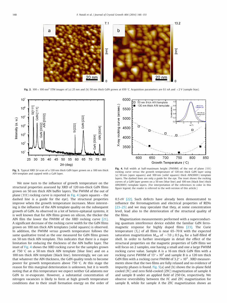
We now turn to the influence of growth temperature on thestructural properties assessed by XRD of 120 nm-thick GdN filmsgrown on 50 nm thick AlN buffer layers. The FWHM of the out ofplane (111) rocking curve is reported in Fig. 4 (open squares – thedashed line is a guide for the eye). The structural propertiesimprove when the growth temperature increases. More interest-ing is the influence of the AlN template quality on the subsequentgrowth of GdN. As observed in a lot of hetero-epitaxial systems, itis well known that for AlN films grown on silicon, the thicker theAlN film the lower the FWHM of the XRD rocking curve [21].A significant decrease of the rocking curve width for the GdN filmsgrown on 100 nm thick AlN templates (solid squares) is observed.In addition, the FWHM versus growth temperature follows thesame qualitative trend as the one measured for GdN films grownon 50 nm thick AlN template. This indicates that there is a majorlimitation for reducing the thickness of the AlN buffer layer. Theinset of Fig. 4 shows the XRD rocking curve for the samples grownat 750 1C on a 50 nm thick AlN template (blue line) and on a100 nm thick AlN template (black line). Interestingly, we can seethat whatever the AlN thickness, the GdN quality tends to becomepoorer for growth temperatures above 750 1C. At this stage thereason for this marginal deterioration is unknown, but it is worthnoting that at this temperature we expect neither Gd adatoms norGdN to re-evaporate. However, a substantial concentration ofnitrogen vacancies is likely to form at high growth temperatureconditions due to their small formation energy on the order of
0.5 eV [22]. Such defects have already been demonstrated toinfluence the ferromagnetism and electrical properties of RENs[23–25] and we may speculate that they, at some concentrationlevel, lead also to the deterioration of the structural quality ofthe films.
Magnetization measurements performed with a superconduct-ing quantum interference device exhibit the familiar GdN ferro-magnetic response for highly doped films [23]. The Curietemperature (TC) of all films is near 65–70 K with the expectedsaturation magnetization Msat of �7.070.5 μB for a half-filled 4fshell. In order to further investigate in detail the effect of thestructural properties on the magnetic properties of GdN films wewill focus on 2 samples, one having a small and one a large FWHMrocking curve value. Sample A is a 16 nm thick GdN film with arocking curve FWHM of 13ʺ�103 and sample B is a 120 nm thickGdN film with a rocking curve FWHM of 3.2ʺ�103 . XRD measure-ments show that the two films are fully relaxed and no evidence ofimpurity phases is found. Fig. 5(a) and (b) shows the in-plane fieldcooled (FC) and zero field-cooled (ZFC) magnetization of sample Aand sample B under an applied field of 250 Oe, respectively. Weobserve reversibility between the FC and ZFC magnetization forsample B, while for sample A the ZFC magnetization shows an
Fig. 2. 100�100 nm2 STM images of (a) 25 nm and (b) 50 nm thick GdN grown at 650 1C. Acquisition parameters are 0.1 nA and þ2 V (sample bias).
Fig. 3. Typical XRD 2θ scan of a 120 nm thick GdN layer grown on a 100 nm thickAlN template and capped with a GaN layer.
Fig. 4. Full width at half-maximum height (FWHM) of the out of plane (111)rocking curve versus the growth temperature of 120 nm thick GdN layer using(a) 50 nm (open squares) and 100 nm (solid squares) thick AlN(0001) templatelayers. The dashed lines are only a guide for the eye. The inset shows the rockingcurves of a GdN layer grown on a 50 nm (blue line) and 100 nm (black line) thickAlN(0001) template layers. (For interpretation of the references to color in thisfigure legend, the reader is referred to the web version of this article.)
F. Natali et al. / Journal of Crystal Growth 404 (2014) 146–151148

abrupt drop below �16–17 K giving a cusp. Clearly, below thistemperature, a field of 250 Oe is not sufficient to fully rotate themagnetic moment along the magnetic field direction, signaling adifference between the magnetic anisotropy of sample A andsample B. This contrast is emphasized by the temperature depen-dence of the coercive field (HC) shown in (Fig. 5(c) and (d)). Weobserve for sample A (Fig. 5(c)) a rapid decrease of HC withincreasing temperature, resulting in the vanishing of hysteresisabove �20 K. The temperature dependence of the coercive fieldcan be understood by considering the crystallographic structure ofthe sample. STM images show a surface composed of small grains,on the order of 9.5 nm, suggesting rather a “ferromagnetic orderednanoparticles” like structure. We believe that the peak at �16–17 K in the ZFC magnetization signals the blocking temperature ofsuperparamagnetism arising from the nanocrystalline structure ofthe films. This is further supported by the inset in Fig. 5(c),showing below 20 K the linear dependence of coercive field onthe square root of the temperature (T1/2) obtained from therelation (equation 1) Hc¼Ho(1�(T/TB))1/2, typical of nanoparticlesamples [26,27]. Ho is the coercive field at 0 K, T is the measure-ment temperature, and TB is the blocking temperature. The datapoints are found to fit reasonably well to equation 1 forTr20 K¼TB. The value of TB agrees well with the temperature ofthe maximum moment of the ZFC curve at 16–17 K. An estimate ofthe magnetic anisotropy K can be obtained using the generalformula for nanoparticles [27]: TB¼KV/25kB where kB is the
Boltzmann constant and V the volume of GdN grains. By consider-ing triangular grains having a base width of 9.5 nm and height of16 nm, we calculate a magnetic anisotropy of �4�105 erg/cm3.A much higher value for the anisotropy of 5�106 erg/cm3 hasbeen reported for nanocrystalline GdN thin films though theauthors suggested that strain might have enhanced the anisotropy[28], while a much smaller value of 2.5�104 erg/cm3 has beencalculated for GdN [29]. Above TB, a rather small coercive fieldvanishing at 40 K is observed that could suggest the presence of asmall population of grains either ferromagnetic or with a higherblocking temperature. A coercive field of only 35 Oe at 5 K ismeasured for sample B, about 7 times smaller than that of sampleA. Once again, we can interpret this result from a crystallographicpoint of view. The larger the grain size, the smaller the coercivefield [1,30]. More interesting is the linear temperature dependenceof the coercive field for this film. This scenario seems to follow themodel proposed by Gaunt for continuous films where the ferro-magnetic domain walls are pinned by a random array of inhomo-geneities such as dislocations or grain boundaries [30]. Accordingto this model, which includes thermal activation, a linear depen-dence of Hc as a function of the temperature implies weak domainwall pinning. The vanishing of hysteresis above 50 K coincides wellwith the separation of the FC and ZFC curves when measuredunder an applied field of 20 Oe (not shown). This result isconsistent with the recent work done by Natali et al. whichsuggests that in GdN a homogeneous ferromagnetic (FM) phase
Fig. 5. In-plane field cooled (FC) and zero field-cooled (ZFC) magnetization of (a) 16 nm thick GdN and (b) 120 nm thick GdN under an applied field of 250 Oe. Temperaturedependence of the coercivity for sample A (c) and sample B (d). The inset in figure (c) shows the linear dependence of coercive field on the square root of the temperature (T1/2).
F. Natali et al. / Journal of Crystal Growth 404 (2014) 146–151 149

exists only below 50 K, leading to the vanishing of hysteresis abovethis temperature [23].
We now examine the effect of the structural quality on theelectrical properties of 120 nm thick GdN films grown at differenttemperatures on a 50 nm AlN buffer layer. Fig. 6(b) shows thevariation of resistivity of the films measured at 300 K in the vander Pauw configuration as a function of the growth temperature.Such low values of resistivity, �10�2 mΩ cm, have been alreadyreported in the literature for unintentionally doped epitaxial GdNlayers and have been associated with a background electroncarrier concentration ranging from 1020 to 1022 cm�3 originatingfrom VN [9,23]. The electron carrier concentration of our GdN films(measured by Hall effect in the same configuration) as a functionof the growth temperature is also shown in Fig. 6(a) (opensquares). The initial decline of the carrier concentration withhigher growth temperatures can thus be explained by thedecreased VN concentration. The VN concentration rises at growthtemperatures above 750 1C may be associated with the escape ofnitrogen from the growth surface due to the small activationenergy of VN. Remarkably, this is a similar trend with the growthtemperature to that of the rocking curve FWHM reported in Fig. 4.This concomitant result, showing a strong correlation between thestructural properties and the carrier concentration, suggests thatVN may be more easily trapped at grain boundaries and disloca-tions. This hypothesis is further supported by the higher resistivityand lower carrier concentration of 120 nm thick GdN films grownon a 100 nm thick AlN buffer layer. As discussed earlier, such thinfilms have a better structural quality than those grown on 50 nmthick AlN buffer layer. Electron carrier concentration reduced by a
factor up to 10 is observed for the sample grown at 750 1C while aresistivity on the order of 5 mΩ cm is measured. Finally, theelectrical characteristic suggests that the resistivity is the resultof a more complex interplay between carrier concentration andmobility involving a strong structural dependence rather than adependence on carrier concentration alone. Further investigationswill clearly be of interest.
4. Conclusion
To summarize, we have investigated the growth by MBE of GdNthin films. It is shown that both the growth temperature of GdNand the thickness of the AlN buffer layer contribute strongly to thestructural quality of the film. Our results also show a strongcorrelation between the structural quality and the electrical andmagnetic properties of the films. In addition, the interpretation weprovide may explain the origin of some of the significant differ-ences revealed by recently published data on the conductive andmagnetic states of REN thin films.
Acknowledgements
We acknowledge funding from the NZ FRST (Grant no.VICX0808), the Marsden Fund (Grant nos. 08-VUW-030 and 13-VUW-1309), and the MacDiarmid Institute for Advanced Materialsand Nanotechnology, funded by the New Zealand Centres ofResearch Excellence Fund. We acknowledge support from GANEX(ANR-11-LABX-0014). GANEX belongs to the public funded “Inves-tissements d'Avenir” program managed by the French AgenceNationale de la Recherche (ANR).
References
[1] F. Natali, B.J. Ruck, N.O.V. Plank, H.J. Trodahl, S. Granville, C. Meyer, W.R.L. Lambrecht, Prog. Mater. Sci. 58 (2013) 1316.
[2] B.J. Ruck, in: F. Nasirpouri, A. Nogaret (Eds.), Nanomagnetism and Spintronics,World Scientific, Singapore, 2009.
[3] K. Senapati, M.G. Blamire, Z.H. Barber, Nat. Mater. 10 (2011) 849.[4] M.G. Blamire, A. Pal, Z.H. Barber, K. Senapati, Proc. SPIE 8461 (2013) 84610J
(Spintronics V).[5] H. Warring, B.J. Ruck, H.J. Trodahl, F. Natali, Appl. Phys. Lett. 102 (2013) 132409.[6] S. Krishnamoorthy, T. Kent, J. Yang, P.S. Park, R.C. Myers, S. Rajan, Nano Lett. 13
(2013) 2570.[7] A. Kandala, A. Richardella, D.W. Rench, D.M. Zhang, T.C. Flanagan, N. Samarth,
arXiv:1212.1225, 2013.[8] W.K. Liu, M.B. Santos, Thin Films: Heteroepitaxial Systems (Eds.), World
Scientific Publishing Company, Singapore, 1999.[9] M.A. Scarpulla, C.S. Gallinat, S. Mack, J.S. Speck, A.C. Gossard, J. Cryst. Growth
311 (2009) 1239.[10] F. Natali, N.O.V. Plank, J. Galipaud, B.J. Ruck, H.J. Trodahl, F. Semond, S. Sorieul,
L. Hirsch, J. Cryst. Growth 312 (2010) 3583.[11] T.F. Kent, J. Yang, L. Yang, M.J. Mills, R.C. Myers, Appl. Phys. Lett. 100 (2012)
152111.[12] R. Vidyasagar, S. Kitayama, H. Yoshitomi, T. Kita, T. Sakurai, H. Ohta, Appl. Phys.
Lett. 100 (2012) 232410.[13] F. Natali, B. Ludbrook, J. Galipaud, N. Plank, S. Granville, A. Preston, B.L. Do,
J. Richter, I. Farrell, R. Reeves, S. Durbin, J. Trodahl, B. Ruck, Phys. Status Solidi C9 (2012) 605.
[14] E.-M. Anton, B.J. Ruck, C. Meyer, F. Natali, H. Warring, F. Wilhelm, A. Rogalev,V.N. Antonov, H.J. Trodahl, Phys. Rev. B 87 (2013) 134414.
[15] J.H. Richter, B.J. Ruck, M. Simpson, F. Natali, N.O.V. Plank, M. Azeem,H.J. Trodahl, A.R.H. Preston, B. Chen, J. McNulty, K.E. Smith, A. Tadich,B. Cowie, A. Svane, M. van Schilfgaarde, W.R.L. Lambrecht, Phys. Rev. B 84(2011) 235120.
[16] Do Le binh, B.J. Ruck, F. Natali, H. Warring, H.J. Trodahl, E.-M. Anton, C. Meyer,L. Ranno, F. Wilhelm, A. Rogalev, Phys. Rev. Lett. 111 (2013) 167206.
[17] F. Semond, Y. Cordier, N. Grandjean, F. Natali, B. Damilano, S. Vézian, J. Massies,Phys. Status Solidi A 188 (2001) 501.
[18] T.L. Goodrich, Z. Cai, K.S. Ziemer, Appl. Surf. Sci. 254 (2008) 3191.[19] M.W. Cho, A. Setiawan, H.J. Ko, S.K. Hong, T. Yao, Semicond. Sci. Technol. 20
(2005) S13.[20] E.A. Paisley, T.C. Shelton, S. Mita, R. Collazo, H.M. Christen, Z. Sitar,
M.D. Biegalski, J.-P. Maria, Appl. Phys. Lett. 88 (2006) 212906.
Fig. 6. (a) Ambient temperature electron carrier concentration as a function of thegrowth temperature for 120 nm thick GdN films grown on AlN template layers witha thickness of 50 nm (open squares) and 100 nm (solid squares). (b) Ambientresistivity as a function of the growth temperature for 120 nm thick GdN filmsgrown on 50 nm thick AlN template layers (solid circles). The dashed lines are aguide for the eye.
F. Natali et al. / Journal of Crystal Growth 404 (2014) 146–151150

[21] Y. Cordier, J.-C. Moreno, N. Baron, E. Frayssinet, J.-M. Chauveau, M. Nemoz,B. Damilano, F. Semond, J. Cryst. Growth 312 (2010) 2683.
[22] A. Punya, T. Cheiwchanchamnangij, A. Thiess, W.R.L. Lambrecht, Mater. Res.Soc. Symp. Proc. (2011), http://dx.doi.org/10.1557/opl.2011.383.
[23] F. Natali, B.J. Ruck, H.J. Trodahl, S. Do Le Binh, B. Vézian, Y. Damilano, F. Cordier,Semond, C. Meyer, Phys. Rev. B 87 (2013) 035202.
[24] N.O.V. Plank, F. Natali, J. Galipaud, J. Richter, M. Simpson, H.J. Trodahl, B.J. Ruck,Appl. Phys. Lett. 98 (2011) 112503.
[25] K. Senapati, T. Fix, M.E. Vickers, M.G. Blamire, Z.H. Barber, Phys. Rev. B 83(2011) 014403.
[26] E.F. Kneller, F.E. Luborsky, J. Appl. Phys. 34 (1963) 656.[27] M. Knobel, W.C. Nunes, L.M. Socolovsky, E. De Biasi, J.M. Vargas, J.C. Denardin.,
J. Nanosci. Nanotechnol. 8 (2008) 2836.[28] K. Khazen, H.J. von Bardeleben, J.L. Cantin, A. Bittar, S. Granville, H.J. Trodahl,
B.J. Ruck, Phys. Rev. B 74 (2006) 245330.[29] S. Abdelouahed, M. Alouani, Phys. Rev. B 79 (2009) 054406;
M. Alouani, Private Communication (2013).[30] P. Gaunt, Philos. Mag. B 48 (1983) 261;
X. Chen, P. Gaunt, J. Appl. Phys. 65 (1989) 3980.
F. Natali et al. / Journal of Crystal Growth 404 (2014) 146–151 151