Jlm~t - Yakın Doğu Üniversitesi I neu.edu.tr
117
NEAR EAST UNIVERSITY Faculty of Engineering Department of Electrical and Electronic Engineering FRUIT PACKING OTOMATION SYSTEM (PLC) GRADUATION PROJECT EE-400 Student: AliKsan Taşdemir (9511'12) Supervisor: Özgür C. Özerdem ~~.,~~~~Jlm~t NEU LefKoşa - 2001
Transcript of Jlm~t - Yakın Doğu Üniversitesi I neu.edu.tr

NEAR EAST UNIVERSITY
Faculty of Engineering
Department of Electrical and ElectronicEngineering
FRUIT PACKING OTOMATION SYSTEM(PLC)
GRADUATION PROJECTEE-400
Student: Aliksan Taşdemir (9511'12)
Supervisor: Özgür C. Özerdem
~~.,~~~~Jlm~tNEU
Lefkoşa - 2001
-'r,,?-- ~ \
I
,efJı1~(t:. -;:;,
1
11
ACKNOWLEDGEMENT . LIST OF ABREVATIONS . ABSTRACT... . . . . . . . . . . . . . . . . . . . . . . . . . . . . . . . . . . . . . . . . . . . . . . . . . . . . . . . . . . . . . . . . . . . . . . . . . . . . . . . . 111
1. Introduction. . . . . . . . . . . . . . . . . . . . . . . . . . . . . . . . . . . . . . . . . . . . . . . . . . . . . . . . . . . . . . . . . . . . . . . . . . . . . . . . 11.1 Basics of programmable logic controllers 21.2 Logic 31.3 The laws of boolean algebra.......................................................... 61.4 Ladder diagram. . . . . . . . . . . . . . . . . . . . . . . . . . . . . . . . . . . . . . . . . . . . . . . . . . . . . . . . . . . . . . . . . . . . . . . . . 7
2. Design, structure and operation 102 .1 PLC architecture. . . . . . . . . . . . . . . . . . . . . . . . . . . . . . . . . . . . . . . . . . . . . . . . . . . . . . . . . . . . . . . . . . . . . . . 1 O2.2 CPU 132.3 Memory 142.4 Bus 162.5 Input/output interfaces 16
2.5.1 D.C. voltage digital input circuit. 172.5.2 AC. voltage digital input circuit 182.5.3 Pulse counter interface 182.5.4 Analogue to digital converter (ADC) interface 202.5.5 Transistor output circuit 212.5.6 Tnac output interface 222.5.7 Digital to analogue converter (DAC) interface 22
2.6 Input/ output assignment. 242.7 Keyboard and display 252.8 Program execution 262.9 Multitasking and multiprocessing 282.10 Development systems 28
3. Input devices 303 .1 Digital devices... . . . . . . . . . . . . . . . . . . . . . . . . . . . . . . . . . . . . . . . . . . . . . . . . . . . . . . . . . . . . . . . . . . . . . . . 30
3 .1.1 Pressure and temperature switches 303 .1.2 Proximity switches 303.1.3 Photoelectric switches 323.1.4 Optical switches 35
3.2 Analogue devices 373 .2 .1 Linear potentiometer. . . . . . . . . . . . . . . . . . . . . . . . . . . . . . . . . . . . . . . . . . . . . . . . . . . . . . . . . . . . 3 73.2.2 Linear variable differantial transformer (LVDT) 383.2.3 Tachogenerator. 393 .2 .4 Temperature sensor.. 3 93.2.5 Strain gauge 42
3 .3 Basic interfacing techniques 434. Programming methods 47
4.1 Graphical languages 474 .1.1 Ladder diagram (LD) 474.1.2 Function block diagram (FBD) 48
4.2 Sequential function chart 494 .3 Translating between languages 53
'5. Ladder programming examples 555.1 Combinationallogic 555 .2 Latching 605 .3 Generating a pulse signal 615.4 Timers 625.5 Counters 645 .6 Shift register 665.7 Conditional jumps and subroutines 675.8 Arithmetic functions 67
6.Tutorial examples 696. !Deriving a ladder diagram from a truth table 696.2An off-delay timer circuit 726.3Controlling output using timers 726.4Cyclic timer. 76
7.Application examples 787. lExample 1: control of a pneumatic piston 787.2Example 2: sequencing of three pneumatic piston 807.3Example 3 counting and packaging 817.4Example 4 : component detection and sorting 857.SExample 5: pick and place unit 877.6Example 6 checking for a missing bottle cap 877.7Example 7 : PD temperature control 89
TABLE OF SYMBOL 96MY PROJECT DRAWING AND INTRODUCTION 97CONCLUSION .103REFERENCES 104APPENDIX 105

ACKNOWLEDGEMENTS
First of all, I want to thank to my teacher's the supervisor Mr.Özgür C.
ÖZERDEM , Mr. Kaan UYAR, and Mr.Mherdad KHALEDİ for supporting me
durring my education.Also thanks to Prof.Haldun GüRMEN , Prof. Dr. Fakhreddin MAMEDOV ,
Prof. Dr. Şenol BEKTAŞ and Prof. Dr. Khalil İSMAiLOV
Then I wish to thank to my friends Altınay ORMAN , Bora E. TUGLU, Orhan
ŞADİ Fatoş GÜVEN and Bülent GÜVEN for their help. And finally I want to thank
everybody who helped and suppurted me from my first day at the university till my
graduation.
ii
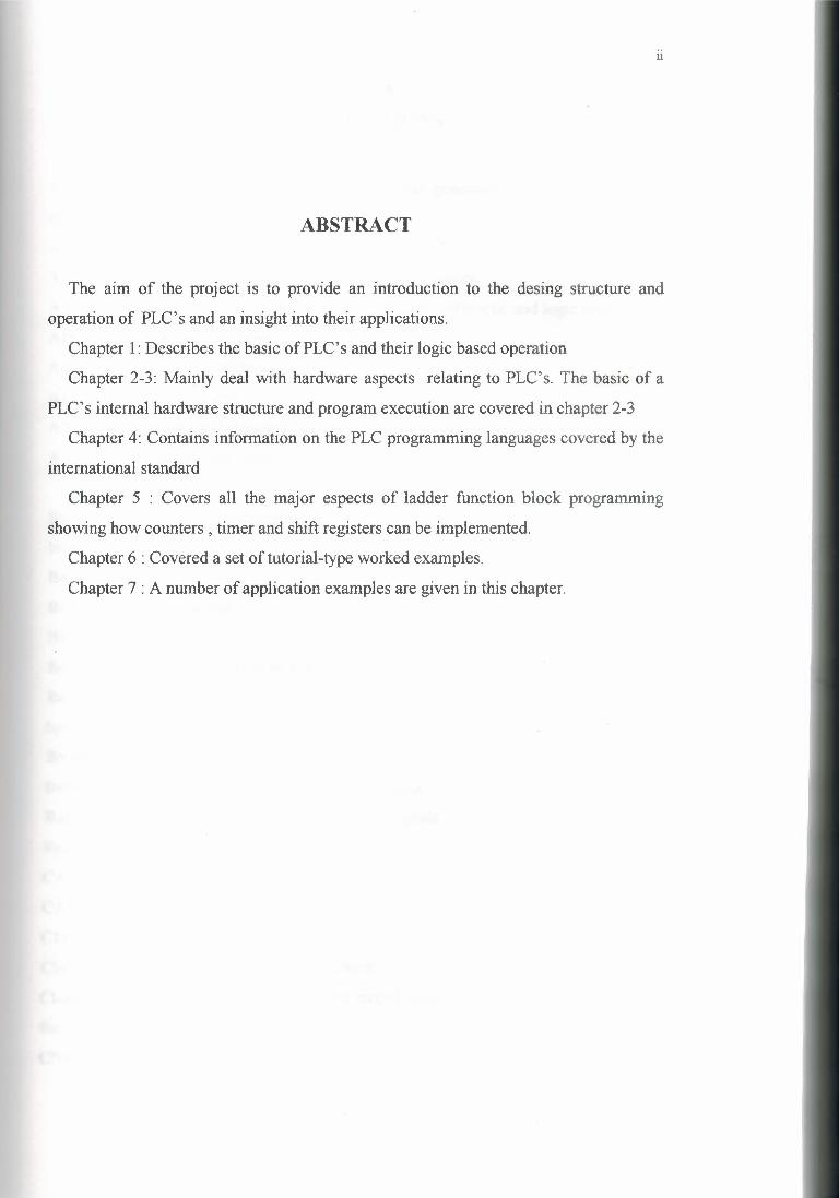
ABSTRACT
The aim of the project is to provide an introduction to the desing structure and
operation of PLC's and an insight into their applications.
Chapter 1: Describes the basic ofPLC's and their logic based operation
Chapter 2-3: Mainly deal with hardware aspects relating to PLC' s. The basic of a
PLC' s internal hardware structure and program execution are covered in chapter 2-3
Chapter 4: Contains information on the PLC programming languages covered by the
international standard
Chapter 5 : Covers all the major espects of ladder function block programming
showing how counters , timer and shift registers can be implemented.
Chapter 6: Covered a set of tutorial-type worked examples.
Chapter 7 : A number of application examples are given in this chapter.
111
ABBREVIATIONS
Absolute encoder A shaft or linear encoder that generates a unique number for
resolvable position
A.C. or a.c, Alternating currentAccess time The time taken for data to be read from memoryAcumulator A CPU register used to hold the results of arithmetic and logic operations
ADC Anologue to digital converter.Address The numerical assingment of a particular memory location
ALU Arithmetic logic unit.
ANSI American national standard institute
ASCII American standard code for information interchange
Bandwidth Iformation carrying capacity of a communication channel expressed in
bits/s.Baud A unit of transmission.
BCD Binary code decimal
Bit Binary digit
Boolean data Data represented as a single bit.
Boot To load an operating system
bps Bts per second
BS british standartBuff er A bolck of memory used for temporary storage
Bus A set of conductors used for communicating signals
Byte A group of eight bits
CAD Computer aided design
CAM Computer aided manufacture
CiM Computer integrated manufacture
Clock Aperiodic signal used for synchronizationClosed-loop control A system in which the output signal is measured and fed back to
the input point.
CNC Computer numerical control
ıv
Contact bounce The problem relating to mechanical switches which produce a noisy
signal when swithedCompiler A program to translate a high-level language into machine code
Counter A function block that gives an output when a set number of pulses have been
applied to the input
CPU Central processing unitCSMA/CD Carrier sense multiple access with collusion detection
Current sinking The action of receiving current
DAC Digital to analog convector
EEPROM Electrically erasble programmableread only memory
EPROM Electrically programmableread only memory
FET Field effect transistorFlag A single bit variable used the indicate that some conditions has occurred
Full dublex A full dublex data link allows the transmission data simultaneously
İn bth directionGateaway A device thas connects and allows messages to be communicated between to
or more dıfferet network systemGray code A binary code in which consecutive codes differ in only a single bit position
Hexadecimal Base 16 number system
Hz Hertz .the unit of frequency equal to one cycle per second
IC Integrated circuit
IEC İnternational electrotechnical commisions
IEE Institute of electrical enngineers
IEEE Institute of electrical and eletronic eng.Ladder diagram A programming language in which a circuit, consisting of contacts ,
coils and other elements, such as functions blocks, and bounded between left and right
vertical lines.
LSB Least significant bit
Machine code Binary number that represent CPU instruction
MSB Most significant bit
MTBF Mean time between failure
N/C Normaly closed
N/0 Normaly open
Off-delay timer A function block that holds its output high for a specified duration
when its input changes from high to lowOn-delay timer A function block that delays setting its output high when its input
changes from low to highProgram counter A CPU register containing the address of next instruction to be
executedProgramming language IEC - defined programming languages are function block
diagram (FBD)
RAM Random access memory
ROM Read only memoryRun The run mode executes the user program stored in memory
Scan PLC program execution loop to continously read input values and set outputs
according to the program requirement
State The condition of a Boolean variableTachogenerator A permanent magnet d:c: motor operated as a voltage generator:
TTL Transistor-transistor logic.Two's complement A system for representing negative numbers in binary notation
V
1
CHAPTER 1
Information about PLC
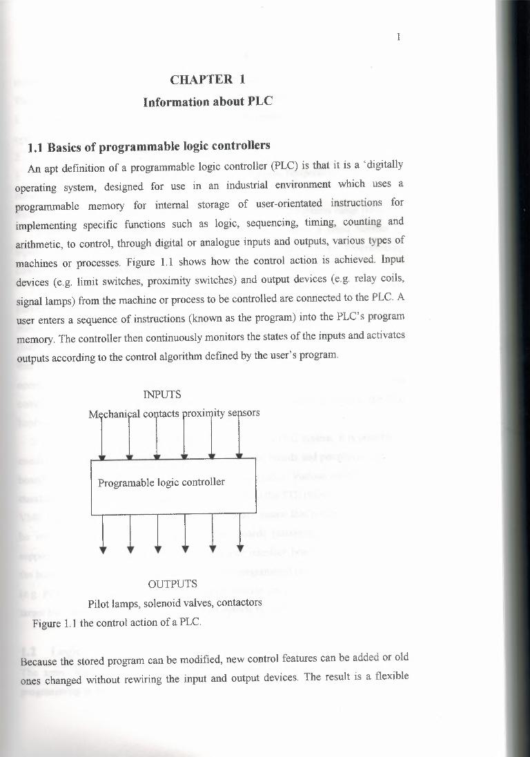
1.1 Basics of programmable logic controllers An apt definition of a programmable logic controller (PLC) is that it is a 'digitally
operating system, designed for use in an industrial environment which uses a
programmable memory for internal storage of user-orientated instructions for
implementing specific functions such as logic, sequencing, timing, counting and
arithmetic, to control, through digital or analogue inputs and outputs, various types of
machines or processes. Figure 1.1 shows how the control action is achieved. Input
devices (e.g. limit switches, proximity switches) and output devices (e.g. relay coils,
signal lamps) from the machine or process to be controlled are connected to the PLC. A
user enters a sequence of instructions (known as the program) into the PLC's program
memory. The controller then continuously monitors the states of the inputs and activates
outputs according to the control algorithm defined by the user's program.
INPUTS
Mechanical contacts nroxı ors
Programable logic controller
OUTPUTS
Pilot lamps, solenoid valves, contactors
Figure 1.1 the control action of a PLC.
Because the stored program can be modified, new control features can be added or old
ones changed without rewiring the input and output devices. The result is a flexible
2
system which can be used for control tasks that can vary in nature and complexity.
The main differences between a PLC and, say, a microcomputer are that:
1. Programming is predominantly concerned with control logic and function block
operations.
2. Interfacing circuits are integral to the controller.
3. PLCs are rugged, being packaged to withstand vibration, temperature, humidity and./
noıse.Some typical programmable controllers are shown in Fig. 1.2.2 Systems range from:
I.Stand-alone single unit PLC systems. These systems have a fixed number of
input/output (I/0) points and are suited for small I/O automation tasks. Programming
consoles are usually hand-held units which attach directly to thePLC.
2.Modular PLC systems. These systems are composed of self-contained hardware
building blocks (modules), which plug directly into a proprietary bus back plane. A
minimum configuration would utilize a CPU unit, a power supply unit and input/output
(both digital and analogue) modules. The modular approach to PLC hardware means
that the number and type of I/O points can be expanded. Special function modules for
operations such as networking and computer linking are often provided. A host
computer is usually used to develop program code, which is then targeted to the PLC
hardware.3.Computer bus based systems. Although not strictly a PLC system, it is possible to
construct a custom computer controller using processor boards and peripheral interface
boards which plug into a common bus back plane (rack). Various international bus
standards have been developed for this purpose such as the STE (Euro card) bus and the
VME bus. The modular approach to target hardware means that processing power can
be increased by adding additional processor boards (assuming multiprocessing is
supported by a bus scheduler) and special purpose interface boards can be designed to
the bus standard. Bus based systems are usually programmed using high level language
(e.g. PASCAL and C) cross compilers which execute on a host computer and which
target hardware on the bus. Such systems fall outside the scope of this book.
1.2 Logic The term 'logic' features in the name 'programmable logic controllers' because
programming is based on the logic demands of input devices. Programs implemented
3
are predominantly logical rather than discrete versions of continuous algorithms. This
section provides an introduction to logic.
The field of logic is concerned with systems that work on a straightforward two-state
basis. A common electric light switch can be either on or off and these alternate
possibilities can be labeled as true and false or as 1 and O (binary form) respectively. A
Boolean variable (i.e. a logical variable) such as A can be-used to represent any switch
like element, which can have one of two states. For example, it is possible to define
thatA=l when the switch on andA=O when the switch is off
Any condition in which there are two possibilities can be defined using a Boolean
variable. For example, a work piece can be in or out of position. This may be
represented as a simple binary statement B=l (work piece is in position) or B=O (work
piece is not in position). Another example is a lamp, which can be either on or off
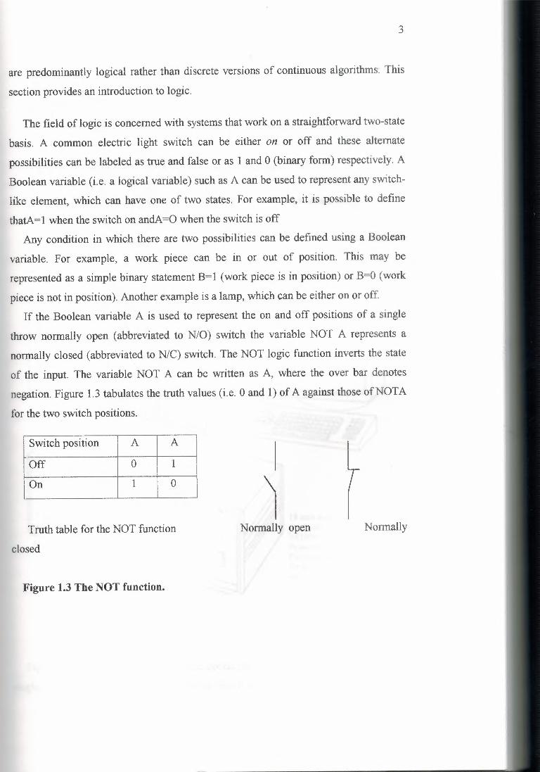
If the Boolean variable A is used to represent the on and off positions of a single
throw normally open (abbreviated to N/0) switch the variable NOT A represents a
normally closed (abbreviated to N/C) switch. The NOT logic function inverts the state
of the input. The variable NOT A can be written as A, where the over bar denotes
negation. Figure 1.3 tabulates the truth values (i.e. O and 1) of A against those ofNOTA
for the two switch positions.
Switch position A A
Off o 1
On 1 o
Truth table for the NOT function
closed
Normally open Normally
Figure 1.3 The NOT function.

4
Small relay replacement.£130-i800 8-100/1/0Simple programming
Medium sized unit.£400-.£2000 aesoe rıoAdvanced programming £unctions
Large system>.£1000>60 uo Colour operator terminalAdvanced programmingspedalized moduln
19 inch rack industrialcomputer>£1000Powerful 1/0Full computer powerfor proerainminc andoperation
The AND logic function describes the operation of two normally open single-pole,
single-throw switches connected in series as shown in Fig. 1.4. Current flows only when
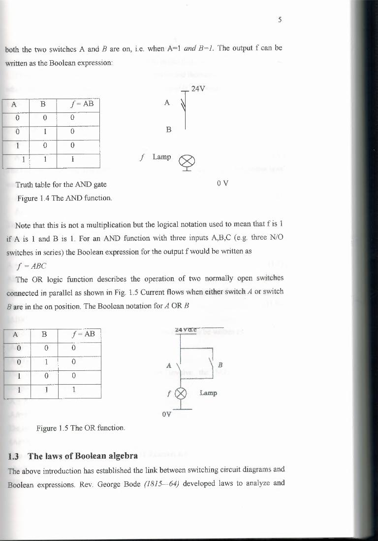
5
both the two switches A and Bare on, i.e. when A=l and B=I. The output f can be
written as the Boolean expression:
I A B f=AB
I o o o
I o 1 o
I 1 o o
I 1 1 1
A
B
f Lamp ~
Truth table for the AND gate
Figure 1.4 The AND function.
ov
Note that this is not a multiplication but the logical notation used to mean that f is 1
if A is 1 and B is 1. For an AND function with three inputs A,B,C (e.g. three N/0
switches in series) the Boolean expression for the output f would be written as
f =ABCThe OR logic function describes the operation of two normally open switches
connected in parallel as shown in Fig. 1.5 Current flows when either switch A or switch
B are in the on position. The Boolean notation for A OR B
A B f=ABI o o oII o 1 o
I 1 o o
I 1 1 1 I Lamp
ovFigure 1.5 The OR function.
1.3 The laws of Boolean algebra The above introduction has established the link between switching circuit diagrams and
Boolean expressions. Rev. George Bode (1815-64) developed laws to analyze and
6
construct logical statements. Boolean algebra deals with two-valued variables and is
useful when analyzing switching circuits such as ladder diagrams.
The laws of Boo lean algebra consist of postulates and theorems. The four postulates,
whicn deal with the combination of one Boolean variable and with, the constants O and
1 are
A+O=A (1.1)
A+l=l (1.2)
AO=O (1.3)
Al=A (1.4)
The two postulates that deal with one variable with itself are called the idem potent laws
and are
A+A=A
AA=A
(1.5)
(1.6)
The commutative laws emphasize the fact that the position of the variables in an
expression is not important. The commutive laws are
A+B=B+A
AB=BA
(1.7)
(1.8)
The associative laws deal with the use of brackets at can be expressed as
(A+B) + C =A+ (B+C)
(AB)C = A(BC)
(1.9)
(1. 10)
The distributive laws show how factors are combined and can be written as
(AB)+ (AC) =A (B+C)
(A+B)(A+C) =A+ (BC)
(1.11)
(1.12)
The complementarity' s and involution laws involve the NOT function. The
complementarity' s laws are
A+A=l
Ak=O
(1.13)
(1.14)
The involution law is
(A)=A (1.15)
T.wo o.ther_postulates that involve the NOT function are called De Morgan's theorems
which are
(AB)=A+B (1.16)
7
(A +B)=A B (1.17)
The function A AND B all negated (i.e. (AHJ1s called the NAND function. NAND is an
abbreviation for NOT AND. Similarly, the function A ORB all negated (i.e. (A + B)) is
called the NOR function. NOR is an abbreviation for NOT OR
There are two branches of logic called combinational logic and sequential logic. A
combinational logic system is one in which the output is a direct and unique
consequence of the input conditions. A sequential logic system is one that depends on
the sequence in which the inputs occur. This introduction has dealt with combinational
logic. Sequential logic devices (e.g. flip-flops, shift registers) are discussed in Chapter
5.
1.4 Ladder diagrams PLCs were developed to offer a flexible (e.g. programmable) alternative to
conventional electrical circuit relay-based control systems built using discrete devices.
The terminology and other concepts used to describe the operation of a PLC are based
on conventional relay control terminology. The relationship is such that inputs are
referred to as contacts, outputs are referred to as coils and memory elements (bits) are
referred to as auxiliary relays.
The International Electro technical Commission (IEC) advocates five programming
methods for PLCs, which are fully discussed in Chapter 5. Of these five, the
predominant programming method used by all mainstream PLC systems is the ladder
diagram method. This is a graphical programming technique, which has been evolved
from conventional electrical circuit relay logic control methods. PLC systems provide a
design environment (either in the form of software tools running on a host computer
terminal or a hand-held LCD graphic programming console), which allow ladder
diagrams to be developed and diagnosed.
In its simplest form, a ladder diagram is a network of contacts and coils bounded on
the left and (optionally) on the right by vertical lines called power rails. The key
features of a ladder diagram are:
1. Contacts represent the states of Boolean variables. For example, a contact called
'start_fan' might represent the ON and OFF state of a switch which is used to initiate a
ladder rung which operates a fan. The ladder symbols for normally open and normally
closed contacts are and respectively.
8
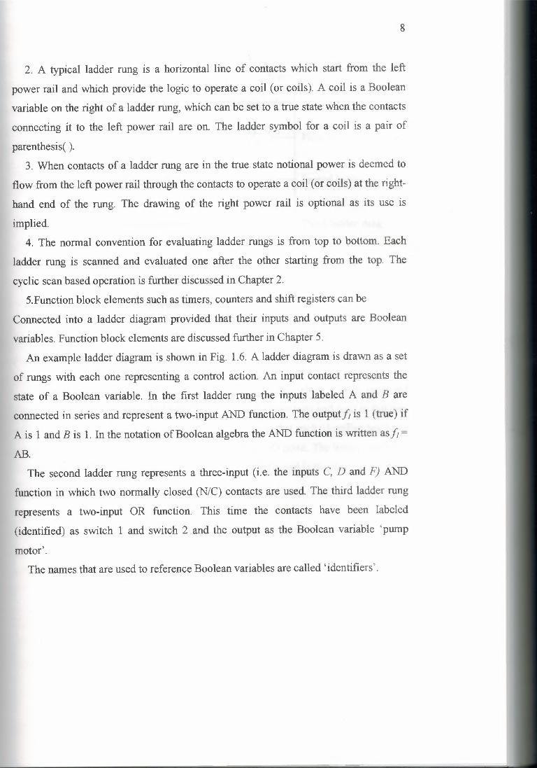
2. A typical ladder rung is a horizontal line of contacts which start from the left
power rail and which provide the logic to operate a coil (or coils). A coil is a Boolean
variable on the right of a ladder rung, which can be set to a true state when the contacts
connecting it to the left power rail are on. The ladder symbol for a coil is a pair of
parenthesis( ).
3. When contacts of a ladder rung are in the true state notional power is deemed to
flow from the left power rail through the contacts to operate a coil (or coils) at the right
hand end of the rung. The drawing of the right power rail is optional as its use is
implied.4. The normal convention for evaluating ladder rungs is from top to bottom. Each
ladder rung is scanned and evaluated one after the other starting from the top. The
cyclic scan based operation is further discussed in Chapter 2.
5.Function block elements such as timers, counters and shift registers can be
Connected into a ladder diagram provided that their inputs and outputs are Boolean
variables. Function block elements are discussed further in Chapter 5.
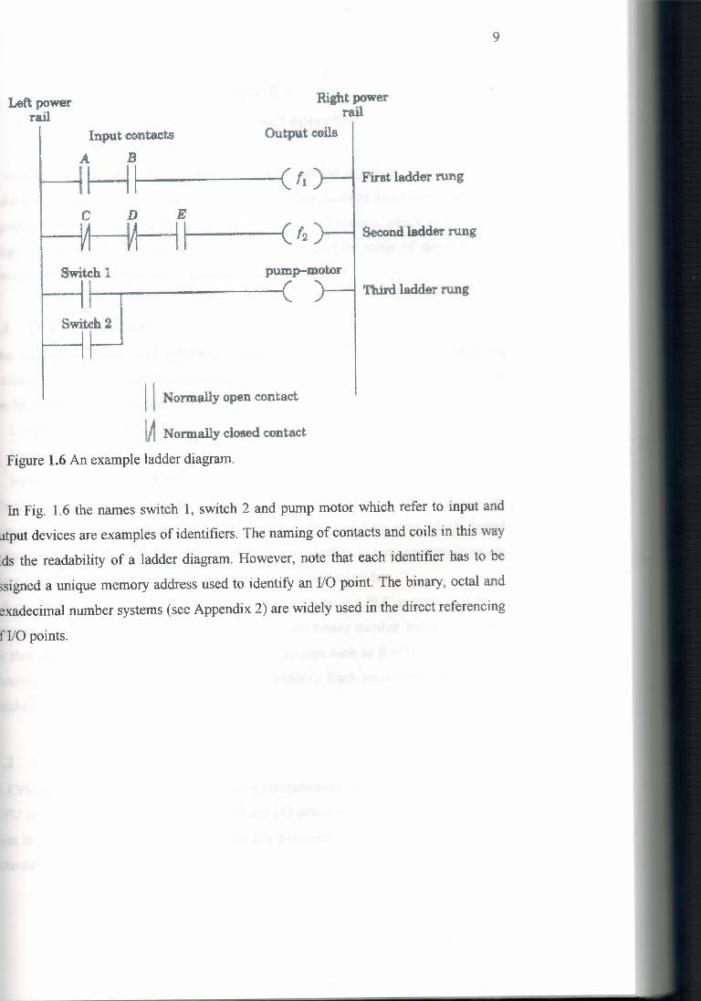
An example ladder diagram is shown in Fig. 1.6. A ladder diagram is drawn as a set
of rungs with each one representing a control action. An input contact represents the
state of a Boolean variable. In the first ladder rung the inputs labeled A and B are
connected in series and represent a two-input AND function. The output/I is 1 (true) if
A is 1 and B is 1. In the notation ofBoolean algebra the AND function is written as/I =AB.
The second ladder rung represents a three-input (i.e. the inputs C, D and F) AND
function in which two normally closed (N/C) contacts are used. The third ladder rung
represents a two-input OR function. This time the contacts have been labeled
(identified) as switch 1 and switch 2 and the output as the Boolean variable 'pump
motor'.The names that are used to reference Boolean variables are called 'identifiers'.
9
Left powerrail
Right powerrail
Input contacts
A B ı ı H I ( ı, )----j First ladder rung
Output coils
E I l/1 ,,I - I ı C /2
C D Second ladder rung
Switch 1 pump-motorThird ladder rung
Switch 2
11 Normally open contact
~ Normally dosed contact
Figure 1.6 An example ladder diagram.
In Fig. 1.6 the names switch 1, switch 2 and pump motor which refer to input and
utput devices are examples of identifiers. The naming of contacts and coils in this way
ids the readability of a ladder diagram. However, note that each identifier has to be
ssigned a unique memory address used to identify an I/O point. The binary, octal and
exadecimal number systems (see Appendix 2) are widely used in the direct referencing
f I/O points.
10
CHAPTER2
Design, structure and operation
A modern PLC is a microprocessor-based control system designed to operate in an
industrial environment. PLCs are programmed to sense, activate and control industrial
equipment and therefore incorporate a large number of I/O points, which allow a wide
range of electrical signals to be interfaced. In this chapter some of the important
concepts behind the design ofPLC hardware are presented.
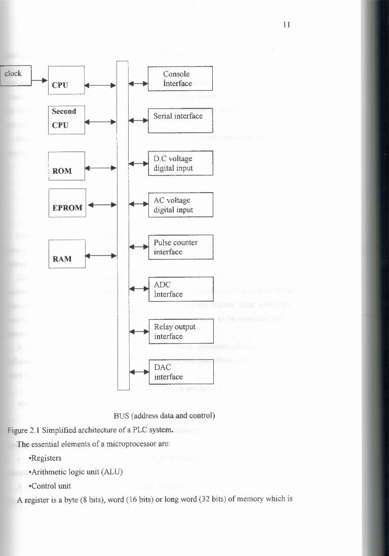
2.1 PLC architecture The internal hardware and software configuration of a PLC is referred to as its
architecture. Being a microprocessor-based system the design of a PLC is based around
the following building blocks:
• Central processing unit (CPU)
• Memory
• Input/output interface devicesThese elements are semiconductor integrated circuits (ICs). They are interconnected by
means of a bus as shown in Fig. 2.1. A bus is a group of lines over which digital
information (e.g. 8 bits of data) can be transferred in parallel. In most systems there are
three distinct buses: the data bus, the address bus and the control bus.
A program written by the user determines the operation of a PLC system. High-level
programs such as ladder diagrams are converted into binary number Instruction codes
so that they can be stored using digital memory devices such as RAM (random access
memory) or programmable ROM (read only memory). Each successive instruction is
fetched, decoded and executed by the CPU.
2.2 CPU A CPU generally takes the form of a single microprocessor device. The function of the
CPU is to control the operation of memory and I/O devices in the system and to process
data in accordance with the program. To do this it requires a clock signal to sequence its
internal operations.
cictll I~~
Second
CPU
[;;IEPROMI
11
~ı.. Console~ - İnterface...• •..
t--- ~ - Serial interface...• •..
t--- ~ ~ D.C voltage~ •.. digital input
••• ••~ ~ AC voltage~ •..
digital input
ı- ~ - Pulse counter...• •...interface
~ ~ ADC...• •..İnterface
~ - Relay output...• r interface
~ ~ DAC...• •..interface
.._
BUS (address data and control)
Figure 2.1 Simplified architecture of a PLC system.
The essential elements of a microprocessor are:
-Registers
-Arithmetic logic unit (ALU)
-Control unit
A register is a byte (8 bits), word (16 bits) or long word (32 bits) ofmemory which is
12
part of the microprocessor as opposed to general purpose memoıy. A register is used for
temporaıy storage of data and addresses within the CPU. The ALU performs arithmetic
and logical operations such as addition and subtraction on data stored in registers. The
control unit is basically a set of counters and logic gates, which is driven by the clock.
Its function is to control the units within the microprocessor to ensure that operations
are carried out in the correct order.
Some CPU registers are accessible to the programmer while others are not. Some
registers common to most microprocessor devices are:
• Data registers
• Address registers
• A program counter
• A flag register
• A stack pointer
Data registers hold data, which is to be operated on by the ALU. A bit pattern moved
into a data register can be added, subtracted, compared, etc., with another bit pattern
stored in a separate data register.
Each memoıy location in RAM and ROM for storing data is given an unique
address. The programmer to specify source and destination addresses of data items to be
manipulated can use CPU address registers. The program counter (also called the
instruction pointer) holds the address of the next instruction to be executed and is
automatically incremented by the CPU.
A flag register is a collection of single-bit status indicators (flags) that holds
information about the result of the most recent instruction that affects them. Commonly
used flags are:
• Carıy bit Set to 1 if a binaıy addition operation produces a carıy or a subtraction
operation produces a borrow.
• Zero bit Set to 1 whenever the result of an operation is zero.
• Negative bit In signed binaıy arithmetic it indicates the sign (positive or nega
tive) of the result.
• Overflow Set to 1 when the result of an arithmetic operation cannot be repre
sented in the specified register size.
A stack is a variable length data structure in which the last data item inserted is the
first to be removed. A stack pointer register contains the address of the top element of
13
the stack. The CPU uses the stack to store subroutine return addresses for example.
The execution time of each instruction code takes a specific number of clock cycles.
The clock cycle time is the reciprocal of the clock frequency. For example, a 10 MHz
clock has a clock cycle of O .1 µs.
2.3 Memory Memory devices store groups of binary digits (usually bytes) at individual locations
identified by their own unique addresses. Memory devices are ICs having an address
input (commonly 16 bits wide) and an in/out data port (commonly 8 bits wide). There
are two main types of memory, namely RAM (random access memory) and ROM (read
only memory). The number of binary digits it can hold determines the storage capacity
of a memory device. A IK-byte memory device is capable of storing 1024(i.e. 210)
bytes.A large proportion of the total addressable memory space is devoted to RAM, which
is capable of having data written to it and read from it by the CPU. RAM is used for
program and data storage. A backup battery supply is needed to retain the memory
contents of RAM, as stored data is lost when the power is removed.There are two main types of RAM, namely SRAM (an abbreviation for static RAM)
and DRAM (an abbreviation for dynamic RAM). Static RAM holds data in flip-flop
type cells, which stay in one state until rewritten. SRAM has a fast data access time of
typically 10-20 ns. Dynamic RAM requires special circuitry to provide a periodic
refresh signal in order to maintain the stored data. This is because DRAM technology
stores data in capacitor type cells, which must be periodically refreshed as capacitors
discharge as time increases. DRAM is cheaper to manufacture but because a refresh
signal is used access time is slower than that of SRAM, typically 50-60 ns.
The PLC operating system (i.e. the program that allows the user to develop and run
applications software) is stored in a type of memory referred to as ROM. Once
programmed, this type of memory can only be read from and not written to but does not
lose its contents when the power is removed.Common types of read only memory that are user programmable are EPROM
(erasable programmable read only memory) and EEPROM (electrically erasable
programmable read only memory). EPROM's are programmed using a dedicated
programmer and erased by exposing a transparent quartz window found in the top of
14
.ach device to ultraviolet light. The erasing process clears all memory locations and
akes between 1 O and 20 minutes. EEPROM is erased using electrical pulses rather than
ıltraviolet light. Most PLC systems provide facilities that allow application software to
ıe stored in either EPROM or EEPROM.
t\. memory map is used to indicate how address locations are allocated to ROM, RAM
ınd input/output devices. IfI/0 devices are placed in the memory address space they are
mid to be memory mapped and access to I/O points is via load and store memory
instructions. This has the advantage that common sets of instructions are used for
memory and I/O operations. A memory map of a typical PLC system is shown in Fig.
2.2.
2.4 Bus A bus can be considered as a set of lines over which digital information (e.g. Iô-bit
address or 8-bit data) can be transferred in parallel. In most systems there are three
distinct buses:
• Data bus
• Address bus
• Control busThe data bus is a bi-directional path on which data can flow between the micro-
processor, memory and I/0. An 8-bit microprocessor has a data bus, which is 8 lines
vide.A 16-bit microprocessor has a data bus, which is 16 lines wide.The address bus is a unidirectional set of lines, which carry binary number addresses.
The CPU generates addresses during the execution of a program to specify the source
and destination points of the various data items to be moved along the data bus. An
address identifies a particular memory location or I/O point.
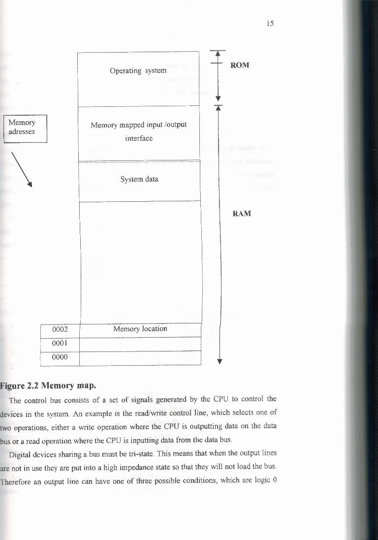
Memoryadresses
\
15
Operating system
J Memory mapped input /output
interface
......................................................................................................................
System data
0002 Memory location
0001
0000
ROM
RAM
Figure 2.2 Memory map. The control bus consists of a set of signals generated by the CPU to control the
devices in the system. An example is the read/write control line, which selects one of
two operations, either a write operation where the CPU is outputting data on the data
bus or a read operation where the CPU is inputting data from the data bus.
Digital devices sharing a bus must be tri-state. This means that when the output lines
are not in use they are put into a high impedance state so that they will not load the bus.
Therefore an output line can have one of three possible conditions, which are logic O

low), logic 1 (high) and output disconnected. Tri-state devices incorporate a chip select
also called chip enable) input, which is used to isolate its data output lines from the
ms. When the chip select line is not active the data output lines are placed in to the high
ımpedance or tri-state. The control bus co-ordinates the connection of the various
:levices to the data bus.
2.5 Input/output interfaces ~croprocessors are supported with special purpose peripheral VO ICs to enable them
to interface with external devices such as keypad displays, sensors and load actuators.
Examples of special purpose VO ICs include keyboard controllers, programmable
parallel interface devices, programmable serial interface devices and counter/timer
devices.As far as the user is concerned, it is the front end circuits to which sensors and
actuators are connected that is important. Input points can include the following types of
interface:• D.C. voltage digital input circuit
• AC. voltage digital input circuit
• Pulse counter circuit
• ADC interfaceOutput points can include the following types of interface:
• Relay output circuit
• Transistor output circuit
• Triac output circuit
• DAC interface
2.5.1 D.C. Voltage digital input circuit Figure 2.3 illustrates typical 24 V D.C. input circuits for connecting current sinking and
sourcing input devices. With the sink input interface the input device when turned on
connects the circuit to the O V line of the D.C. supply. Current then flows through the
status LED (light-emitting diode) used to indicate the current logic state of the input
point and the opto-isolator.An opto-isolator combines an LED and photoelectric transistor. When current is
passed through the LED it emits light, causing the photoelectric transistor to turn on.
16
17
·ovideda separate supply is used for the LED and photoelectric transistor circuits a
.ry large degree of isolation is maintained between the two components.
24Vd.c.-.-24V d.e,
~ 'l'ermiruil connectionon PLC....._Status LED
....••••..
.. -r··--------: : 'To internali ~ C CPU cirouit
Inputdevice
: *1 · -- · ,.r:- 'lb internal: f ~r--.,_j_ CPU circuit1
Opto-isolator
~ St.atl16LED
-----· .... -·
__________..Opto-isolator
Input r-<' Tonn.inalconnectiondevice~ onPLC
ov ov
(a) (b)
'igure 2.3 D.C. voltage digital input circuits: (a) sink input circuit and (b) source
ııput circuit.With the current sourcing interface the input device, when turned on, connects the
ircuit to the positive polarity of the supply (i.e. 24 V). Current flows from the supply
hrough the status LED and opto-isolator circuit.
t.5.2 A.C. Voltage digital input circuit'igure 2.4 illustrates an a.c. voltage digital input circuit. A full-wave diode bridge
.ircuit is used to convert the a.c. input signal into a rectified D.C. signal. The status
..ED and opto-isolator are turned on by the rectified D.C. signal.
Input device
__.,,- (• f
A.C. ~voltage
souree
;- -ı· - · - -~ To intern.al : ~ ıtL_ CPU circuit l - -···--*
Opto-isolator
~ure 2.4 A.C. voltage digital input circuit.
i.3 Pulse counter interface ecial purposes ICs are available which integrate a high-speed digital pulse counter
cuit and buffer memory. Input modules based around these ICs can be used to read
lse streams from an input device such as a shaft encoder. The advantage of using such
ıdules is that high-speed pulse counting is not slowed down by the cyclic scan
eration of a PLC because the counter circuit operates independently. Provided the
.mory buffer is accessible to the ladder program it can be read at the point in time
ten the pulse count value is required. It is also possible to use a technique whereby the
µı-speed counter circuit interrupts the CPU when the count value reaches some pre
fıned limit.
5.4 Analogue to digital converter (ADC) interface t analogue input circuit will incorporate an analogue to digital converter (ADC)
vice, as shown in Fig. 2.5. An ADC accepts an analogue input signal and converts it
o an output binary value that corresponds to the level of the analogue input. Most
)C devices incorporate a start convert (SC) pin, an end of convert (EOC) pin and a
mple and hold circuit. When the start convert signal is pulsed the ADC samples and
Ids (stores) the analogue value input to the device at that time. The ADC converts the
alogue signal into a digital value and then produce an end of convert signal when the
nversion is complete.
18
19
lalope ADC
Start convert {SC)
End o{ convert (EOC)
Bina.ey out
ov ure 2.5 Analogue to digital converter (ADC).
The time taken by the ADC to convert an analogue signal into a digital number is
led the conversion time. There are a number of different types, of AD. Devices
nmercially available, which work on different principles. One common type uses a
hnique called successive approximation to obtain short conversion times. This
olves comparing the output of a digital to analogue converter (DAC) with the voltage
be converted by making a series of successive guesses (i.e. approximations) at the
ue of the binary number required. The fastest type of ADC is the flash converter,
ich determines simultaneously all the bits for the digital number representing the
ılogue input level.
According to sampling theory, an ADC should sample an input signal at lead twice
fast as the input's highest frequency component. If the input signal i sampled too
wly, aliasing occurs. In this case, a high frequency signal is represented by an
oneous lower frequency value. A technique to prevent an aliasing. Error condition
curring is to precede the ADC with an anti-aliasing filter which band limits the input
nal to half the sample frequency.
Speed of operation is not the only consideration when selecting an ADC. An 8-bit
)C approximates the analogue input voltage into one of 28 or 256 discreet levels
lled quantization levels. If there are 256 quantization levels including, zero, there will
255 steps between them. This means that, for an 8-bit ADC designed so that the
20
ıxımum of the analogue input is limited to 5 V, the quantization interval (i.e.
;olution) is 5/255 or 19.6 mV. The only way to obtain more quantization levels is to
crease the number of bits used in the conversion. For example, a 12-bit ADC will
ve 212 or 4096 levels.The input range of an analogue voltage interface can be unipolar (0-10 V for
:ample) or bipolar (± 1 O V for example). In addition, input channels can often be
mfigured as either single-ended or differential inputs. A single-ended input has one
rminal connected to O V so that the signal varies with respect to O V. A differential
put measures the difference between two signal leads. Differential inputs can provide
ıise immunity as a noisy signal occurring equally on both signal leads is cancelled out
hen the voltage difference is measured.In industrial applications analogue currents rather than voltages are often used. This
because the resistance of the cable reduces a voltage applied to one end of a cable
hereas the current remains fixed. The resistance of a cable is proportional to its length
ııd so the reduction of voltage increases with length. A commonly used current input
mge is 4-20 mA. By using this range a broken cable gives a result of O mA, which is
ientifıed as an error. Measuring the voltage across a known resistance through which
ıe current is passing and applying Ohm's law performs the input of current to an ADC.
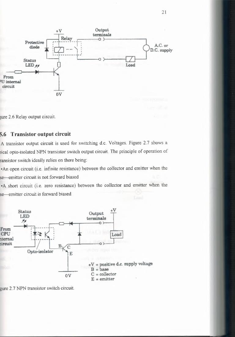
:.5.5 Relay output circuit Figure 2.6 illustrates thecircuit for a relay output interface. The NPN transistor is
ısed to switch current through the relay coil to close its contact. The internal circuit of
he PLC controls the transistor. The diode is connected across the relay coil to protect
he transistor from the effects of back e.m.f. This is the reverse voltage developed in the
elay coil, which causes an inductive current, which opposes the normal flow of current.
soth AC. and D.C. supplied loads can be connected through the relay output terminals.
21
A.C. Ol"D.C. supply
Load
From>u internalcircuit
ov
~ure 2.6 Relay output circuit.
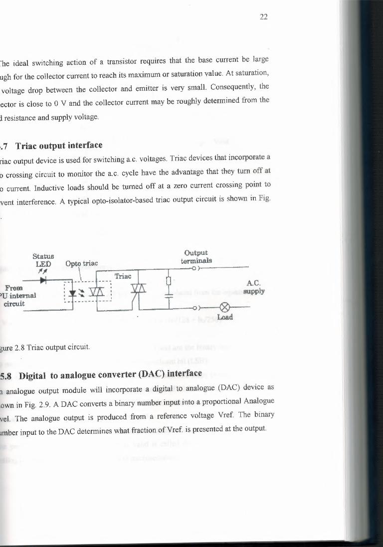
5.6 Transistor output circuitA transistor output circuit is used for switching d.c. Voltages. Figure 2.7 shows a
ıical opto-isolated NPN transistor switch output circuit. The principle of operation of
ransistor switch ideally relies on there being:
-An open circuit (i.e. infinite resistance) between the collector and emitter when the
se-emitter circuit is not forward biased
•A short circuit (i.e. zero resistance) between the collector and emitter when the
se-emitter circuit is forward biased
Status.LEDJ'!
~~ =:r-·. f -~--t--ı~ternal ~ ------ -~ı::ireuit . / B
Opto-isolator
Outputterminals
+V
CE
+V :; positive d,e, supply voltageB -base
OV C - collectorE -emitter
gure 2.7 NPN transistor switch circuit.
22
.he ideal switching action of a transistor requires that the base current be large
ugh for the collector current to reach its maximum or saturation value. At saturation,
voltage drop between the collector and emitter is very small. Consequently, the
ector is close to O V and the collector current may be roughly determined from the
i resistance and supply voltage.
:. 7 Triac output interface riac output device is used for switching a.c. voltages. Triac devices that incorporate a
o crossing circuit to monitor the a.c. cycle have the advantage that they tum off at
o current. Inductive loads should be turned off at a zero current crossing point to
vent interference. A typical opto-isolator-based triac output circuit is shown in Fig.
From ~Uintemal circuit
AC.supply
I I - O) ®--Load
gure 2.8 Triac output circuit.
5.8 Digital to analogue converter (DAC) interface G analogue output module will incorporate a digital to analogue (DAC) device as
ıown in Fig. 2.9. A DAC converts a binary number input into a proportional Analogue
vel. The analogue output is produced from a reference voltage Vref. The binary
ımber input to the DAC determines what fraction ofVref. is presented at the output.
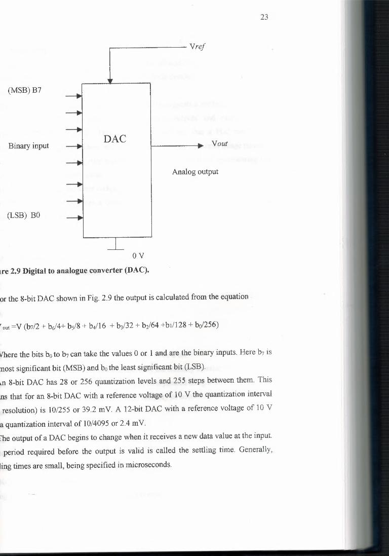
(MSB)B7
Binary input
(LSB) BO
23
-------- Vref
DAC Vout
Analog output
ovıre 2.9 Digital to analogue converter (DAC).
or the 8-bit DAC shown in Fig. 2.9 the output is calculated from the equation
rout =V (b1/2 + bı)4+ bs/8 + ba/Iô + b3/32 + b2/64 +bı/128 + bo/256)
vhere the bits bo to b1 can take the values O or 1 and are the binary inputs. Here b1 is
nost significant bit (MSB) and bo the least significant bit (LSB).
ın 8-bit DAC has 28 or 256 quantization levels and 255 steps between them. This
ns that for an 8-bit DAC with a reference voltage of 10 V the quantization interval
resolution) is 10/255 or 39.2 mV. A 12-bit DAC with a reference voltage of 10 V
a quantization interval of 10/4095 or 2.4 mV.
l'he output of a DAC begins to change when it receives a new data value at the input.
period required before the output is valid is called the settling time. Generally,
ling times are small, being specified in microseconds.
24
Input/output assignmentch input and output connection point on a PLC has an address used to identify the I/O
. Each manufacturer uses a proprietary identification system, which is related to the
ıe and number of input/output options possible.
The IEC 113 1-3 programming languages standard suggests a method for the direct
ıresentation of data associated with the inputs, outputs and memory of a
ıgrammable logic controller.' This is based on the fact that a PLC memory is
ganized into three regions. These are input image memory (I), output image memory
) and internal memory (M). Any memory location including those representing I/O
:s can be referenced directly using
(first letter code) (second letter code)(numeric field)
ıere the % character indicates a directly referenced variable. The first letter code
ecifies the memory region:
I = input memory
O = output memory
M = internal memory
ıe second letter code specifies how memory is organized:
X =bit
B =byte
W=word
D = double word
L = longword
If a second letter code is not given it is assumed to be a bit.
The numeric field component is used to identify the memory location. It supports the
mcept of I/O channels since numeric fields can be separated using a period.
Some examples of direct referencing of I/O memory as advocated in the IEC 1131-3
:andard are:
%Xl (* input memory bit 1 *)
%Il (* also input memory bit 1 *)
% 1B2 (* input memory byte 2 *)
%IX10.4 (* input byte address 10 bit 4 *)
%QK-1 (* output memory bit 1 *)
Jsing names that identify the purpose of each contact and coil in a ladder diagram aids
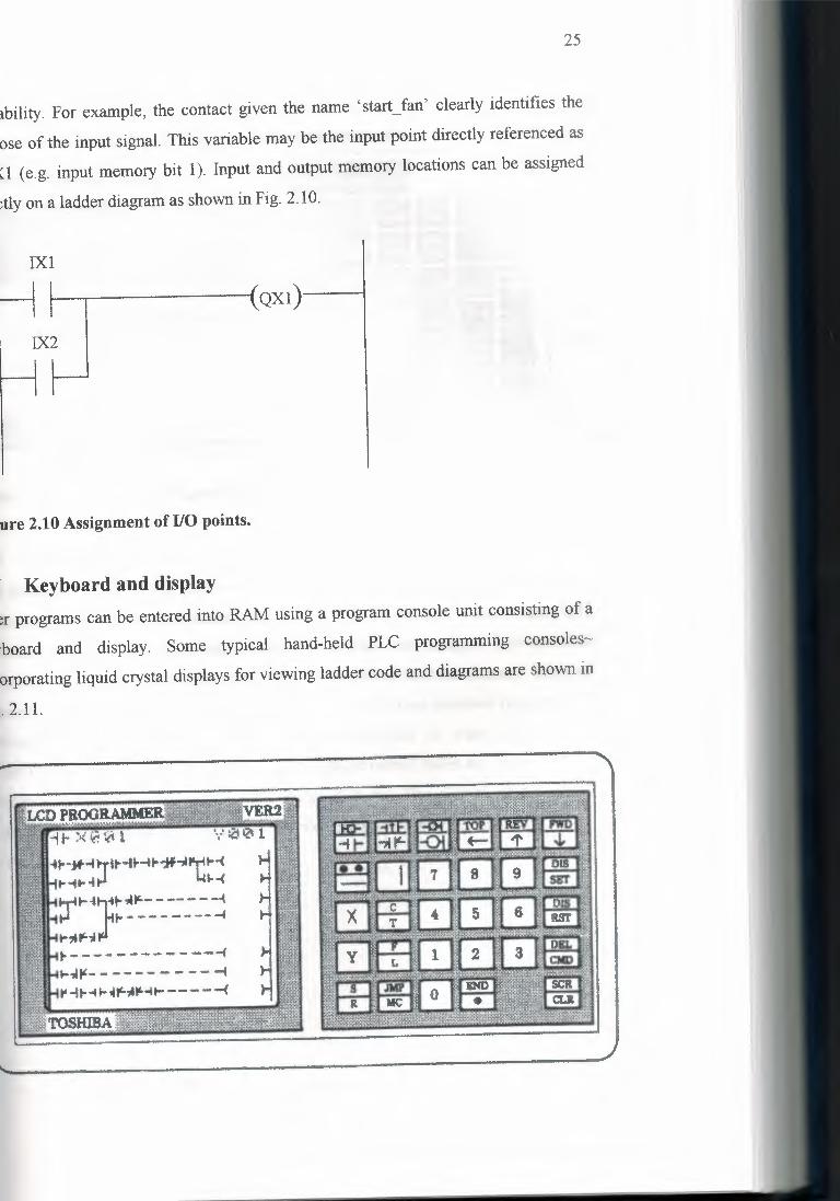
25
ability. For example, the contact given the name 'startfan' clearly identifies the
ose of the input signal. This variable may be the input point directly referenced as
a (e.g. input memory bit 1 ). Input and output memory locations can be assigned
.tly on a ladder diagram as shown in Fig. 2.10.
ure 2.1 O Assignment of 1/0 points.
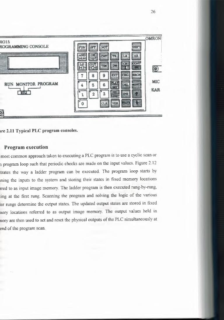
Keyboard and display!r programs can be entered into RAM using a program console unit consisting of a
rboard and display. Some typical hand-held PLC programming consoles
orporating liquid crystal displays for viewing ladder code and diagrams are shown in
,. 2.11.
R015ROGRAMMINGCONSOLE
RUN MONITOR PROGRAMI I JI IıJtJı ı
26
MIC
EAR
ıre 2.11 Typical PLC program consoles.
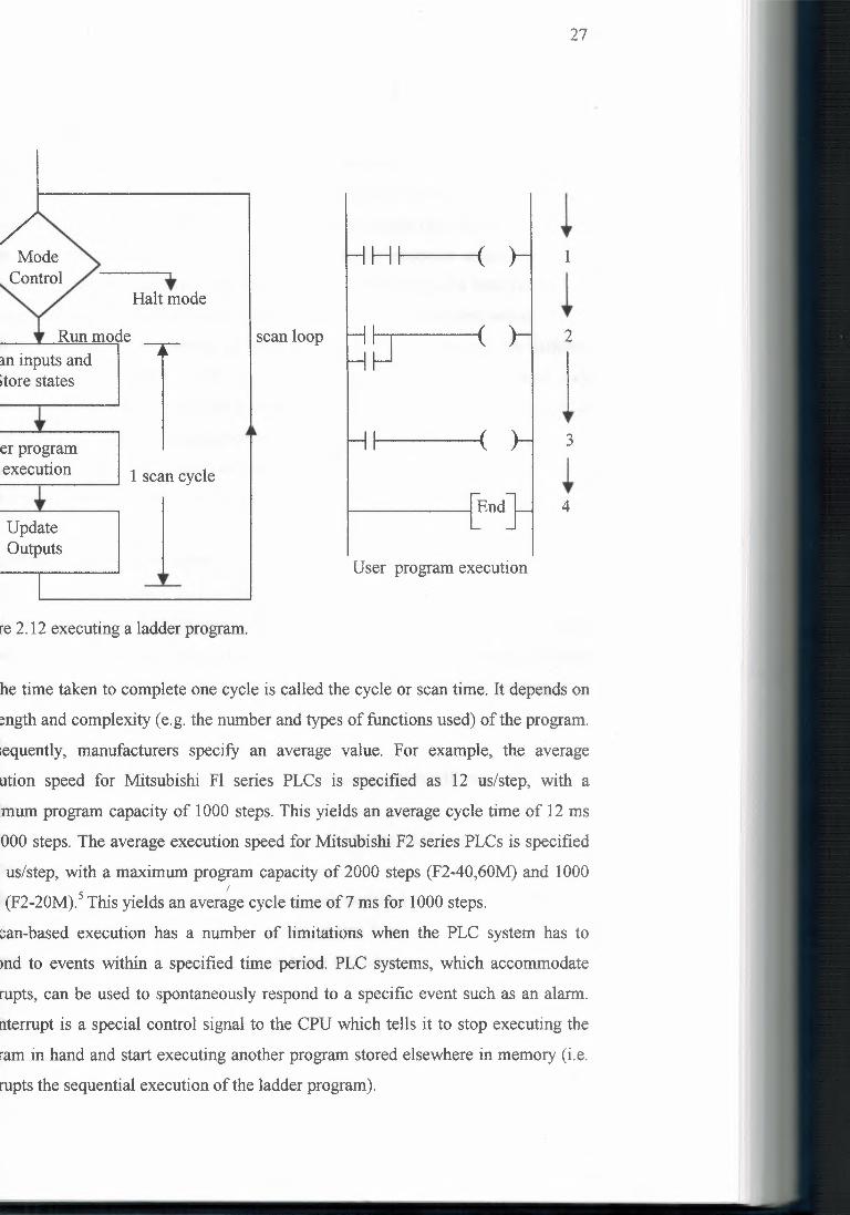
Program executionmost common approach taken to executing a PLC program is to use a cyclic scan or
ıı program loop such that periodic checks are made on the input values. Figure 2.12
:trates the way a ladder program can be executed. The program loop starts by
ming the inputs to the system and storing their states in fixed memory locations
rred to as input image memory. The ladder program is then executed rung-by-rung,
ting at the first rung. Scanning the program and solving the logic of the various
ler rungs determine the output states. The updated output states are stored in fixed
nory locations referred to as output image memory. The output values held in
nory are then used to set and reset the physical outputs of the PLC simultaneously at
end of the program scan.
27
Hl ( 1ı•Halt mode
Run modean inputs and,tore states
scan loop ( 2
ıI ( 3er program
execution
UpdateOutputs ı
ı4
1 scan cycle
User program execution
re 2.12 executing a ladder program.
he time taken to complete one cycle is called the cycle or scan time. It depends on
engthand complexity (e.g. the number and types of functions used) of the program.
ıequently, manufacturers specify an average value. For example, the average
ution speed for Mitsubishi Fl series PLCs is specified as 12 us/step, with a
mum program capacity of 1000 steps. This yields an average cycle time of 12 ms
000 steps. The average execution speed for Mitsubishi F2 series PLCs is specified
us/step, with a maximum program capacity of 2000 steps (F2-40,60M) and 1000I
, (F2-20M).5 This yields an average cycle time of 7 ms for 1000 steps.
can-based execution has a number of limitations when the PLC system has to
md to events within a specified time period. PLC systems, which accommodate
rupts, can be used to spontaneously respond to a specific event such as an alarm.
nterrupt is a special control signal to the CPU which tells it to stop executing the
ram in hand and start executing another program stored elsewhere in memory (i.e.
rupts the sequential execution of the ladder program).

28
Multitasking and multiprocessingneed PLC systems incorporate a processor scheduler to enable multitasking and
processing. Multitasking is the running of two or more tasks (also called
.sses) on a single processor such that they share processor time so that they appear
n in parallel. Different tasks of a program can be executed at different rates.
equently, time critical tasks (e.g. the monitoring of the state of a limit switch) can
vena high priority and scheduled to be executed within a fixed time period.
ultiprocessing is the running of tasks or processes simultaneously on different
ıssors. In this context a task or process is considered to be a separate code
ıent, which performs a discrete activity (a program organizational unit, or POU in
terminology). With a multiprocessing system, tasks such as 'closed loop PID
ortional, integral, derivative) control' and 'ladder circuit control' can be mapped
separate processors and run concurrently, communicating with one another.
10 Development systemsC development system would normally comprise a host computer connected via a
l communications RS232C port to a target PLC. The host computer provides a
rare environment to perform editing, file storage, printing and program operation
toring. Typically, the process of writing a program to run on the PLC consists of:
sing an editor to write/draw a source program
onverting the source program to binary object code which will run on the PLC's
ıcroprocessor
own loading the object code from the host PC to the PLC system via the serial
ımmunications port
fıe editor enables programs to be created and modified on the host computer in
r graphical form, such as a ladder diagram, or text form, such as mnemonic code.
ıres such as cut and paste, copy program block and address search are standard.
30
CHAPTER 3
Input devices
This chapter provides a brief overview of sensing devices used in manufacturing
ırocesses. Sensing devices with a digital output can be connected directly to the digital
ııput port of a PLC. Sensors, which produce an analogue voltage signal, are connected
ısing an analogue to digital converter.
3.1 Digital devicesThe operation of a PLC may be based on signals received from digital switching
levices, which detect an event occurring. For example, the presence of an object on a
.onveyor belt can be detected using a proxinııity switch or a photoelectric detector. Some
.ommonly used digital switching devices are described below.
3.1.1 Pressure and temperature switchesPressure switches monitor pressure and have a contact which changes state when a pre
ıet pressure threshold value is reached. When the pressure level falls below the threshold
.alue the contact resumes its initial position. Pressure switches are used in pneumatic and
ıydraulic applications.
Thermostats monitor temperatureand have a contact which changes state when a pre-set
emperature threshold value is reached. When the temperature value falls below tlııe
breshcld value the contact resumes its initial position. Thermostats are used in a wide
cınge of applications including tlııe temperature monitoring and control of machines and
eating installations. Many tlııermostats incorporate some hysteresis, which means that they
witch on and off at different temperatures. This is referred to as differential regulation
J •••• tween two threshold values.
3.1.2 Proximity switchesProximity switches are used for non-contact object detection. They integrate a Sensing

31
element and a transistor switch output circuit. The output changes state. When the object is
i~. th~. vifi.!Jtty qf tb}~ ~:nsor, element. Proximity switches.are.classified .as either inductive or
eapaeitive, which relates. to the type- of sensing technology used. Inductive· types are
suitable for detecting ferrous and non-ferrous metals.
. . ·ty
~
· .. ·ı·ve to proxunıSenser şensı J
. . . switen nı-Inductive {)roximity ·
~
. ·ey switeh nı-';tive proXlmı.Capacı ·
~
Frgure-3.1 The-IEC graphical symbols for proximity switches.
Capacitive types will sense the presence of almost any material. The TEC symbols used to
represent proximity switches are shown in Fig. 3.1.
The principle of operation of an inductive proximity switch is based on the generation of
an alternating magnetic field, which is affected by a metal object passing within its range.
_.\ typical device would have a sensing range of 2 mm and a switching speed of 800 Hz.
Toe principle of operation of a capacitive device is based on generating an electric field,
.hich is modified by any object passing within its range. A typical device would have a
sensing range of 1-1 O mm (adjustable) and a switching speed of 400 Hz.
The d.c. switching proximity devices are available with NPN open collector and PNP
open collector transistor output stages. Figure 3.2 illustrates how to connect an NPN
transistor output to a PLC sink input circuit and a PNP transistor output to a PLC source
32
input circuit.
3.1.3 Photoelectric switchesPhotoelectric devices consist of a light source and a photo-receiver incorporating a
transistor switch circuit.PNP and NPN transistor output devices are available.The ways in
which the light source and photo-receiver can be set up to detect objects are illustrated in
Fig. 3.3. Photoelectric switches are categorized as being either through beam, mirror
reflection,retro-reflectiveor diffusereflective.The through-beamtype of photoelectric system has a separate transmitter and receiver.
An object is detected when it breaks the light beam. The through-beam photoelectric
detector can be used for long-rangesensing.A typical device would have a sensingrange of
8000mm.A plane surface mirror can be used to reflect back the transmitted light beam to the
receiver.In this case, the object is detectedwhen the reflectedbeam is broken. With a plane
mirror reflector, the transmitter and receiver must be mounted such that the angle of
incidenceequals the angle of reflection.The retro-reflective type of photoelectric switch uses a special type of reflector which
eturns transmitted incident light back in the same direction from which it was sent. This
allows the transmitter and receiver to be incorporated in the same housing. With proper
alignmentof the photoelectricdevice to the reflector a typical device would have a sensing
rangeof 2000 mm.If a parallelbeam of light is incidenton a sheet of paper the light is reflectedin
all directions because the surface is not perfectly smooth like that of a mirror. This is an
exampleof diffuse reflection. A diffuse reflective type of photoelectric switch contains a
:ransmitterand receiver in the same housing and switches when the diffuse reflection level
exceedsa thresholdvalue.A typicaldevicewould have a sensingrange of 100mm.
33
24Vd.e
,;:. Status LED
Proldmity @switch ;
NPN open !,,eellector :
Input terminal- • • connection
\
Sensing·element L--1...~-:::-----ı O . l
I :e ov!._ __ ,..,. __ ;,;,; ,. _
Proximityswitch .---~---~-----·•'+'
I I ı;::IPNPopen • J ccollector : ~ , :
24Vd.c
JSensingelement
q
-----·--· ı8
f1~; )t-To internal:~ f ~~CPU clrçuit
~ Status LED
ovb)
-gure 3.2 Connecting NPN and PNP transistor output proximity switches: (a) Sink input
uit connection and (b) source input circuit connection.
34
~ewIOO';lfiLing
rınss,
"Ranee----=
om~{ '"1- .•. _
Lightt.rnnımı;t.ıer
lalLıo4ıi
NOei•,er
LightNceiverMirror
reneetoı-
olLight
1ransmitter
(.cl
Lighttransmitter
reeeiver
Figure 3.3 (a) through beam (b) mirror reflection (c) retro-reflection (d) diffuse
flection
35
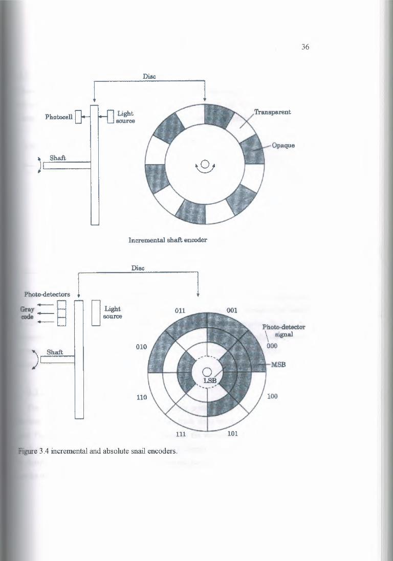
3.1.4 Optical switchesOptical encoders convert either translation or rotary displacement into digital
mformation. They operate by using a grating, which moves between a light source and
detector. There are two forms of optical encoder, namely incremental and absolute.
Incremental encoders produce a pulse for each resolvable change in position. Counting
oulses from some reference point can make a relative measurement of position. Absolute
encoders produce a unique coded number for each resolvable position.
An example of an incremental shaft encoder is shown in Fig. 3.4. The grating is a disc
with a single concentric track of evenly spaced opaque and transparent regions. When light
asses through a transparent region of the grating an output is obtained from the photo
etector. When the shaft is turned, the disc rotates and chops the light beam so that the
hoto-detector produces a series of electrical pulses. Position is measured by counting the
number of pulses generated by the photo-detector as the disc rotates from a reference point.
3y incorporating two tracks shifted by a quarter-cycle relative to one another and two
noto-detectors it is possible to produce two signals from which the direction of rotation
can be determined by noting which signal rises first. If a motor the pulse rate drives the
shaft of an incremental encoder is proportional to the motor's speed.
The disc of an absolute shaft encoder has several concentric tracks, with each track
ving an independent light source and photo-detector. With this arrangement a unique
inary or Gray coded number can be produced for every shaft position. The Gray code
anges by a single bit between successive positions (see Fig. 3.4). Table 3.1 compares the
Gray code with binary code. Resolution of an absolute encoder depends on the number of
tracks (bits). For example, a 3-bit binary output produces 2 or 8 resolvable positions.
Linear encoders use a grating in the form of a slide to make a measurement of "near
ovement. They may be of incremental or absolute type. Rotary and linear absolute
coders read actual position and unlike incremental encoders they do hot need a counting
vıce.
Photocell
36
Disc
ILi.ghtsource
1
Opaque
Incremental shaft encoder
Dise
Photo-deteetors IGray-§.eode ---
) Shaft
D Lightsource
l010
.Photo-detect.or\ signal000
MSB
110
- gure 3 .4 incremental and absolute snail encoders.
37
3.2 Analogue devicesMany applications involve monitoring analogue signals representing the variation of a
hysical quantity. For example, the variation of displacement can be measured using a
linearvariable differentialtransformer(LVDT),which convertsa position
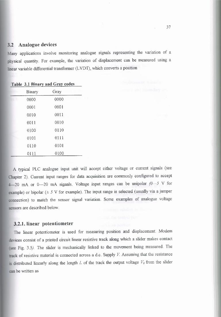
Table 3.1 Binary and Gray codes
Binary Gray
0000 0000
0001 0001
0010 0011
0011 0010
0100 0110
0101 0111
0110 0101
0111 0100
A typical PLC analogue input unit will accept either voltage or current signals (see
Chapter 2)..Current input ranges for data acquisition are commonlyconfigured to accept...-20 mA or 0-20 mA signals. Voltage input ranges can be unipolar (0-5 V for
example)or bipolar (± 5 V for example).The input range is selected (usuallyvia a jumper
onnection) to match the sensor signal variation. Some examples of analogue voltage
sensorsare describedbelow.
3.2.1. linear potentiometerThe linear potentiometer is used for measuring position and displacement. Modem
evices consist of a printed circuit linear resistive track along which a slider makes contact
see Fig. 3.5). The slider is mechanically linked to the movement being measured. The
:rack of resistive material is connected across a d.c. Supply V Assumingthat the resistance
- distributed linearly along the length L of the track the output voltage Vo from the slider
canbe writtenas
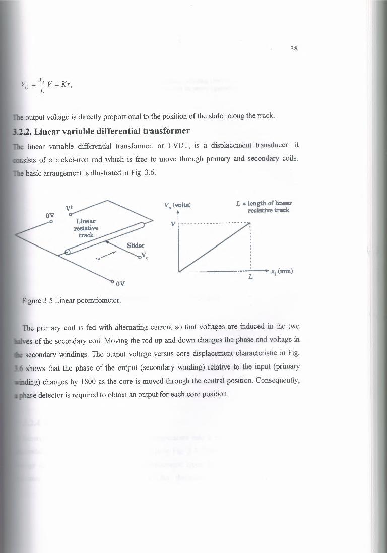
38
X· V0 ::::-1V::::Kx- L I
.ne output voltage is directly proportional to the position of the slider along the track.
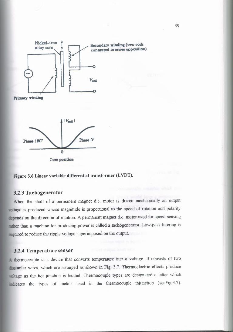
.2.2. Linear variable differential transformer:-he linear variable differential transformer, or LVDT, is a displacement transducer. It
sists of a nickel-iron rod which is free to move through primary and secondary coils.
e basic arrangement is illustrated in Fig. 3.6.
V0 (volts) L = length of linearresistive track
V
L xi (mm)
Figure 3 .5 Linear potentiometer.
The primary coil is fed with alternating current so that voltages are induced in the two
es of the secondary coil. Moving the rod up and down changes the phase and voltage in
secondary windings. The output voltage versus core displacement characteristic in Fig.
shows that the phase of the output (secondary winding) relative to the input (primary
ding) changes by 1800 as the core is moved through the central position. Consequently,
ase detector is required to obtain an output for each core position.
39
Nickel-ironalloy core Secondary windinı_ (two coils
connected in ıeriea opposition)
-PrimarY wiııdinı
I Vcmı I
oCore position
Figure 3.6 Linear variable differential transformer (LVDT).
3.2.3 TachogeneratorWhen the shaft of a permanent magnet d.c. motor is driven mechanically an output
Itage is produced whose magnitude is proportional to the speed of rotation and polarity
ends on the directionof rotation.A permanentmagnetd.c. motorused for speed sensing
raıherthan a machine for producing power is called a tachogenerator.Low-pass filteringis
...• quiredto reduce the ripplevoltage superimposedon the output.
3.2.4 Temperature sensorthermocouple is a device that converts temperature into a voltage. It consists of two
ssimilarwires, which are arranged as shown in Fig. 3.7. Thermoelectriceffects produce
ltage as the hot junction is heated. Thermocouple types are designated a letter which
icates the types of metals used in the thermocouple injunction (seeFig.3.7).
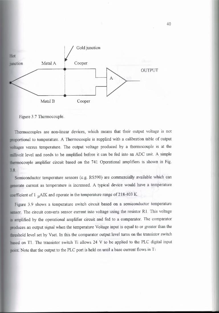
40
ti.on Metal A
V Gold junction
l CooperOUTPUT
MetalB Cooper
Figure3.7 Thermocouple.
Thermocouples are non-linear devices, which means that their output voltage is not
portional to temperature. A Thermocoupleis suppliedwith a calibration table of output
rages versus temperature. The output voltage produced by a thermocouple is at the
ivolt level and needs to be amplifiedbefore it can be fed into an ADC unit. A simple
ocouple amplifier circuit based on the 741 Operational amplifiers is shown in Fig.
Semiconductortemperature sensors (e.g. RS590) are commerciallyavailable which can
_ erate current as temperature is increased. A typical device would have a temperature
fficientof 1 µAIKand operate in the temperaturerange of 218-403K.
Figure 3.9 shows a temperature switch circuit based on a semiconductor temperature
or. The circuit converts sensor current into voltage using the resistor Rl. This voltage
..s amplifiedby the operational amplifier circuit and fed to a comparator. The comparator
oduces an output signalwhen the temperatureVoltage input is equal to or greater than the
eshold level set by Vset. In this the comparatoroutput level turns on the transistor switch
~ed on Tl. The transistor switch Ti allows 24 V to be applied to the PLC digital input
int. Note that the outputto the PLC port is held on until a base current flows in Tı
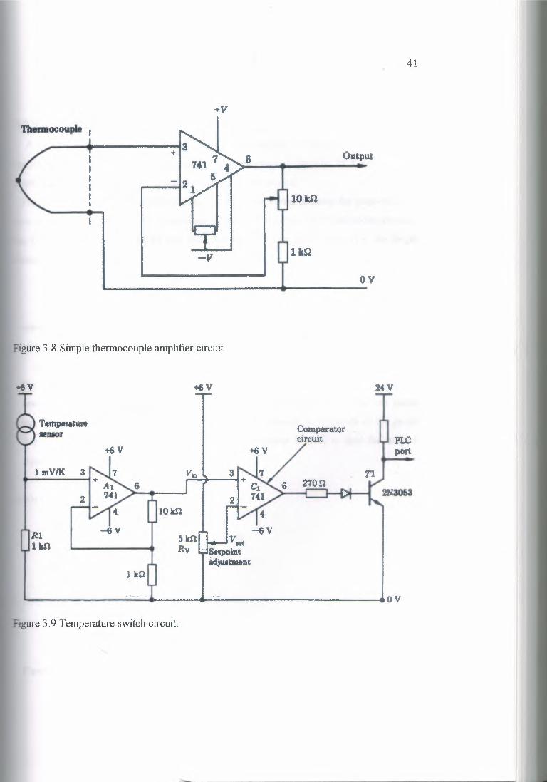
Thennocouple
+V
-v
41
6
ıoın
ov
Figure 3 .8 Simple thermocouple amplifier circuit
+6V
Temı,uaıure:ıemor
+6V
lmV/K
Rllkn
Figure 3 .9 Temperature switch circuit.
+6V
10:kn
5knRv
2-ıV
Comparat.orcircuit l'LC
port--6V

42
3.2.5 Strain gaugeA strain gauge is a transducer whose principle of operation is based on the variation of
resistance with dimensional displacement. A strain gauge is bonded to a surface of a
echanicalelement(e.g. a bar) in which strain is to be measured.Provided that the variation in length under loaded conditions is along the piige-sensitive
is an increase in load causes an increase in gauge resistance. The relationshipbetween
e change in resistance (ARIR) and the corresponding change in strain (i.e. the length
hange (,!JVL) is
MhG=-- M/ı
where G is called the gauge factor. -The gauge factor is about 2 for wire elementmetal
alloystraingauges and about 100 for semiconductorstrain gauges.A strain gauge is normally connected in a Whetstone bridge arrangementas shown in
Fig. 3 .1 O. The bridge is balanced under no load conditions so that any change in
resistance due to loadingunbalances the bridge and a signal is detected. A dummygauge
can be connected in the bridge to compensate for the change in resistance of the gauge
due to temperature variations. An instrumentationamplifier is used to feed the balance
signalto an ADC inputpoint.+V
straingauge._ ....-·
StandardresistorD.C supply
Figure 3.10 Strain gauge bridge.
------------- . ---
43
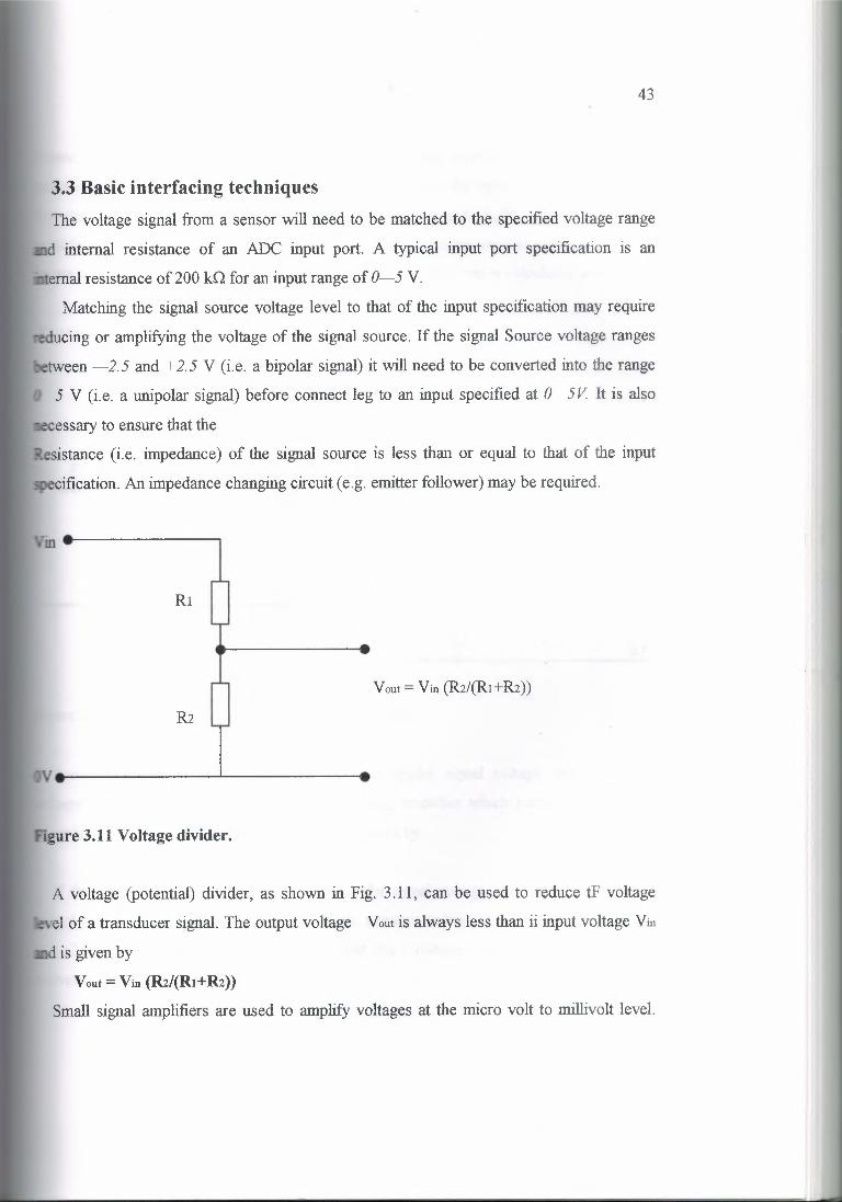
3.3 Basic interfacing techniquesThe voltage signal from a sensor will need to be matched to the specifiedvoltage range
d internal resistance of an ADC input port. A typical input port specification is an
emal resistance of 200 kO for an inputrange of 0-5 V.
Matching the signal source voltage level to that of the input specificationmay require
=ducing or amplifyingthe voltage of the signal source. If the signal Source voltage ranges
__tween -2.5 and +2.5V (i.e. a bipolar signal) it will need to be converted into the range
5 V (i.e. a unipolar signal) before connect leg to an input specified at O 5V It is also
~=cessaryto ensure that theesistance (i.e. impedance) of the signal source is less than or equal to that of the input
soecification.An impedancechangingcircuit(e.g. emitterfollower)may be required.
m
Rı
Vout = Vin (Rı/(Rı+Rı))
R2
ıgure 3.11 Voltage divider.
A voltage (potential) divider, as shown in Fig. 3.11, can be used to reduce tF voltage
·el of a transducer signal.The outputvoltage Vout is always less than ii inputvoltage Vin
dis givenby
Vout = Vin (Rı/(Rı+Rı))
Small signal amplifiers are used to amplifyvoltages at the micro volt to millivoltlevel.
44
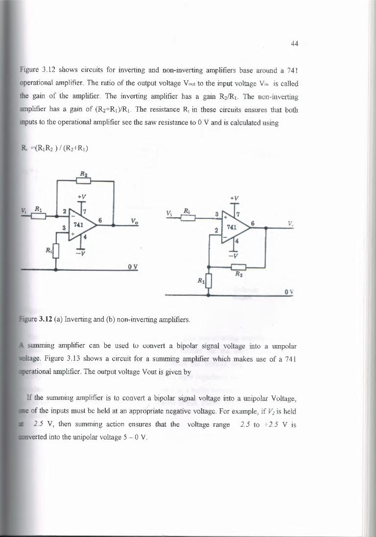
Figure 3.12 shows circuits for inverting and non-inverting amplifiers base around a 741
operational amplifier. The ratio of the output voltage Vout to the input voltage Vin is called
the gain of the amplifier. The inverting amplifier has a gain R2/R.1. The non-inverting
amplifier has a gain of (R2+Rı)/Rı. The resistance R, in these circuits ensures that both
mputs to the operational amplifier see the saw resistance to O V and is calculated using
Ri =(R1R2 ) I (R2+Rı)
+V +V
6 6 V,
-vOY
ov
Fıgure 3.12 (a) Inverting and (b) non-inverting amplifiers.
suınmıng amplifier can be used to convert a bipolar signal voltage into a umpolar
ltage. Figure 3.13 shows a circuit for a summing amplifier which makes use of a 741
. rational amplifier. The output voltage Vout is given by
If the summing amplifier is to convert a bipolar signal voltage into a unipolar Voltage,
of the inputs must be held at an appropriate negative voltage. For example, if Vı İs held
2.5 V, then summing action ensures that the voltage range 2.5 to +2.5 V is
verted into the unipolar voltage 5 - O V.
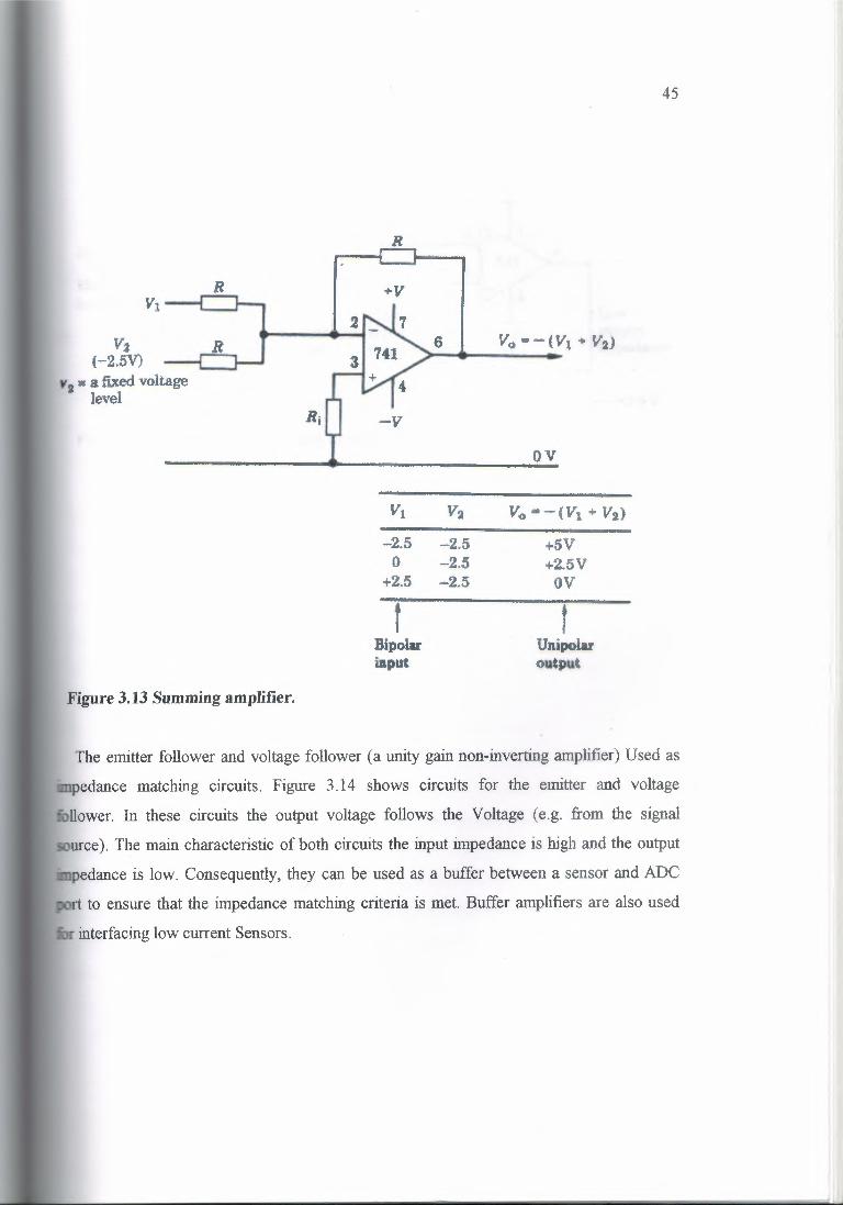
45
R
+V
V2(-2.5V)
v2 = a fixed voltagelevel
6
Ri'r'
OV
Vı Vı Vo s-(Vı + V2)
-2.5 -2.5 +5Vo -2.5 +2.5V
+2.5 -2.5 ov
f fBipolu Unipolarinput output
Figure 3.13 Summing amplifier.
The emitter follower and voltage follower (a unity gain non-inverting amplifier) Used as
:mpedance matching circuits. Figure 3 .14 shows circuits for the emitter and voltage
follower. In these circuits the output voltage follows the Voltage (e.g. from the signal
source). The main characteristic of both circuits the input impedance is high and the output
znpedance is low. Consequently, they can be used as a buffer between a sensor and ADC
rt to ensure that the impedance matching criteria is met. Buffer amplifiers are also used
interfacing low current Sensors.
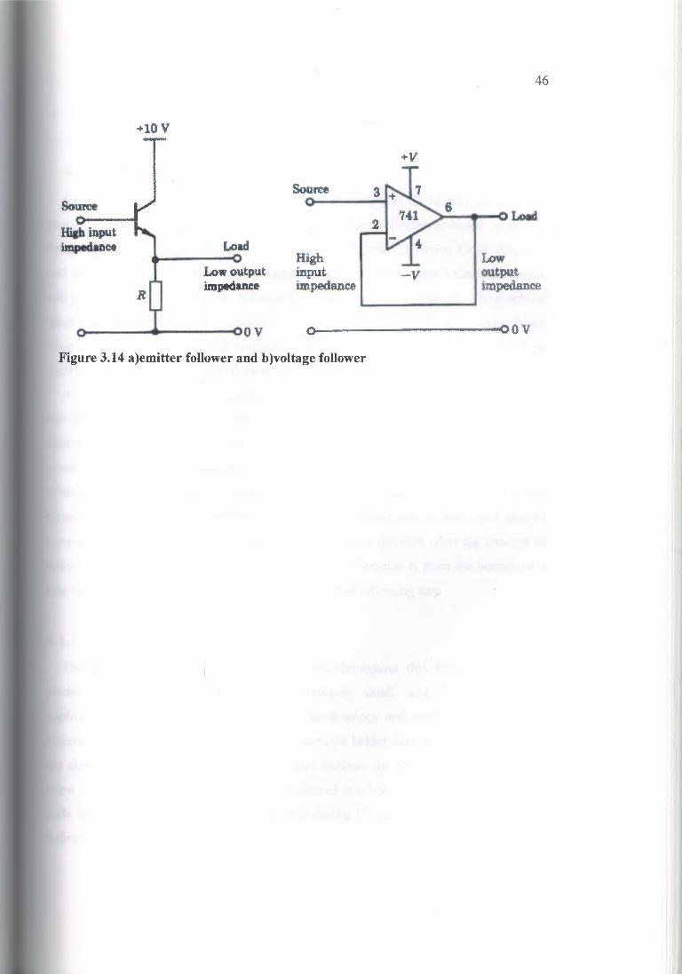
-ıo v,-+V T
SourceSouıı:e
~o
9 I 14ı>!oltigh inputimpedance l Load
---<> ffigh I ..L I LowLow output -v ~y impedance ~. ~tımpedanceımpedance
ov Q oov
46
Figure 3.14 a)emitter follower and b)voltage follower
47
CHAPTER4
Programming methods
4.1 Graphical languages
Graphical languages are widely .ıısed for programming PLCs as they are easy yet
powerful tools for developing control applications. Computer-based graphical
Programming packages exist for designing ladder diagrams, function block diagrams
and sequential function charts. These literally allow the user to draw a Control network
and provide a visual image of the solution to a particular control problem. The graphical
languages defined in the IEC standard are ladder diagram. (LD) and function block
diagram (FBD). Sequential function chart (SFC elements are also defined and can be
used in conjunction with either of these languages.
A circuit network can be considered as a set of interconnected graphical elements
representing a control plan. Graphical languages are used to represents the flow of a
onceptual quantity through a network. With a ladder diagram network the conceptual
quantity is power flow and the direction of power flow defined to be from left to right.
With a function block diagram network the concern of signal flow is applied and the
direction of signal flow is defined to be from the output side to the input side of
onnected function blocks or functions. With sequential function chart the concept of
activity flow is applied. Activity flow between SFC elements is from the bottom of a
step through the appropriate transition to the top of the following step.
4.1.1 Ladder diagram (LP)The ladder diagram method has been used throughout this book, as it is the
predominant programming method for developing small- and medium-scale PD
applications. The IEC standard is based on terminology and symbols as used b the
majority of current PLC systems. The IEC standard ladder diagram graphic- symbols
are shown in Table4.4. The standard includes symbols for SET RESET coils, which
allow a variable to be latched on, and then cleared at a late stage. Retentive coils (e.g.
oils whose Boolean states need to be held during PL power interruption) are also
efined.
48
Function blocks having Boolean inputs and outputs can be connected within ladder
diagram. Functions used in a ladder diagram may have an execution enable (EN) input
and an execution enable output (ENO). When EN is true the function is evaluated.
When EN is false it remains inactive. A ENO is taken high on if successful completion
of a function. It is possible to connect an ENO output to a EN of another function to
provide execution control.
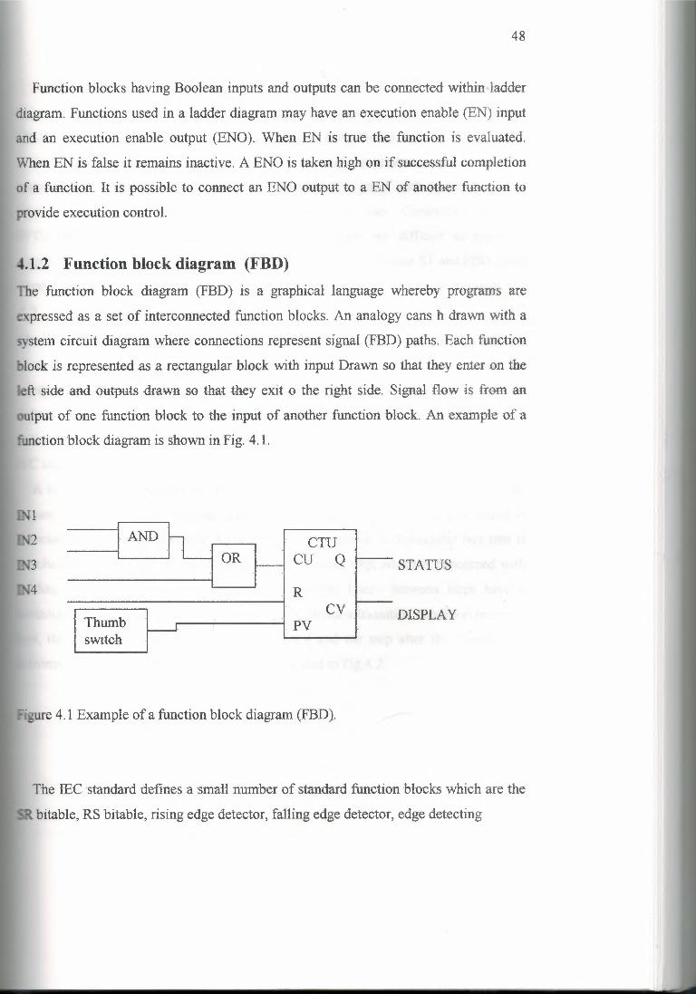
4.1.2 Function block diagram (FBD)The function block diagram (FBD) is a graphical language whereby programs are
expressed as a set of interconnected function blocks. An analogy cans h drawn with a
~ , stem circuit diagram where connections represent signal (FBD) paths. Each function
· lock is represented as a rectangular block with input Drawn so that they enter on the
eft side and outputs drawn so that they exit o the right side. Signal flow is from an
output of one function block to the input of another function block. An example of a
function block diagram is shown in Fig. 4.1.
l
.AND rL CTUcu Q. OR -R
CVThumb I PV1-----1- I
swıtch
STATUS
DISPLAY
Fıgure4.1 Example of a function block diagram (FBD).
The IEC standard defines a small number of standard function blocks which are the
.~bitable, RS bitable, rising edge detector, falling edge detector, edge detecting
49
inputs, tıp-counter, down-counter, up-down counter, pulse timer, on delay timer, off
delay timer and real-time clock. These are shown in Table 4.5. Other special purpose
blocks such as PID and ramp blocks can be designed usin_g the ST Ian_gua_ge.
The FBD language is suited to Boolean logic and continuous (e.g. closed-loop)
control applications. Although it is possible to construct a 'jump' within an FBD using a
label identifier, the IEC does not recommend its use. Constructs such as
IF/THEN/ELSE used with the structured text language are difficult to represent
graphically within an FBD. Consequently, direct translation between ST and FBD is not
always. possible.
4.2 Sequential function chart (SFC)The IEC I I31-3 standard describes the use of a graphical sequencing language referred
10 as the sequential function chart This is based on Grafceı, a graphical language for
developing sequential control programs, and defined as a French national standard.
Telemecanique PLCs use the Grafcet language but most major PLC systems provide an
ption for sequential programming. In fact, the IEC 1131-3 standard uses an existing
::EC standard to describe a graphical language for control sequences.
A sequence can be thought of as. a series of steps that occur in a defined order. The
sequential function chart language represents ea-ch step as a rectangular box, which is
ociated with a control action. An action can be drawn as a rectangular box that is
attached to a step. Every sequence starts with an initial step, which is concerned with
olding the system ready for operation. Connecting lines- between steps have a
· orizontal bar representing a transition condition. When a transition condition becomes
true, the step before the transition is deactivated and the step after the transition is
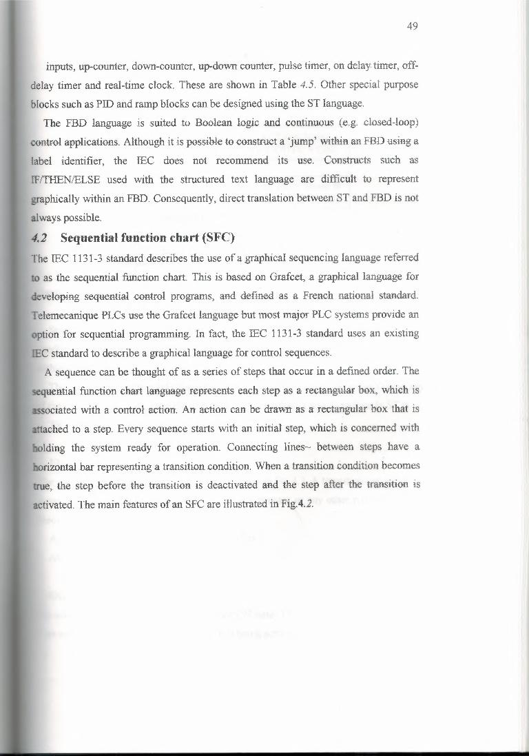
activated. The main features of an SFC are illustrated in Fig.4.2.
50
. INITAL· STEP
-:- Transition 1.N ACTION Name A· STRPl I ·{e.g.OUT1: =ON)
- .- Transition 2
N ACTION Name BI
STRP? -e.g, Om2: = ON)
_""" Transition 3
·N ACTION Name C_ISTFP1 (e.g. OUT3: = ON)
J
Figure 4. 2 Sequential function charts.
Steps are always separated by a transition and every transition must have a Boolean
ondition, which can be true. Every action and transition should be given a unique name
withina program.yThe software to implement transition conditions and actions can be written using any
f the IEC languages. An example of a transition condition (Trans 1) written in ST is
TRANSITION Transl:
: = Startbutton AND Ready;
END TRANSITIONThe same transition is shown as a Ladder Diagram in Fig.4.3. A transition can involve a
er (e.g. wait for an elapsed time to occur), a counter or any other type of function
block
An example of a simple action written in ST is
ACTIONName A
OUTl: =ON;
END ACTIONThe action called 'Name A' sets OUTl to an ON state. The action will occur as a result
f an associated step (e.g. STEP 1 in Fig. 4.2) being activated.
51
An action can have a qualifier, which determines the way in which the action will be
executed. An action qualifier is drawn as a rectangular box attached to the left hand side
of an action as shown in Figure 4.2. Commonly used qualifiers are N (none), S (set) and
R (reset). An N qualifier specifies that the action is executed only while the step is
active. An S (set) qualifier specifies that the action is to be latched on. The step acts as a
trigger for the latch and the action is said to be
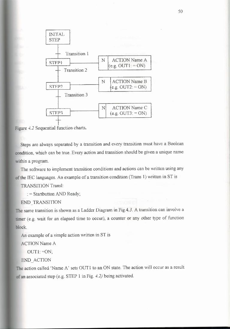
TRANSITION Trans 1
Startbutton ReadyH ı (Transı, ı
TRANSITION- .
figure 4.3 Ladder diagram transition expression.
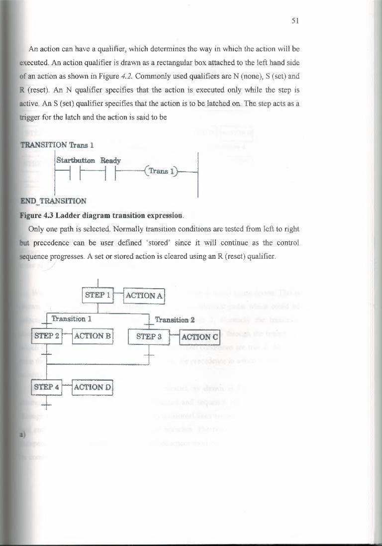
Only one path is selected. Normally transition conditions are tested from left to right
ut precedence can be user defined 'stored' since it will continue as the control
sequenc;İogresses. A set or stored action is cleared using an R (reset) qualifier.
ACTION A
·Transition 2
ACTIONB ACTIONC
STEP4 ACTIOND
52
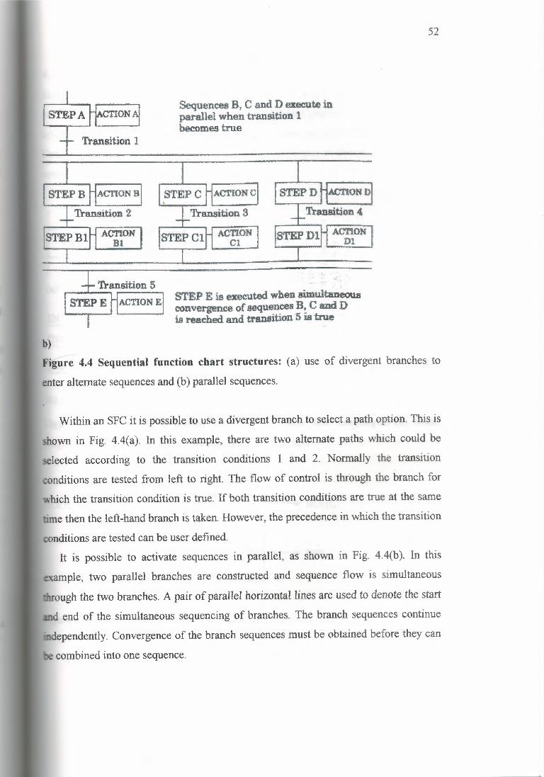
Sequences B, C and D execute inparallel when transition 1becomes true
STEP A
Transition l
Transition 2
ACTIONBl
AcrIONC
Transition 3
ACTIONCl
~ -~:.:
STEP E is executed when simultaneousconvergence of sequences B, C and Dis reached and tTanSition ·5 is tnıe
b)Fi~ 4.4 Sequential function chart structures: (a) use of divergent branches to
enter alternate sequences and (b) para11el sequences.
Within an SFC it is possible to use a divergent branch to select a path option. This isIshown in Fig. 4.4(a). In this example, there are two alternate paths which could be
selected according to the transition conditions 1 and 2. Normally the transition
conditions are tested from left to right. The flow of control is through the branch for
hich the transition condition is true. If both transition conditions are true at the same
time then the left-hand branch is taken. However, the precedence in which the transition
conditionsare tested can be user defined.It is possible to activate sequences in parallel, as shown in Fig. 4.4(b). In this
example, two parallel branches are constructed and sequence flow is simultaneous
ough the two branches. A pair of parallel horizontal lines are used to denote the start
d end of the simultaneous sequencing of branches. The branch sequences continue
dependently. Convergence of the branch sequences must be obtained before they can
combined into one sequence.

53
4.3 Translating between languagesSimple ladder rungs involving combinational logic can usually be translated into FBD
or ST, as illustrated in Fig. 4.5. The IEC 1131-3 standard specifies the operation of the
up-counter, down-counter and up-down counter in terms of an ST language algorithm.
Consider the function block representation of the up-counter as shown in Fig. 4.6. The
operation of the up-counter function block can be .
(a)
1
IN2 OR f ;AND CRl
3
)
figure 4.5 Translating a ladder diagram into other me languages: (a) ladder
· agram, (b) function block diagram and (c) structured text.
CTUOOL ----i R..:TRJG BOOL Qt • BOOLcu
BOOL RINT .. PV CV
Figure4.6 Up-counter function block.
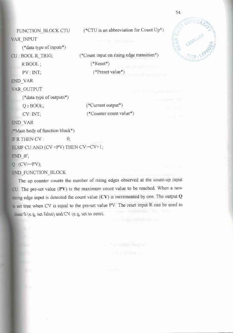
FUNCTION BLOCK CTU
AR INPUT
(*data type of inputs*)
CU: BOOLR_TRIG;
R:BOOL;
PV: INT;
END VAR
AR OUTPUT
(*data type of outputs*)
Q: BOOL;
CV: INT;
END VAR
"Main body of function block*)
O; R THEN CV:
54
(*CTU is an abbreviation for Count Up*)
(*Count input on rising edge transition*)
(*Reset*)
(*Preset value")
(*Current output*)
(*Counter count value*)
ELSIFCU AND (CV <PV) THEN CV:=CV+1;
.8ID_IF;
: (CV>=PV);
~ FUNCTION BLOCK- -
The up counter counts the number of rising edges observed at the count-up input
. The pre-set value (PV) is the maximum count value to be reached. When a new
sing edge input is detected the count value (CV) is incremented by one. The output Q
- set true when CV is equal to the pre-set value PV. The reset input R can be used to
.ea1 \) \e.ı. <::,e,\ fa\<::,e') al\u. C,'J \e.ı. <::,e,\ \() 'Le1()).
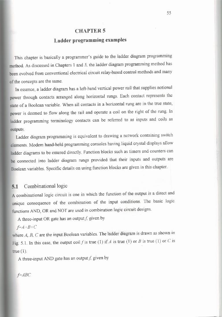
55
CHAPTERS
Ladder programming examples
This chapter is basically a programmer's guide to the ladder diagram programming
method. As discussed in Chapters 1 and 5, the ladder diagram programming method has
een evolved from conventional electrical circuit relay-based control methods and many
of the concepts are the same.In essence, a ladder diagram has a left-hand vertical power rail that supplies notional
power through contacts arranged along horizontal rungs. Each contact represents the
state of a Boolean variable. When all contacts in a horizontal rung are in the true state,
power is deemed to flow along the rail and operate a coil on the right of the rung. In
ladder programming terminology contacts can be referred to as inputs and coils as
outputs.-:
Ladder diagram programming is equivalent to drawing a network containing switch
elements. Modem hand-held programming consoles having liquid crystal displays allow
adder diagrams to be entered directly. Function blocks such as timers and counters can
be connected into ladder diagram rungs provided that their inputs and outputs are
Boolean variables. Specific details on using function blocks are given in this chapter.
5.1 Combinational logicA combinational logic circuit is one in which the function of the output is a direct and
unique consequence of the combination of the input conditions. The basic logic
functions AND, OR and NOT are used in combination logic circuit designs.
A three-input OR gate has an output/, given by
f=A+B+C
whereA, B, C are the input Boolean variables. The ladder diagram is drawn as shown in
Fig. 5 .1. In this case, the output coil f is true (1) if A is true (1) or B is true (1) or C is
true (1).A three-input AND gate has an output/, given by
f=ABC
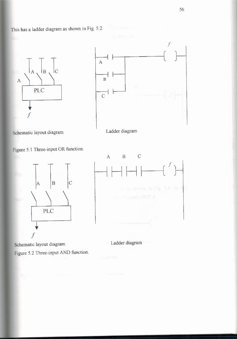
This has a ladder diagram as shown in Fig. 5.2.
A
PLC
f
Schematic layout diagram
Figure 5.1 Three-input OR function.
PLC
+f
Schematic layout diagram
Figure 5.2 Three-input AND function.
A
f
B
56
C
Ladder diagram
A B C
Ladder diagram
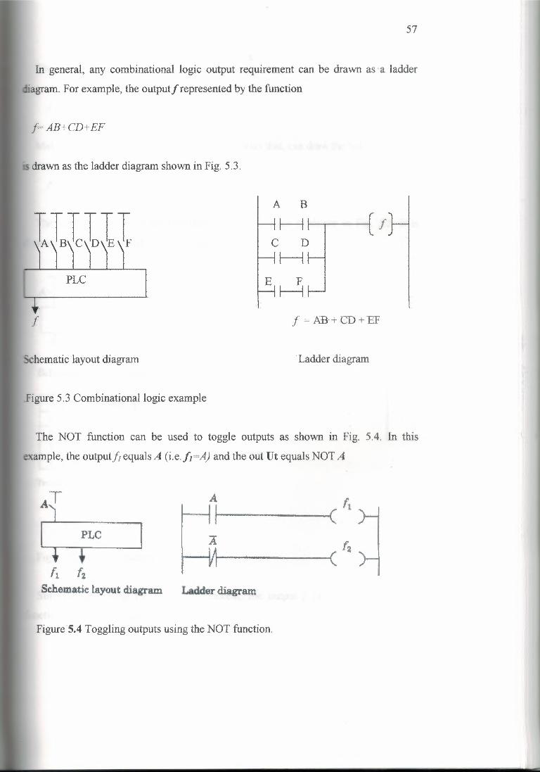
57
In general, any combinational logic output requirement can be drawn as a ladder
iagram. For example, the output/represented by the function
f=AB+CD+EF
- drawn as the ladder diagram shown in Fig. 5.3.
A B
1--f --c D 1--f
I
PLC
I f =AB-+CD+EF
Schematic layout diagram · Ladder diagram
Figure 5.3 Combinational logic example
The NOT function can be used to toggle outputs as shown in Fig. 5.4. In this
example, the output/I equals A (i.e.fı=A) and the out Ut equals NOT A
A fı~ ~ı (ı. f2
Schematic layout diagram Ladder diagram
FigureSia Toggling outputs using the NOT function.

58
The output/ of a two-input NAND function is given by
f=AB
Making use ofDe Morgan's theorem, which states that, can draw the ladder diagram
f=AB=A+B
The ladder diagram for the two-input NAND function is shown in Fig. 5.5. It is
drawn as NOTA in parallel (i.e. OR) with NOT B.
PLC
ff
Schematic layout diagram
A B f=AB o o 1o 1 1 1 o 1l 1 o Ladder diagram
Truth t..RhlA
Figure 5.5 NAND ladder diagram.
Similarly, by using De Morgan's theorem, the output f of the two-input NOR
function can be written as
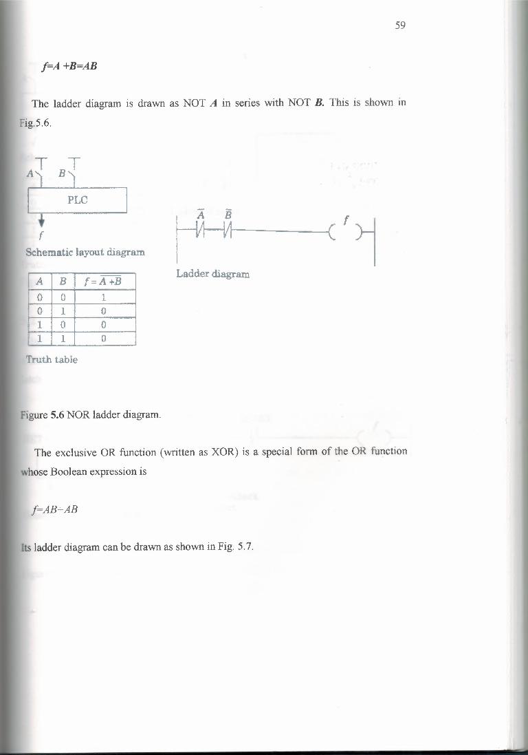
59
f=A+B=AB
The ladder diagram is drawn as NOT A in series with NOT B. This is shown in
Fig.5.6.
PLC
fSchematic layout diagram
A B f=A+Bo o 1o I o
' 1 o oI ı 1 o
Ladder diagram
Truth table
Figure 5.6 NOR ladder diagram.
The exclusive OR function (written as XOR) is a special form of the OR function
vhose Boolean expression is
f=AB+AB
ts ladder diagram can be drawn as shown in Fig. 5.7.
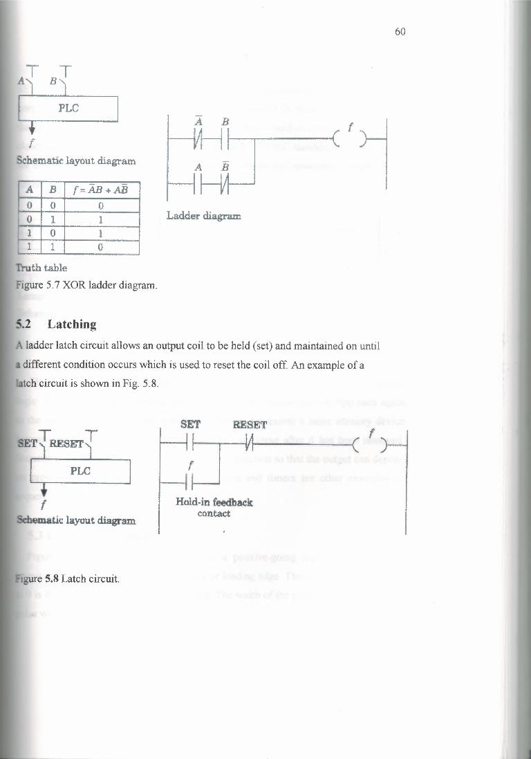
60
PLC A B f
fSchematic layont diagram A B
A B f=AB+ABo o oo 1 1ı o l1 1 o
Ladder diagram
Truth tableFigure 5.7 XOR ladder diagram.
5.2 Latchingn. ladder latch circuit allows an output coil to be held (set) and maintained on until
a different condition occurs which is used to reset the coil off. An example of a
latch circuit is shown in Fig. 5.8.
SET RESETf
PLC f
fematicl~out diagram
Hold-in feedbackcontact
rıgure 5.8 Latch circuit.
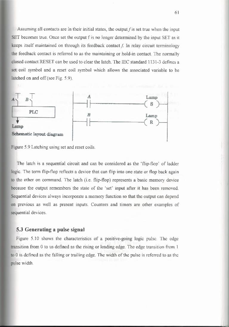
61
Assuming all contacts are in their initial states, the output f is set true when the input
SET becomes true. Once set the output f is no longer determined by the input SET as it
keeps itself maintained on through its feedback contact f In relay circuit terminology
the feedback contact is referred to as the maintaining or hold-in contact. The normally
closed contact RESET can be used to clear the latch. The IEC standard 1131-3defines a
set coil symbol and a reset coil symbol which allows the associated variable to be
latched on and off (see Fig. 5.9).
A Lamp I '! C s
PLC B Lamp ~· ~ı ( R Lamp Schematic layout diagram
Figure 5.9 Latching using set and reset coils.
The latch is a sequential circuit and can be considered as the 'flip-flop' of ladder
ogic. The term flip-flop reflects a device that can flip into one state or flop back again
to the other on command. The latch (i.e. flip-flop) represents a basic memory device
ecause the output remembers the state of the 'set' input after it has been removed.
Sequential devices always incorporate a memory function so that the output can depend
on previous as well as present inputs. Counters and timers are other examples of
sequential devices.
5.3 Generating a pulse signal Figure 5 .1 O shows the characteristics of a positive-going logic pulse. The edge
rransition from O to us defined as the rising or leading edge. The edge transition from 1
to O is defined as the falling or trailing edge. The width of the pulse is referred to as the
ulse width.
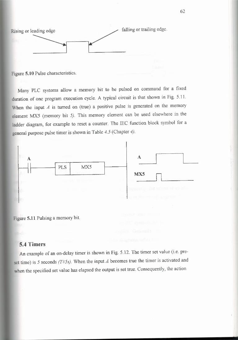
62
Risingor les ~ fallingor trailingedge
Figure 5.10 Pulse characteristics.
Many PLC systems allow a memory bit to be pulsed on command for a fixed
duration of one program execution cycle. A typical circuit is that shown in Fig. 5.11.
When the input A is turned on (true) a positive pulse is generated on the memory
element MX5 (memory bit 5). This memory element can be used elsewhere in the
ladder diagram, for example to reset a counter. The IEC function block symbol for a
general purpose pulse timer is shown in Table 4.5 (Chapter 4).
A
I PLS MX5
A
MX5 n.__ _
Figure 5.11 Pulsing a memory bit.
5.4 Timers An example of an on-delay timer is shown in Fig. 5.12. The timer set value (i.e. pre
set time) is 5 seconds (T#5s). When the input A becomes true the timer is activated and
hen the specified set value has elapsed the output is set true. Consequently, the action
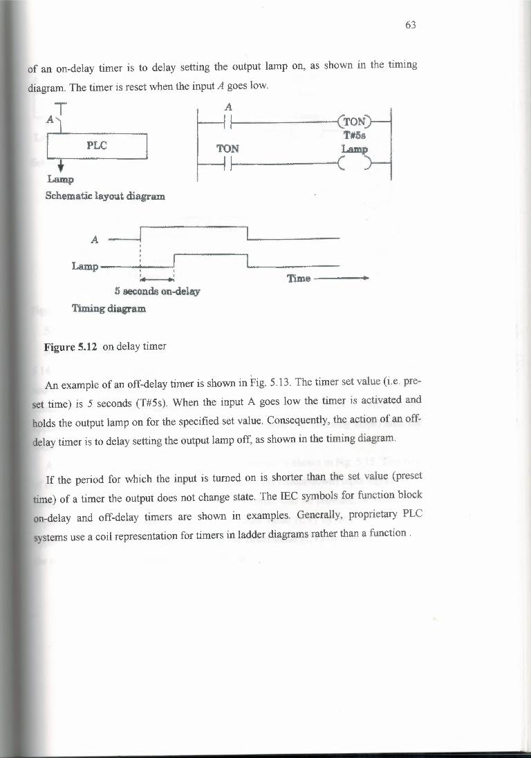
63
of an on-delay timer is to delay setting the output lamp on, as shown in the timing
diagram. The timer is reset when the input A goes low.
PLC
A ı---; r-1 ----~ (TON
TON T#5sı..-.....l I (Lamp
Lamp Schematic layout diagram
A
Lamp I I
I I
••• ••5 seconds on-delay
Timing diagram
Time---•
Figure 5.12 on delay timer
An example of an off-delay timer is shown in Fig. 5.13. The timer set value (i.e. pre
set time) is 5 seconds (T#5s). When the input A goes low the timer is activated and
holds the output lamp on for the specified set value. Consequently, the action of an off
delay timer is to delay setting the output lamp off, as shown in the timing diagram.
If the period for which the input is turned on is shorter than the set value (preset
time) of a timer the output does not change state. The IEC symbols for function block
on-delay and off-delay timers are shown in examples. Generally, proprietary PLC
ystems use a coil representation for timers in ladder diagrams rather than a function .
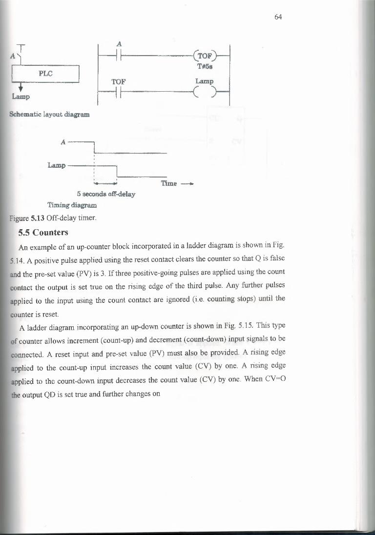
64
TA
A
}PLC
TOF l--1 j LampCLamp
Schematic layout diagram
A----.
Lamp
•• ••• Time ---ı,.5 seconds off-delay
Timing diagram
Figure 5.13 Off-delay timer.
5.5 CountersAn example of an up-counter block incorporated in a ladder diagram is shown in Fig.
5. 14. A positive pulse applied using the reset contact clears the counter so that Q is false
and the pre-set value (PV) is 3. If three positive-going pulses are applied using the count
ontact the output is set true on the rising edge of the third pulse. Any further pulses
applied to the input using the count contact are ignored (i.e. counting stops) until the
counter is reset.A ladder diagram incorporating an up-down counter is shown in Fig. 5. 15. This type
of counter allows increment (count-up) and decrement (count-down) input signals to be
connected. A reset input and pre-set value (PV) must also be provided. A rising edge
pplied to the count-up input increases the count value (CV) by one. A rising edge
pplied to the count-down input decreases the count value (CV) by one. When CV=O
the output QD is set true and further changes on
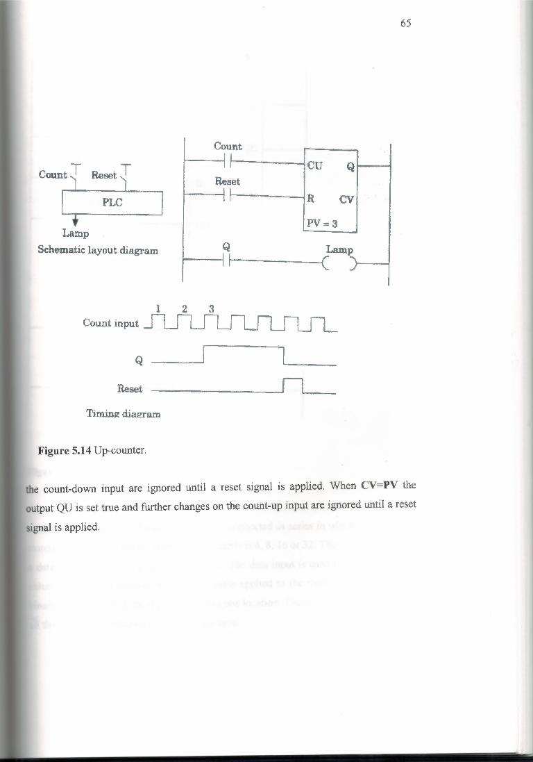
65
Count
Res
'
cu Qet
I R CV
py,,,,3
LampC
Count J Reset TPLC
LampSchematic layoutdiagram Q
l I ı
1 2 3Count input
Q
Reset
Timing diazram
Figure 5.14 Up-counter.
the count-down input are ignored until a reset signal is applied. When CV=PV the
output QU is set true and further changes on the count-up input are ignored until a reset
signal is applied.
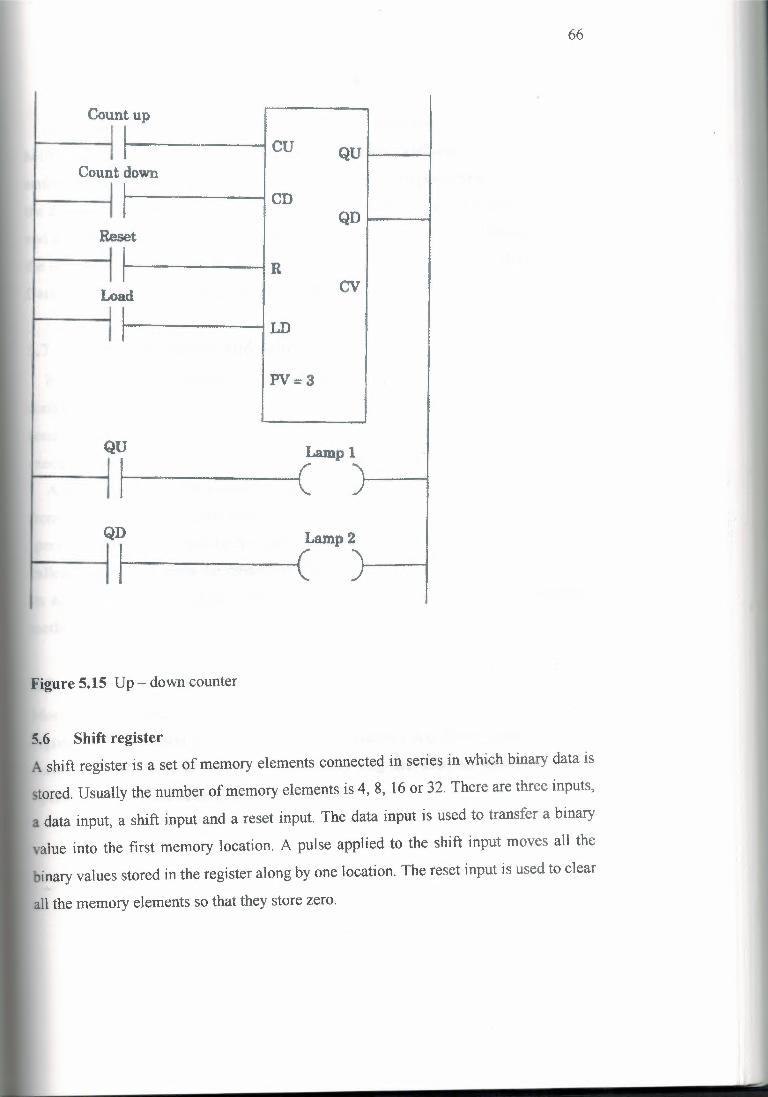
66
Count up I
Countdown cu QU• .
I I ICD
Reset QD,
IR
Load
'CV
JILD
PV::: 3
QU Lamp 1
I CQD Lamp2
I C
Figure 5.15 Up- down counter
5.6 Shift register A shift register is a set of memory elements connected in series in which binary data is
stored. Usually the number of memory elements is 4, 8, 16 or 32. There are three inputs,
a data input, a shift input and a reset input. The data input is used to transfer a binary
value into the first memory location. A pulse applied to the shift input moves a11 the
inaryvalues stored in the register along by one location. The reset input is used to clear
all the memory elements so that they store zero.
67
An example of a 4-bit shift register consisting of memory elements MlOO, Ml Ol,
M102 and M103 is shown in Fig. 5.16. The first memory element MlOOhas the same
state as the data input contact on Ii. The rising edge of a shift pulse input signal shifts all
the data in the register one bit to the left. Assuming the shift register is initially cleared
and a logic 1 is entered into MlOO a shift pulse moves the logic 1 into Ml Ol. Note that
the memory elements MlOO to M103 are used to drive the output coils Q400 to Q403.
Data in the last memory location of the register is lost when a shift is applied.
5. 7 Conditional jumps and subroutines It can be required that part of a ladder program has to be inactive when an input
condition occurs. A 'jump' function block can be used to skip ladder rungs on the
condition that a contact is made. When a contact is turned on the cyclic scan does not
execute ladder rungs betweenjump and end-jump labels marked on a ladder diagram.
A subroutine represents a complete ladder program which can be called repeatedly
from a main ladder program when required. A subroutine is implemented using a
special function coil for calling the routine in the ladder circuit. When the subroutine is
alled the processor scans the subroutine and returns control to the main program when
its actions have been completed. Details of implementation of jumps and subroutine
methods are manufacturer specific.
5.8 Arithmetic functions Most PLCs are able to do simple binary arithmetic operations with data stored in
egisters using function blocks to add, subtract, multiply and divide binary and BCD
numbers. Instructions to set and clear a carry flag are used as binary arithmetic
operations make use of a carry in their results

68
Schematic layoutdiagram
Data I Shift TReset T
PLC
Q400 Q401 Q402 Q403
Ladderdiagraın
MlOO Ml Ol M102 M103
Datainput ı-{) ı o 1 ol o I~
Shift
Memoryelements
Itı-------...-.1 L Data input MlOO
f (
Shift input --l SFT I MlOO12
13 Reset inputı-----ı ı----------ı ssr: MlOO
MlOO Q400
I CMl01 Q401
I -(
M102 Q402
1 {
M103 Q403
I {
Figure-5.16 A- 4 bit shift register
69
CHAPTER6
Tutorial examples
The aim of this chapter is to provide some further programming techniques useful for
applications. The areas covered include simple minimization of a Boolean equation
derived from a truth table, sequencing using timers, a cyclic timer circuit and a cyclic
shift register circuit.
6.1 Deriving a ladder diagram from a truth table In general, any combinational logic process can be described by a truth table, which
lists the logic values of the outputs for all possible combinations of the input. A truth
table with one output and n inputs consists of 2 - 8 rows. For example, a truth table with
three inputs has 2 or 8 rows.Given a truth table, an output function can be derived by one of two methods called
the sum-of-products method and the product-of-sums method. The sum-of-products
method is applied using the following rules:
1. Pick out all the rows that contain a logic 1 in the output column.
2 .For each row that has an output equal to logic 1, logically AND the corresponding
inputs3. Together using a negation whenever an input is zero. Take all the row products and
OR them together.
For example, consider the truth shown in Table 6. 1, where A, Band Care the
Boolean inputs to the PLC and f is the output coil to be energized according to the truth
table. Applying the sum-of-products method the output is given by
f=ABC +ABC +ABC
This can be drawn as a ladder diagram as shown in Fig. 6. 1.
This expression can be reduced to a simpler form by applying the laws ofBoolean
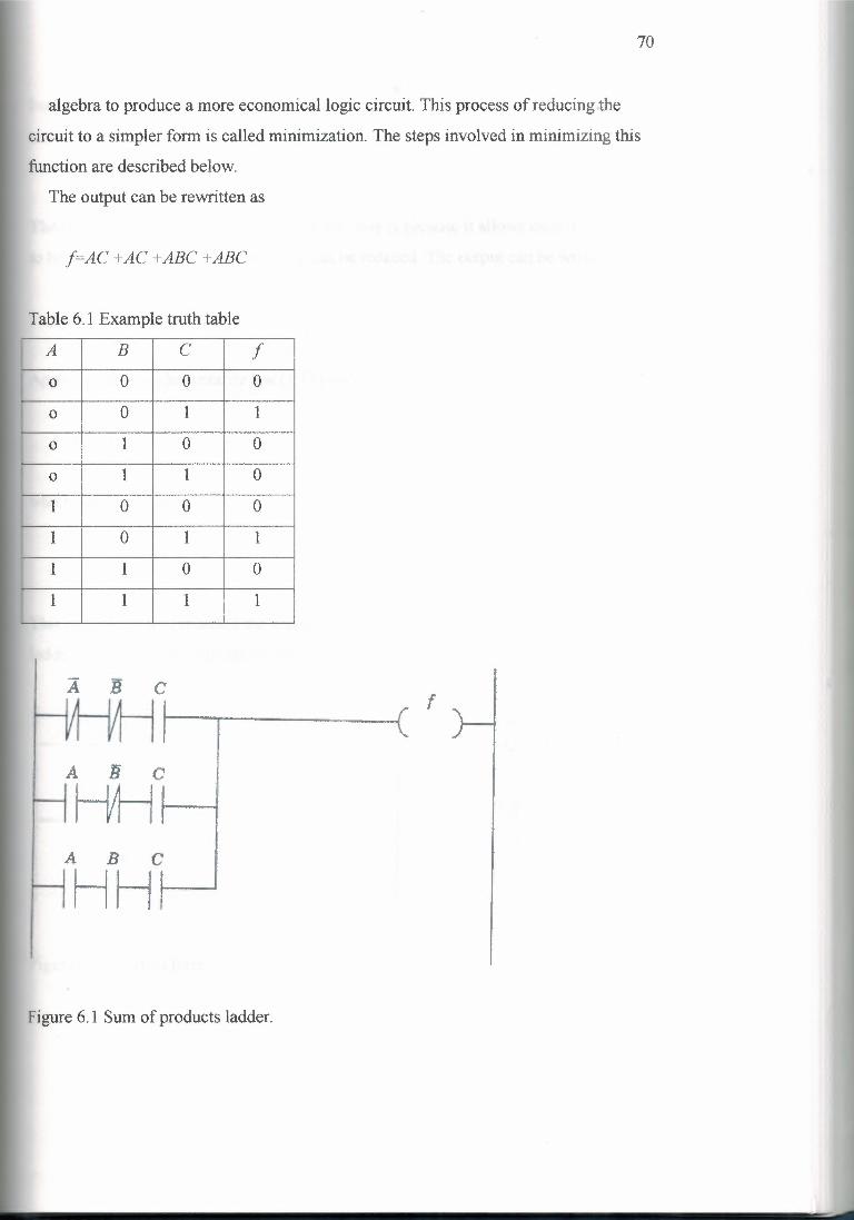
70
algebra to produce a more economical logic circuit. This process of reducing the
circuit to a simpler form is called minimization. The steps involved in minimizing this
function are described below.
The output can be rewritten as
f=AC +AC +ABC +ABC
Table 6.1 Example truth table
IA B C f
Io o o o
Io o 1 1
Io 1 o o
Io 1 1 o
I1 o o o
I1 o 1 1
I1 1 o o
I1 1 1 1
A B Cf
A 1J C HH, I
A B C
HHf I
Figure 6.1 Sum ofproducts ladder.
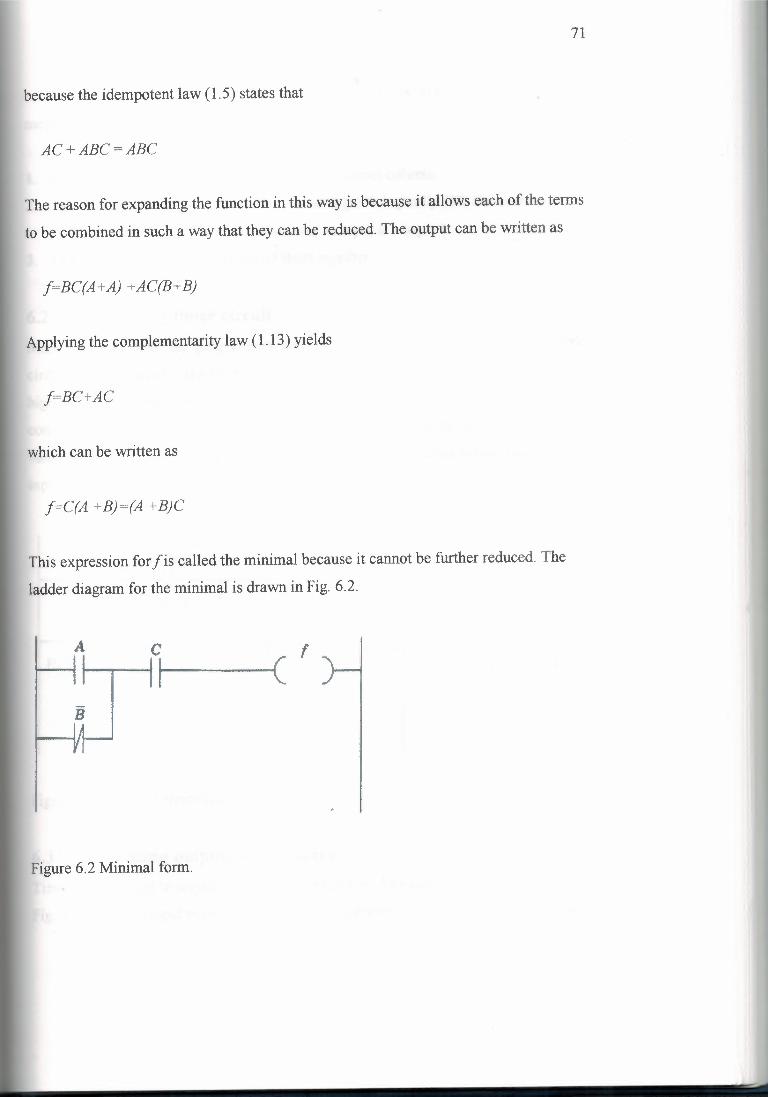
71
because the idempotent law (1.5) states that
AC+ABC=ABC
The reason for expanding the function in this way is because it allows each of the terms
to be combined in such a way that they can be reduced. The output can be written as
f=BC(A+A) +AC(B+B)
Applying the complementarity law (1.13) yields
f=BC+AC
which can be written as
f=C(A +B)=(A +B)C
This expression forf is called the minimal because it cannot be further reduced. The
ladder diagram for the minimal is drawn in Fig. 6.2.
A C l-.JI ' ıı C f
Figure 6.2 Minimal form.
72
An alternative approach to solving this problem would be to use the product-of-sums
method. This is applied using the following rules:
1. Pick out the rows that contain a logic O in the output column.
2. For each row that has an output equal to logic O logically OR the corresponding
inputs together using a negation whenever an input is a logic 1.
3. Take all the row products and AND them together.
6.2 An off-delay timer circuitMany PLCs provide the programmer with on-delay timers only. An off-delay timer
circuit can be created using an on-delay timer as shown in Fig. 6.3. The output Ql goes
high when the input Ii is set high and maintains itself high through the hold-in latch
contact. When input Ii is set low the timer resets the latch after the specified pre-set
value is reached. Consequently, the output is held for the specified pre-set time after the
input is taken low.
I1 TONI Qt
QıTiı:nerreset TONl
Hold~in contact Tl#5s
Figure 6.3 Off-delay timer circuit.
6.3 Controlling outputs using timersTimers can be used to sequence a set of output states. An example circuit is shown in
Fig. 6.4. When an input pulse is applied to Ii the outputs Ql, Q2 and Q3 are turned on
73
and off one after the other, as illustrated in the timing diagram. Each output is held on
for the specified pre-set time. The PLC scan ensures that the step-to-step sequencing of
outputs turning on and off is repeated
Overlap of the output on/off transitions can be achieved by using additional timers to
set the next output high before the previous output is taken low. An example ladder
circuit and timing diagram are shown in Fig. 6. 5.
rı TONI 12Ql
QlI -1TONl
T#5sTON3
TONl TON2 I2~ Q2l • I jI
ı IQ2
I
ITON2I I I
T#5sTON2 TONS 12
• Q3I ı ••
I IQ3
' -TON3I I
T#5s
End
74
u _.
- 5s ---... ..,._._ 5s -
qı r I I L
II
• •~5s----:
Figure 6.4 Sequencing with overlap
75
Ql
I IQl
-TONl. '
'f#5sII
~~6 I I
~TON2T-#4s
Q2I I
Q2I ~TON3II I
T#5s
TON4.T#4s
Q3
I IQ3
"TONS'.T#5s
.TONG.T#4s
Ladder diagram
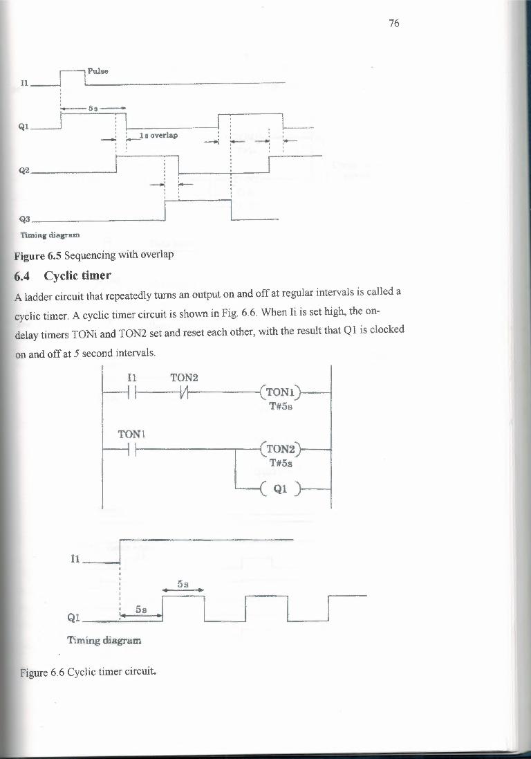
76
11 . nPulse----.•..:..--5s-
Ql I l I I---: ;.-ls overlap . '
-.( ' I:-- --: ~. ' '
Q2 ___,
.-. ':--
Q3~~~~~~~~~--.,
Timing diagram
Figure 6.5 Sequencing with overlap
6.4 Cyclic timer A ladder circuit that repeatedly turns an output on and off at regular intervals is called a
cyclic timer. A cyclic timer circuit is shown in Fig. 6.6. When Ii is set high, the on
delay timers TONi and TON2 set and reset each other, with the result that Ql is clocked
on and off at 5 second intervals.
Il TON2~ I vı -{TONI ) I
T#5s
TON1
I
u_---ı
Ql--~== .Timing diagram
Figure 6.6 Cyclic timer circuit.
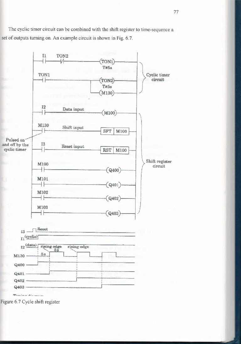
77
The cyclic timer circuit can be combined with the shift register to time-sequence a
set of outputs turning on. An example circuit is shown in Fig. 6.7.
TON2 (TONl---,vJ T#Ss
TONl
' tTON2T#5sMl30 ~· ----ı
Cyclic timercircuit
12 Data input (MlOO ı -ıI
M130Shift input SFT I MlOO
Pulsed Oiland off by thecyclic timer
13Re.setinput RST I MlOO
MlOO Shi~ registercircuit
t----------l Q400} I
M101
M102
Ml OSı-----~-----i Q403 I J
13___n~R=~=se~t----~~---~-----------rı(cyclic)!
ı2 (data) J rising edge ri_singedge• "'-. 5s ".,----,
Ml30 l 5s ! I I I !•
Q400Q401 ___.
Q402-----------~Q403--~~-~-----------....ı
Figure 6.7 Cycle shift register
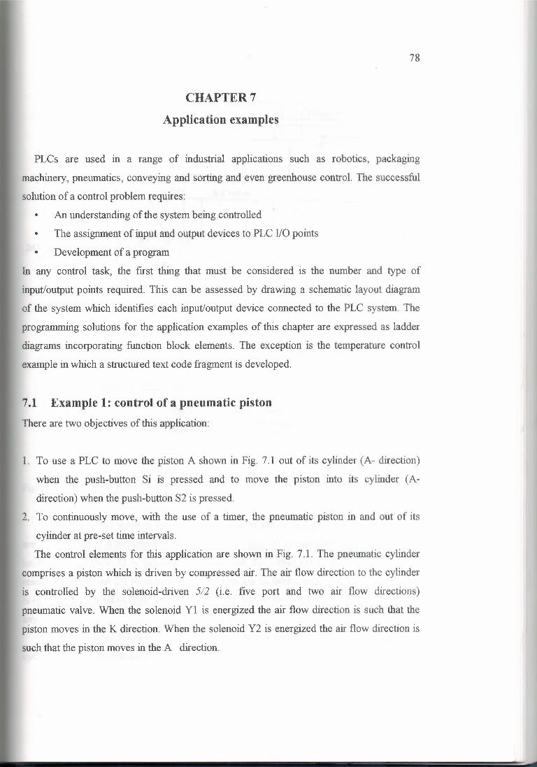
78
CHAPTER7
Application examples
PLCs are used in a range of industrial applications such as robotics, packaging
machinery, pneumatics, conveying and sorting and even greenhouse control. The successful
solution of a control problem requires:
• An understanding of the system being controlled
• The assignment of input and output devices to PLC I/O points
• Development of a program
In any control task, the first thing that must be considered is the number and type of
input/output points required. This can be assessed by drawing a schematic layout diagram
of the system which identifies each input/output device connected to the PLC system. The
programming solutions for the application examples of this chapter are expressed as ladder
diagrams incorporating function block elements. The exception is the temperature control
example in which a structured text code fragment is developed.
7.1 Example 1: control of a pneumatic piston
There are two objectives of this application:
1. To use a PLC to move the piston A shown in Fig. 7.1 out of its cylinder (A- direction)
when the push-button Si is pressed and to move the piston into its cylinder (A
direction) when the push-button S2 is pressed.
2. To continuously move, with the use of a timer, the pneumatic piston in and out of its
cylinder at pre-set time intervals.
The control elements for this application are shown in Fig. 7 .1. The pneumatic cylinder
comprises a piston which is driven by compressed air. The air flow direction to the cylinder
is controlled by the solenoid-driven 5/2 (i.e. five port and two air flow directions)
pneumatic valve. When the solenoid Yl is energized the air flow direction is such that the
piston moves in the K direction. When the solenoid Y2 is energized the air flow direction is
such that the piston moves in the A direction.
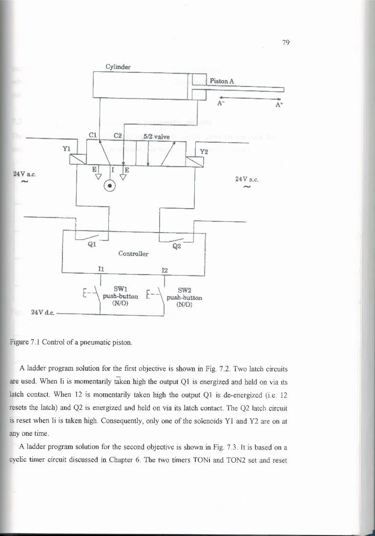
79
Cylinder
Pisten A
.512 valve
E24V a,c.24Va.c.-
Ql Q2Controller
I1 12
24V d.e, ---- ....•.------.........ı
swıpush-button
{N/0)E-- SW2
push-button(N/0)
Figure 7 .1 Control of a pneumatic piston.
A ladder program solution for the first objective is shown in Fig. 7.2. Two latch circuits
are used. When Ii is momentarily taken high the output Q 1 is energized and held on via its
latch contact. When 12 is momentarily taken high the output QI is de-energized (i.e. 12
resets the latch) and Q2 is energized and held on via its latch contact. The Q2 latch circuit
is reset when Ii is taken high. Consequently, only one of the solenoids YI and Y2 are on at
any one time.
A ladder program solution for the second objective is shown in Fig. 7 .3. It is based on a
cyclic timer circuit discussed in Chapter 6. The two timers TONi and TON2 set and reset
80
each other at 5 s intervals, with the result that Ql and Q2 are toggled (i.e. switched so that
when Ql is on Q2 is off and vice versa) every 5 s. Consequently, the piston moves in and
out of its cylinder every 5 s.
7.2 Example 2: sequencing three pneumatic pistons
The objective of this application is to use timers to operate three pistons such that the
sequence A-, A-, B-, W, C-, C is repeated. The three pneumatic pistons shown
~~ ~ (Q2
Q2
Figure 7.2 Circuit for controlling the pneumatic piston.
TON2 'TONI
ı.ı
T#5s TONl
I -{TON2 IT#5s
{Ql
TONI 'Q2
I .I
81
Figure 7 .3 cyclic timer circuit for controlling the piston .
in Fig. 7.4 are controlled using the three 512 directional control valves. Each solenoid has
to be held energized for 5 s to allow time for the piston to move. A ladder solution to this
problem is shown in Fig. 7 .5.
7.3 Example 3: counting and packaging
The objective of this application is to continuously divert components down one of two
chutes. Figure 7 .6 illustrates the application, the assignment of PLC input/output points
and a ladder program solution. The requirement is for ten components to be directed down
chute A and twenty components down chute B for packaging purposes.
o
Figure 7.4 Control of the pneumatic pistons .
.,...a
.§-=~..ı;ı00 .c
~ I~"ti>..,.
I I~w
82
83
l"\A Q5 Q6 I1 TONl 9~ ~~ ·~ .. .. ~Ql.,-,}
A*'1. ~Ql I TONl
T#5s
TON! TON2 CQ2J }p ~ A-w.- TON2
'f#5e ,ı
TON2 TO. N3 ( Q3'ı. }p ~ l ,~~ B'~ · - TO. N3 T#5s
TO. N3 TON4 C Q4J }
~ ~ B-Q4- TON4
T#5s
TON4 TONS • CQ5'ı }p ~ .~ ~Q5~ TON5
T#5s
TON5 TON6 CQ.· 6_J }.p ~ . ~~ TON6
T#5s
"End
Figure 7. 5 Circuit for sequencing the pistons.
A solenoid-drivenflap is used to direct components down either chute A or chute B.
When the solenoid is energized components are routed down path B. When the solenoid is
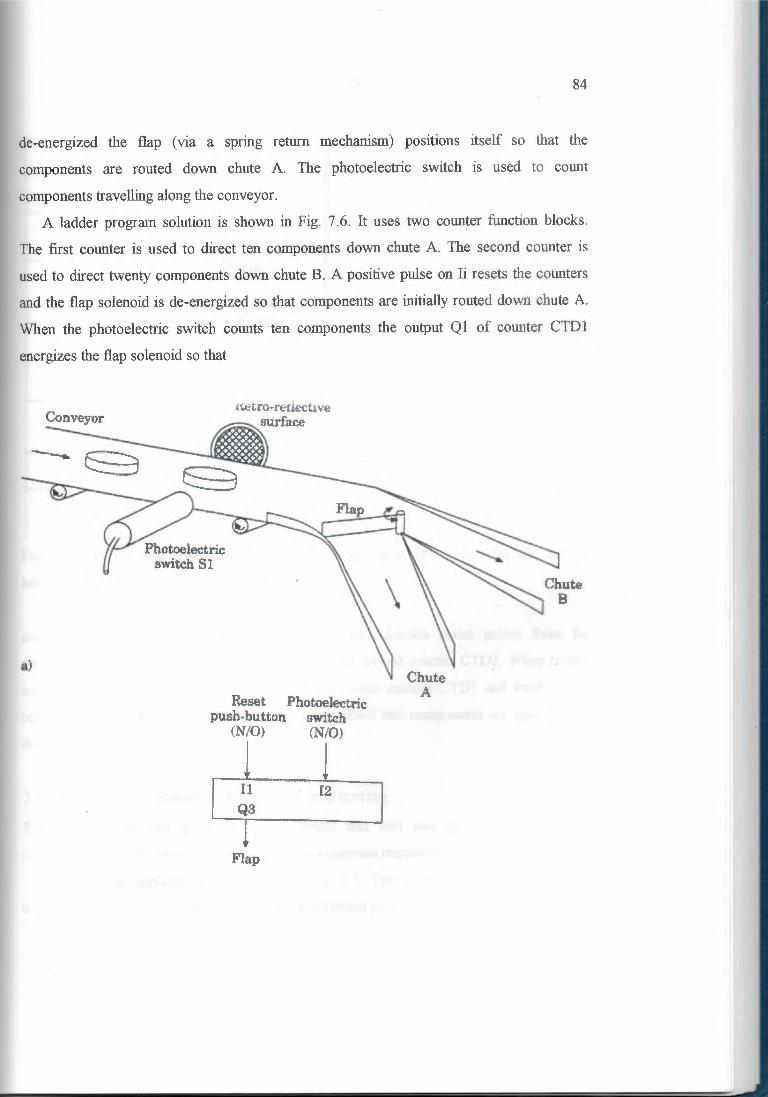
84
de-energized the flap (via a spring return mechanism) positions itself so that the
components are routed down chute A The photoelectric switch is used to count
components travelling along the conveyor.
A ladder program solution is shown in Fig. 7 .6. It uses two counter function blocks.
The first counter is used to direct ten components down chute A The second counter is
used to direct twenty components down chute B. A positive pulse on Ii resets the counters
and the flap solenoid is de-energized so that components are initially routed down chute A
When the photoelectric switch counts ten components the output Ql of counter CTDl
energizes the flap solenoid so that
Reset Phot.oelectricpush-button switch
(N/0) (N/0)
ıı raQa
Flap
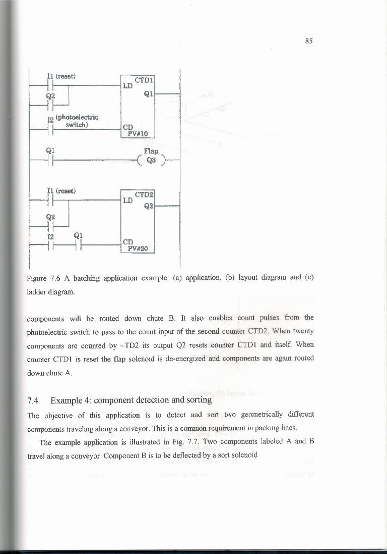
85
il (reset) I . CTD1~I LD Qll I
ı2 (photoelectricl---1 I switeh} I CD
PV#lO
Ql Flap~I C Qs
u (reset} I CTD2LD
Q2II
Q2
~~ Ql
1cııv-#20t II
Figure 7.6 A batching application example: (a) application, (b) layout diagram and (c)
ladder diagram.
components will be routed down chute B. It also enables count pulses from the
photoelectric switch to pass to the count input of the second counter CTD2. When twenty
components are counted by - TD2 its output Q2 resets counter CID 1 and itself. When
counter CTD 1 is reset the flap solenoid is de-energized and components are again routed
down chute A
7.4 Example 4: component detection and sortingThe objective of this application is to detect and sort two geometrically different
components traveling along a conveyor. This is a common requirement in packing lines.
The example application is illustrated in Fig. 7.7. Two components labeled A and B
travel along a conveyor. Component B is to be deflected by a sort solenoid
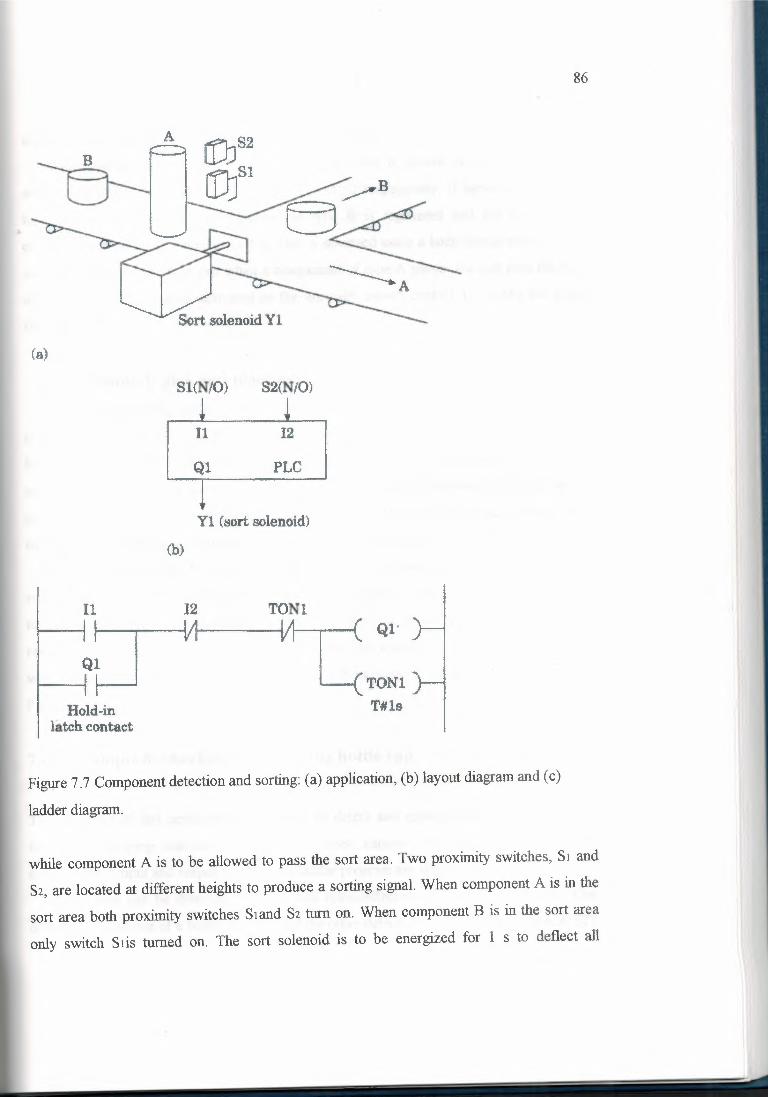
86
(a)
Sl(N/0) S2(N/0}
11 12
Ql PLC
Yl (sort solenoid)
{b)
r-c Qı·
LcTONlHold~in
latch contactTIils
Figure7.7 Componentdetectionand sorting:(a) application,(b) layout diagramand (c)
ladder diagram.
while componentA is to be allowed to pass the sort area. Two proximityswitches, Sı and
S2, are located at differentheights to produce a sorting signal.When componentA is in the
sort area both proximityswitches Sıand S2 turn on. When componentB is in the sort area
only switch Sıis turned on. The sort solenoid is to be energized for 1 s to deflect all
87
components of type B down a different conveyor feed path.
A PLC layout diagram and ladder program solution is shown in Fig. 7. 7. Proximity
switches Sıand S2 are connected to inputs Ii and 12 respectively. If input Ii (i.e. Sı)goes
high but not 12 (i.e. S2) a component of type B is registered and the sort solenoid
connected to coil Qıis activated for I s. This is achieved using a latch circuit which is reset
using the timer TONı Note that when a component of type A passes the sort area the solen
id is prevented from being activated as the normally closed contact 12 breaks the power
flow path to Qı .
7.5 Example 5: pick and place unitThe objective of this applicationis to show how position switchescan be used to control
the movementof an axis of a pick and place unit. The pick and place unit shown in Fig. 7 .8
has one rotary (O) and two linear (X and Z) degrees of freedom. The motions are on/off in
nature, being actuated by pneumaticpistons. For example, the X motion is in either the X~
position or the X position. The gripper can also be pneumaticallyoperated, being either
open or shut.Actuatingappropriatesolenoidscontrolsallmotions.Position switches can be mounted on the unit so that they turn on when a particular
motion has occurred. For example, consider two position switches Sı and 52 mounted so
that they register the fully extended'X- position (i.e. Sı is on and S2 is off) and the fully
retracted X position (i.e. Sı is off and S2 is on). An example ladder program fragment
which uses these signals to sequence the X~ and X movementsback and forth is shown in
Fig. 7.8.
7.6 Example 6: checking for a missing bottle cap
The objective of this application example is to detect and reject bottles emerging from a
filling and capping machine that have not been capped. An application sketch, the
assignmentof input and outputpoints and a ladderprogramare shownin Fig. 7.9.
Bottle caps can be detected by using two retro-reflective photoelectric switches. One
detects the presence of a bottle (i.e. SI) and the other detects the presence of a cap (i.e. S2).
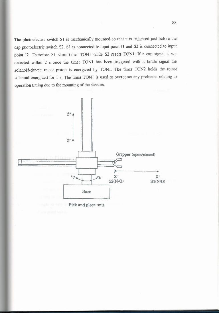
88
The photoelectric switch SI is mechanically mounted so that it is triggered just before the
cap photoelectric switch S2. SI is connected to input point I1 and S2 is connected to input
point 12. Therefore SI starts timer TONI while S2 resets TONI . If a cap signal is not
detected within 2 s once the timer TONI has been triggered with a bottle signal the
solenoid-driven reject piston is energized by TONI. The timer TON2 holds the reject
solenoid energized for I s. The timer TONI is used to overcome any problems relating to
operationtimingdue to the mountingof the sensors.
z+"'
z-,
ı1 I Gripper (open/closed}
II'=
·~:•eile ~
x- x+S.2(N/O) Sl(N/0)
Base
Pick and place unit
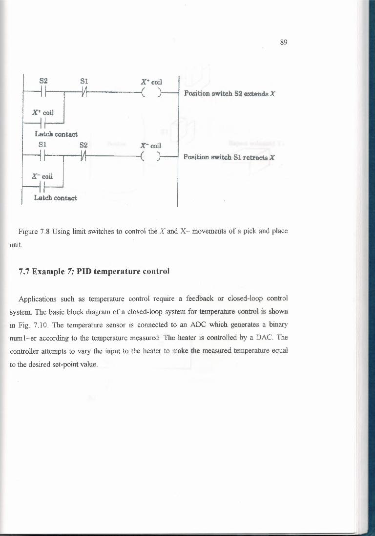
89
S2 sı x+ coil
- Position switch S2 extendsX
x• coil
Latch eontaetsı sa x-coil
Position switch S1 retracts X
x-coil
Latch contact
Figure 7.8 Using limit switches to control the X and X- movements of a pick and place
unit.
7.7 Example 7: PID temperature control
Applications such as temperature control require a feedback or closed-loop control
system. The basic block diagram of a closed-loop system for temperature control is shown
in Fig. 7.10. The temperature sensor is connected to an ADC which generates a binary
numI+er according to the temperature measured. The heater is controlled by a DAC. The
controller attempts to vary the input to the heater to make the measured temperature equal
to the desired set-point value.
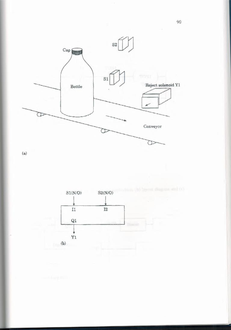
90
s2(VJ
Bottlesı[f}J
Conveyor
(a)
Sl(N/0) S2(N/O)
I1
Ql
12
Y1(b)
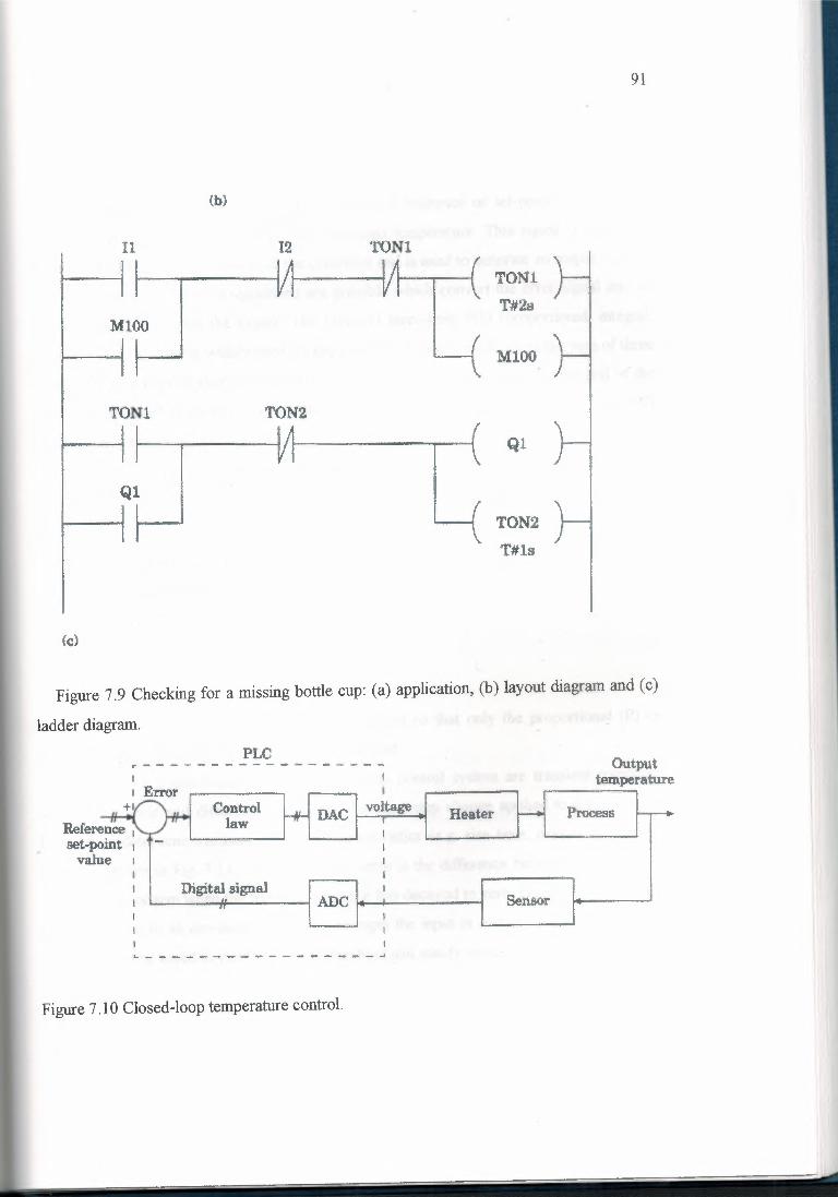
91
{b}
12 TON1( TONl
HI ı1 I A
T#2sII
I I M100
MlOOJ I I
\
TONl TON2l
QlI A
ı \I V Ir: J
ı f TON2
QlI I I
T#1s
(c)
Figure 7.9 Checking for a missing bottle cup: (a) application, (b) layout diagram and (c)
ladder diagram.
PLC Outputtemperature
r-----------------~Contröl
law Heater Process
ı.......---ıı------ıADC I• ı IDigital signal
I~-----------------~Figure 7 .1 O Closed-loop temperature control.
92
The comparator detects the difference between a reference or set-point value and the
output of the ADC which represents the measured temperature. This signal is called the
error signal.The error signalis fed to the controllerand is used to generatean output signal.Various types of control algorithmsare possible which convert the error signal into an
output signal for driving the heater. The classical three-term PID (proportional, integral,
derivative)control law is widely used. In this case the output is made up of the sum of threeterms. The first is proportional to the error, the second is proportionalto the integral of the
error and the third is proportional to the derivative or rate of change of error. The PID
controlaction equationcan be writtenas
wherex = controlleroutputKP
K; = proportionalgain
e = error
T, = integraltime
Td = derivativetimeOf course, it is possible to simplify the algorithm so that only the proportional (P) or
proportionalplus integral(Pl) terms are implemented.The important specifications for a closed-loop control system are transient response,
steady state error and disturbance rejection. An input step change applied to a system canbe used to determine transient response characteristics (e.g. rise time, overshoot, settling
time), as shown in Fig. 7 .11. The steady state error is the differencebetween the input andoutput of the systemwhen the transient response has decayed to zero. Disturbancerejection
is the response to an unwanted signal that corrupts the input or output of a process. A PID
controllercan be tuned to yieldminimumovershootand steady state error.
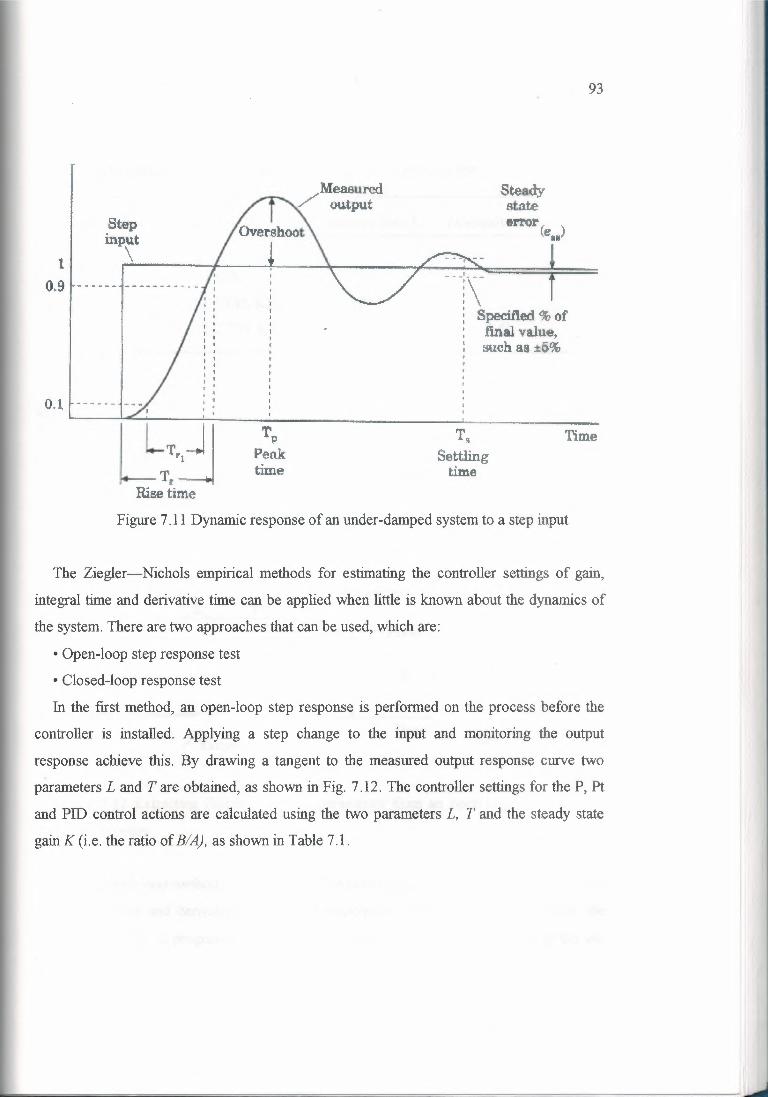
93
10.9
Meaaured/ output
Steadystateerror (e )
811Stepinput
\---r\
: Specified % of' fin.al value.
such as±5%
0.1
~T:~Rise time
Figure 7 .11 Dynamic response of an under-damped system to a step input
r,Settling
time
Time
The Ziegler-Nichols empirical methods for estimating the controller settings of gain,
integral time and derivative time can be applied when little is known about the dynamics of
the system. There are two approaches that can be used, which are:
• Open-loop step response test
• Closed-loop response test
In the first method, an open-loop step response is performed on the process before the
controller is installed. Applying a step change to the input and monitoring the output
response achieve this. By drawing a tangent to the measured output response curve two
parameters L and Tare obtained, as shown in Fig. 7.12. The controller settings for the P, Pt
and PID control actions are calculated using the two parameters L, T and the steady state
gain K (i.e. the ratio of BIA), as shown in Table 7.1.
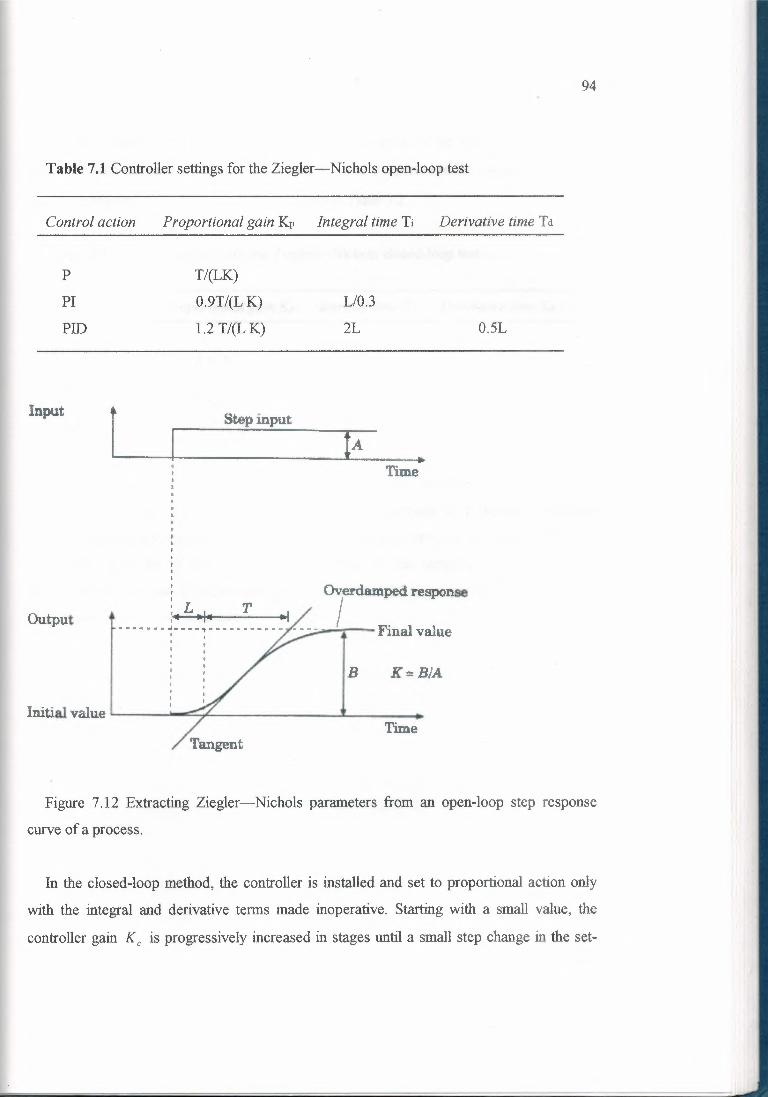
94
Table 7.1 Controller settings for the Ziegler-Nichols open-loop test
Control action Proportional gain Ks Integral time Ti Derivative time Ta
p
PI
PIO
T/(LK)
0.9T/(LK)
1.2 T/(L K)
L/0.3
2L O.SL
Input
tStep input
•'lime
OutputT
Overdaınped response
L Final value
B K=BIA
Time
Figure 7.12 Extracting Ziegler-Nichols parameters from an open-loop step response
curve of a process.
In the closed-loop method, the controller is installed and set to proportional action only
with the integral and derivative terms made inoperative. Starting with a small value, the
controller gain Kc is progressively increased in stages until a small step change in the set-
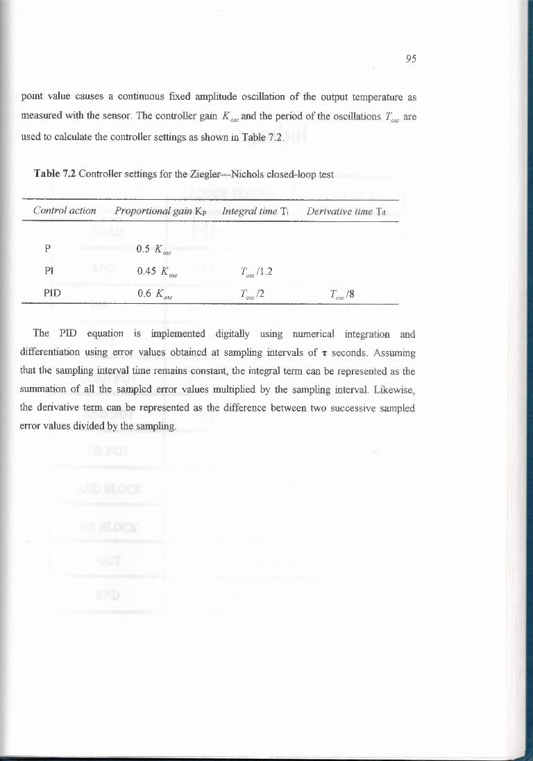
95
point value causes a continuous fixed amplitude oscillation of the output temperature as
measured with the sensor. The controller gain K osc and the period of the oscillations T0sc are
used to calculate the controller settings as shown in Table 7 .2.
Table 7.2 Controller settings for the Ziegler-Nichols closed-loop test
Control action Proportional gain Kp Integral time Ti Derivative time Ta
p 0.5 Kase
PI 0.45 Kosc Tosc/1.2
PID 0.6 K0,c Tosc/2 Tosc/8
The PID equation is implemented digitally using numerical integration and
differentiation using error values obtained at sampling intervals of T seconds. Assuming
that the sampling interval time remains constant, the integral term can be represented as the
summation of all the sampled error values multiplied by the sampling interval. Likewise,
the derivative term can be represented as the difference between two successive sampled
error values divided by the sampling.
96
Table of Symbol
INSTRUCTION LADDER SEMBOL SIMATICS7
LOAD ~ı- LD
AND -it- A
OR Li t-.t oNOT / NOT
LOADNOI l-tıt- LDN
AND NOT -ilt- AN
ORNOt 41-1 ON
AND BLOCK ALD
OR BLOCK OLD
OUT -o-; -<>ı -END -(END)- MEND
PROGRAM TITLE COMMENTS
Press Fl for help and example program
Network 1 CHOOSER BANDS
WHEN CONTACTS IO.O NORMALY OPEN CHANGE POSITION THE OUTPUT OFQO. O WORK
IO.O T37~,, t·) QO.O~
Network 2 WHEN THE QO.O STOP
IF IO.O NORMALY CLOSED CONTACT AND QO.O NORMALY OPENCONTACTS ARE CLOSED AND THEN T37 WILL WORK .WHEN THE T37 WORK,CONTACTS's POSITION WILL CHANGE AFTER 30 SECOND.
IO.O QO.O
I I I I ]IN IDNI+300 c,PT.;.._-...J.
T37
Network 3 WHEN THE QO.l START.
WHEN THE CONTACT POSITION OF Q O.O OUTPUT CHANGET38 WILL WORK .WHEN THE T38 WORK,CONTACTS WILL CHANGE POSITIONAFTER 10 SECONDS.
QO.O
IT38
1
97
2
Network 4 WHEN THE WASHING START
98WHEN NORMALLY OPEN CONTACTS OF T38 CLOSED QO.l OUTPUT WILL WORK.AND QO.l OUTPUTLOCK ITSELF WITH QO.l NORMALY OPEN CONTACTS.
T38 T39"r': ı t.QO.l~
Network 5 WHEN THE JET OF WATER WORKS
WHEN QO.l OUTPUT STARTS TO WORK,QO.l OUTPUT CONTACT WILL CHANGE POSITIONAND THEN Q0.2 START WORK.
QO.l Q0.2
I C )
Network 6 WHEN THE WASHES STOP
IF Q0.0 NORMALY CLOSED CONTACT AND QO.l NORMALY OPENCONTACTS ARE CLOSED ,THEN T39 WILL WORK .WHEN THE T37 WORK,CONTACTS's POSITION WILL CHANGE AFTER 30 SECOND.
QO.O Q0.1 T39
I I I I JIN "'"I-sco ._.P.;...T ----'·
Network 7 DISINFECTOR START WAITING FOR WORK
IF QO.lNORMALY OPEN CONTACT CLOSED, T40 START TO WORK.THENT40 WILL CHANGE CONTACTS POSITION AFTER 30 SECONDS.
Q0.1
IT40
Network 8 DISINFECT IS WORK
99T40 NORMA.LY OPEN CONTACT CLOSED Q0.3 OUTPUT WORK.LOCKED BY THE Q 0.3NORMA.LY OPEN CONTACT.
T40 TT;ılQ0.3~
Network 9 JET OF DISINFECT LIQUID WORK
WORK THE SAME TIME Q0.3 NORMA.LY OPEN CONTACT WHEN THE CLOSED Q0.4 WORK.
Q0.3 Q0.4
I C )
Network 10 WHEN THE DISINFECT STOP
IF QO.l NORMA.LY CLOSE CONTACTS AND Q0.4 NORMA.LY OPEN CONTACT CLOSEDT41 WILL START WORK.WHEN THE T41 WORK, IT CHANGE THE CONTACTAFTER 30 SECONDS.
QO.l Q0.4 T41
I I I I l!N roNI+300 ı.;.. P.:.T---'·
Network 11 DIMENSION START WAITING FOR WORK
WHEN THE Q0.4 NORMA.LY OPEN CONTACT CLOSED T42 WORK.WHEN THET42 TIMER CHANGE THE CHANGE THE POSITIONS OFTHE CONTACTS AFTER 10 SECONDS.
Q0.4
IT42
3
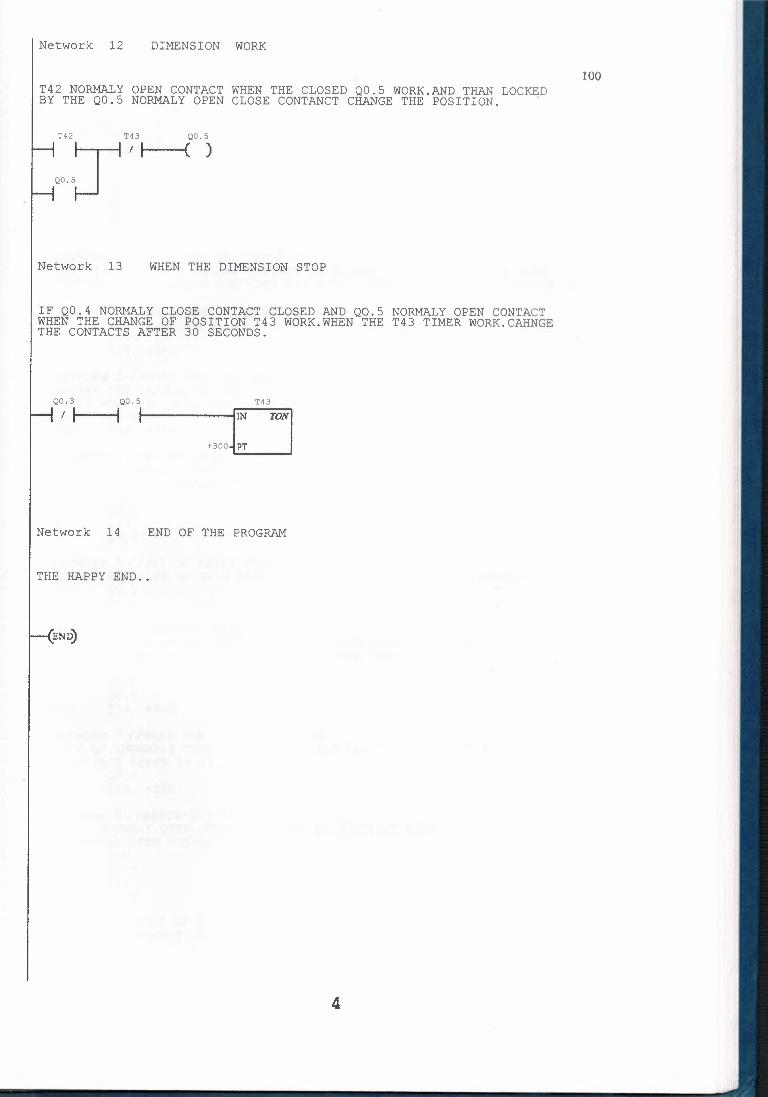
100
Network 12 DIMENSION WORK
T42 NORMALY OPEN CONTACT WHEN THE CLOSED Q0.5 WORK.AND THAN LOCKEDBY THE Q0.5 NORMALY OPEN CLOSE CONTANCT CHANGE THE POSITION.
T42 T43
1 11 t.Q0.5
Network 13 WHEN THE DIMENSION STOP
IF Q0.4 NORMALY CLOSE CONTACT CLOSED AND Q0.5 NORMALY OPEN CONTACTWHEN THE CHANGE OF POSITION T43 WORK.WHEN THE T43 TIMER WORK.CAHNGETHE CONTACTS AFTER 30 SECONDS.
Q0.3 Q0.5
I I I I i!N TONI +3üü~PT.__ _
T43
Network 14 END OF THE PROGRAM
THE HAPPY END ..
END)
4
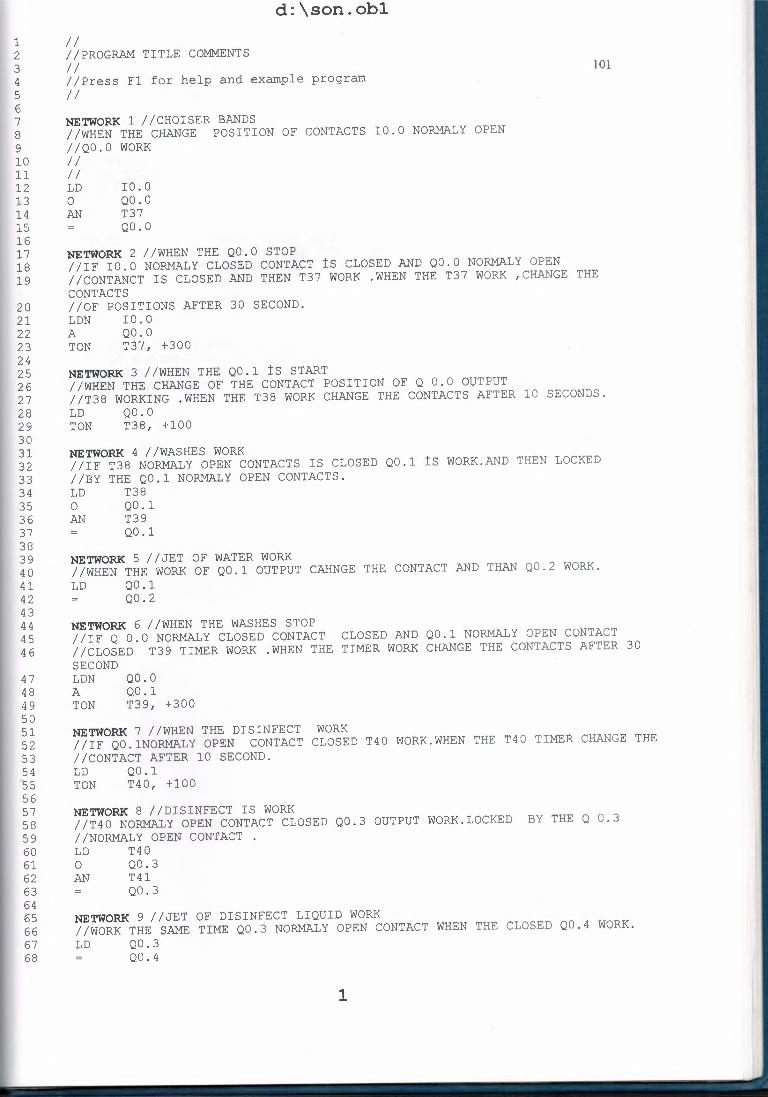
12345678910111213141516171819
202122232425262728293031323334353637383940414243444546
47484950515253545556575859606162636465666768
d:\son.obl
II //PROGRAM TITLE COMMENTSII //Press Fl for help and example programII
101
NETWORK 1 / /CHOISER BANDS//WHEN THE CHANGE POSITION OF CONTACTS IO.O NORMALY OPEN//QO.O WORKII II LDoAN
IO.OQO.OT37QO.O
NETWORK 2 //WHEN THE QO.O STOP//IF IO.O NORMALY CLOSED CONTACT !S CLOSED AND QO.O NORMALY OPEN//CONTANCT IS CLOSED AND THEN T37 WORK .WHEN THE T37 WORK ,CHANGE THECONTACTS//OF POSITIONS AFTER 30 SECOND.LDN IO.OA QO.OTON T37, +300
NETWORK 3 //WHEN THE QO.l !S START//WHEN THE CHANGE OF THE CONTACT POSITION OF Q O.O OUTPUT//T38 WORKING .WHEN THE T38 WORK CHANGE THE CONTACTS AFTER 10 SECONDS.LD QO.OTON T38, +100
NETWORK 4 / /WASHES WORK//IF T38 NORMALY OPEN CONTACTS IS CLOSED QO.l !S WORK.AND THEN LOCKED//BY THE QO.l NORMALY OPEN CONTACTS.LD T38O QO.lAN T39
QO.l
NETWORK 5 // JET OF WATER WORK//WHEN THE WORK OF QO.l OUTPUT CAHNGE THE CONTACT AND THAN Q0.2 WORK.LD QO.l
Q0.2
NETWORK 6 / /WHEN THE WASHES STOP//IF Q O.O NORMALY CLOSED CONTACT CLOSED AND QO.l NORMALY OPEN CONTACT//CLOSED T39 TIMER WORK .WHEN THE TIMER WORK CHANGE THE CONTACTS AFTER 30SECONDLDN QO.OA QO.lTON T39, +300
NETWORK 7 //WHEN THE DISINFECT WORK//IF QO.lNORMALY OPEN CONTACT CLOSED T40 WORK.WHEN THE T40 TIMER CHANGE THE//CONTACT AFTER 10 SECOND.LD QO.lTON T40, +100
NETWORK 8 //DISINFECT IS WORK//T40 NORMALY OPEN CONTACT CLOSED Q0.3 OUTPUT WORK.LOCKED BY THE Q 0.3//NORMALY OPEN CONTACT.LD T40O Q0.3AN T41
Q0.3
NETWORK 9 //JET OF DISINFECT LIQUID WORK//WORK THE SAME TIME Q0.3 NORMALY OPEN CONTACT WHEN THE CLOSED Q0.4 WORK.LD Q0.3
Q0.4
1

69707172737475767778798081828384858687888990919293949596979899100101102
d:\son.obl
NETWORK 10 //WHEN THE DISINFECT STOP//IF Q0.1 NORMALY CLOSE CONTACTS CLOSED AND Q0.4 NORMALY OPEN CONTAC10i //WHEN THE CLOSED T41 WORK.WHEN THE T41 WORK CHANGE THE CONTACT//AFTER 30 SECONDS.LDN Q0.1A QO. 4TON T41, +300
NETWORK 11 //WHEN THE DIMENSION WORK//WHEN THE Q0.4 NORMALY OPEN CONTACT CLOSED T42 WORK.WHEN THE //T42 TIMER CHANGE THE CHANGE THE POSITIONS OFTHE CONTACTS AFTER 10 SECONDS.LD Q0.4TON T42, +100
NETWORK 12 //T42 NORMALY//BY THE Q0.5LD T42O Q0.5AN T43
Q0.5
//DIMENSION IS WORKOPEN CONTACT WHEN THE CLOSED Q0.5 WORK.AND THAN LOCKEDNORMALY OPEN CLOSE CONTANCT CHANGE THE POSITION.
NETWORK 13 //WHEN THE DIMENSION STOP//IF Q0.4 NORMALY CLOSE CONTACT CLOSED AND Q0.5 NORMALY OPEN CONTACT//WHEN THE CHANGE OF POSITION T43 WORK.WHEN THE T43 TIMER WORK.CAHNGE//THE CONTACTS AFTER 30 SECONDS.LDN Q0.3A Q0.5TON T43, +300
NETWORK 14 //END OF THE PROGRAM//THE HAPPY END ..MEND
2
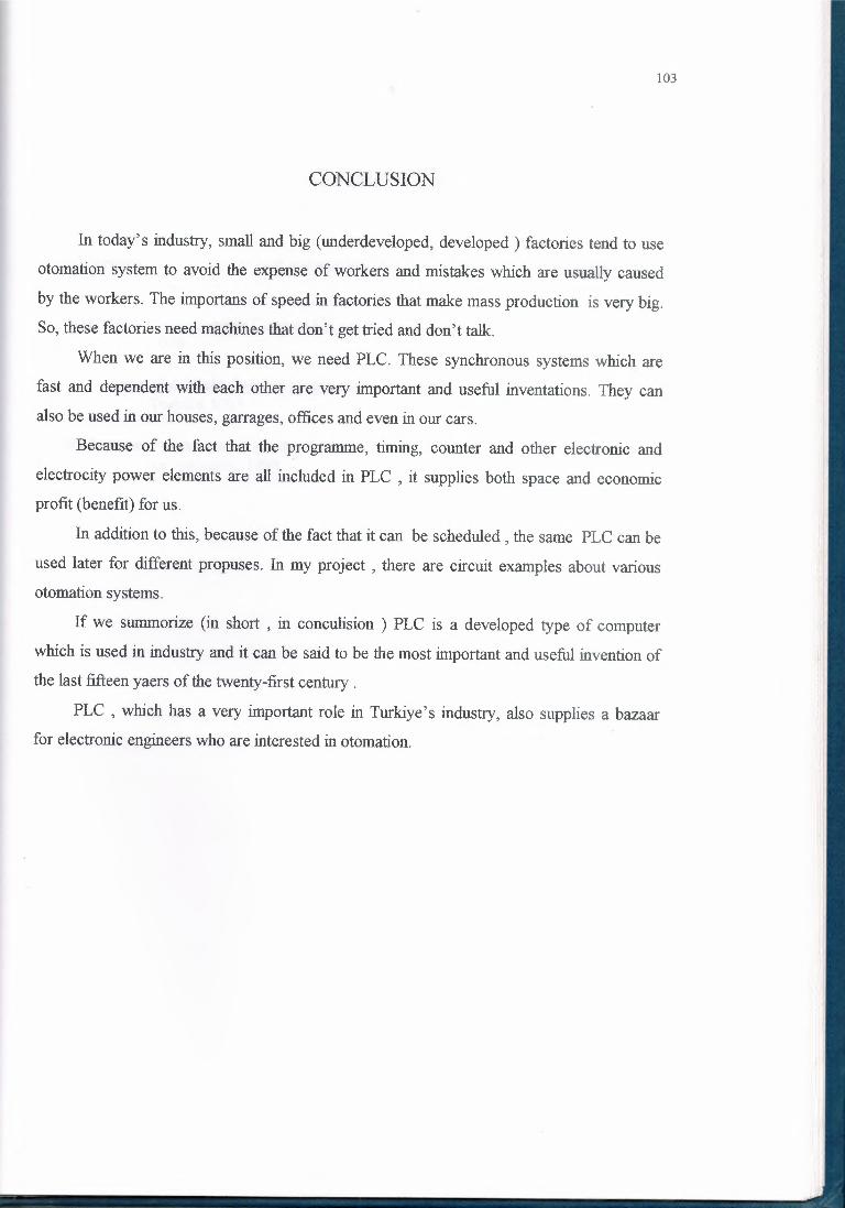
103
CONCLUSION
In today's industry, small and big (underdeveloped, developed) factories tend to use
otomation system to avoid the expense of workers and mistakes which are usually caused
by the workers. The importans of speed in factories that make mass production is very big.
So, these factories need machines that don't get tried and don't talk.
When we are in this position, we need PLC. These synchronous systems which are
fast and dependent with each other are very important and useful inventations. They can
also be used in our houses, garrages, offices and even in our cars.
Because of the fact that the programme, timing, counter and other electronic and
electrocity power elements are all included in PLC , it supplies both space and economic
profit (benefit) for us.
In addition to this, because of the fact that it can be scheduled , the same PLC can be
used later for different propuses. In my project , there are circuit examples about various
otomation systems.
If we summarize (in short , in conculision ) PLC is a developed type of computer
which is used in industry and it can be said to be the most important and useful invention of
the last fifteen yaers of the twenty-first century .
PLC , which has a very important role in Turkiye' s industry, also supplies a bazaar
for electronic engineers who are interested in otomation.
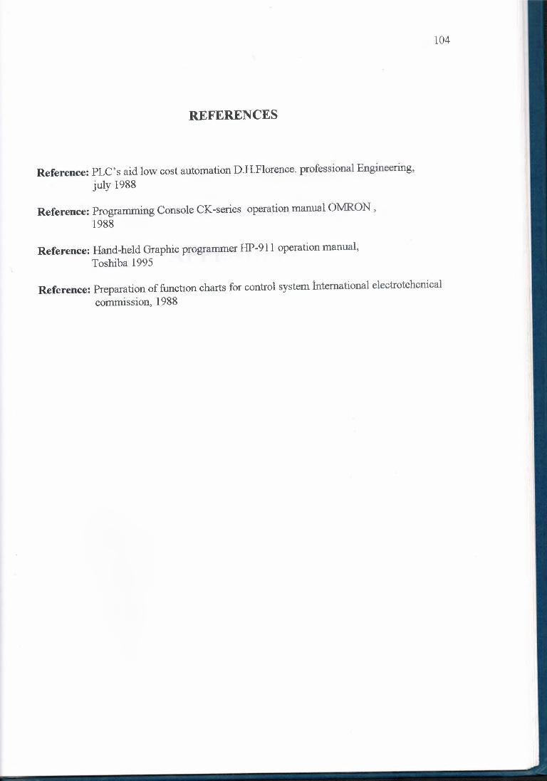
104
REFERENCES
Reference: PLC's aid low cost automation D.H.Florence. professional Engineering,july 1988
Reference: Programming Console CK-series operation manual OMRON,1988
Reference: Hand-held Graphic programmer HP-911 operation manual,Toshiba 1995
Reference: Preparation of functıon charts for control system İnternational electrotehcnicalcommission, 1988

106
Normally Open Contact
Symbol:
Operands:n (bit): I, Q, M, SM, T,
C,V,S
POS 210:10.0-10.3M0.0-M?.7SM0.0- SM1.7
Description of operation:
The Normally Open Contact is closed when the scanned bit value stored at address n is equal to 1.Power flows through a normally open contact when closed (activated).
Used in series, a normally open contact is linked to the next LAD element by AND logic. Used inparallel, it is linked by OR logic.
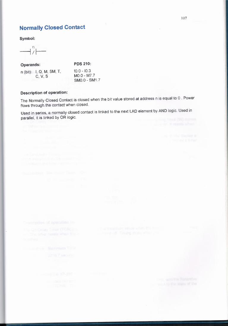
107
Normally Closed Contact
Symbol:
n--lı~Operands:
n (bit): I, Q, M, SM, T,C,V, S
POS 210:
10.0 -10.3MO.O- M7.7SMO.O - SM1 .7
Description of operation:
The Normally Closed Contact is closed when the bit value stored at address n is equal to O . Powerflows through the contact when closed.Used in series, a normally closed contact is linked to the next LAD element by AND logic. Used inparallel, it is linked by OR logic.
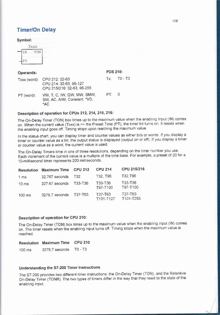
108
Timer/On Delay
Symbol:Txxx
~-h._JOperands:Txxx (word): CPU 212: 32-63
CPU 214: 32-63, 96-127CPU 215/216: 32-63, 96-255
PT (word): VW, T, C, IW, QW, MW, SMW,SW, AC, AIW, Constant, "'VD,*AC
PDS 210:
Tx: TO -T3
PT: O
Description of operation for CPUs 212, 214, 215, 216:The On-Delay Timer (TON) box times up to the maximum value when the enabling Input (IN) comeson. When the current value (Txxx) is>= the Preset Time (PT), the timer bit turns on. It resets whenthe enabling input goes off. Timing stops upon reaching the maximumvalue.
In the status chart, you can display timer and counter values as either bits or words. If you display atimer or counter value as a bit, the output status is displayed (output on or off). If you display a timeror counter value as a word, the current value is used.The On-Delay Timers time in one of three resolutions, depending on the timer number you use.Each increment of the current value is a multiple of the time base. For example, a preset of 20 for a1 O-millisecondtimer represents 200 milliseconds.
Resolution Maximum Time CPU 212 CPU 214 CPU 215/216
1 ms 32.767 seconds T32 T32, T96 T32,T96
10 ms 327.67 seconds T33-T36 T33-T36 T33-T36T97-T100 T97-T100
100 ms 3276.7 seconds T37-T63 T37-T63 T37-T63T101-T127 T101-T255
Description of operation for CPU 210:The On-Delay Timer (TON) box times up to the maximum value when the enabling input (IN) comeson. The timer resets when the enabling input turns off. Timing stops when the maximum value isreached.
Resolution Maximum Time CPU 210
100 ms 3276.7 seconds TO - T3
Understanding the 57-200 Timer InstructionsThe S7-200 provides two different timer instructions: the On-Delay Timer (TON), and the RetentiveOn-Delay Timer (TONR). The two types of timers differ in the way that they react to the state of theenabling input.

109• Both timers count up while the enabling input is on.
• Neither timer counts while the enabling input is off.• When the enabling input is off, a TON timer automatically resets the time value, while a TONR
timer does not reset, but instead retains the last count (or time) value. When a TONR timer isenabled again, new time value adds to the previous time value.
Therefore, the TON timer is best used when you are timing a single interval. The TONR timer isappropriate when you need to measure the accumulated time for a number of timed intervals.
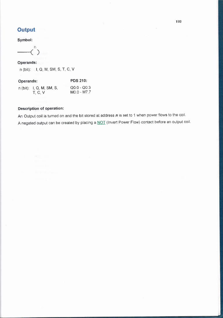
100
Output
Symbol:
n-c )Operands:
n (bit): I, Q, M, SM, S, T, C, V
Operands:n (bit): I, Q, M, SM, S,
T, C,V
POS 210:Q0.0-Q0.3MO.O - M7.7
Description of operation:
An Output coil is turned on and the bit stored at address n is set to 1 when power flows to the coil.
A negated output can be created by placing a NOT (Invert Power Flow) contact before an output coil.
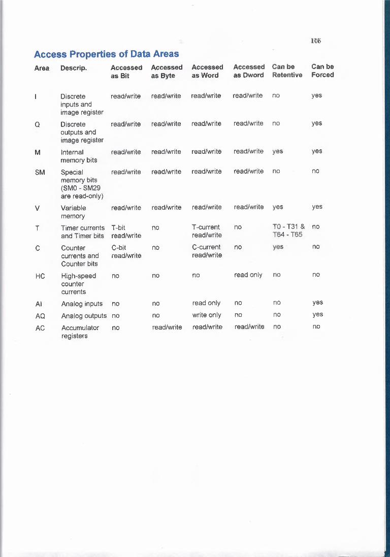
IDoAccess Properties of Data AreasArea Oescrip. Accessed Accessed Accessed Accessed Can be Can be
as Bit as Byte as Word as Dword Retentive Forced
Discrete read/write read/write read/write read/write no yesinputs andimage register
Q Discrete read/write read/write read/write read/write no yesoutputs andimage register
M Internal read/write read/write read/write read/write yes yesmemory bits
SM Special read/write read/write read/write read/write no nomemory bits(SMO-SM29are read-only)
V Variable read/write read/write read/write read/write yes yesmemory
T Timer currents T-bit no T-current no TO- T31 & noand Timer bits read/write read/write T64 -T65
C Counter C-bit no C-current no yes nocurrents and read/write read/writeCounter bits
HC High-speed no no no read only no nocountercurrents
Al Analog inputs no no read only no no yes
AQ Analog outputs no no write only no no yes
AC Accumulator no read/write read/write read/write no noregisters