JFET AND MOSFET - BITS Pilani
21
BITS Pilani Dubai Campus JFET AND MOSFET Dr Jagadish Nayak
Transcript of JFET AND MOSFET - BITS Pilani

BITS Pilani Dubai Campus
JFET AND MOSFET
Dr Jagadish Nayak

BITS Pilani Dubai Campus
Junction Field Effect Transistors & Metal Oxide Semiconductor Field Effect Transistors
BITS Pilani, Dubai Campus
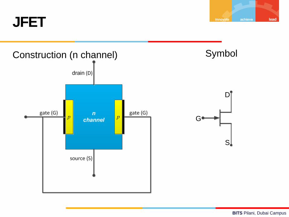
Construction (n channel)
JFET
S
G
D
Symbol
BITS Pilani, Dubai Campus
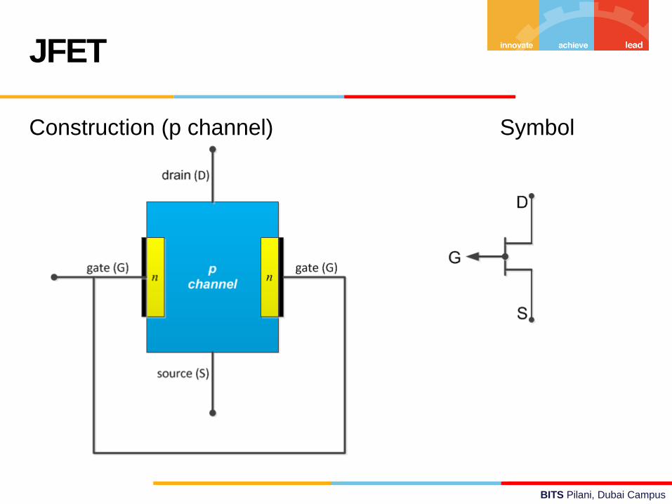
Construction (p channel) Symbol
JFET
BITS Pilani, Dubai Campus
JFET
BITS Pilani, Dubai Campus
JFET
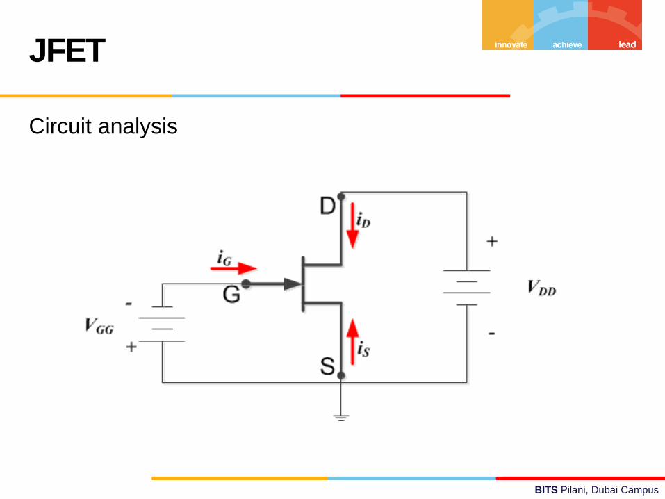
Circuit analysis

BITS Pilani, Dubai Campus
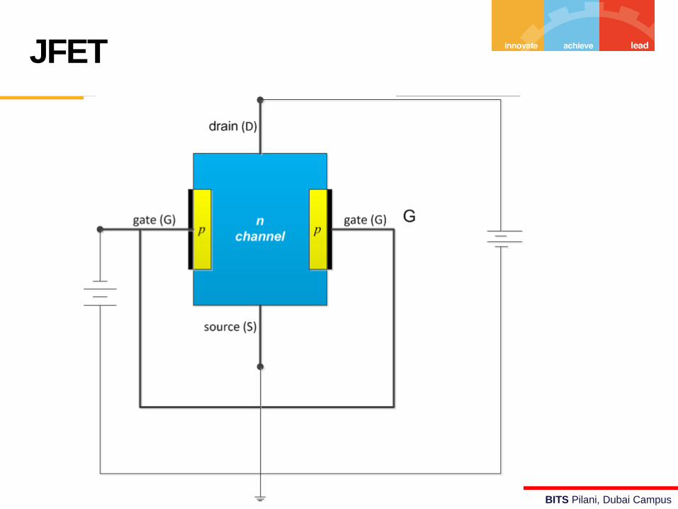
When VDD = VGG=0, two junctions
with associated depletion region
is shown
JFET
BITS Pilani, Dubai Campus
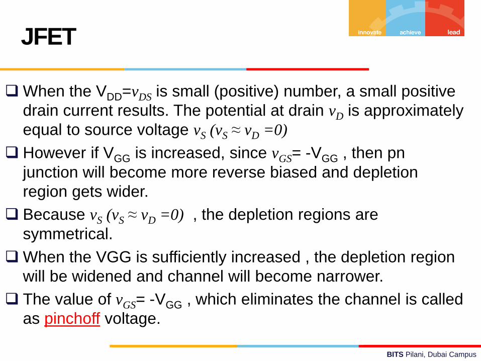
When the VDD=vDS is small (positive) number, a small positive
drain current results. The potential at drain vD is approximately
equal to source voltage vS (vS ≈ vD =0)
However if VGG is increased, since vGS= -VGG , then pn
junction will become more reverse biased and depletion
region gets wider.
Because vS (vS ≈ vD =0) , the depletion regions are
symmetrical.
When the VGG is sufficiently increased , the depletion region
will be widened and channel will become narrower.
The value of vGS= -VGG , which eliminates the channel is called
as pinchoff voltage.
JFET
BITS Pilani, Dubai Campus
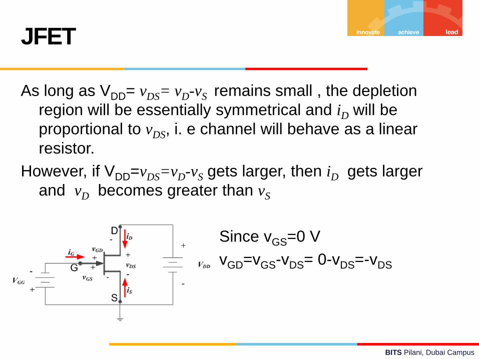
As long as VDD= vDS= vD-vS remains small , the depletion
region will be essentially symmetrical and iD will be
proportional to vDS, i. e channel will behave as a linear
resistor.
However, if VDD=vDS=vD-vS gets larger, then iD gets larger
and vD becomes greater than vS
Since vGS=0 V
vGD=vGS-vDS= 0-vDS=-vDS
JFET
BITS Pilani, Dubai Campus
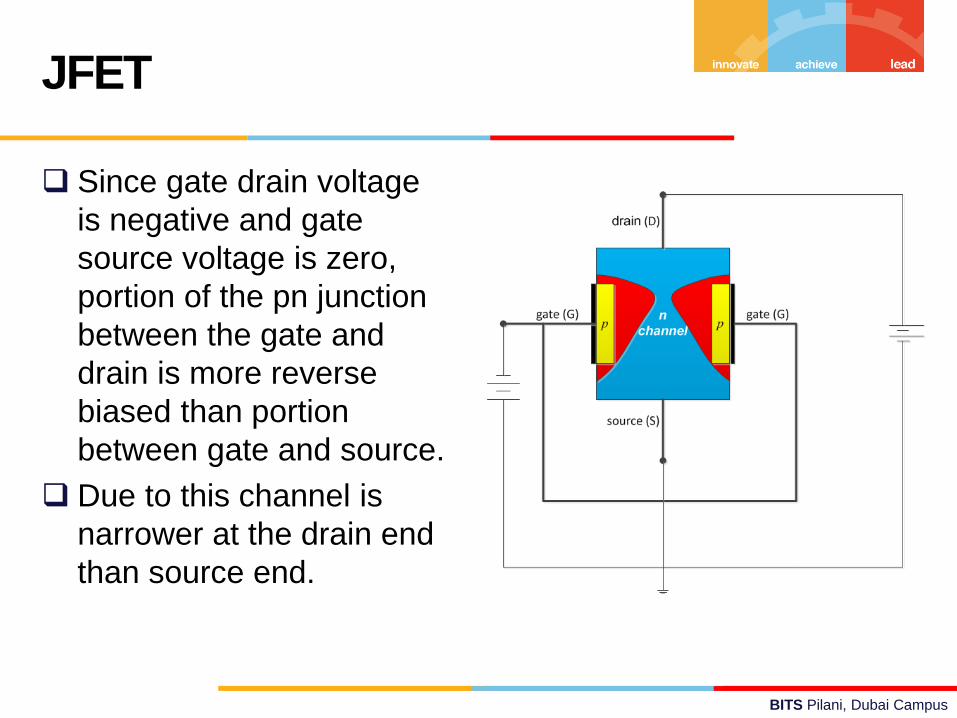
Since gate drain voltage
is negative and gate
source voltage is zero,
portion of the pn junction
between the gate and
drain is more reverse
biased than portion
between gate and source.
Due to this channel is
narrower at the drain end
than source end.
JFET
BITS Pilani, Dubai Campus
JFET
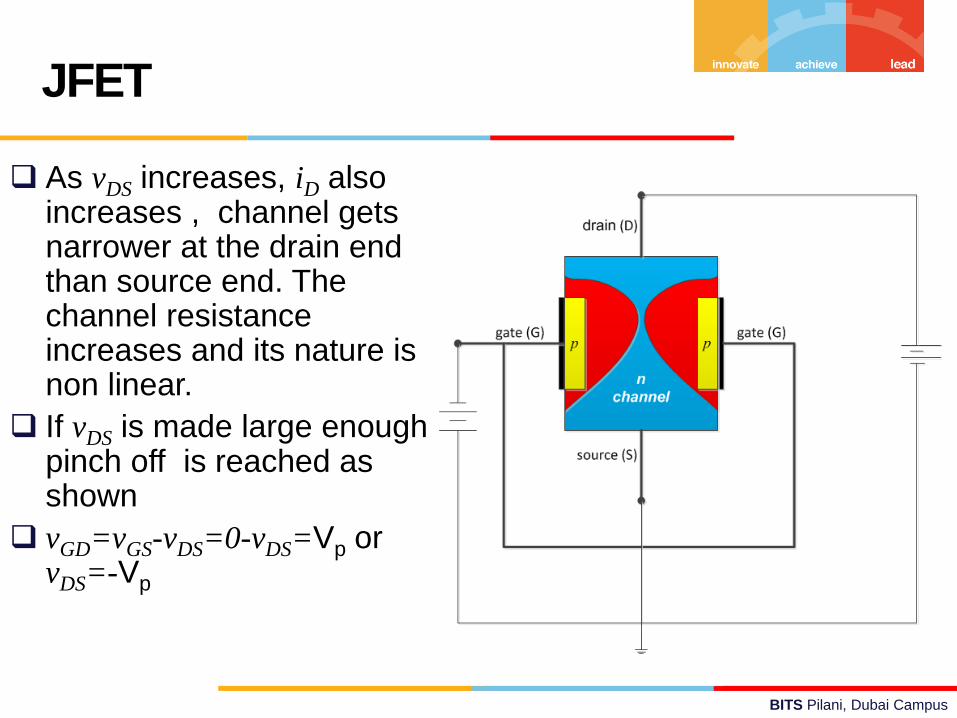
As vDS increases, iD also increases , channel gets narrower at the drain end than source end. The channel resistance increases and its nature is non linear.
If vDS is made large enough pinch off is reached as shown
vGD=vGS-vDS=0-vDS=Vp or vDS=-Vp
BITS Pilani, Dubai Campus
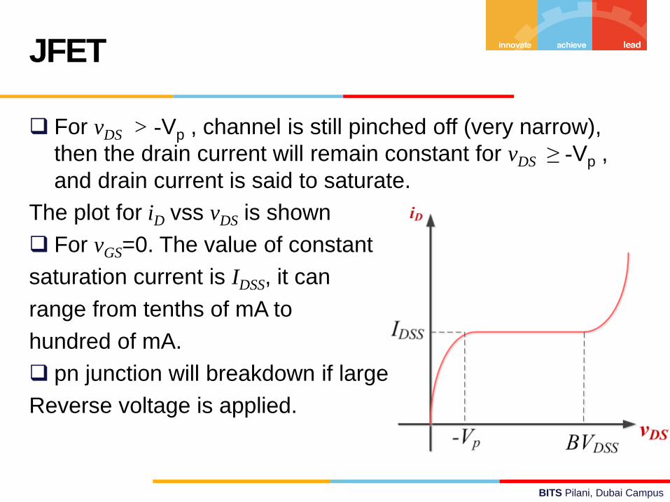
For vDS > -Vp , channel is still pinched off (very narrow),
then the drain current will remain constant for vDS ≥ -Vp ,
and drain current is said to saturate.
The plot for iD vss vDS is shown
For vGS=0. The value of constant
saturation current is IDSS, it can
range from tenths of mA to
hundred of mA.
pn junction will breakdown if large
Reverse voltage is applied.
JFET
BITS Pilani, Dubai Campus
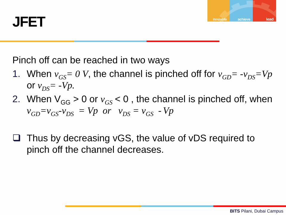
Pinch off can be reached in two ways
1. When vGS= 0 V, the channel is pinched off for vGD= -vDS=Vp
or vDS= -Vp.
2. When VGG > 0 or vGS < 0 , the channel is pinched off, when
vGD=vGS-vDS = Vp or vDS = vGS - Vp
Thus by decreasing vGS, the value of vDS required to
pinch off the channel decreases.
JFET

BITS Pilani, Dubai Campus
JFET (Drain characteristics)
IDSS= 12mA and
pinch off voltage is
Vp= -3V.
If vGS=0 V, channel
pinchoff when vDS=-
Vp=3V
If vGS=-1V, channel
pinchoff at
vDS = vGS - Vp =
-1+3=2V

BITS Pilani, Dubai Campus
The dashed curve is corresponding to vDS = vGS - Vp
To the right of this curve , (vDS > vGS - Vp ), The channel is
pinched off and this region is called as pinch off region or
saturation region. (active region).
To the left of this curve, (vDS < vGS - Vp ), the channel is not
pinched off and the region is called as ohmic region.
When the gate is sufficiently reverse biased , channel will
be totally eliminated for vGS < Vp, under this
circumstances increasing vDS, will not be sufficient to
produce a drain current. iD=0 and JFET is said to be in
cutoff.
JFET (Drain characteristics)
BITS Pilani, Dubai Campus
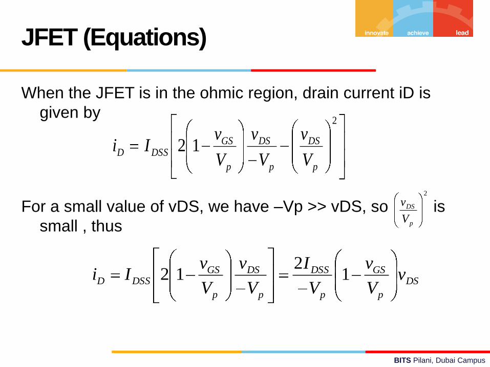
When the JFET is in the ohmic region, drain current iD is
given by
For a small value of vDS, we have –Vp >> vDS, so is
small , thus
JFET (Equations)
2
12p
DS
p
DS
p
GSDSSD
V
v
V
v
V
vIi
2
p
DS
V
v
DS
p
GS
p
DSS
p
DS
p
GSDSSD v
V
v
V
I
V
v
V
vIi 1
212
BITS Pilani, Dubai Campus
From which we can write
Thus for a small vDS , channel behaves as a linear resistor
rDS and is given by
When the JFET is in the active region , drain current is
JFET (Equations)
2
)(21
2
p
pGSDSS
p
GS
p
DSS
DS
D
V
VvI
V
v
V
I
v
i
)(2
2
pGSDSS
p
D
DSDS
VvI
V
i
vr
2
1p
GSDSSD
V
vIi
BITS Pilani, Dubai Campus
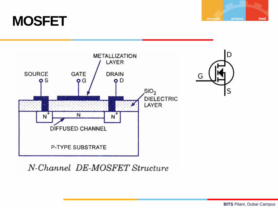
MOSFET
BITS Pilani, Dubai Campus
The resistance between reverse biased gate and source
is typically in megaohms.
For MOSFET, because of the insulation between gate
and the substrate , the resistance between the gate and
source is extremely high (in 1010 to 1015)
If vGS is made negative, the positive charges are induced
on the n channel, there by effectively narrowing it.
For varying value of vDS , the behavior of the device is
similar to the JFET.
Since it operates in the depletion mode, it is called as
depletion MOSFET.
MOSFET
BITS Pilani, Dubai Campus
MOSFET
BITS Pilani, Dubai Campus
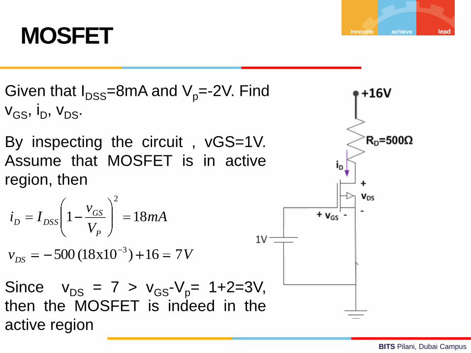
MOSFET
Given that IDSS=8mA and Vp=-2V. Find
vGS, iD, vDS.
By inspecting the circuit , vGS=1V.
Assume that MOSFET is in active
region, then
mAV
vIi
P
GSDSSD 181
2
VvDS 716)10x18(500 3
Since vDS = 7 > vGS-Vp= 1+2=3V,
then the MOSFET is indeed in the
active region