
JANUARY 1980 HEWLETTPACKARD JOURNAL · Editor, Richard P. Dolan • Contributing Editor, Howard...
32
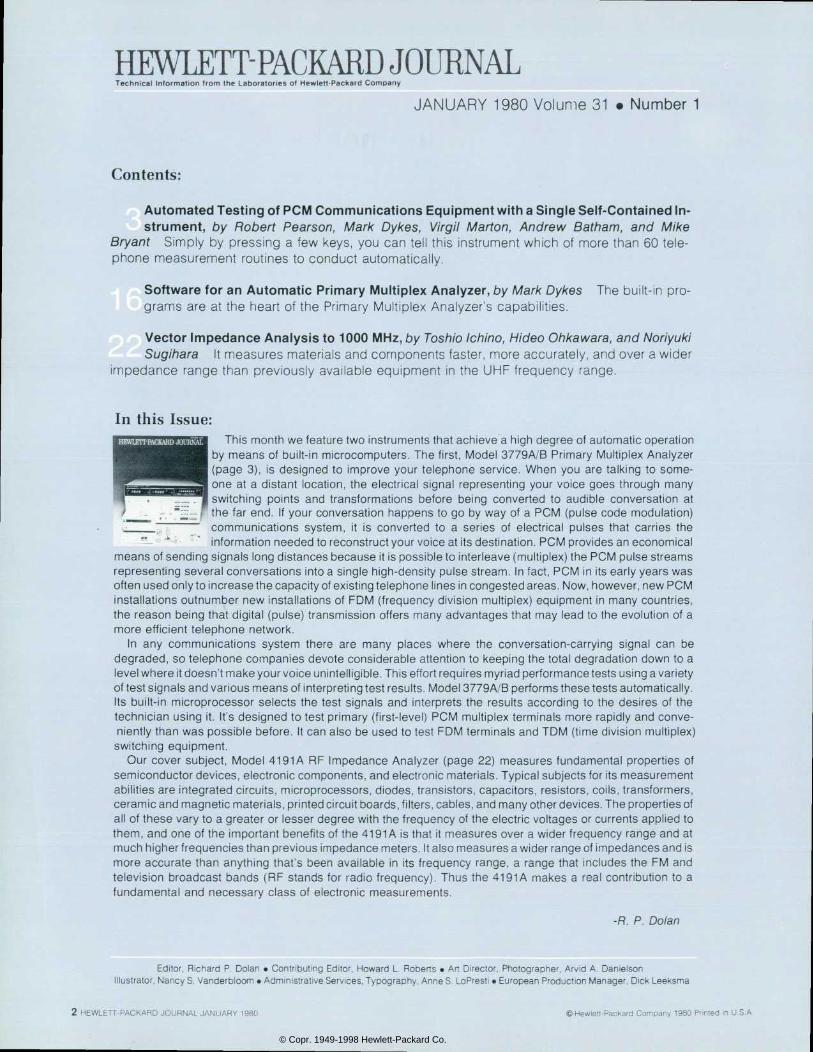
JANUARY 1980 HEWLETTPACKARD JOURNAL 4191* RF IMPEDANCE ANALYZER I - 1000 SBSB - eeee UNE OFF U a ON SRO LISTEN TALK REMOTE LOCAL loaauaoo DISPLAY A DISPLAY 0 PARAMETER 6 Ideg) 8 (radi r> G - O - f D * O f - a FREO,- 2 I 3 I SWEEP FREO / CALIBRATION DIGIT SHIFT flANQE TR1OOEO B BBVttWi *a» i © Copr. 1949-1998 Hewlett-Packard Co.
Transcript of JANUARY 1980 HEWLETTPACKARD JOURNAL · Editor, Richard P. Dolan • Contributing Editor, Howard...

JANUARY 1980
HEWLETTPACKARD JOURNAL
4 1 9 1 * R F I M P E D A N C E A N A L Y Z E R I - 1 0 0 0
S B S B - eeee UNE
O F F U a O N S R O L I S T E N T A L K R E M O T E L O C A L
l o a a u a o o
D I S P L A Y A D I S P L A Y 0 P A R A M E T E R
6 I d e g )
8 ( r a d i
r>
G - O - f D *
O f -
a F R E O , -
2 I 3 I S W E E P F R E O /
C A L I B R A T I O N D I G I T S H I F T f l A N Q E T R 1 O O E O
B BBVttWi
*a»
i
© Copr. 1949-1998 Hewlett-Packard Co.
HEWLETT-PACKARD JOURNAL Technica l In format ion f rom the Laborator ies of Hewlet t -Packard Company
JANUARY 1980 Volume 31 • Number 1
Contents:
Automated Testing of PCM Communicat ions Equipment with a Single Self -Contained In s t r u m e n t , b y R o b e r t P e a r s o n , M a r k D y k e s , V i r g i l M a r l o n , A n d r e w B a t h a m , a n d M i k e
Bryan t S imp ly by p ress ing a few keys , you can te l l t h i s i ns t rumen t wh ich o f more than 60 te le phone measurement rout ines to conduct automat ica l ly .
S o f t w a r e f o r a n A u t o m a t i c P r i m a r y M u l t i p l e x A n a l y z e r , b y M a r k D y k e s T h e b u i l t - i n p r o grams are at the hear t o f the Pr imary Mul t ip lex Analyzer 's capabi l i t ies .
Vec to r No r i yuk i Ana l ys i s t o 1000 MHz , by Tosh io I ch i no , H ideo Ohkawa ra , and No r i yuk i Sugihara I t measures mater ia ls and components fas ter , more accura te ly , and over a w ider
impedance range than prev ious ly ava i lab le equ ipment in the UHF f requency range.
In this Issue: Th is o f we fea tu re two ins t ruments tha t ach ieve a h igh degree o f au tomat ic opera t ion
I by means of bui l t - in microcomputers. The f i rs t , Model 3779A/B Pr imary Mul t ip lex Analyzer (page talk ing is designed to improve your te lephone service. When you are talk ing to some one at voice many locat ion, the electr ical signal representing your voice goes through many
I sw i tch ing po in ts and t rans fo rmat ions be fore be ing conver ted to aud ib le conversa t ion a t the far modulation) If your conversation happens to go by way of a PCM (pulse code modulation) commun ica t ions sys tem, i t i s conver ted to a se r ies o f e lec t r i ca l pu lses tha t ca r r i es the information needed to reconstruct your voice at i ts destination. PCM provides an economical
means of sending signals long distances because i t is possible to interleave (mult iplex) the PCM pulse streams representing several conversat ions into a single high-density pulse stream. In fact, PCM in i ts early years was often congested only to increase the capacity of existing telephone lines in congested areas. Now, however, new PCM instal lat ions outnumber new instal lat ions of FDM (frequency div is ion mult ip lex) equipment in many countr ies, the reason a tha t d ig i ta l (pu lse ) t ransmiss ion o f fe rs many advan tages tha t may lead to the evo lu t ion o f a more ef f ic ient te lephone network.
I n any commun ica t i ons sys tem the re a re many p l aces whe re t he conve rsa t i on -ca r r y i ng s i gna l can be degraded, a te lephone companies devote cons iderable a t tent ion to keeping the to ta l degradat ion down to a level requires it doesn't make your voice unintelligible. This effort requires myriad performance tests using a variety of test these and various means of interpret ing test results. Model 3779A/B performs these tests automatical ly. I ts bu i l t - in microprocessor se lects the test s ignals and in terprets the resul ts accord ing to the des i res of the technic ian using i t . I t 's designed to test pr imary ( f i rs t - level) PCM mul t ip lex terminals more rapid ly and conve niently division was possible before. It can also be used to test FDM terminals and TDM (time division multiplex)
swi tch ing equipment . O u r c o v e r o f M o d e l 4 1 9 1 A R F I m p e d a n c e A n a l y z e r ( p a g e 2 2 ) m e a s u r e s f u n d a m e n t a l p r o p e r t i e s o f
semiconductor devices, electronic components, and electronic mater ials. Typical subjects for i ts measurement abi l i t ies are integrated circuits, microprocessors, diodes, transistors, capacitors, resistors, coi ls, transformers, ceramic and o f mater ia ls , p r in ted c i rcu i t boards , f i l te rs , cab les , and many o ther dev ices . The proper t ies o f al l of these vary to a greater or lesser degree with the frequency of the electr ic voltages or currents appl ied to them, and one of the important benef i ts of the 41 91 A is that i t measures over a wider frequency range and at much higher frequencies than previous impedance meters. It also measures a wider range of impedances and is more accurate than anyth ing that 's been ava i lab le in i ts f requency range, a range that inc ludes the FM and te lev is ion broadcast bands (RF s tands for rad io f requency) . Thus the 4191A makes a rea l cont r ibu t ion to a fundamenta l and necessary c lass o f e lec t ron ic measurements .
-R. P. Do/an
Editor, Richard P. Dolan • Contr ibut ing Editor, Howard L Roberts • Art Director, Photographer, Arvid A. Danielson I l lustrator, Nancy S. Vanderbloom • Administrative Services, Typography, Anne S. LoPresti • European Production Manager, Dick Leeksma
2 H E W L E T T - P A C K A R D J O U R N A L J A N U A R Y 1 9 8 0 . Â © H e w l e t t - P a c k a r d C o m p a n y 1 9 8 0 P r i n t e d i n U S A .
© Copr. 1949-1998 Hewlett-Packard Co.
Automated Test ing of PCM Communicat ions Equipment with a Single Self -Contained Instrument Microprocessor cont ro l o f mul t ip le sources and detectors wi th in th is compact ins t rument ach ieves a new leve l o f automat ion for vo ice-channel measurements in PCM mul t ip lex equipment.
by Robert Pearson, Mark Dykes, V i rg i l Marton, Andrew Batham, and Mike Bryant
IN RECENT YEARS, the telephone network has seen a substantial growth in both the number of subscribers and the rate at which subscribers use its services. This
has prompted telephone operating companies to look to transmission and switching systems based on pulse code modulation (PCM) to provide the needed extra capacity. As a result, there has been a rapid growth in the manufac ture and installation of PCM multiplex equipment, and a corresponding demand for instruments that can test it.
A large number of performance characteristics that should be met between the analog input and analog output terminals (A-A) of a PCM multiplex system has been rec ommended by the International Telegraph and Telephone Consultative Committee (CCITT) and other international
bodies working on the standardization of PCM systems. In addition, discussion continues on the digital aspects of the multiplex and although recommendations have so far been limited mainly to the encoding and decoding characteris tics and the digital interfaces, it is clear that performance criteria for the transmit (A-D) and receive (D-A) halves will soon be defined. The development of an instrument that addresses itself to this large range of measurements — including many that are unique to PCM systems — has re quired a new approach to instrument design.
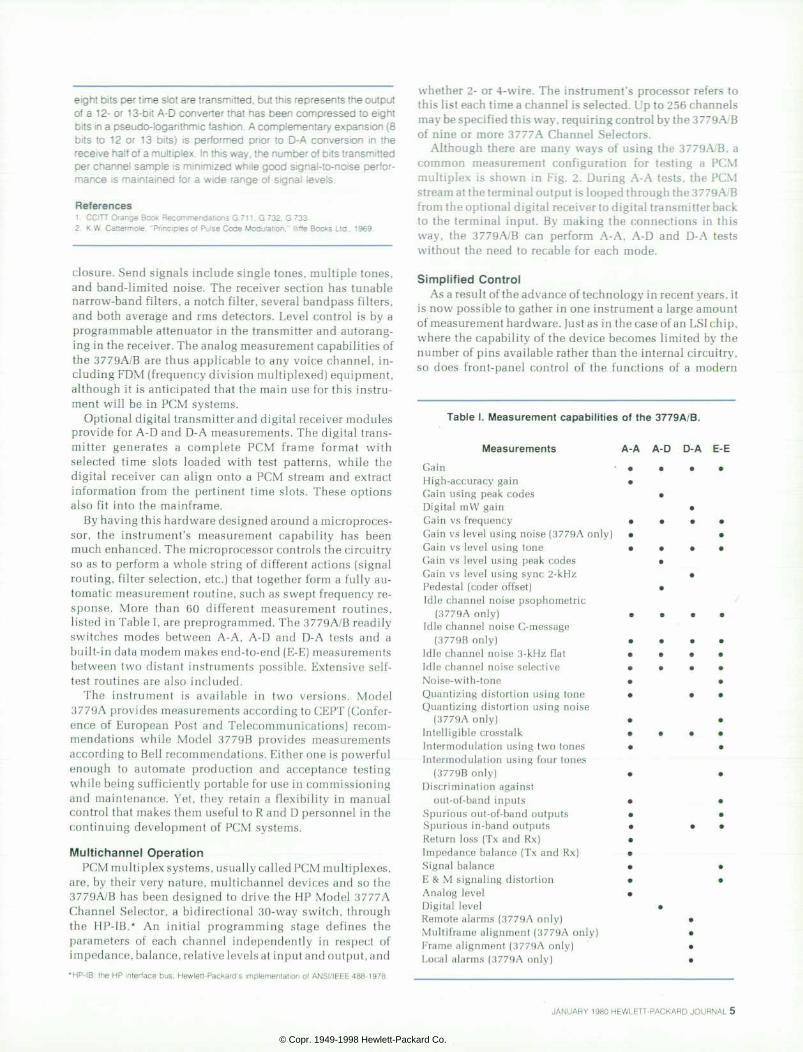
The Hewlett-Packard Model 3779A/B Primary Multiplex Analyzer, Fig. 1, is the result of this new approach. It is a complete measurement system containing both analog transmitter and receiver sections packed into a single en-
F i g . 1 . M o d e l 3 7 7 9 A / B P r i m a r y M u l t i p l e x A n a l y z e r p r o v i d e s mu l t imeasu remen t capab i l i t y f o r t e s t i n g P C M e q u i p m e n t . T h e 3 7 7 9 A s h o w n h e r e i s i n t e n d e d pr imar i ly for European 30-channel P C M s y s t e m s . T h e 3 7 7 9 B a c commoda tes the Nor th Amer i can 24-channel system.
JANUARY 1980 HEWLETT-PACKARD JOURNAL 3
© Copr. 1949-1998 Hewlett-Packard Co.

PCM Transmission Systems
The te lephone network has t rad i t iona l ly been an analog t ransmis s ion systems but s ince the mid-1 960's d ig i ta l t ransmission systems based as pulse code modulat ion (PCM) have become establ ished as an alternative to, or a substi tute for, analog systems. The advantages of PCM are c lear :
• Because of pulse regenerat ion in the repeaters, there is l i t t le pro g ress i ve de te r i o ra t i on o f a s i gna l on l ong -hau l t r ansm iss i ons , br inging long-distance te lephone cal ls up to the standard of local calls.
• S igna l ing in format ion (d ia l pu lses, r ing ing and engaged tones, e tc . ) is eas i ly handled, as is data t ra f f ic .
• Many channels (speech or data) can be t ime-division mult iplexed to share the same cab le pa i r , resu l t ing in subs tan t ia l sav ings in outs ide plant and an increase in network capaci ty to meet today's rap id g rowth in demand.
E x c h a n g e A E x c h a n g e B
P C M M u l t i p l e x
P C M M u l t i p l e x
a en
2 4 / 3 0 1
24/30
n ü D i g i t a l
R e g e n e r a t o r s
2 4 / 3 0
24/30
Q . C/)
Fig. 1. In a basic PCM transmission system, the dig i ta l s ignal (PCM s t ream) be tween the mul t ip lexes is regenera ted a t ap proximately one-mi le (1.6-k i lometre) in tervals.
A basic PCM transmission system is shown in Fig. 1 . The cable pair tha t now to car ry one speech channe l be tween two exchanges now carr ies 24 or 30. S ince th is cable was or ig ina l ly des igned to handle s i gna l s t ha t have a bandw id th o f 3 .4 kHz and now ca r r i es d i g i t a l s igna ls a t 1 .5 o r 2 Mb/s , the l ine equa l i za t ion ne tworks have been removed and rep laced by d ig i ta l regenera to rs . The cod ing permi ts
1 1 0 1 0 0 0 0 0 0 0 0 1
B i n a r y I
T e r n a r y A M I
H D B 3
J\rjl
J\rjl
T
B
Fig. 2. The AMI (alternate mark inversion) l ine code el iminates the dc component in the signal, al lowing dc power to be fed to the regenerators . Where no externa l c lock is supp l ied, c lock r e c o v e r y f r o m t h e s i g n a l i s h e l p e d b y u s i n g H D B 3 ( h i g h densi ty b ipo lar ) coding, which e l iminates long st r ings of O's . Any four consecutive O's are replaced by 000V or BOOV where V i s a r e c o g n i z a b l e c o d e v i o l a t i o n a n d B i s a m a r k t h a t i s inser ted to force successive v io lat ions to a l ternate in s ign. In Nor th Amer i ca , i t i s more common to use AZS (a l l ze ro sup pression) which replaces any d ig i t ized sample of e ight O's by 0000 0010 at the b inary leve l .
F r a m e 1 5 S p e e c h A l i g n m e n t C h a n n e l s
8 B i t s T i m e s l o t
3 2 T i m e s l o t s / F r a m e
8 0 0 0 F r a m e s / S e c o n d
M u l t i f r a m e A l i g n m e n t
1 5 S p e e c h C h a n n e l s
2 0 4 8 k b / s
Fig. 3 . The European 30-channel system uses a f rame a l ign ment signal in t ime slot 0 to identi fy each speech channel, and a mult i frame al ignment signal in t ime slot 16 to al low signaling in fo rmat ion assoc ia ted w i th each channe l to be d i s t r i bu ted throughout a 16- f rame mul t i f rame. The 3779A is des igned to interface with th is system.
dc power to be fed down the s igna l cab le (F ig . 2 ) . A m o d e r n p r i m a r y l e v e l m u l t i p l e x s a m p l e s e a c h o f 2 4 ( N o r t h
America) or 30 (Europe) audio speech channels at an 8-kHz rate. The samples a re d ig i t i zed and combined by t ime-d iv i s ion mu l t ip lex ing into a are digi tal pulse stream. On the receive side, the samples are demul t ip lexed and decoded back to ana log s igna ls .
A great deal of standardization has taken place on the details of the PCM equ ipment ,1 and two dominan t sys tems have emerged , bo th based upon an 8-kHz ra te fo r sampl ing the aud io s igna ls . C lear ly , t he re have to be some i den t i f i ca t i on b i t s i n t he PCM s t ream tha t enable the rece ive ha l f o f a PCM mul t ip lex to decode the ser ia l b i t stream. Figs. 3 and 4 il lustrate how this is achieved. In each case, only
I - O n e M u l t i f r a m e = 1 . 5 m s H
O n e F r a m e = 1 2 5 / ^ s
F r a m e A l i g n m e n t ' a n d
M u l t i f r a m e A l i g n m e n t
2 4 S p e e c h C h a n n e l s
8 B i t s T i m e s l o t I
2 4 T i m e s l o t s / F r a m e > 1 9 3 B i t s / F r a m e
I F r a m i n g B i t / F r a m e I
1 5 4 4 k b / s
Fig. 4. In the North American 24-channel system, f rame al ign ment and mul t i f rame a l ignment in format ion (more commonly referred to as terminal framing, FT, and signal ing framing, Fs) are both car r ied in a one-b i t -per - f rame sequence. S igna l ing i n f o r m a t i o n c a n b e a c c o m m o d a t e d b y s t e a l i n g o n e b i t p e r channel every 6th f rame. The 37798 has been developed for this system.
4 H E W L E T T - P A C K A R D J O U R N A L J A N U A R Y 1 9 8 0
© Copr. 1949-1998 Hewlett-Packard Co.
eight bits per t ime slot are transmitted, but this represents the output o f a 12- or 13-b i t A-D conver ter that has been compressed to e ight b i ts in a pseudo- logar i thmic fashion. A complementary expansion (8 b i t s t o 12 o r 13 b i t s ) i s pe r fo rmed p r i o r t o D -A conve rs ion i n t he receive half of a mult iplex. In this way, the number of bits transmitted per channel sample is min imized whi le good s igna l - to-no ise per for mance is mainta ined for a wide range of s ignal leve ls .
References 1 CCITT Orange Book Recommenda t ions G .711 , G .732 , G .733 . 2 . K W. Cat termole. "Pr inc ip les o f Pulse Code Modulat ion, " I l i f fe Books Ltd . , 1969
closure. Send signals include single tones, multiple tones, and band-limited noise. The receiver section has tunable narrow-band filters, a notch filter, several bandpass filters. and both average and rms detectors. Level control is by a programmable attenuator in the transmitter and autorang- ing in the receiver. The analog measurement capabilities of the 3779A/B are thus applicable to any voice channel, in cluding FDM (frequency division multiplexed) equipment, although it is anticipated that the main use for this instru ment will be in PCM systems.
Optional digital transmitter and digital receiver modules provide for A-D and D-A measurements. The digital trans mitter generates a complete PCM frame format with selected time slots loaded with test patterns, while the digital receiver can align onto a PCM stream and extract information from the pertinent time slots. These options also fit into the mainframe.
By having this hardware designed around a microproces sor, the instrument's measurement capability has been much enhanced. The microprocessor controls the circuitry so as to perform a whole string of different actions (signal routing, filter selection, etc.) that together form a fully au tomatic measurement routine, such as swept frequency re sponse. More than 60 different measurement routines, listed in Table I, are preprogrammed. The 3779A/B readily switches modes between A-A, A-D and D-A tests and a built-in data modem makes end-to-end (E-E) measurements between two distant instruments possible. Extensive self- test routines are also included.
The instrument is available in two versions. Model 3779A provides measurements according to CEPT (Confer ence of European Post and Telecommunications) recom mendations while Model 3779B provides measurements according to Bell recommendations. Either one is powerful enough to automate production and acceptance testing while being sufficiently portable for use in commissioning and maintenance. Yet, they retain a flexibility in manual control that makes them useful to R and D personnel in the continuing development of PCM systems.
Mult ichannel Operat ion PCM multiplex systems, usually called PCM multiplexes,
are, by their very nature, multichannel devices and so the 3779A/B has been designed to drive the HP Model 3777 A Channel Selector, a bidirectional 30-way switch, through the HP-IB. An initial programming stage defines the parameters of each channel independently in respect of impedance, balance, relative levels at input and output, and
•HP-IB: the HP interface bus, Hewlett-Packard's implementat ion of ANSI/IEEE 488-1978.
whether 2- or 4-wire. The instrument's processor refers to this list each time a channel is selected. Up to 256 channels may be specified this way. requiring control by the 3779A/B of nine or more 3777 A Channel Selectors.
Although there are many ways of using the 3779A/B, a common measurement configuration for testing a PCM multiplex is shown in Fig. 2. During A-A tests, the PCM stream at the terminal output is looped through the 3779A/B from back optional digital receiver to digital transmitter back to the terminal input. By making the connections in this way, the 3779A/B can perform A-A. A-D and D-A tests without the need to recable for each mode.
Simplif ied Control As a result of the advance of technology in recent years, it
is now possible to gather in one instrument a large amount of measurement hardware. Just as in the case of an LSI chip, where the capability of the device becomes limited by the number of pins available rather than the internal circuitry, so does front-panel control of the functions of a modern
Table I . Measurement capabi l i t ies of the 3779A/B.
Measurements Gain High-accuracy gain Gain using peak codes Digital mW gain Gain vs frequency Gain vs level using noise (3779A only) Gain vs level using tone Gain vs level using peak codes Gain vs level using sync 2-kHz Pedestal (coder offset) Idle channel noise psophometric
(3779A only) Idle channel noise C-message
(3779B only) Idle channel noise 3-kHz flat Idle channel noise selective Noise- with-tone Quantizing distortion using tone Quantizing distortion using noise
(3779A only) Intelligible crosstalk Intel-modulation using two tones Intel-modulation using four tones
(3779B only) Discrimination against
out-of-band inputs Spurious out-of-band outputs Spurious in-band outputs Return loss (Tx and Rx) Impedance balance (Tx and Rx) Signal balance E & M signaling distortion Analog level Digital level Remote alarms (3779A only) Multiframe alignment (3779A only) Frame alignment (3779A only) Local alarms (3779A only)
A - A A - D D - A E - E
JANUARY 1980 HEWLETT-PACKARD JOURNAL 5
© Copr. 1949-1998 Hewlett-Packard Co.

HP 3779A/B Primary Multiplex Analyzer
D i g i t a l A n a l o g R x T x
D i g i t a l A n a l o g T x R x
i ^ ^ ^ ^ H I I M B
HP 3777A Channel Selector
PCM Terminal
24/30
2 4 / 3 0 O - o
PCM Stream
HP-IB t
F i g . 2 . A t y p i c a l m e a s u r e m e n t c o n f i g u r a t i o n f o r A - A , A - D , a n d D - A t e s t i n g o f a P C M t e r m i n a l . C o n t r o l o f t h e 3 7 7 7 A C h a n n e l Selector anda printer is entirely by the 3779A/B by way of the HP inter face bus.
complex instrument become a real problem. The 3779A/B avoids the need for a potentially confusing array of dials and switches by using a special-purpose keyboard and an interactive CRT display. Ease of use is a major benefit result ing from this approach.
An important concept is that control of the 3779A/B is at the measurement level rather than the functional level. The user selects GAIN, for example, and enters frequency, level and so on instead of tuning an oscillator and setting an attenuator. An area of the front-panel keyboard (see Fig. 3) is designated MEASUREMENT. When the GAIN key is pressed, for example, a display is presented on the CRT that de scribes the measurement in terms of its parameters, in this case the number of channels to be tested, the signal frequency and level, and the result limits (Fig. 4). These default values for the parameters are preprogrammed, as is the structure of the measurement defining the selection of hardware functions and the sequence of actions within the measurement. Although the default values are stored in ROM the user can modify any parameter to suit the specific test procedure by using the cursor control keys to position
the cursor alongside the number of interest and pressing the numeric ENTRY keys.
Since the 3779A/B can perform so many measurements in each mode (A-A, A-D, D-A, E-E) a CRT display is used to permit a reduction in the number of MEASUREMENT keys. Each of the seven most-often-used measurements has a unique key while the OTHER MEAS key brings up the dis play of a list, or menu, of other measurements that are probably used less often. Fig. 5 shows the list for the other A-A measurements. Similar lists exist for A-D, D-A, and E-E measurements.
Microprocessor Control The use of processor control in the 3779A/B gives several
benefits in the running of measurements: • The complete measurement runs automatically, perform
ing a series of actions at each of a number of measurement points (e.g. different frequencies in a GAIN V. FREQ test) and, if required, repeating for each of a number of chan nels.
F i g . 3 . T h e k e y b o a r d o f t h e 3 7 7 9 A / B P r i m a r y M u l t i p l e x Analyzer.
C H f l N N E L : F R O M ! 1 S T E P 1 T O 3 0 F R E Q U E N C Y ( k H z ) : 0 . 8 2 L E U E L ( d B m 0 ) : 0 . 0 L O W E R L I M I T ( d B ) : - 0 5 0 U P P E R L I M I T ( d B ) : 0 5 0
Fig. 4. The display of the measurement parameters for a GAIN measurement in the A-A mode. The whi te square is a cursor that is used to change parameter va lues.
6 H E W L E T T - P A C K A R D J O U R N A L J A N U A R Y 1 9 8 0
© Copr. 1949-1998 Hewlett-Packard Co.

O T H E R M E f l S U R E M E N T S f t - f i
1 G R I N u L E V E L - t o n e 2 Q U A N T D I S T - t o n e 3 N O I S E W I T H T O N E 4 D I S C R I M I N R T I O N 5 I N B f l N D S P U R I O U S 6 O U T B f l N D S P U R I O U S 7 I D L E C H f t N N O I S E S E L 8 I D L E C H f t N N O I S E 3 k H z 9 R E T U R N L O S S
10 IMPEDflNCE BflLflNCE 11 SIGNftL BflLflNCE 12 E&M SIGNftLLING 1 3 L E V E L 1 - 4 H I G H f l C C U R f t C Y G R I N
E N T E R M E R S U R E M E N T N o :
Fig. 5. Typical OTHER MEAS display l is ts the measurements avai lable in addi t ion to those included in the MEASUREMENT sect ion of the keyboard.
Arithmetic is performed automatically by the micro processor to convert results to the most useful units, e.g. dB relative to ideal for a GAIN measurement, or dBmOp
for psophometrically weighted idle channel noise. • Testing is against programmed limits, with an indication
of PASS or FAIL for each result. • Pressing the PRINT key generates a fully formatted print
out of results on any 80-column, HP-IB compatible printer connected to the 3779A/B. A nonvolatile memory in the 3779A/B allows for storage
of a sequence of up to 68 measurements. By use of the INSERT key, any measurement with either default or mod ified parameter values can be added to a sequence. WAIT, REPEAT, PRINT and GO TO instructions, conditional on mea surement results, can be programmed (see Fig. 1) making the 3779A/B a self-contained automatic test system. Since the storage is nonvolatile, any programmed sequence is retained indefinitely, even with the instrument switched off. Measurements may be modified, deleted, or added to a sequence to suit a user's changing requirements, but for program security, this editing capability can be inhibited by using a four-digit numeric entry as a combination lock in conjunction with the PROGRAM LOCK key.
For cases where 68 measurements are insufficient, the contents of the memory can be transferred to and from the backup memory of an external controller (e.g. , a cassette in a
Faster Results with Automatic Measurements
T he automating of measurements is one of the main benefi ts to be g a i n e d f r o m p r o c e s s o r c o n t r o l i n a n i n t e l l i g e n t i n s t r u m e n t . T h e operator can be rel ieved of such tasks as sett ing frequencies, levels, e tc . , and these tasks can be s t rung together in to a preprogrammed measurement rout ine.
Consider the quantizing distort ion measurement outl ined in Fig. 1 . Th is measurement i s pe r fo rmed acco rd ing to the CCITT method1 which 800 brief ly, to measure the noise present in a bandwidth of 800 Hz to 2300 Hz result ing from the quantization of a noise signal that is limited to a band of 350 Hz to 550 Hz. The result is the ratio of signal to total d istor t ion power, wi th an appropr iate correct ion factor to re late th is to the fu l l PCM channe l bandwid th o f 300 Hz to 3400 Hz . The recommended l imi ts vary wi th the s ignal level .
Wi th the measurement parameters def ined in F ig. 1 the fo l lowing s teps a re pe r fo rmed au tomat i ca l l y by the 3779A/B fo r each o f 30 speech channels :
Q U f l N T D I S T - n o i s e
C H R N N E L : F R O M !
L E U E L < d B m 0 )
. S T E P 1 T O 3 0
L O W E R L I M I T ( d B )
F R O M S T E P TO
F R O M S T E P TO
-55. 0 5. 0
-40. 0 -34. 0 -27. 0 -25. 0
-10. 0 -6. 0 -3. 0
1 . Ins t ruc t the 3777A Channe l Se lec to r to se lec t the appropr ia te channel.
2 . Se t up the in te r face cond i t ions fo r tha t channe l ( i .e . , 600Ã1 o r 900Ãœ, balanced or unbalanced) and select the band-limited noise source as the st imulat ing s ignal .
3. With reference to the dBr levels of the channel under test, set the output signal level to -55 dBmO, the f irst point in the measurement "mask" .
4. In (350 analog receiver hardware, select the reference fi lter (350 Hz t o 550 Hz ) , t he rms de tec to r , and a su i t ab le ga te t ime f o r t he vol tage- to- f requency conver ter , then measure the s ignal level at the output o f the channel under test .
5 . Select now the measurement f i l te r (800 Hz to 3400 Hz) and mea sure the level o f d is tor t ion power at the channel output .
6 . Per form the appropr ia te ar i thmet ic , inc luding a bandwidth correc tion PASS and display the result in dB with an indication of PASS or FAIL relative to the mask limit.
7 . Repeat s teps 4 to 6 fo r t ransmi t s igna l leve ls o f -50 dBmO, -45 dBmO, etc. , as def ined by the measurement mask, displaying the resul t for each signal level .
F o r m e a s u r e m e n t p o i n t s l y i n g w i t h i n a s w e e p , e . g . - 5 5 t o - 4 0 dBmOand -25 to -10dBmO in F ig . 1 , the appropr ia te measurement l imit by each point within the sweep is calculated by the processor by interpolat ing between the l imi ts speci f ied for the sweep end points.
T h i s t h e r u n n i n g a u t o m a t i c a l l y , d e l i v e r s r e s u l t s a t t h e rate of about one every f ive seconds and wil l , therefore, characterize a channel wi th respect to the complete CCITT recommended quant i zat ion distort ion mask in about one minute. This represents a consid erab le improvement over ex is t ing manual tes t ar rangements .
Reference 1. CCITT Orange Book Recommendat ion 0 .131 .
Fig. 1. Measurements can be def ined in terms of a mixture of spot po in ts and sweeps.
'Mult iplex equipment signal levels are described in dBmO, where zero dBmO is the level of a s tandard s igna l a t tha t po in t in the sys tem The dBr leve l a t , say , the input o r ou tput o f a channe l , i s the d i f fe rence between 0 dBm and 0 dBmO at tha t po in t .
JANUARY 1980 HEWLETT-PACKARD JOURNAL 7
© Copr. 1949-1998 Hewlett-Packard Co.

desktop computer), giving the ability to store an almost infinite number of sequences of measurements.
Analog Transmi t ter and Rece iver The analog measurement circuits, illustrated in the block
diagram of Fig. 6, are simple in concept. Modular arrange ment and bus-structured processor control provide flexibil ity of hardware configuration, allowing efficient use of cir cuits for many different measurements. Signal routing at medium impedance is by means of bipolar transmission switches fabricated in thick film to HP design.
The t ransmi t te r sec t ion provides band- l imi ted pseudorandom noise (CCITT 0.131) in the 3779A or a four- tone signal (Bell Pubn. 41009) in the 3779B, in addition to single and double tones. The chosen output may be ad justed in level, impedance, and balance. It may also be routed to the receiver for calibration measurements.
The tones are generated by a synthesizer that is similar in concept to the synthesizer used in the HP Model 3770A Amplitude/Delay Distortion Analyzer,1 but provides three programmable frequencies simultaneously. These are a MAIN and an AUXILIARY signal, for use in 2- and 4-tone intermodulation tests, and a local oscillator signal for the first mixer of the selective detector in the analog receiver. Equally spaced samples of each waveform are calculated and converted to an analog voltage that is retained in a
sample-and-hold circuit until the next sample for that waveform occurs. The frequency is changed by altering the incremental change of phase between samples. A single digital-to-analog converter operates on a sample every 750 ns to generate a signal that is switched sequentially to separate sample-and-hold circuits for each output. Each sample-and-hold is followed by a suitable filter.
The noise output originates in a pseudorandom binary sequence generator and has a spectral line spacing of 4.77 Hz.
In the receiver section, after impedance matching and autoranging, the raw input signal is passed through filters specified for the measurement. Tunable 12-Hz and 40-Hz bandwidth filters use three stages of mixing with a local oscillator signal and filtering and provide an output at 326 Hz. Notch and bandpass filter characteristics are specified by measurement standards.
The output from the filters is restored in level by an autoranging amplifier and converted to dc by squaring rms or averaging detectors with selectable time constants. De tection is followed by a voltage-to-frequency conversion that involves gating a 1-MHz clock to produce a count proportional to sig-nal level.
A sine-to-square-wave converter that operates on the output of the autoranging amplifier, together with flexible counter control logic, provides combinations of clock and gating period that enable the counter to measure the level,
Analog Transmit ter
Analog Receiver •Self-Test Inputs Standard
Source
F i g . o f P r i m a r y b l o c k d i a g r a m o f t h e a n a l o g T x a n d R x s e c t i o n s o f t h e 3 7 7 9 A / B P r i m a r y Mul t ip lex Analyzer.
8 H E W L E T T - P A C K A R D J O U R N A L J A N U A R Y 1 9 8 0
© Copr. 1949-1998 Hewlett-Packard Co.

End-to-End Measurements
Product ion or acceptance tes t ing o f te lephone channe l banks is usua l l y done w i th the banks l ooped on themse lves back - to -back . This arrangement , i l lust rated in F ig. 2 on page 6, requi res only one 3779A/B.
S o m e t h e a n d m a i n t e n a n c e p r o c e d u r e s r e q u i r e i n s t e a d t h e t e s t i n g o f a n a c t u a l c h a n n e l b e t w e e n t w o p o i n t s w i t h o u t f a r - e n d loop-around. Th is conf igurat ion invo lves separate t ransmi t t ing and r e c e i v i n g e n d s w i t h c o m m u n i c a t i o n b e t w e e n t h e t w o . A p a i r o f 3 7 7 9 A / B i n s t r u m e n t s c a n w o r k t o g e t h e r t h i s w a y a u t o m a t i c a l l y , communicat ing over the channel under test . Measurements may be made in ei ther direct ion and resul ts may be displayed and/or pr inted at the master end (see Fig. 1) .
Serial
Channel Under Test
(4-wire)
Fig . 3 . End- to-end communicat ions c i rcu i ts .
T x Measurement
Circuits
In the 3779A/B, a lmost a l l A-A measurements may a lso be made end-to-end. The mult ichannel, sequence, and HP-IB control faci l i t ies are the same as for other modes. When the master instrument is given a R U N c o m m a n d , e x e c u t i o n o f a n e n t i r e s e q u e n c e c a n p r o c e e d automatical ly without operator intervention. The slave instrument may be unat tended.
In the E-E modes, al l software operat ions take place in the master instrument, which actual ly executes the measurement rout ines (Fig. 2) . When a run begins, the master instrument f i rst at tempts to estab l i sh two-way communica t ion w i th the s lave , scann ing a l l ava i lab le channels until i t receives a response. From the direction of testing, the master decides whether i tsel f or the s lave instrument is the t ransmit ter, and accordingly directs the hardware commands either to i tself or v ia communica t ions rou t ines to the s lave . Commands, resu l ts and test signals are passed back and forth to complete the measurement. The s lave ins t rument s imply executes hardware commands as they a re rece ived and i s unaware o f the par t i cu la r measurement be ing per formed. No sof tware operat ions are needed in the s lave.
E-E Communicat ion The end- to-end capabi l i ty o f the 3779A/B requi res no ext ra mea-
F ig . 1 . End- to -end measurement setup.
surement c i rcui ts. Rather, i t is based on informat ion processing and cont ro l , and in a p rocessor -based ins t rument these are eas i l y p ro vided.
T w o s t a n d a r d 1 C c h i p s a n d a s i m p l e f i l t e r a r e e n o u g h f o r t h e processor to transmit and receive asynchronous 600 bps FSK signals on the leve l under tes t , us ing ex is t ing measur ing c i rcu i ts fo r leve l a d j u s t m e n t , c h a n n e l m a t c h i n g , a u t o r a n g i n g , f i l t e r i n g a n d s i n e / square conversion (Fig. 3) .
The data carr ier is detected by a software rout ine that exploi ts the f lex ib i l i ty of the analog receiver to check the level and f requency of the incoming s ignal .
Signal paths wi thin the instrument are switched back and forth for measurement o r communica t ion as requ i red , under p rocessor con trol.
At the data- l ink level , the job of the processors at e i ther end is to e n s u r e i s c o m m u n i c a t i o n o f m e s s a g e s . T h e l i n e p r o t o c o l i s designed to tolerate delays and errors in transmission but i f the noise or loss in a channel is too bad to permi t communicat ion, then both instruments wi l l t ime out , re-establ ish communicat ion on channel 1, and cont inue the measurements on the next good channel . A "chan ne l sk ipped" message is pr in ted for the fau l ty channel .
Fig. 2. Automat ic synchronizat ion of E-E measurements.
JANUARY 1980 HEWLETT-PACKARD JOURNAL 9
© Copr. 1949-1998 Hewlett-Packard Co.

period, or frequency of the incoming signal. Two forms of averaging are present in the receiver: the
time constant of the detector, and the gating time during which the counter is enabled. For signals of known fixed period, e.g., pseudorandom noise or the 326-Hz output of the selective fi l ters, measurements can be significantly speeded by using a short detector time constant and allow ing the counter to integrate the varying detector output over an integral number of periods.
End-to-end communication over the channel under test is very s imply added to the instrument s ince the exist ing measuring circuits are already under microprocessor con trol and are thus capable of being controlled by another ins t rument tha t communica tes wi th the processor v ia built-in modems. Measurement Accuracy
The ins t rument i s des igned to compare s igna ls , fo r
example the s ignal received wi th that or ig inal ly sent . Therefore, the receiver's gain linearity defines the accuracy of the instrument. The absolute level of the transmitter output and the absolute gain of the receiver chain are both irrelevant. The combination of primary autorange, averag ing detector, and voltage-to-frequency converter together yields a basic accuracy of 0.04 dB for the comparison of two signals.
The instrument measures a signal in absolute terms by comparing it with a built-in ac reference available at the receiver input. This source is nominally I kHz at 3.535V rms, but if the user can measure its actual level to better than 0.02 dB, that value can be entered by way of the instru ment's front panel for enhanced accuracy.
For self test, the circuit arrangements needed for mea surement provide for back-to-back tests within the instru ment. Extra signal paths are included for fault isolation.
A Digital Attenuator with 1-dB Steps
One o f the requ i rements ¡n D-A (d ig i ta l - to -ana log) tes t ing in a primary mult iplex is a digit ized sine wave for frequency response and leve l tes t ing . The f requency synthes izer in the 3779A/B genera tes d i g i t i z e d s a m p l e s o f a s i n e w a v e t h a t a r e p r o c e s s e d t h r o u g h a digital-to-analog converter for use as the stimulus in analog tests. The d ig i t ized samples are used d i rec t ly fo r the D-A tes ts .
A second requ i rement i s to man ipu la te the d ig i t i zed samp les to syn thes i ze a t tenua t i on o f t he p ro to t ypa l s i ne wave . I n t he d ig i t a l d o m a i n , l e f t - t o - r i g h t s h i f t s o f e a c h s a m p l e w o u l d s y n t h e s i z e a t t e n u a t i o n i n 6 - d B s t e p s . H o w e v e r , a m e a n i n g f u l t e s t o f a P C M decoder requires f iner resolution than this. Level control over a 70-dB range in 1 -dB s teps was des i red fo r the 3779A/B.
For a d ig i ta l sample S, cons ider the fo l lowing equat ions:
S - 1 d B = 0 . 8 9 1 2 S = 0 . 8 9 1 8 ( 1 )
S - ^ S - ^ S - g ^ S = 0 . 8 9 0 6 8 = 0 . 8 9 1 3 ( 2 )
T h u s , a t t e n u a t i o n b y 1 d B ( i . e . , m u l t i p l i c a t i o n b y 0 . 8 9 1 ) c a n b e ach ieved by sub t rac t ing f rom samp le S a se r ies o f words tha t a re t h e m s e l v e s s h i f t e d v e r s i o n s o f S . E x p r e s s i o n s s i m i l a r i n f o r m t o equat ion (2) can be der ived for o ther va lues o f a t tenuat ion and, by accommodating up to 8 shifts ( i .e. S/256), an accuracy of 0.03 dB can be realized. In the 3779A/B, the samples S are 1 2-bit words, so 20-bit arithmetic is used to handle the sample and its 8-bit-shifted versions.
Input Sample
Fig. and Hardware organizat ion for attenuating by shif t ing and add ing.
T o c o v e r t h e l a r g e r a n g e o f a t t e n u a t i o n s r e q u i r e d , a " c o a r s e - p l u s - f i n e " a p p r o a c h i s u s e d . I n p u t s a m p l e s a r e i n i t i a l l y s h i f t e d t o g i v e a c o a r s e a t t e n u a t i o n i n 6 - d B s t e p s , a n d a f i n e cor rect ion (+2 dBto -3 dB) is then appl ied. The complete operat ion can be def ined mathemat ica l ly as :
OUTPUT = SS[1 ± J . J256;
Where Ss i s the o r ig ina l samp le S a f te r sh i f t i ng , and coe f f i c ien ts c - i to C8 have the value 0 or 1 as appropriate. I t is worth not ing that cumulat ive er rors due to the approx imat ion to 6 dB of each one-b i t shi f t ( instead of 6.0206 dB) can be cancel led in the f ine at tenuat ion stage.
Fig. the shows how the digital attenuator hardware is organized in the 3 7 7 9 A / B . A n a t t e n u a t i o n c o d e w o r d ( F i g . 2 ) i s g e n e r a t e d b y t h e p r o c e s s o r f o r u s e b y t h e c o n t r o l l o g i c . T h e c o d e w o r d f o r 1 5 - d B at tenuat ion is shown in Fig. 2.
The contro l log ic operates as fo l lows: 1 . Load reg is ter 2 w i th input sample S. 2 . R ight -sh i f t reg is ter 2 accord ing to the coarse at tenuat ion f ie ld . 3 . C l e a r r e g i s t e r 1 a n d p e r f o r m a n A D D . R e g i s t e r s 1 a n d 2 b o t h
now hold the shi f ted sample Ss. 4 . R igh t -sh i f t reg is te r 2 and scan the f ine a t tenuat ion coe f f i c ien ts
(CL C2 . . . ) unt i l a 1 is encountered. 5. Perform an addi t ion or subtract ion as def ined by the ADD/SUB bi t
in the at tenuat ion code word. 6 . Repeat s teps 4 and 5 unt i l a t tenuat ion is comple te .
'Add/Subtract
Coarse Attenuation Field
Number of Shif ts
C o a r s e : 2 S h i f t s = 2 x " - 6 d B " = - 1 2 . 0 4 1 d B F i n e : 1 - ( 1 / 4 + 1 / 3 2 + 1 / 1 2 8 ) = - 2 . 9 6 3 d B
-15.004 d B
Fig. 2 . The format of the at tenuat ion code word, shown here for 15 dB. The Vz term is never needed and is not inc luded.
1 0 H E W L E T T - P A C K A R D J O U R N A L J A N U A R Y 1 9 8 0
© Copr. 1949-1998 Hewlett-Packard Co.

Digital Transmitter and Receiver Adding the optional digital transmitter and receiver to
the 3779A/B provides the capability within one instrument of characterizing the analog-to-digital and digital-to-analog halves of a channel band separately. The digital ports of the instrument are designed to interface with the digital pulse stream conforming to the framing structures outlined in "PCM Transmission Systems," page 4.
Because of the marked differences between the European and North American systems it was necessary to define two different digital transmitters and receivers. Where the op portunity arises, however, as much commonality as feasible has been designed in. In a number of places wire links are used to program operation at the circuit-board level to either the European or North American standard, thus pro viding common boards for the 3779A and 3779B.
In both versions of the instrument, the digital receiver is designed to accept the digital pulse stream in the ternary alternate mark inversion form. The buffer amplifier on the digital inputs enables the 3779A/B to operate with cable losses of up to 6 dB. In addition, an extra 30 dB of gain may be inserted by means of a rear-panel switch to allow the instrument to operate with signals from a low-level monitor point.
The incoming pulses are buffered and converted from their ternary form to binary by means of two high-speed comparators. This binary stream is then fed to a clock ex traction circuit consisting of an injection-locked oscillator whose output may be used both to extract the data from the pulse stream and as the master clock for the digital receiver. Alternatively, the master clock may be derived from an external clock input applied to the rear panel.
In many European primary-level PCM systems, a form of data encoding called HDB3 is used to suppress strings of zeros. The 3779A decodes this format in its digital receiver. North American primary level PCM systems do not use HDB3-type line codes. Instead, an AZS (all zeros suppres sion) binary code is used which, because it is binary rather than ternary, does not involve line code violations and is not detectable at the receive end.
Framing The digital pulse stream in a PCM system has a very
definite format or frame structure. Before any useful infor mation can be extracted from the data stream it is necessary to align the receiver to the framing of the incoming signal. This is achieved by a synchronous state machine that can handle common channel signaling (CCS) or channel as-
E & M Signaling Measurements
Before any two subscribers can talk to each other over a telephone system, a signal path must be established between them. Information o n t h e n u m b e r d i a l e d , a l o n g w i t h r i n g i n g a n d b u s y s i g n a l s a n d metering, has to be passed between exchanges. In a PCM l ink this is done by us i ng t he s i gna l i ng channe l assoc i a ted w i t h each vo i ce channel.
Seve ra l t ypes o f s i gna l i ng a re i n common use . The 3779A/B i s d e s i g n e d t o i n t e r f a c e w i t h t h e m o s t c o m m o n f o r m , c a l l e d E & M signal ing. This form is a teletype-l ike signal based on two states: ON ( input and output s ink or source current) and OFF ( input and output open re lays, S ince a lo t o f s ignal ing equipment is bu i l t w i th re lays, the vo l tage leve l used i s the fu l l exchange ba t te ry vo l tage (abou t 50V). on bat tery vo l tage can be posi t ive or negat ive, depending on the system, and the ON state may be asserted either by pull ing the M input of the multiplex to ground, known as ground signaling, or pull ing t h e M i n p u t t o t h e b a t t e r y v o l t a g e , k n o w n a s b a t t e r y s i g n a l i n g . L ikewise the E output o f the mul t ip lex may go to bat tery or ground potent ia l , depending on the system in use.
The 3779A/B tes ts the s igna l ing channels o f a PCM mul t ip lex by
sending a square wave into the mult iplex Tx input, M, and comparing i t w i th the square wave received at the Rx s ignal ing output , E. Any di f ference in the mark/space rat io of the received signal is regarded as s igna l ing d is to r t i on wh ich , i f i t becomes too h igh , cou ld cause errors in the received data.
To avo id hav ing the opera to r p rog ram in to the 3779A/B exac t l y w h a t t h e l e v e l s i t s h o u l d t r a n s m i t a n d e x p e c t t o r e c e i v e , t h e 3779A /B ca r r i es ou t seve ra l t es t s au toma t i ca l l y t o asce r t a i n t he character is t ics o f the system under tes t before the actua l measure ment. These tests are as fol lows. First, the 3779A/B Tx output, M (on the rear panel ) , is set open c i rcu i t and the s tate of the 3779A/B Rx input, E (also on the rear panel), is monitored and stored as the OFF level . Next , the M output is pul led to ground. I f the E input changes state, then the mult ip lex uses ground signal ing and the new state of the E input is stored as the ON level. However, if there is no reply, then the M output is pul led to battery potential. I f the E input now changes state, then the mult ip lex uses battery s ignal ing and the new state of the E input is stored as the ON level.
If there was no change of state for either of the above then there is a
Exchange 1 Signaling Unit PCM Transmission
System
Exchange 2 Signaling Unit
Battery
Fig. 1 . Simpl i f ied E & M system.
JANUARY 1980 HEWLETT-PACKARD JOURNAL 11
© Copr. 1949-1998 Hewlett-Packard Co.

I f a sat is factory reply to one of the t ransmit ted levels is received, t h e n t h e s i g n a l i n g m e a s u r e m e n t b e g i n s . A s q u a r e w a v e p r o g r a m mab le the f requency and mark /space ra t io i s t ransmi t ted f rom the 3779A/B M ou tpu t us ing e i t he r g round o r ba t te ry as the ON s ta te depending on the result of the earl ier test. The E input of the 3779A/B looks only for the ON and OFF levels i t previously remembered, thus e l iminat ing spur ious resu l ts due to sp ikes or re lay contact bounce. The mark/space rat io of th is reconstructed square wave is t imed and ca lcu la ted by the p rocessor and the resu l t d isp layed on the CRT.
Because o f the low data ra te in the s igna l ing channe ls — each channel is selected once every 2 ms in CEPT systems and once every 1.5 ms falling Bell systems — there will be jitter in the rising and falling edges the the square wave. By averaging over several samples, the delay in both the r is ing and fa l l ing edges wi l l converge towards the same l imi t , thus tending to cancel out th is source of er ror .
A s impl i f ied E & M system is shown in Fig. 1. When the M input of Exchange 1 is connected to the bat tery vo l tage (bat tery s ignal ing) , the signaling bits in the PCM send l ink for that channel are set. These b i t s a r e d e c o d e d i n t h e m u l t i p l e x o f E x c h a n g e 2 a n d t h e o u t p u t t ransistor is turned on, pul l ing the E output high. Exchange 2 signals back in a s imi lar fashion.
A s imp le tes t se tup is shown in F ig . 2 . Th is a r rangement can be extended to mul t ichannel measurements by us ing a 3777A Channel Se lec to r . The equ iva len t c i r cu i t o f the 3779A/B s igna l ing tes te r i s shown. The processor se lects e i ther ground or bat tery s igna l ing by enabl ing ei ther S1 or S2, and generates the required code by turning the ou tpu t on and o f f a t t he requ i red ra te us ing S3 . The 3779A/B s igna l ing rece iver cons is ts o f two comparators that in form the pro-
F i g . 2 . E & M t e s t s e t u p i n t h e 3779A/B.
cessor of the vol tage level at the E input . To al low for posi t ive or negat ive battery vol tages, each switch is a
solid-state bidirectional switch of the type shown in Fig. 3. The control l ine in Fig. 3 turns on the t ransistors by way of the optoisolator . For posi t ive vol tages at the input , the current f low is through d iode D1, t rans is to r Q2, and d iode D4 to the ou tpu t . For nega t i ve vo l tages , cur rent f low is by way o f D3, Q2 and D2.
I n p u t O O Output
Fig . 3 . B id i rec t iona l sw i tch accommodates ba t te ry vo l tages of either polari ty.
sociated signaling (CAS) formats, depending on the posi tion of an internal link.
Because of the differences between the European and North American frame formats, this is one area that requires two separate circuits. For European PCM systems, the criteria for determining gain and loss of frame and multi- frame alignment are exactly defined in CCITT recommen dation G.732 and these criteria are adhered to in the 3779A.
For North American PCM systems, no such well defined standard exists. In the 3779B, if three or more alignment bits are in error in a group of eight alignment bits, frame align ment is then considered lost and is regained only after a run of six correct alignment bits. In the case of channel as sociated signaling, multiframe alignment is also moni tored and is considered lost if frame alignment is lost or if two consecutive multiframe alignment bits are in error. It is
1 2 H E W L E T T - P A C K A R D J O U R N A L J A N U A R Y 1 9 8 0
© Copr. 1949-1998 Hewlett-Packard Co.

regained only after a run of twelve consecutive multiframe bits are received correctly.
Once frame alignment, and if necessary multiframe alignment, has been achieved in the receiver, data may be extracted from the time slot of interest. This data can be analyzed in digital form by the instrument's processor or can be passed to the analog receiver via a D-to-A converter that operates on the bits corresponding to low-level signals. Converting the low-level signals to analog form has the advantage that the complex weighting filters already pres ent in the analog receiver may be fully used for "digital measurements" on noise and crosstalk.
In addition to extracting the data from the PCM pulse stream, the digital receiver also provides a number of flags to the processor so that the status of the incoming signal may be monitored. These include flags for loss of signal, loss of clock, loss of alignment, and the alarm indication signal (AIS) from the system under test, any of which could result in an invalid measurement if not detected.
Test Signals To perform D-A measurements, the digital transmitter
can generate a ternary PCM stream to the required format: 2.048-MHz 30-channel for the European 3779A, or 1.544- MHz 24-channel for the North American 3779B. Test data may be inserted into this PCM stream depending on the measurement to be made.
For tone-based tests (GAIN, GAIN V. FREQ., etc.) a digitally encoded sine wave is obtained from the frequency synthe sizer before the digital-to-analog conversion. It is selectable in frequency and level (see "A Digital Attenuator with 1-dB Steps," page 10) and may be inserted into any one time slot under processor control. Alternatively, data generated di rectly by the processor may be inserted into the time slot. This latter facility is used for such measurements as CCITT 1-kHz GAIN or 2-kHz GAIN V. LEVEL where the coded audio signal must be synchronous with the frame rate, or in frame and multiframe alignment tests (3779A only) where a number of different data strings are required and the reac tion of the equipment under test must be monitored.
For all measurements the data in the channels not under test — the "background PCM" — may be derived from one of two sources. Either the digital transmitter generates the complete PCM stream or it takes the signal presented to the digital receiver and retransmits it with the required test signal inserted in it. Internally generated background PCM usually is a pattern nominally equivalent to that generated by an idle channel, but for frame alignment tests, it consists of a pseudorandom binary sequence to simulate traffic.
The ability to retransmit the received PCM stream allows the user to generate any other background analog signal that may be desired, such as when measuring crosstalk. More importantly, it allows the digital path to be accessed for A-D and D-A tests or looped for A-A tests without the need to recable the instrument and equipment. With the transmitter running in this looped mode, its crystal oscil lator is disabled and the transmitter clock is derived from the receiver clock to maintain synchronization.
A further feature of the 3779A digital transmitter is its ability to generate the HDB3 line code if required. Similarly, the 3779B can suppress the all-zeros codes for North
American systems.
Single-Channel Codec Test ing In anticipation of the needs of current developments in
single-channel codecs and TDM (time division multiplex) switching equipment, a TTL interface is provided in the digital option. The data (Tx and Rx) is arranged as an 8-bit parallel or serial signal together with a synchronization signal at an 8-kHz rate. This general-purpose form enables simple external interface circuitry to be built for specific applications.
Self Test For self-test purposes, a means of automatically looping
the transmitter output back into the receiver is provided. By using this looped signal along with the various flags gener ated in the digital receiver, the instrument processor is able to test both the digital receiver and digital transmitter to a high level and isolate most malfunctions to a section of circuit.
The Processor System The processor chosen to control the PMA is HP's CMOS/
SOS 16-bit parallel microcontroller chip (MC2), a high per formance, low power consumption device.2 Due to the rela tively large number of real-time tasks involving manipula tions of the PCM data performed by the 3779A/B, this pro cessor replaces a large amount of dedicated digital hardware.
The processor section of the 3 7 79 A/B consists of the basic units of any computer system. The internal storage consists of: • 768 words of fast RAM (1 word = 16 bits), which is part of
the processor board. • 1024 words of nonvolatile RAM consisting of well-
proven ferrite cores, housed on a separate board. • 1024 bytes of DMA display RAM. • 32K words of 2K x 8 PROMs for system control and
measurement routines. • 2048 words of ROM available on the processor board for
self-test purposes. The 3779A/B is programmed manually from a keyboard
using an interactive display as a visual feedback device. The keyboard was implemented as a scanned matrix and uses the interrupt system to communicate with the proces sor. The display is based on a character generator that trans lates the ASCII characters contained in the 1 K-byte memory (to which the processor writes using the DMA technique) to a 9 x 7 dot matrix. The display memory provides the character codes needed for printing any display dump.
The processor controls the rest of the instrument via an instrument bus that is completely buffered from the proces sor bus. The instrument bus consists of six address lines, 16 data lines and one control line (strobe) and is regarded as part of the processor's I/O bus.
The 3779A/B can also communicate with the outside world. There are two basic means of establishing this com munication: 1. By way of the HP-IB, using the processor-to-HP-IB inter
face chip (PHI).3 This LSI device is part of the same CMOS/SOS family as the microprocessor itself. The
J A N U A R Y 1 9 8 0 H E W L E T T - P A C K A R D J O U R N A L 1 3
© Copr. 1949-1998 Hewlett-Packard Co.

HP-IB enables remote control of the 3779A/B as well as allowing the 3779A/B to control its own satellite devices (scanners, printer).
2. By way of the modem. An asynchronous, 600-bit/s modem is used by the 3779A/B to communicate with another 3779A/B on the line under test in order to per form the END-END class of measurements. A commer cially available FSK modulator/demodulator (MC14412) is used in conjunction with an asynchronous communi cation interface adapter (MC6850).
The HP-IB communicates with the processor using the in terrupt system, whereas the modem input is continually scanned while the processor is in its idle loop.
All processor boards communicate via the processor bus which consists of 16 address lines, 16 data lines, and 9 control lines. This bus is completely self-contained to en sure microprocessor availability for fault detection and lo cation for the rest of the instrument. The microprocessor
chip itself together with 2K words of ROM is buffered from the rest of the processor bus so it can be used to check the remaining components of the processor system individu ally. In this case, tests are controlled from a set of dual-in line switches on the processor board while four LEDs en code the results of different tests.
Acknowledgments Clearly, many people are involved during the develop
ment cycle of a product of this size and complexity. The authors would like to note the contribution of Rod May in providing broad technical experience as project leader dur ing the definition of the product and through to the lab prototype stage, and of Dave Leahy who deserves credit for the elegant and efficient packaging of the instrument. Robert Duncan and Alastair Sharp were responsible for the design of most of the analog transmitter and receiver sec tions, and Robin Mackay (product design) and David Guest
A B R I D G E D S P E C I F I C A T I O N S HP Model 3779A/B Pr imary Mul t ip lex Analyzer
Standard instrument provides analog-analog and end-end measurement capabi l i ty . Analog- d ig i ta l i n d ig i ta l -ana log capab i l i t i es a re op t iona l . The measurements a re summar ized in Table I , page 5.
Analog Transmit ter SINGLE TONE: 40 Hz to 40 kHz, ±50 ppm; 10-Hz reso lu t ion. PAIRS OF TONES: 40 Hz to 4 kHz, ±50 ppm, 10-Hz reso lu t ion . H A R M O N I C S , S P U R I O U S T O N E S : < - 5 5 d B . FLATNESS: ±0.01 dB (200 Hz to 4 kHz) ;
±0.05dB (40 Hz to 10 kHz); ±0.3 dB (40 Hz to 40 kHz).
NOISE SOURCE (3779A on ly ) : Mee ts CCITT Rec . 0 .131 . 4 -TONE SOURCE (3779B on ly ) : Mee ts BSTR 41009 . MAXIMUM OUTPUT LEVEL: +13 dBm ±0 .2 dB ( tones ) ;
+ 5 dBm ±0.2 dB (noise). M I N I M U M O U T P U T L E V E L : - 7 6 . 9 d B m . L E V E L R E S O L U T I O N : 0 1 d B . IMPEDANCE (ba lanced or unba lanced) : 600Ã! or 900f ! . MAXIMUM DC ISOLATION: ±56V
Analog Receiver M A X I M U M A C L E V E L : 1 2 V p - p . MAXIMUM DC LEVEL: ±56V. IMPEDANCE: 600Ã1 or 900Ã1. N O I S E F L O O R : < - 1 0 0 d B m p . SELECTIVE F ILTER: 12 -Hz o r 40 -Hz bandw id th . 3 - k H z F L A T F I L T E R : M e e t s B S T R 4 1 0 0 9 . QUANTIZ ING D ISTORTION: Mee t CCITT Rec . 0 .131 . ] P S O P H O M E T R I C F I L T E R : M e e t s C C I T T R e c . P . 5 3 . > 3 7 7 9 A o n l y . NOTCH F ILTER: 810 Hz . 4 - T O N E I N T E R M O D F I L T E R S : M e e t B S T R 4 1 0 0 9 . | C - M E S S A G E F I L T E R : M e e t s B S T R 4 1 0 0 9 . > 3 7 7 9 B o n l y . NOTCH F ILTER: 1010 Hz . INTERNAL STANDARD SOURCE: 3 .535V rms ±0 .2%.
E & M Signal ing O U T P U T
SIGNAL FREQUENCY: 5 Hz to 20 Hz , 1 -Hz reso lu t ion . DUTY CYCLE RANGE: 20% to 80%, 10%-s teps . MAXIMUM DC RANGE: ±56V. MAXIMUM CURRENT OUTPUT: ±100 mA.
INPUT INPUT IMPEDANCE: 50 k f l to ' /2Vbat te ry . DC OPERATING RANGE: ±56V (maximum), ±20V (min imum). INPUT S IGNAL FREQUENCY: 5 Hz t o 20 Hz . A L L O W A B L E C O N T A C T B O U N C E : 3 m s ( m a x i m u m ) .
Digital Transmitter P C M F R A M E F O R M A T : M e e t s C C I T T R e c o m m e n d a t i o n G . 7 3 2 ( 3 7 7 9 A ) o r R e c o m m e n
dat ion G.733 (3779B). S IGNAL ING: CAS o r CCS. CODING: HDB3 o r AMI (3779A) : AMI o r AZS (3779B) . OUTPUT IMPEDANCE: 75!1 unba lanced (3779A) ; 100Ã1 ba lanced (3779B) . S Y N T H E S I Z E D T O N E T E S T S I G N A L :
FREQUENCY RANGE: 40 Hz to 3 .5 kHz, ±50 ppm, 10-Hz reso lu t ion .
As for Digi tal t ransmitter.
LEVEL RANGE: +3 to -64 dBmO, 1 -dB reso lu t i on . COMPRESSION CHARACTERISTIC: A- law (3779A); /¿- law (3779B).
OTHER TEST SIGNALS: Processor-generated 8-bi t words at maximum word rate 1 word/frame. TEST S IGNAL LOCATION: Any one t ime s l o t .
Digital Receiver P C M F R A M E F O R M A T : SIGNALING: CODING: INPUT IMPEDANCE: RECEIVER CLOCK: Recovered o r ex te rna l . F R A M E A L I G N M E N T : A u t o m a t i c . MULT IFRAME AL IGNMENT (CAS on l y ) : Au toma t i c . TEST S IGNAL SELECTION: Con ten ts o f any one t imes lo t . MAXIMUM WORD RATE: 1 wo rd / f r ame . T I M E S L O T T R A N S L A T I O N M A P P I N G :
3779A: Contents TS(n), TS(n + 16) exchanged. 3779B: Conten ts TS{n) , TS(n+1) exchanged, fo r n an odd number .
Single-Channel Interface FORMAT: 8 b i ts ser ia l (o r para l le l ) + sync s igna l . WORD RATE: 1 word / f rame. LEVELS: TTL. INPUT IMPEDANCE (each l i ne ) : 100 f l to 3 .5V.
General P O W E R S U P P L Y : 1 1 5 / 2 3 0 V a c , + 1 0 - 2 2 % , 4 8 t o 6 6 H z , 1 5 0 V A . S IZE : 234 mm H x 426 mm W x 603 mm D (9 .3 x 16 .8 x 23 .8 Â ¡n ) . WEIGHT: 25 kg (55 Ib ) . OPERATING TEMPERATURE: O to 55=C. CONNECTORS:
ANALOG TX, RX ( f ron t and rear ) : 3 -p in S iemens (3779A) ; WECO 310 (3779B) . E & M SIGNALING: B ind ing posts . STANDARD SOURCE OUTPUT: 50Ã1 BNC.
Options 3779A OPTION 001:
As 3779A standard, p lus d ig i ta l TX, RX. C O N N E C T O R S : 7 5 n B N C ( a l l P C M i n t e r f a c e s ) ; 3 7 - w a y D - t y p e ( S i n g l e C h a n n e l
Interface). 3779A OPTION 002:
As 3779A Option 001 , except replace al l 75fl BNC connectors with Siemens 1 .6 mm 75ÃL 3779B OPTION 001:
As 3779B standard, p lus d ig i ta l TX, RX. C O N N E C T O R S : W E C O 3 1 0 ( a l l P C M i n t e r f a c e s ) ; 3 7 - w a y D - t y p e ( S i n g l e C h a n n e l
Interface). PRICES IN U.S.A. : Mode l 3779A/B, $22,810; op ts 001 and 002, $2285. M A N U F A C T U R I N G D I V I S I O N : H E W L E T T - P A C K A R D L T D .
South Queensfer ry West Lo th ian EH309TG Scotland
1 4 H E W L E T T - P A C K A R D J O U R N A L J A N U A R Y 1 9 8 0
© Copr. 1949-1998 Hewlett-Packard Co.

(analog circuits) helped ease the instrument into produc tion. Continuous support in a variety qf tasks came from Andy Horsburgh and Dave Jelfs with Stuart Ross and, lat terly, Colin Deighton covering production engineering considerations. Of the many others who contributed, men tion must be made of Peter Huckett, who was involved in the definition stage and has covered the market aspects, and of George Cooper for his many inputs regarding the testing of the instrument.
References 1. D.H. Guest, "Simplified Data-Transmission Channel Measure ments," Hewlett-Packard Journal, November 1974. 2. B.F. Forbes, "Silicon-on-Sapphire Technology Produces High-Speed Single-Chip Processor," Hewlett-Packard Journal, April 1977. 3. J.W. Figueroa, "PHI, the HP-IB Interface Chip," Hewlett- Packard Journal, July 1978.
Mike Bryant Mike Bryant jo ined HP in 1977 af ter re ceiving his B.Sc. in electronic engineer ing at Southampton Univers i ty . He worked on the d ig i ta l par t and some of the measurement sof tware of the 3779A/B. Twenty- three and s ingle, Mike's main interest is car rallying. He is present ly bu i ld ing a new ra l ly car and looking for sponsorship to enable him to compete in the Br i t ish Forest Ral ly Championsh ip . H is o ther in te res ts in c lude rock mus ic and modern ba l le t .
Andrew Batham Born in Surrey, England, Andy Batham gained his B.Sc. from the University Col lege of North Wales before joining HP at South Queensferry , Scot land in 1973. He worked in R & D on a number o f pro jects before jo in ing the 3779A/B team to tack le the d ig i ta l hardware. Andy , who i s mar r ied and has two young ch i ldren, has spent much of h is spare t ime recent ly bui ld ing a garage. He also enjoys orienteering and boating when car and house repa i rs permi t .
Robert Pearson Rob Pearson jo ined HP at South Queensferry in 1 973 and worked on the 3780A Pat te rn Genera tor /Er ror Detec to r . He became pro jec t leader fo r the 3779A/B af ter be ing invo lved in the ear ly work on i ts d ig i ta l hardware and related measurement software. Rob is a graduate of Glasgow Universi ty (B.Sc.) and Her io t -Wat t Univers i ty , Edinburgh (M.Sc.) . In his spare t ime he plays gol f and badminton and is se l f -suf f ic ient in
j h o m e - b r e w e d b e e r . R o b a n d h i s w i f e have one son and one daughter .
Mark Dykes A nat ive o f G lasgow, Scot land, Mark Dykes s tud ied eng ineer ing a t Jesus Co l l ege , Cambr i dge (MA) , and man agement at Glasgow Universi ty (DMS). Joining HP Ltd. in 1973 at the inception o f the 3779 pro ject , he cont r ibuted hardware to ear ly pro to types before work ing on suppor t and app l i ca t ions software for the f inal versions. Outside HP, Mark en joys s ing ing c lass ica l choral works and can be persuaded to g ive a "b law" on the bagpipes. A lo t o f h is t ime goes to he lp ing run youth camps and work ing w i th a var ie ty o f
à Christian organizations. In the summer, Mark l ikes v is i t ing h is grandparents in Swi tzer land or navigat ing England's historic canal system in a tradit ional sixty-foot narrowboat.
Virgi l Marion [ Virgi l Marton was born in a remote cor
ner of Transylvan ¡a (Romania) and came to Br i ta in in 1968 to s tudy comput er sc ience at Manchester Univers i ty . Af ter graduat ion, he worked in comput er system design for a large mainframe manufacturer . When he jo ined HP Ltd. in 1976, the 3779A/B was just enter ing i ts lab proto type s tage and h is main
I work was on the micropocessor control of the inst rument . Since then, he has worked on an invest igat ive pro ject in da ta commun ica t ion . Dur ing the ho l i days, Vi rg i l and his wi fe enjoy v is i t ing d i f ferent wine-producing countr ies and
joining in the local customs. Otherwise, reading and nature walks f i l l most of h is spare t ime.
JANUARY 1980 HEWLETT-PACKARD JOURNAL 15
© Copr. 1949-1998 Hewlett-Packard Co.

Software for an Automatic Primary Multiplex Analyzer by Mark Dykes
THE SOFTWARE in the 3779A/B had to meet two ob jectives: (1) to add intelligence to the powerful hard ware to furnish high-level solutions to specific mea
surement problems: and (2) to provide a friendly front panel that nevertheless allows the operator access to the full potential of the instrument. The control program is therefore quite complex, occupying 34K words of 16-bit memory. The main elements of the program are: • The keyboard/display operating system • Data tables • The measurement package • The self-test package • The HP-IB package.
Apart from the table area, the memory contains two kinds of code. Central service, speed-critical, and processor self- test routines are assembled into machine code. The mea surement package and instrument self-test routines are written in a high-level language and compiled into inter mediate code that is interpreted as it is run.
Traditional instruments measure continually, and their controls can be altered while they are running. The 3779A/B, by contrast, is a menu-controlled instrument with RUN and STOP keys. After switching the instrument on, it is normal to program it as desired (in the STOP state) , and then to press the RUN key. The measurements) specified are carried out (in the RUN state), and afterwards the instrument reverts to the STOP state. This division is basic to the organization of
the control program.
The Keyboard-Display Operat ing System The 3779A/B is capable of more than 60 measurements
with different types and numbers of parameters (i.e., level, frequency, limits, etc.). It can contain descriptions of 256 channels, store up to 68 measurements in user-defined se quences, and keep information on the test and HP-IB con figurations. Because of the volume of information to be handled, the entry and display system is cursor-controlled and highly interactive.
Information is entered by calling up the appropriate dis play and moving the cursor alongside the field of interest. As a value is keyed in, the numeric entry routines continu ally check it against upper and lower limits, and prompt the user with a message containing the relevant limit value if a mistake is made. In this case, the cursor freezes and flashes, and display changes are inhibited if necessary until a cor rect entry is made.
Keys are provided to edit parameter masks and measure ment sequences, and a FROM-STEP-TO format is available for swept parameters.
The mode and control states of the 3779A/B are always present in inverse video at the bottom of the screen.
Data Tables The details of display formats are held in ROM in the form
C o m m o n Tables
R O M
Strings, w i t h T y p e a n d
Cursor Co lumn
Defaul t Va lues and Ent ry L imi ts
Measurement Tab les
State Var iables
Measurement Tab le Pointer (MTP)
Display Recipe Pointer
Measurement Rout ine
Display Recipe
Display Recipe
Entry Pointers Current Entry
Position
Scratch Pad
RAM
Current Entry Memory Indexes Parameter
Va lue List
CRT
Fig. 1 . Display recipes di rect the assemb l i ng o f da ta f o r p resen ta t ion on the CRT.
1 6 H E W L E T T - P A C K A R D J O U R N A L J A N U A R Y 1 9 8 0
© Copr. 1949-1998 Hewlett-Packard Co.

Nonvolat i le Mem
Ü 5.8 in E
TJ S
I
Sequence R e c o r d < (
Current Sequence Measurement
Indexes
RAM
Measurement Record Pointer
and MTP
Measurement Record
of display recipes that are designed to be efficient for the more common types — allowing sharing of strings and so on — but that are also flexible to accommodate exceptions.
The first step in calling up a new display is to create a list of the requisite numeric values in a scratchpad area of RAM (Fig. 1). For a new measurement display, these values are default parameter values extracted from ROM via the dis play recipe, also in ROM. Thereafter, a common routine reads the display recipe in conjunction with the parameter list associating strings and numbers on the CRT screen. After the display is complete, keyboard modifications to the numbers displayed are also recorded in the scratchpad.
If a measurement display is present and a RUN command is given, the relevant measurement routine is found through the measurement table, and run in accordance with the associated descriptor.
A measurement in the scratchpad can be run as described, or saved by storing it in the sequence area in nonvolatile memory (Fig. 2). This area is organized as four sequences of 17 measurements that can be linked together to make one long sequence. Because sequences vary in length and mea surements have different numbers of parameters, the se quences are stored as records of arbitrary length. The num ber of measurements that can be stored depends on their complexity, because the size of the nonvolatile memory (NVM) is limited. The sequence area is repacked when ever a measurement is deleted from a sequence.
A portion of the NVM is used as a system area. This area contains information like the HP-IB address of the instru ment, the user-measured value of the instrument's standard source, channel descriptions, and other test configuration data. An interesting feature is the software lock mechanism, designed to prevent unauthorized alteration of user- defined information. Combinations can be entered to con trol access to individual sequences, or to disable all keys except RUN, STOP and DISPLAY keys. Locking the keyboard in this way limits the operator to executing exactly the stored sequence, a valuable feature in a production-test environment.
The NVM contains in its system and sequence areas all the user-defined information in the instrument. This infor mation or parts of it can be transferred over the HP-IB to and
Fig. 2 . The nonvolat i le read-wr i te m e m o r y h o l d s v a r i a b l e - l e n g t h sequences t ha t can be l i n ked t o make one long sequence .
from of external controller, so that the entire "character" of the instrument can be saved, restored, or copied.
Having both scratchpad and sequence areas gives the user several ways of working. Pressing a MEASUREMENT key or extracting a measurement from a sequence creates a record in the scratchpad that the user can modify and/or run on its own without affecting the contents of the sequence. New measurements can be added to the end of the sequence and measurements already in the sequence can be ex tracted, modified and replaced in the same order (Fig. 3).
Measurement Rout ines The 3779A/B makes measurements on voice frequency,
signaling, and first-order PCM signals. Most of the mea surements need only a little processor bandwidth, so it was possible to write them in a slow, interpretive high-level language. They had to be read and understood by hardware designers and test engineers, so legibility was useful at the writing stage. It was also helpful to have the complex mea surement hardware interactions amenable to debugging by means of the software trace embedded in the interpreter.
The quantizing distortion measurement described on page 7 under "Faster Results with Automatic Measure ments" shows what a typical measurement routine does. Each pass through the routine represents a single measure ment point, while the run-time system processes loops for point repetition, parameter sweeps and channel sweeps. When a sequence is run (Fig. 4), measurement records are brought from the sequence area to the scratch pad one by one as required.
Each type of measurement, for example GAIN, can run in up to four modes (A-A, A-D, D-A and E-E). The routines for different modes share as many subroutines as possible, and in fact A-A and E-E routines are combined since A-A mea surements are made up of transmitter and receiver opera tions that can be viewed separately even though they are carried out in one instrument.
In A-D measurements, an analog stimulus is applied to a channel bank and the received signal is a stream of PCM words at frame rate, i.e., one every 125 ¡JLS. The 3779A/B processor calculates the power represented by these words in real time. Although this is a high-bandwidth task, writ-
J A N U A R Y 1 9 8 0 H E W L E T T - P A C K A R D J O U R N A L 1 7
© Copr. 1949-1998 Hewlett-Packard Co.

Tables
MEASUREMENT) Key
Parameter Modif icat ions via the Keyboard i i M E A S P A R A M
Key
Measurement Record
INSERT Key ( O l d M e a s u r e
ment)
ROM
Run System Measurement Control
RAM Scratchpad
INSERT Key ( N e w M e a s u r e
ment)
Current Measurement
Sequence Area
NVM
Fig . 3 . The keyboard can be used to se lec t , modi fy , and run measurements either from the sequence area or fresh from the tables. New measurements may be added to the sequence or ex is t ing ones modi f ied.
ten in assembly language with attention to execution times and interrupt handling, the software implementation saves hardware in the digital receiver and allows the measure ment algorithms to be adaptive. Some D-A measurements are made using tones at a submultiple of the PCM sampling frequency. These measurements use the processor in real time, generating a pattern of PCM words that is synchron ous with the frame structure of the digital signal.
Submultiple frequency digital tones must be synchro nous, otherwise phase beating occurs and results are not repeatable. The programming problem here is that the main analog receiver routines cannot accommodate the simul taneous generation of a PCM word every 125 /us. Accord ingly, a dedicated analog receiver routine is used, written in the form of an assembly language loop. It generates a PCM word every frame. The processor can generate flexible digi tal output signals to test the framing, error, and alarm logic of the receive sections of channel banks. These capabilities would be difficult to match in hardware. Analog Receiver Rout ines
At the heart of the measurements are the receiver routines. These have a software resolution of 0.0025 dB. The main analog receiver routine is drawn in Fig. 5. Its first job is to have the input signal amplified to the level required by the receiver, without overloading. This in itself is a substantial task, since the instrument has to cope with badly asymmetric signals and face either polarity of a dc signaling voltage of up to 56V across its input. Higher and lower positive and negative threshold detectors show whether or not the signal has settled symmetrically and whether it is the right level. With the kind of time constants involved, the routine has to wait up to 7.5 seconds for asymmetry to disappear to be able to accommodate twice 56V. the symmetrical settling takes place within this time, the routine proceeds immediately. Otherwise, it assumes the signal itself is asymmetric and downranges if necessary. Once the receiver filter has settled to some extent, the sec ondary autorange operates on its output, and after a further delay for the final settling of filter and detector, the counter is read. Digi ta l Receiver Rout ines
Readings of digital level are made in real time by the
Fetch New Measurement Record
Initialize Instrument Mode
Initialize for New Measurement
•i Initialize for
New Channel
Se t "New Channe l"
Measurement Routine
Select Channel
C lear "New Channe l"
Make Measurements for Current Point
F i g . 4 . T h e m e a s u r e m e n t r o u t i n e e x e c u t e s o n c e f o r e a c h measurement po in t . I t i s enc losed by four program loops.
1 8 H E W L E T T - P A C K A R D J O U R N A L J A N U A R Y 1 9 8 0
© Copr. 1949-1998 Hewlett-Packard Co.

Software Development At the t ime the HP SOS MC2 was chosen as the processor for the
3779A/B, no sof tware deve lopment too ls ex is ted that would run on the lab computer system at Hewlet t-Packard Ltd. in Scot land, where the ins t rument was des igned. S tar t ing f rom scra tch , there fore , we developed our own home-grown support tools that included features des igned to ease sof tware deve lopment .
A large program must be generated in blocks so that changes can be made with a minimum of rework. This is true during development, where a 1K word reassembly is feasib le (5 minutes) but a 34K word one is a and in product ion where the number of ROMs af fected by a change must be kept down. The need is most s imply met by generat ing absolute code, provided there is a sound method of l inking blocks together. Linkage is one of the processes supported by af i le subst i tu t i on fac i l i t y , t rans fe r r i ng to and f rom d i f fe ren t source f i l es du r ing assembly or compi lat ion. Source f i les containing entry point declara t ions exist for each block; the entry point f i les for a l l externals refer enced by a b lock are at tached to i t as i t is assembled or compi led.
Fi le versions is a powerful tool . I t a lso al lows di f ferent versions of software to share f i les containing common sections, thereby avoiding dup l i ca t i on and p rob lems i n mak ing so f twa re changes (a sha red rout ine needs to be changed only once wi thout having to remember every place that uses i t ) .
Large programs present another problem in the enormous number o f names to be hand led by the suppor t so f tware : va r iab le names, procedure names, and named constants . I t i s much bet ter to name obscure bit patterns for switch sett ings, for example, and then refer to them by symbols so that programs are leg ib le and easy to change. Suppor t sof tware that rest r ic ts naming is a nu isance; a 1000-name capabi l i ty is not overki l l .
T h e 3 7 7 9 A / B s o u r c e p r o g r a m i n c l u d e s t a b l e s , a s s e m b l y l a n guage, in h igh- level language. The importance of data st ructures in ins t rument cont ro l p rograms is no t a lways recogn ized in cur ren t ly ava i lab le sof tware deve lopment too ls , but our assembler (wh ich is wr i t ten in A lgo l ) inc ludes power fu l tab le generat ion features. For a high- level language, we substant ia l ly modif ied an exist ing compi ler . The STAB-1 language developed at Strathclyde Universi ty, Glasgow, Scot land, is in the Algol /Pascal fami ly ; i t generates v i r tual machine code fo r in te rp re ta t ion by the ta rge t p rocessor . Our mod i f i ca t ions or ien ted the language towards the app l ica t ion (new s tandard func
t ions) , towards the target processor (new byte /d ig i t operat ions, op t im ized 16-b i t ins t ruc t ions) and towards a mic roprocessor env i ron men t f o r wh i ch we added f l ex i b l e mapp ing o f po in te r s and code , improved l ink ing, cal ls wi th parameter passing to and f rom machine c o d e o f i n - l i n e m a c h i n e c o d e i n s t r u c t i o n s , a n d t r e a t m e n t o f I / O ports as ordinary var iables in the source program. Despite shortcom ings, the resul t ing language was adequate for the task.
Sof tware deve lopment took p lace on an HP 2100 d isc-based sys tem (DOS II I) , the f inal product being absolute paper tapes that were e i the r read in to RAM boards i n the p ro to type ins t rumen t , o r l a te r bu rned i n to EPROMs. Fo r a ha rdware deve lopmen t a i d , we we re a g a i n c o m p e l l e d t o g o o u r o w n w a y , b u i l d i n g a h a r d w a r e b reakpo in t / s tep mach ine s i t t i ng on the p rocessor bus and ab le to take complete contro l o f i t . Our debug a id had ext ra memory space for uti l i ty programs, a tape-reader interface, and a built- in 1 6-bit wide EPROM programmer .
In the instrument itself, there is a trace embedded in the interpreter l oop f o r debugg ing STAB p rog rams , w i t h r un - t ime p rog ram e r ro r check ing, breakpoin t /s tep fac i l i t ies and access to u t i l i ty programs. F ina l l y , t he re a re d iagnos t i cs bu i l t i n to t he ma in ana log rece i ve r rout ine and the end-to-end communicat ion rout ines that show on the inst rument d isplay the levels measured or the messages conveyed. These are inva luable a ids to rea l - t ime debugging and fau l t - f ind ing. Access to the trace, the uti l i t ies and the diagnostics is control led by a swi tch ins ide the 3779A/B.
The use of the STAB language improved development product iv i ty because , l i ne fo r l i ne , i t genera tes more code than assemb ly l an guage pack i t is eas ier to mainta in. Leaving as ide the serv ice pack age , the tab le be low shows the makeup o f the source . Dur ing the sof tware development , product iv i ty was over 40 l ines per man-day.
S o u r c e t y p e S o u r c e l i n e s O b j e c t w o r d s W o r d s / l i n e
Data tabies Assembly language
STAB
TOTAL
4092
20165 6000
30257
5937
16059 13015
35011
1.5
0.8 2.2
processor as described above. There is no time in software for digital filtering of the samples, so the results are essen tially broadband. Some measurement routines use the peak positive and negative PCM codes observed in 800 samples, which give only a coarse measure of level but usefully show up offsets in the PCM encoder. However, most high-level A-D measurements use the rms routine that measures the rms voltage by squaring and summing the received samples to obtain a measure of the total received power (ac+dc), and measures the average voltages by summing without squar ing, which yields the dc values. Thus, a simple calculation can find the rms value resulting from the ac components alone. The number of samples taken is 800, increasing for lower levels to 4000. Low-level digital signals are passed through a limited-range expanding D-A converter to be measured in the analog receiver.
Run-Time Error Processing If the level to be measured is too low for any one of the
stages in the process to work properly, a flag is set causing a c (less than) sign to be displayed in front of the result.
However, some measurements, like the reference point of a GAIN V. FREQUENCY test, must be correctly made. In this case, a low level causes a run-time error to be flagged.
Errors during a run are processed in different classes. Some operator programming errors can only be detected at this stage. Some instrument failures are trapped in the mea surement routines, and measurements can be prevented by bad operation of digital interfaces. For these three classes, the run is aborted and a message is displayed. In contrast, if a measurement routine cannot continue because the test channel fails — when a reference measurement cannot be made, for example — then a message is printed, the channel is skipped, and the run continues on the next channel.
The Sel f -Test Package The 3779A7B is a complex instrument, made with many
hundreds of integrated circuits and large numbers of other components. Processor control means that things happen rapidly inside, and that measurement circuits cannot be directly set up from the front panel. Fault detection and location under these circumstances might well be a night-
J A N U A R Y 1 9 8 0 H E W L E T T - P A C K A R D J O U R N A L 1 9
© Copr. 1949-1998 Hewlett-Packard Co.

mare were it not for the built-in self-test and service aids, which take up fully one third of the software.
A vital part of testing a processor-based instrument is testing the processor itself. The 3779A/B processor is de signed so that a basic minimum kernel can be verified and then used to test larger areas. The tests run when the in strument is turned on while a switch combination is set on the processor board; no keyboard/display operations are required.
It is easy to implement self-test on the measurement parts of the 3779A/B because it contains transmitter-receiver pairs that can be connected for back-to-back testing. There are relays to isolate and loop the analog, digital and signal ing circuits, and extra signal paths for injecting the stan dard source at intervals along the looped analog path so that faults can be not only detected but also diagnosed.
After a simple counter check, the standard source can verify the voltage-to-frequency converter, first on its own, and then in conjunction with a detector. Progressively, the overall analog path can in this way be verified against its specification. The overall test can then be repeated using the synthesizer as the stimulus.
Once the basic path has been established, back-to-back testing can be made diagnostic. Provided that only one element in the signal path is altered at a time, faults can usually be attributed to the last change made.
The basic self-test routines switch in alternative signal paths and vary signal parameters, extending the area of circuitry covered as far as possible. The analog routine tests
Test routine
Table I
Switch setting Normal Self-test HP-IB at power-on power-on menu command
the continuity and gain of all signal paths, measures the attenuators, filters, and amplifiers against the detector, and checks all signal generators against the standard source, assuming only the accuracy of the standard source and the flatness and linearity of the detector. The digital routine
Yes
Set Local Osci l lator
Pr imary Autorange
Wait for Fi l ters to Sett le Roughly (Adapt ive)
Secondary Autorange Required?
Yes
Secondary Autorange
Basic analog Diagnostic analog Filter masks Digital Single channel
interface1 Signaling1 Service aids Utilities
X X X X
X X
X X X X X
X X X
X X X X
Wait for Fi l ters to Sett le Final ly (Adaptive)
Wait for Detector to Sett le (6TC)
Read Counter
Yes
Correct for Error in Gate T ime Due to 10-Hz
Resolut ion of Local Osci l lator
Process Low-Level F lags
NOTES 1. Requires external connections. • automatic 2. Initializes NVM contents on exit . X selectable
Fig. 5 . Main ana log rece iver rout ine.
2 0 H E W L E T T - P A C K A R D J O U R N A L J A N U A R Y 1 9 8 0
© Copr. 1949-1998 Hewlett-Packard Co.
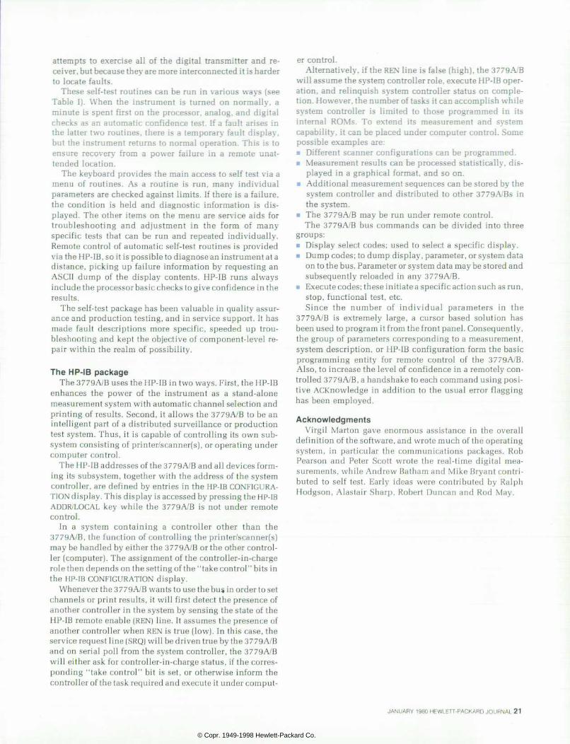
attempts to exercise all of the digital transmitter and re ceiver, but because they are more interconnected it is harder to locate faults.
These self-test routines can be run in various ways (see Table I). When the instrument is turned on normally, a minute is spent first on the processor, analog, and digital checks as an automatic confidence test. If a fault arises in the latter two routines, there is a temporary fault display, but the instrument returns to normal operation. This is to ensure recovery from a power failure in a remote unat tended location.
The keyboard provides the main access to self test via a menu of routines. As a routine is run, many individual parameters are checked against limits. If there is a failure, the condition is held and diagnostic information is dis played. The other items on the menu are service aids for troubleshooting and adjustment in the form of many specific tests that can be run and repeated individually. Remote control of automatic self-test routines is provided via the HP-IB, so it is possible to diagnose an instrument at a distance, picking up failure information by requesting an ASCII dump of the display contents. HP-IB runs always include the processor basic checks to give confidence in the results.
The self-test package has been valuable in quality assur ance and production testing, and in service support. It has made fault descriptions more specific, speeded up trou bleshooting and kept the objective of component-level re pair within the realm of possibility.
The HP- IB package The 3779A/B uses the HP-IB in two ways. First, the HP-IB
enhances the power of the instrument as a stand-alone measurement system with automatic channel selection and printing of results. Second, it allows the 3779A/B to be an intelligent part of a distributed surveillance or production test system. Thus, it is capable of controlling its own sub system consisting of printer/scannerfs), or operating under computer control.
The HP-IB addresses of the 3779A/B and all devices form ing its subsystem, together with the address of the system controller, are defined by entries in the HP-IB CONFIGURA TION display. This display is accessed by pressing the HP-IB ADDR/LOCAL key while the 3779A/B is not under remote control.
In a system containing a controller other than the 3779A/B, the function of controlling the printer/scanner(s) may be handled by either the 3779A/B or the other control ler (computer). The assignment of the controller-in-charge role then depends on the setting of the "take control" bits in the HP-IB CONFIGURATION display.
Whenever the 3 779A/B wants to use the bus in order to set channels or print results, it will first detect the presence of another controller in the system by sensing the state of the HP-IB remote enable (REN) line. It assumes the presence of another controller when REN is true (low). In this case, the service request line (SRQ) will be driven true by the 3779A/B and on serial poll from the system controller, the 3779A/B will either ask for controller-in-charge status, if the corres ponding "take control" bit is set, or otherwise inform the controller of the task required and execute it under comput
er control. Alternatively, if the REN line is false (high), the 3779A/B
will assume the system controller role, execute HP-IB oper ation, and relinquish system controller status on comple tion. However, the number of tasks it can accomplish while system controller is limited to those programmed in its internal ROMs. To extend its measurement and system capability, it can be placed under computer control. Some possible examples are: • Different scanner configurations can be programmed. • Measurement results can be processed statistically, dis
played in a graphical format, and so on. • Additional measurement sequences can be stored by the
system controller and distributed to other 3779A/Bs in the system.
• The 3779A/B may be run under remote control. The 3779A/B bus commands can be divided into three
groups: • Display select codes; used to select a specific display. • Dump codes; to dump display, parameter, or system data
on to the bus. Parameter or system data may be stored and subsequently reloaded in any 3779A/B.
• Execute codes; these initiate a specific action such as run, stop, functional test, etc. Since the number of individual parameters in the
3779A/B is extremely large, a cursor based solution has been used to program it from the front panel. Consequently, the group of parameters corresponding to a measurement, system description, or HP-IB configuration form the basic programming entity for remote control of the 3779A/B. Also, to increase the level of confidence in a remotely con trolled 3779A/B, a handshake to each command using posi tive ACKnowledge in addition to the usual error flagging has been employed.
Acknowledgments Virgil Marton gave enormous assistance in the overall
definition of the software, and wrote much of the operating system, in particular the communications packages. Rob Pearson and Peter Scott wrote the real-time digital mea surements, while Andrew Batham and Mike Bryant contri buted to self test. Early ideas were contributed by Ralph Hodgson, Alastair Sharp, Robert Duncan and Rod May.
JANUARY 1980 HEWLETT-PACKARD JOURNAL 21
© Copr. 1949-1998 Hewlett-Packard Co.

Vector Impedance Analysis to 1000 MHz This new impedance ana lyzer measures four teen impedance parameters o f two- te rmina l components . I t 's fast , s tab le, accurate, and wide-range.
by Toshio Ichino. Hideo Ohkawara, and Nor iyuki Sugihara
RADIO FREQUENCY impedance measurements, traditionally made with manually balanced imped ance bridges, have more recently been made with
analog vector impedance meters, Q meters, and network analyzers. These have not always been satisfactory be cause of accuracy or dynamic range limitations. We wanted to develop an RF impedance meter that overcame the de ficiencies of conventional impedance meters and could be used as a system component covering the HF to UHF mea surement frequency range (1 MHz to 1000 MHz). The result, Model 4191 A RF Impedance Analyzer (Fig. 1), is an instru ment that is unparalleled in measurement speed, accuracy and impedance measurement range.
This new analyzer's capabilities depend heavily on its powerful microprocessor and arithmetic/logic unit. Mea sured data is digitally corrected according to stored calibra tion data and the corrected data is converted to the selected parameters and displayed. This built-in processing power makes it possible to maintain a friendly user interface while meeting today's exacting customer requirements. The analyzer can serve a wide variety of customer needs, includ ing semiconductor and electronic component evaluation, materials testing, and communications-related component measurement.
Probably the key feature of the 4191A is that it is not a
conventional impedance meter that measures only imped ance. It can display any form of impedance including in ductance, capacitance, resistance, reactance, conductance, dissipation factor, and so on. Its measurable-impedance range is 1 milliohm to 100,000 ohms in impedance or 1 microsiemens to 50 Siemens in admittance, wide enough for most applications.
Measured parameters can be displayed as Z ,|Y|,6,R, X, G, B, L, or C. Any measured parameter can also be dis played as a percent deviation from a reference set on the front panel or programmed over the HP Interface Bus (HP- IB). As in conventional LCR meters, series or parallel equi valent circuit selection is provided. This wide selection allows the user to choose the most suitable measurement for the particular device under test.
A second major feature is the analyzer's accurate fre quency settability. A frequency synthesizer generates the test signal, which remains phase-locked to an internal quartz reference oscillator. The frequency of the test signal can be varied in 100-Hz steps from 1 MHz to 1000 MHz. The 100-Hz test frequency resolution is useful for measure ments on high-Q devices such as quartz crystals. Frequency start, stop, step, and auto or manual sweep controls facili-
*Compat ib !e w i th ANSI / IEEE 488-1978.
F i g . 1 . M o d e l 4 1 9 1 R F I m p e d a n c e A n a l y z e r m e a s u r e s i m p e d ances f rom 1 mi l to 100 kCl at f re q u e n c i e s f r o m 1 t o 1 0 0 0 M H z . Measurements are accurate within 0 . 5 % t o 2 % o f r e a d i n g . T h e a n a l y z e r h a s f r e q u e n c y s w e e p c a p a b i l i t y , 4 V i - d i g i t r e s o l u t i o n , bu i l t - i n dc b i as w i t h sweep capa bil i ty, high stabil i ty, and a selection of versati le test f ixtures.
2 2 H E W L E T T - P A C K A R D J O U R N A L J A N U A R Y 1 9 8 0
© Copr. 1949-1998 Hewlett-Packard Co.

4 I 3 1 R V V C C - F & R - F C H R R R C T E R I S T I C C 1 6 0 9 1 R )
1 B 0 . B Â ¡ s 2 9 8 . 0 3 7 0 . 3 4 6 0 . 0 5 5 0 . B 5 4 0 . B 7 3 0 . B B 2 0 . Q
FREO. C MHz]
tate the measurement of component characteristics. A sweepable dc bias voltage, controllable in 10-millivolt
steps to ±40.00 volts, is also included. This feature permits a very accurate plot of semiconductor characteristics (C-V plot).
HP-IB capability is standard and is useful in quality as surance tests or automated testing. All front-panel settings are remotely programmable and the measured data can be transmitted over the bus for calculation or manipulation. This feature contributes to lowering the cost of measure ment and saving measurement time. With a desktop com puter on the HP-IB, complex measurement control, statisti cal data analysis, and production of graphic plots of the measured data are possible.
A built-in backup memory memorizes all the calibration
Fig. 2 . (a) Capac i tance and res is tance o f a varac tor d iode as func t ions of f requency, measured wi th the 4191 A Impedance Analyzer at two different bias voltages, (b) C-V c h a r a c t e r i s t i c s o f t h e v a r a c t o r d iode at two test f requencies.
data for error correction and all the measurement settings. This is an important convenience for making measure ments that are repeated daily. The analyzer can store up to two independent measurement setups. A memorized front-panel setup, including frequency and bias, can be recalled instantly by pressing the recall key.
In UHF impedance measurements, test fixture design is very important. Model 4191A offers a precision coax test fixture, a convenient spring-clip fixture for holding chip components, and a conventional Q-meter/R-X meter binding-post fixture. Transistor impedance measurements can also be done with a network analyzer fixture by extend ing the DUT port with an air line. For circuit probing, a needle-tip probe is available.
The optional analog output offers an inexpensive way to
JANUARY 1980 HEWLETT-PACKARD JOURNAL 23
© Copr. 1949-1998 Hewlett-Packard Co.
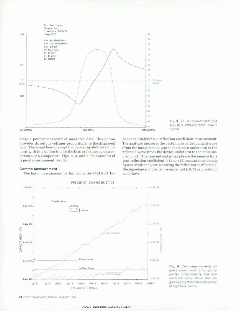
j '¿f
5th Oval — tone
Sampl. No. 1
Time/Dat» 8/20/79
Temp 23 'C
FS- 99. 99BB65Mhz
FP- 100. 0043B8MH
Co= 3. S2PF
R- 59. 47ohm
C- 0. 42FF
L- 6. 02mH
O- 63600
Fig . 3 . Z | -6 charac ter is t i cs o f a 1 0 0 - M H z f i f t h - o v e r t o n e q u a r t z crystal.
make a permanent record of measured data. This option provides dc output voltages proportional to the displayed data. The swept bias or swept frequency capabilities can be used with this option to plot the bias or frequency charac teristics of a component. Figs. 2,3, and 4 are examples of typical measurement results.
G a m m a M e a s u r e m e n t The basic measurement performed by the 4191A RF Im
pedance Analyzer is a reflection coefficient measurement. The analyzer measures the vector ratio of the incident wave (from the measurement port to the device under test) to the reflected wave (from the device under test to the measure ment port). The concept and principle are the same as for a port reflection coefficient (sll or s22) measurement made by a network analyzer. Knowing the reflection coefficient T, the impedance of the device under test (DUT) can be found as follows:
F R E Q U E N C Y C H A R A C T E R I S T I C S
•e lH 4. 0.-13
S a m p l e e l z e
G l a e e - E p o x y
e f 1 o n ~ E p a x y
. . 2 . 4 e - 0 5
< . . 1. 6e-05 Ã3
1 0 . B 1 0 0 0 . 0 2 0 B . 0 3 0 7 . 0 4 0 8 . 0 5 1 3 5 . 0 6 0 4 . 0 7 0 3 . 0 B 0 2 . 0 9 0 1 . 0 1 0 0 0 . 0
F R E Q U E N C Y C M H z ]
F i g . 4 . C - G m e a s u r e m e n t s o n g l a s s - e p o x y a n d t e f l o n - e p o x y p r i n t e d c i r c u i t b o a r d s . T h e c o n d u c t a n c e c u r v e s h o w s t h a t t h e g/ass-epoxy board becomes lossy at h igh f requencies.
2 4 H E W L E T T - P A C K A R D J O U R N A L J A N U A R Y 1 9 8 0
© Copr. 1949-1998 Hewlett-Packard Co.

Error Correction in the Impedance Analyzer
Systemat ic er rors in the 41 91 A RF Impedance Ana lyzer can be measured by cal ibrat ing the analyzer using the short, open, and 50(1 standards that are provided. Once these errors have been measured and stored, the analyzer automatical ly corrects measurements made on unknown dev ices under tes t (DUTs) .
I f we for F for the true ref lect ion coeff ic ient of the DUT and rm for the measured ref lect ion coef f ic ient o f the DUT, then:
Fm = en 0i r
where e^, e01 and e-, , are, respect ively, the direct iv i ty, t racking, and mismatch errors of the receiver sect ion.
I f we the rshor t for Fm of the shor t s tandard, ropen for rm of the open standard, and F0 for Fmof the 50Ã1 standard, then:
rShort = rm(r = -D=e00 -
ropen = rm (r = A) = eoo +
r0 = rm (r = o) = e00
(2)
(4)
where A is the ref lect ion coef f ic ient of the open standard. The open s t a n d a r d i s a s h i e l d e d o p e n t e r m i n a t i o n , a n d i t s c a p a c i t a n c e va lue in der i ved theore t i ca l l y . There a re th ree unknown fac to rs in equat ion 1 , and we have th ree equat ions (2 , 3 , and 4) , so we can solve for equat ion 1:
p = I m ( ^ s h o r t I o p e n ) "
I s h o r t ' ^ o p e n 0 + " ) * m C o p e n ~ * ~ " ^ s h o r t ) (5)
Open Capaci tance The open end of a coaxial l ine should look like an ideal open circuit,
but actually i t can be shown that the l ine is terminated in a capacit ive admi t tance because of the ef fect o f f r inge f ie lds and rad iat ion.
The 4191A's open-c i rcu i t s tandard is an open terminat ion cap or sh ie lded open . I t i s a sho r t cy l i nde r tha t ma tes w i th the tes t po r t connector , and i ts d iscont inui ty capaci tance is approximate ly 0.082 pF. The ref lect ion coeff ic ient of this capacitance is the factor A used in the error correct ion equat ion (5) .
Calibration Data Interpolation During calibration, the 41 91 A divides the frequency range entered
by the user into 50 equal or logarithmic intervals. The instrument takes ca l ibrat ion data at 51 points and s tores i t in i ts memory.
When the measurement f requency does not co inc ide wi th one o f the ca l ib ra t ion po in ts , the 4191 A in terpo la tes between ca l ib ra t ion points and carries out the error correction process. Since the simplest in terpo la t ion , a l inear approx imat ion , o f ten produces cons iderab le er ro r , a cub ic in te rpo la t ion is done us ing a Lagrange in te rpo la t ion formula . A cub ic curve that passes through four ca l ib ra t ion po in ts , two be fore the measurement f requency and two a f te r the measure men t f requency , i s genera ted . The va lue o f th i s cu rve a t the mea surement f requency is the va lue used for er ror correct ion.
Electr ical Length Compensat ion When is DUT is mounted at the end of a 50Ã1 transmission line that is
extended f rom the reference p lane of the 4191 A, the inc ident wave t ravels through the extended l ine f rom the test por t to the DUT. The ref lected wave travels through the l ine from the DUT to the test port. Assuming that the extended transmission l ine is a good 50Ã1 lossless l ine, the reflection coeff icient measured at the reference plane differs in phase by twice the e lectr ical length of the l ine f rom the t rue DUT ref lect ion coeff ic ient . I f the user enters the length of the l ine v ia the keyboa rd , t he 41 91 A compensa tes f o r t he phase sh i f t o f t he ex tended l ine. The compensat ing equat ion is :
Where Fm, Fshor t , and ropen are, respect ive ly , Fm - r0 , rshor t -To, and ropen - F0 .
The 4191A so lves equat ion 5 to der i ve the t rue re f lec t ion coe f f i c i en t o f t he DUT , t hen conve r t s t h i s va l ue t o t he r equ i r ed pa ram eters for d isplay.
. 2 , ,
T = rm e
Where Fm is F at the reference plane, I and c is the veloc i ty of l ight .
is the length of the extension,
Z = _ x 5 0 ( o h m s )
The selection of reflection coefficient as the basic mea surement mode provides the following advantages: 1. Easy remote control. A measurement is done and the
data processed digitally. There is no need to tune a variable air capacitor.
2. Extension of the DUT port with 50-ohm transmission line is possible.
3. Traceable impedance standards (Oil 50Ã1, OS) can be used for system calibration.
On the other hand, the measured DUT is not always close to 50 ohms. Generally speaking, measurement accuracy is poor for purely reactive components or those close to Oil and OS (short and open circuits).
To narrow the gap between its theoretical limits and its
actual performance, the 4191A had to be carefully de signed. To maintain a wide measurement range and accept able accuracy, severe requirements had to be placed on the test signal residual noise and the signal-to-noise ratio and accuracy of the RF-to-IF sampling frequency converter and receiver. To improve accuracy further, the measured data is error-corrected using prestored Oil, 50Ã1, and OS calibration data. In this way any residual error in the system is elimi nated. From this accurate reflection coefficient measure ment, further parameter conversion is done with stored programs. Thus impedance, admittance, capacitance, or inductance are easily determined.
RF Bridge The major sections of the impedance analyzer are the RF
bridge, the signal source, the receiver, and the digital SBC-
JANUARY 1980 HEWLETT-PACKARD JOURNAL 25
© Copr. 1949-1998 Hewlett-Packard Co.
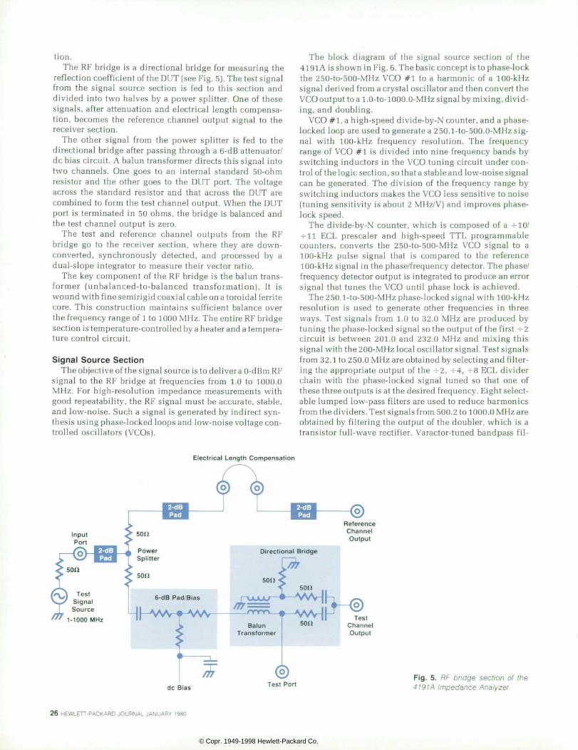
tion. The RF bridge is a directional bridge for measuring the
reflection coefficient of the DUT (see Fig. 5). The test signal from the signal source section is fed to this section and divided into two halves by a power splitter. One of these signals, after attenuation and electrical length compensa tion, becomes the reference channel output signal to the receiver section.
The other signal from the power splitter is fed to the directional bridge after passing through a 6-dB attenuator/ dc bias circuit. A balun transformer directs this signal into two channels. One goes to an internal standard 50-ohm resistor and the other goes to the DUT port. The voltage across the standard resistor and that across the DUT are combined to form the test channel output. When the DUT port is terminated in 50 ohms, the bridge is balanced and the test channel output is zero.
The test and reference channel outputs from the RF bridge go to the receiver section, where they are down- converted, synchronously detected, and processed by a dual-slope integrator to measure their vector ratio.
The key component of the RF bridge is the balun trans former (unbalanced-to-balanced transformation). It is wound with fine semirigid coaxial cable on a toroidal ferrite core. This construction maintains sufficient balance over the frequency range of 1 to 1000 MHz. The entire RF bridge section is temperature-controlled by a heater and a tempera ture control circuit.
Signal Source Sect ion The objective of the signal source is to deliver a 0-dBm RF
signal to the RF bridge at frequencies from 1.0 to 1000.0 MHz. For high-resolution impedance measurements with good repeatability, the RF signal must be accurate, stable, and low-noise. Such a signal is generated by indirect syn thesis using phase-locked loops and low-noise voltage con trolled oscillators (VCOs).
The block diagram of the signal source section of the 4191A is shown in Fig. 6. The basic concept is to phase-lock the 250-to-500-MHz VCO #1 to a harmonic of a 100-kHz signal derived from a crystal oscillator and then convert the VCO output to a l.O-to-1000. 0-MHz signal by mixing, divid ing, and doubling.
VCO #1, a high-speed divide-by-N counter, and a phase- locked loop are used to generate a 250. l-to-500. 0-MHz sig nal with 100-kHz frequency resolution. The frequency range of VCO #1 is divided into nine frequency bands by switching inductors in the VCO tuning circuit under con trol of the logic section, so that a stable and low-noise signal can be generated. The division of the frequency range by switching inductors makes the VCO less sensitive to noise (tuning sensitivity is about 2 MHz/V) and improves phase- lock speed.
The divide-by-N counter, which is composed of a -HlO/ -nil ECL prescaler and high-speed TTL programmable counters, converts the 250-to-500-MHz VCO signal to a 100-kHz pulse signal that is compared to the reference 100-kHz signal in the phase/frequency detector. The phase/ frequency detector output is integrated to produce an error signal that tunes the VCO until phase lock is achieved.
The 250.1-to-500-MHz phase-locked signal with 100-kHz resolution is used to generate other frequencies in three ways. Test signals from 1.0 to 32.0 MHz are produced by tuning the phase-locked signal so the output of the first n-2 circuit is between 201.0 and 232.0 MHz and mixing this signal with the 200-MHz local oscillator signal. Test signals from 32.1 to 250.0 MHz are obtained by selecting and filter ing the appropriate output of the n-2, n-4, n-8 ECL divider chain with the phase-locked signal tuned so that one of these three outputs is at the desired frequency. Eight select able lumped low-pass filters are used to reduce harmonics from the dividers. Test signals from 500.2 to 1000.0 MHz are obtained by filtering the output of the doubler, which is a transistor full-wave rectifier. Varactor-tuned bandpass fil-
Electr ical Length Compensat ion
Input Port
Reference Channel Output
Test Channel Output
dc Bias F i g . 5 . R F b r i d g e s e c t i o n o f t h e 4191 A Impedance Analyzer .
2 6 H E W L E T T - P A C K A R D J O U R N A L J A N U A R Y 1 9 8 0
© Copr. 1949-1998 Hewlett-Packard Co.

ters are used to reduce subharmonics caused by the doubler. Leveling of the output signal is achieved by feeding back
an ALC (automatic level control) signal to the PIN mod ulators in each frequency path. The ALC signal is an error voltage from the receiver section. Output power level at the test port is about -20 dBm ±1.5 dB from 1.0 MHz to 1.0 GHz. Test port power level variations are mainly the result of cable losses in the RF bridge and the conversion loss of the sampler in the receiver section.
Frequency resolution of 100 Hz (Option 002) is obtained by adding two more lock loops, a low-frequency synthe sizer loop and a summing loop. In 100-Hz frequency resolu tion operations, the 250-to-500-MHz VCO #1 is phase- locked to a harmonic of the 100-kHz reference to produce a signal between 249.1 and 499.0-MHz.
In the low-frequency synthesizer loop, the output signal of the 100-to- 11 0-MHz VCO, which is phase-locked to a harmonic of a 10-kHz reference, is divided by 100 to gener ate a low-noise 1.0000-to-l. 1000-MHz signal with 100-Hz frequency resolution. This signal is fed to the phase detec tor of a summing loop.
The 250-to-500-MHz VCO #2 is phase-locked such that the difference frequency of VCO #1 and VCO #2 is equal to the frequency of the low-frequency synthesizer loop, so the output frequency of VCO #2 is 250. 1000-to-500. 0000-MHz with 100-Hz frequency resolution.
The search generator, controlled by the frequency detec tor, is used to improve the phase-lock speed of the summing loop. It rapidly tunes VCO #2 towards the phase-lock fre quency. When the VCO #2 frequency is near the lock fre quency, the frequency detector stops the search generator and the loop is allowed to lock.
Receiver Section A block diagram of the receiver section is shown in Fig. 7.
The l.O-to-1000. 0-MHz RF signals from the RF bridge are down-converted to 100-kHz intermediate-frequency (IF) signals by a precision sampler and low-noise phase lock loop, the sampler acts l ike a harmonic mixer in a heterodyne frequency converter. After down-conversion the reference and test channel IF signals are synchronously detected and processed by the dual-slope integrator to mea sure their vector ratio.
The low-noise VCO, which covers a 60-to-90-MHz fre quency range in five bands, drives the programmable di vider, which divides the VCO frequency by a factor between 8 and 60. The 1.1-to-l 1.2 5-MHz square- wave signal from the programmable divider drives a step-recovery diode, which generates sampling pulses about 300 picoseconds wide.
Variations of the sampling efficiency of the samplers in both receiver channels are kept to a minimum by careful
100Hz Option
B P F = B a n d p a s s F i l t e r L P F = L o w - P a s s F i l t e r ALC = Automat ic Leve l Cont ro l VCO = Vol tage-Contro l led Osci l la tor
1.0-1000.0 MHz 0 dBm
100-MHz Crystal Oscillator 1.0-32.0 MHz
Fig. ind i rec t us ing s igna l source sect ion. Test s igna l is generated by ind i rec t synthes is us ing phase- locked loops and low-noise osc i l la tors .
J A N U A R Y 1 9 8 0 H E W L E T T - P A C K A R D J O U R N A L 2 7
© Copr. 1949-1998 Hewlett-Packard Co.
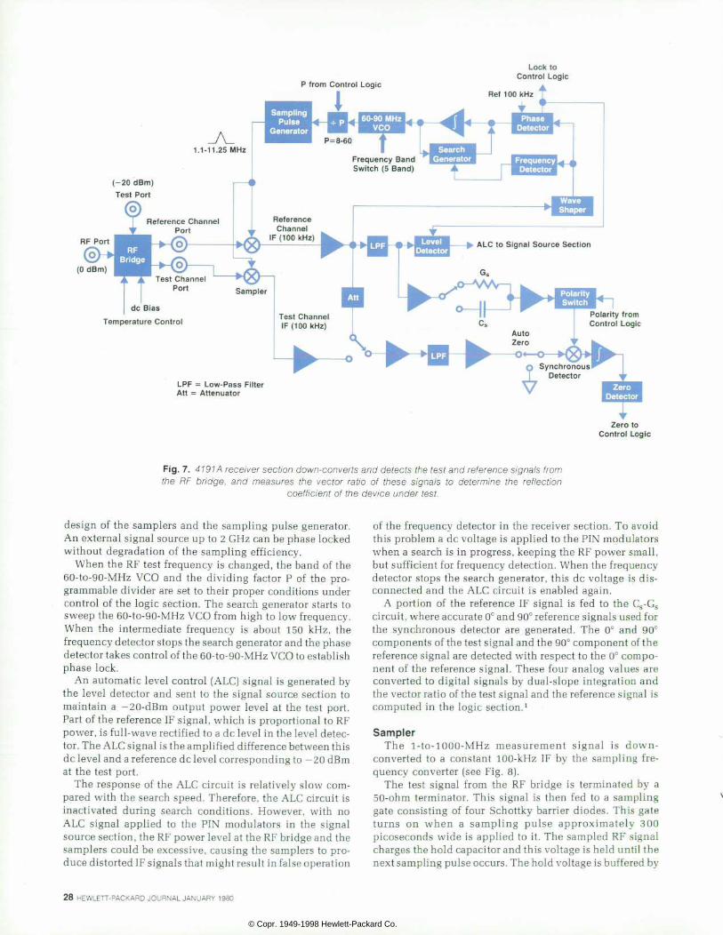
P from Control Logic
I
Lock to Control Logic
Ref 100 kHz
( - 2 0 d B m ) Test Port
Frequency Band Switch (5 Band)
^ ALC to Signal Source Sect ion
(0 dBm)
dc Bias Temperature Control
Polarity from Control Logic
LPF = Low-Pass Fi l ter Att = Attenuator
Q S y n c h r o n o u s ! Detector
V
Zero to Control Logic
Fig. test signals A receiver section down-converts and detects the test and reference signals from t h e R F b r i d g e , a n d m e a s u r e s t h e v e c t o r r a t i o o f t h e s e s i g n a l s t o d e t e r m i n e t h e r e f l e c t i o n
coef f ic ient of the device under test .
design of the samplers and the sampling pulse generator. An external signal source up to 2 GHz can be phase locked without degradation of the sampling efficiency.
When the RF test frequency is changed, the band of the 60-to-90-MHz VCO and the dividing factor P of the pro grammable divider are set to their proper conditions under control of the logic section. The search generator starts to sweep the 60-to-90-MHz VCO from high to low frequency. When the intermediate frequency is about 150 kHz, the frequency detector stops the search generator and the phase detector takes control of the 60-to-90-MHz VCO to establish phase lock.
An automatic level control (ALC) signal is generated by the level detector and sent to the signal source section to maintain a ^20-dBm output power level at the test port. Part of the reference IF signal, which is proportional to RF power, is full-wave rectified to a dc level in the level detec tor. The ALC signal is the amplified difference between this dc level and a reference dc level corresponding to - 20 dBm at the test port.
The response of the ALC circuit is relatively slow com pared with the search speed. Therefore, the ALC circuit is inactivated during search conditions. However, with no ALC signal applied to the PIN modulators in the signal source section, the RF power level at the RF bridge and the samplers could be excessive, causing the samplers to pro duce distorted IF signals that might result in false operation
of the frequency detector in the receiver section. To avoid this problem a dc voltage is applied to the PIN modulators when a search is in progress, keeping the RF power small, but sufficient for frequency detection. When the frequency detector stops the search generator, this dc voltage is dis connected and the ALC circuit is enabled again.
A portion of the reference IF signal is fed to the CS-GS circuit, where accurate 0° and 90° reference signals used for the synchronous detector are generated. The 0° and 90° components of the test signal and the 90° component of the reference signal are detected with respect to the 0° compo nent of the reference signal. These four analog values are converted to digital signals by dual-slope integration and the vector ratio of the test signal and the reference signal is computed in the logic section.1
Sampler The l-to-1000-MHz measurement signal is down-
converted to a constant 100-kHz IF by the sampling fre quency converter (see Fig. 8).
The test signal from the RF bridge is terminated by a 50-ohm terminator. This signal is then fed to a sampling gate consisting of four Schottky barrier diodes. This gate turns on when a sampling pulse approximately 300 picoseconds wide is applied to it. The sampled RF signal charges the hold capacitor and this voltage is held until the next sampling pulse occurs. The hold voltage is buffered by
2 8 H E W L E T T - P A C K A R D J O U R N A L J A N U A R Y 1 9 8 0
© Copr. 1949-1998 Hewlett-Packard Co.
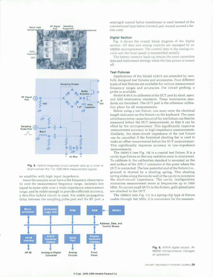
R F S i g n a l S a m p l i n g P o r t P u l s e P o r t
S a m p l i n g D i o d e s
- d c B i a s +
Fig . 8 . Hybr id - in tegra ted c i rcu i t sample r ac ts as a mixer to down-conver t the 1- to-WOO-MHz measurement s ignals .
an amplifier with high input impedance. Since the sampler must have a flat frequency characteris
tic over the measurement frequency range, maintain low signal-to-noise ratio over a wide impedance measurement range, and be stable enough to provide sufficient accuracy, a thin-film hybrid circuit is used. For stable propagation delay between the sampling pulse port and the RF port, a
semirigid coaxial balun transformer is used instead of the conventional type balun (twisted pair wound around a fer- rite core).
Digital Section Fig. 9 shows the overall block diagram of the digital
section. All data and analog controls are managed by an M6800 microprocessor. The control data to the analog cir cuits and the front panel is transmitted serially.
The battery memory back-up retains the error correction data and instrument settings when the line power is turned off.
Test Fixtures Applications of the Model 4191A are extended by care
fully designed test fixtures and accessories. Four different types of test fixtures are available for various measurement frequency ranges and accuracies. For circuit probing, a probe is available.
Model 4191 A is calibrated at the DUT port by short, open, and 50Ã1 termination standards. These termination stan dards are furnished. The DUT port is the reference calibra tion plane for all measurements.
Before using a test fixture, one must enter the electrical length indicated on the fixture via the keyboard. The open admittance (stray capacitance) of the test fixture can then be measured before the DUT measurement, so that it can be offset by the microprocessor. This significantly improves measurement accuracy in high-impedance measurements. Similarly, the short-circuit impedance of the test fixture can be cancelled if the furnished shorting bar is used to make an offset measurement before the DUT measurement. This significantly improves accuracy in low-impedance measurements.
The 16091A (see Fig. 10) is a coaxial test fixture. It is a cavity type fixture so that any radiation error is minimized. To calibrate it, the calibration standard is mounted on the end surface of the APC-7 connector at the point where the DUT is connected. The low-potential end of the fixture (i.e., ground) is shorted by a shorting spring. This shorting spring slides along the inside wall of the cavity to minimize the short-circuit impedance. The cavity configuration minimizes measurement errors at frequencies up to 1000 MHz. To mount small DUTs in the fixture, gold-plated pins are attached to the DUT.
The 16092A (see Fig. 11) is a spring-clip type of fixture usable through 500 MHz. It is convenient for the measure-
M i c r o processor
HP-IB In te r face
t HP-IB
Arithmetic/ Logic Unit
A-to-D Converter
Control
Analog-to-Digital Converter
Analog Circuits
Address, Data, and Control Buses
Display/ Keyboard Interface
I Fron t Panel
Fig . 9 . 4191 A d ig i ta l sec t ion . An M6800 m ic rop rocesso r manages al l operat ions.
JANUARY 1980 HEWLETT-PACKARD JOURNAL 29
© Copr. 1949-1998 Hewlett-Packard Co.

Parameter Conversion T h e 4 1 9 1 A R F I m p e d a n c e A n a l y z e r f u n d a m e n t a l l y m e a s u r e s t h e p . B _ p
r e f l e c t i o n c o e f f i c i e n t o f t h e d e v i c e u n d e r t e s t ( D U T ) a n d t h e n c o n v e r t s 2 7 r f F t h i s a d m i t i n t o o t h e r p a r a m e t e r s , s u c h a s i m p e d a n c e , a d m i t t a n c e , m a y a n d c a p a c i t a n c e . T h e c o n v e r s i o n e q u a t i o n s m a y 1 be summar ized as fo l lows (Z0 = 50 ohms) :
I m p e d a n c e 5 0 x - â € ” - = R Dissipat ion factor
Admi t tance
V R 2 + X 2 = | Z |
X = a r g Z = 6
tan = a r g Y = 6
Qual i ty factor
[Bl
w = D
= Q
The d iag ram shows se r ies and pa ra l l e l equ iva len t c i r cu i t s fo r t he DUT.
I n d u c t a n c e â € ” . = L s
ment of small chip capacitors or axial-lead components. The DUT is mounted by pressing the spring, inserting the DUT, and releasing the spring. This fixture is particularly convenient when minimum dielectric loss in the insulator and low series loss are desirable.
The 16093A and 16093B (see Fig. 12) are conventional binding post test fixtures similar to those used with R-X and
Q meters. These are useful up to 250 MHz or 125 MHz, respectively.
The 16094A (see Fig. 13) is a probe fixture that is mounted at the tip of a precision coaxial cable. It is useful for measuring impedance in circuits up to 125 MHz.
The extension capability of the DUT port is another im portant feature of Model 4191A. Measurement of the
' ^ *
Vert ical Section
Fig. 10. 76097 A coaxial f ixture set c o n s i s t s o f c a v i t y - t y p e f i x t u r e s useful up to WOO MHz.
3 0 H E W L E T T - P A C K A R D J O U R N A L J A N U A R Y 1 9 8 0
© Copr. 1949-1998 Hewlett-Packard Co.
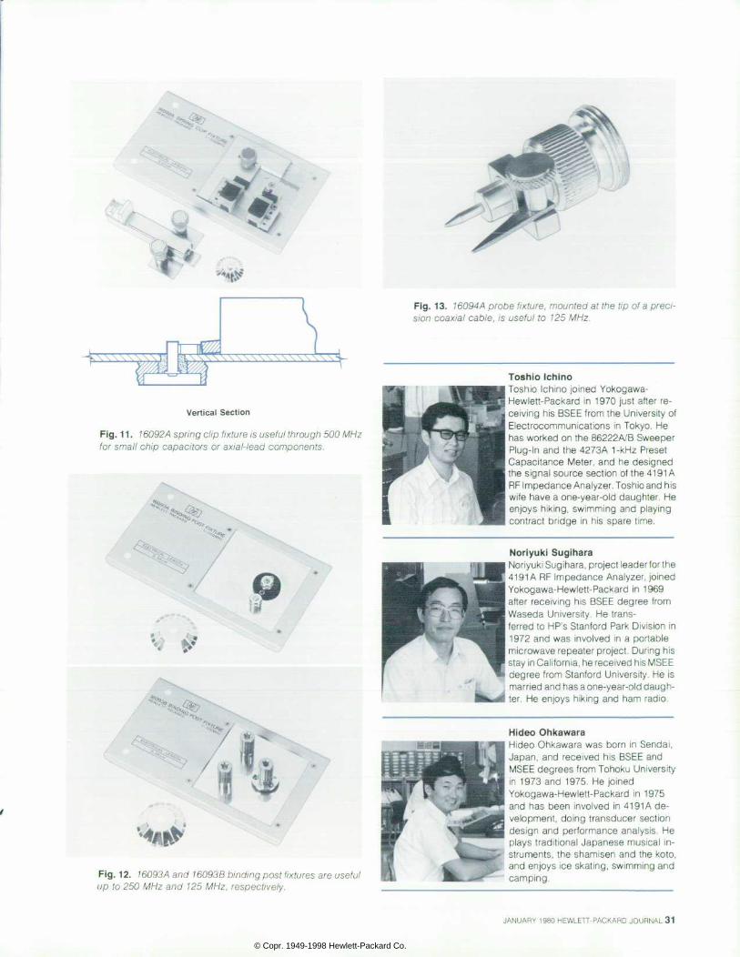
•
*
Vertical Section
Fig. 1 1 . J 6092/\ spring cl ip f ixture is useful through 500 MHz for smal l ch ip capac i tors or ax ia l - lead components .
fv*
Fig. 12. 16093A and 16093B b ind ing post f ix tures are usefu l up to 250 MHz and 125 MHz, respec t i ve ly .
F ig . 13. 16094 A probe f ix ture, mounted at the t ip o f a prec i s ion coaxia l cable, is usefu l to 125 MHz.
Toshio Ichino Tosh io Ich ino jo ined Yokogawa- Hewle t t -Packard in 1970 jus t a f te r re ceiving his BSEE from the Universi ty of E lec t rocommunicat ions in Tokyo. He has worked on the 86222A/B Sweeper P lug- In and the 4273A 1-kHz Preset Capac i tance Mete r , and he des igned the signal source sect ion of the 4191 A RF Impedance Analyzer. Toshio and his wi fe have a one-year-o ld daughter . He en joys h ik ing , swimming and p lay ing cont ract br idge in h is spare t ime.
Noriyuki Sugihara NoriyukiSugihara, project leader for the 41 91 A RF Impedance Analyzer, joined Yokogawa-Hewlet t -Packard in 1969 af ter receiv ing h is BSEE degree f rom Waseda Un ive rs i t y . He t rans ferred to HP's Stanford Park Division in 1972 and was invo lved in a por tab le microwave repeater project . Dur ing his stay in California, he received his MSEE degree f rom Stanford Universi ty. He is marr ied and has a one-year-o ld daugh ter . He en joys h ik ing and ham rad io .
Hideo Ohkawara Hideo Ohkawara was born in Senda i , Japan, and rece ived h is BSEE and MSEE degrees f rom Tohoku Univers i ty in 1973 and 1975. He jo ined Yokogawa-Hewle t t -Packard in 1975 and has been invo lved in 41 91 A de ve lopment , do ing t ransducer sec t ion des ign and per fo rmance ana lys is . He p lays t rad i t iona l Japanese mus ica l in s t ruments, the shamisen and the koto, and enjoys ice skat ing, swimming and camping.
JANUARY 1980 HEWLETT-PACKARD JOURNAL 31
© Copr. 1949-1998 Hewlett-Packard Co.

S P E C I F I C A T I O N S HP Model 41 91 A RF Impedance Analyzer
P A R A M E T E R S M E A S U R E D : | Z | - 6 , | Y | - 9 , | r | ( r e f l e c t i o n c o e f f i c i e n t ) - e , R - X , G - B , r x -Py ( rec tangu la r coo rd ina te d i sp lay o f I " ) , L -R -G-D Q , C -R G D-Q. DISPLAY: 4 ' /2-d ig i t max. , max. d isp lay 19999 count .
D E V I A T I O N M E A S U R E M E N T : D i s p l a y s m e a s u r e d v a l u e d e v i a t i o n ( A ) f r o m s t o r e d reference, or dev iat ion in percent (A%) for a l l parameters.
MEASURING SIGNAL: In te rna l Syn thes ize r : F R E Q U E N C Y R A N G E : 1 M H z t o 1 0 0 0 M H z FREQUENCY STEPS: 100 kHz (1 to 500 MHz) , 200 kHz (500 to 1000 MHz) FREQUENCY ACCURACY: ±3 ppm SIGNAL LEVEL ( te rminated w i th 50Ã! ) : -20±3 dBm
M E A S U R E M E N T M O D E : SPOT MEASUREMENT: Measures spec i f i c f requency (o r b ias vo l tage) . S W E E P M E A S U R E M E N T : L i n e a r s w e e p m e a s u r e m e n t o r l o g a r i t h m i c s w e e p m e a s u r e
ments. AUTOCALIBRATION: Automat ic er ror compensat ion re ferenced to connected terminat ion.
REFERENCE TERMINATIONS: O i l , 50O, OS. CALIBRATION FREQUENCIES: 51 f requenc ies be tween s ta r t and s top f requenc ies .
NOTE: Frequency error correction for other than calibration -frequencies is automatically done by thi rd-degree interpolat ion. Automat ical ly compensates for open capaci tance of 0.082 pF with OS terminat ion.
E L E C T R I C A L L E N G T H C O M P E N S A T I O N : A u t o m a t i c c o m p e n s a t i o n f o r e l e c t r i c a l length 0 to 99.99cm.
DC BIAS: In te rna l dc B ias : V O L T A G E R A N G E : - 4 0 . 0 0 V t o + 4 0 . 0 0 V , 1 0 m V s t e p s . SETTING ACCURACY: ±(0 .1% o f se t t i ng + 10 mV) .
KEY STATUS MEMORY: Measu remen t cond i t i ons se t by f r on t pane l keys can be s to red and recal led.
MEASURING TERMINAL: APC-7 connector . H P - I B D A T A O U T P U T A N D R E M O T E C O N T R O L : F u r n i s h e d . M E A S U R I N G R E S O L U T I O N A N D A C C U R A C Y :
F M E A S U R E M E N T : O.OOOOK
|r|, rx, ry RESOLUTION: 0.0001 | f | , r x , f y T Y P I C A L A C C U R A C I E S : 0 . 0 0 1 1 + 0 . 0 0 0 0 0 4 7 f 0 A C C U R A C Y : ( 0 . 0 0 3 5 + 0 . 0 0 0 0 1 f ) / | r | ( r a d . ) O MAX. RESOLUTION: 0.01° where f - measu r ing f requency i n MHz
MEASURING T IME: < 800 ms . < 250 ms i n H igh -Speed Mode . SIGNAL SETTLING TIME (when f requency is changed) : «200 ms.
General Information OPERATING TEMPERATURE: 0 to 55 'C, Re la t ive Humid i ty : <95% at 40°C. POWER: 100 , 120 , 220V ± 10%, 240V + 10% -5%, 48 to 66 Hz . POWER CONSUMPTION: 150VA max . D IMENSIONS: Approx . 425 .5 mm W x 230 mm H x 574 mm D. WEIGHT: Approx . 24 kg (s tandard mode l ) . A C C E S S O R Y F U R N I S H E D : A c c e s s o r y C a s e ( w i t h R e f e r e n c e T e r m i n a t i o n s O ! ! , 5 0 à 1
and OS). OPTIONS
OPTION 002: Internal Synthesizer in 100/20(1 Hz steps. OPTION 004: Recorder Output .
A C C E S S O R I E S A V A I L A B L E : 16091A COAXIAL F IXTURE SET: Measur ing f requency : 1 MHz to 1000 MHz. 16092A SPRING CLIP F IXTURE: Measur ing f requency : 1 to 500 MHz. 16093A Measur ing POST FIXTURE: Dis tance between posts : approx. 7 mm. Measur ing
f requency: 1 to 250 MHz. 1 6 0 9 3 B m m . P O S T F I X T U R E : D i s t a n c e b e t w e e n p o s t s : a p p r o x . 1 5 m m o r 1 8 m m .
Recommended measur ing f requency: 1 to 125 MHz. 16094A PROBE FIXTURE: Measur ing f requency : 1 to 125 MHz.
PRICES $445. U.S.A.: 4191A, $14,260. Option 002, $1680. Option 004, $445. MANUFACTURING D IV IS ION: Yokogawa-Hew le t t -Packa rd L td .
9-1, Takakura-cho, Hachio j i -shi Tokyo, Japan, 192
input/output impedance of a transistor is easily done using this capability. The DUT port is extended with a coaxial airline and attached to the HP 11600B/116002B Transistor Fixture. Calibration is done at the input of the transistor fixture. Another practical but important application is temperature tests. By extending the DUT port with a preci sion APC-7 coaxial airline, the temperature characteristics of a DUT mounted in an oven may be taken. Maximum extendable length depends upon the measurement fre quency and accuracy needed, but generally up to 1 m exten sion (approximately) is possible without significant degra dation of the measurement accuracy.
Acknowledgments Without the involvement and the efforts of many people,
this project could not have been successful. Team members who deserve special recognition are: Yukio Minami and Mitsuki Gotoh for analog circuit design, Jinichi Ikemoto and Takashi Yoshida for the digital section, Hiroshi Shiratori and Takashi Saitoh for mechanical design, Tsuneji Nakayasu for industrial design and test fixtures, and Hiroshi Sakayori for the hybrid sampler. Hitoshi Noguchi provided the framework. Special thanks are due to Masahide Nishida for his general management and encour agement.
Reference 1. K. Maeda and Y. Narimatsu, "Multi-Frequency LCR Meters Test Components under Realistic Conditions", Hewlett-Packard Journal, February 1979.
Hewlet t -Packard Company, 1501 Page Mi l l Road, Palo A l to , Cal i forn ia 94304
HEWLETT-PACKARD JOURNAL
Bulk Rate U.S. Postage
Paid Hewlet t -Packard
Company
JANUARY 1980 Volume 31 • Number 1 T e c h n i c a l I n f o r m a t i o n f r o m t h e L a b o r a t o r i e s o f
H e w l e t t - P a c k a r d C o m p a n y Hewle t t -Packard Company , 1501 Page Mi l l Road
Pa lo A l to , Ca l i f o rn ia 94304 USA Hewle t t -Packard Cent ra l Ma i l ing Depar tment
Van Heuven Goedhar t laan 121 1180 AM Ams te l veen The Ne the r l ands
Yokogawa-Hewle t t -Packard L td . , Sug inami -Ku Tokyo 1 68 Japan
0200 0106 10£Ã»t>BLAC£LCAOO H R C A t . L A C K B U R N J O H N H O P K I N S U N I V . A P P L l f c D P H Y S I C S L A B J O H N S H O P K I N S L A U R E L H P Z 0 8 I O
/ " ^ I a d d r e s s A n a m e I l i s t l a b e l . s ~ \ p " A | ~ " \ l ~ " N | ~ " ) F " " O ^ ^ . T o c h a n g e y o u r a d d r e s s o r d e l e t e y o u r n a m e f r o m o u r m a i l i n g l i s t p l e a s e s e n d u s y o u r o l d a d d r e s s l a b e l . S e n d U M A N b i L U r A U U n t o o . c h changes t o Hew le t t -Packa rd Jou rna l , 1501 Page M i l l Road , Pa lo A l t o . Ca l i f o rn i a 94304 U .S .A . A l l ow 60 days .
© Copr. 1949-1998 Hewlett-Packard Co.


![SK9822 REV.01 EN [兼容模张] · 2016. 3. 18. · 3/ 12 SK9822 SK9822: The default is RGB chips with IC integration 6. General Information](https://static.fdocuments.us/doc/165x107/60c8dd7214333e138a661027/sk9822-rev01-en-fafff-2016-3-18.jpg)