IT66121FN Datasheet v0 · 2013-10-16 · sck/mclk ws i2s0 i2s1 i2s2 i2s3/spdif vsync hsync ovdd 62...
39
www.ite.com.tw Nov-2011 Rev:0.99 1/39 IT66121FN Low Power Transmitter with HDMI1.4 3D Preliminary Datasheet Specification V0.99 ITE TECH. INC. Provide by Promaster彥陽科技
Transcript of IT66121FN Datasheet v0 · 2013-10-16 · sck/mclk ws i2s0 i2s1 i2s2 i2s3/spdif vsync hsync ovdd 62...
www.ite.com.tw
Nov-2011 Rev:0.99 1/39
IT66121FN
Low Power Transmitter with HDMI1.4 3D
Preliminary Datasheet
Specification V0.99
ITE TECH. INC.
Provid
e by P
romast
er彥陽
科技

IT66121FN
www.ite.com.tw
Nov-2011 Rev:0.99 2/39
General Description
The IT66121 is a high-performance and low-power single channel HDMI transmitter, fully compliant
with HDMI 1.3a, HDCP 1.2 and backward compatible to DVI 1.0 specifications. IT66121 also provide
the HDMI1.4 3D feature, which enables direct 3D displays through an HDMI link. The IT66121 serves
to provide the most cost-effective HDMI solution for DTV-ready consumer electronics such as set-top
boxes, DVD players and A/V receivers, as well as DTV-enriched PC products such as notebooks and
desktops, without compromising the performance. Its backward compatibility to DVI standard allows
connectivity to myriad video displays such as LCD and CRT monitors, in addition to the
ever-so-flourishing Flat Panel TVs.
Aside from the various video output formats supported, the IT66121 also supports 8 channels of I2S
digital audio, with sampling rate up to 192kHz and sample size up to 24 bits. IT66121 also support
S/PDIF input of up to 192kHz sampling rate.
The newly supported High-Bit Rate (HBR) audio by HDMI Specifications v1.3 is provided by the
IT66121 in two interfaces: with the four I2S input ports or the S/PDIF input port. With both interfaces
the highest possible HBR frame rate is supported at up to 768kHz
By default the IT66121 comes with integrated HDCP ROMs which are pre-programmed with HDCP
keys that ensures secure digital content transmission. Users need not worry about the procurement
and maintenance of the HDCP keys.
The IT66121 also provides a complete solution of Consumer Electronics Control (CEC) function. This
optional CEC feature of HDMI specification allows the user to control two or more CEC-enabled
devices through HDMI network. With IT66121 embedded CEC PHY, user can use high-level software
API to easily implement all the necessary remote control commands. The CEC bus related protocol is
handled by the CEC PHY which eliminates extra loading of the MCU.
Features
Single channel HDMI transmitter
Compliant with HDMI 1.3a, HDCP 1.2 and DVI 1.0 specifications
Supporting pixel rates from 25MHz to 165MHz
DTV resolutions: 480i, 576i, 480p, 576p, 720p, 1080i up to 1080p
PC resolutions: VGA, SVGA, XGA, SXGA up to UXGA
Various video input interface supporting digital video standards such as:
24-bit RGB/YCbCr 4:4:4 with RB swap option
Provid
e by P
romast
er彥陽
科技

IT66121FN
www.ite.com.tw
Nov-2011 Rev:0.99 3/39
16/20/24-bit YCbCr 4:2:2 with YC swap option
8/10/12-bit YCbCr 4:2:2 (CCIR-656)
BTA-T1004 format
DE-only interface
DDR option
Support HDMI1.4 3D feature
Frame packing mode up to [email protected]/24Hz and [email protected]/60Hz
Top and Bottom up to [email protected]/60Hz
Side-by-Side (Half) up to [email protected]/60Hz
Side-by-Side (Full) up to [email protected]/60Hz
Bi-direction Color Space Conversion (CSC) between RGB and YCbCr color spaces with
programmable coefficients.
Digital audio input interface supporting
audio sample rate: 32~192 kHz
sample size: 16~24 bits
four I2S interfaces supporting 8-channel audio
S/PDIF interface supporting PCM, Dolby Digital, DTS digital audio transmission at up to
192kHz
Support for high-bit-rate (HBR) audio such as DTS-HD and Dolby TrueHD through the four I2S
interface or the S/PDIF interface, with frame rates as high as 768kHz
Compatible with IEC 60958 and IEC 61937
Software programmable HDMI output current, enabling user to optimize the performance for
fixed-cable systems or those with pre-defined cable length
MCLK input is optional for audio operation. Users could opt to implement audio input interface with
or without MCLK.
Integrated pre-programmed HDCP keys
Purely hardware HDCP engine increasing the robustness and security of HDCP operation
Monitor detection through Hot Plug Detection and Receiver Termination Detection
Embedded full-function pattern generator
Intelligent, programmable power management
Embedded hardware controlled CEC PHY
Ultra low power consumption, operation power is less than 70mw at 1080p@60Hz format.
64-pin (9x9 mm) QFN package Pro
vide b
y Pro
master彥
陽科
技

IT66121FN
www.ite.com.tw
Nov-2011 Rev:0.99 4/39
Pin Diagram
IT66121FNQFN-64 9x9
(Top View)
31
D13
D12
D11
D10
D9
PCLK
D8
D7
D6
D5
IVDD12
D4
D3
D2
D1
D0
DE
32
33
35
41
40
39
38
37
36
34
44
43
42
PCADR
SYSRSTN
PCSDA
PCSCL
IVDD12
OVDD
D23
D22
D21
D20
D19
D18
D17
D16
D15
D14
OVDD33
16
45
46
48
47
49 5755 565453525150 605958
17
CEC
14
13
15
12
2
3
4
5
6
7
11
8
1
63 64
DDCSCL
DDCSDA
HPD
INT
IVDD12
VCC33
SCK/MCLK
WS
I2S0
I2S1
I2S2
I2S3/SPDIF
VSYNC
HSYNC
OVDD62
ENTEST
10
9
61
1819
PVCC12
PVCC33
2930 28 21222324252627 20TX2P
TX2M
DVDD12
TX1P
TX1M
TX0P
TX0M
AVCC12
TXCP
TXCM
REXT
PIN65: GND PAD
Figure 1. IT66121FN pin diagram
Provid
e by P
romast
er彥陽
科技

IT66121FN
www.ite.com.tw
Nov-2011 Rev:0.99 5/39
Pin Description
Digital Video Input Pins
Pin Name Direction Description Type Pin No.
D[23:0] Input Digital video input pins. LVTTL 36-50,
52-55,
57-61
DE Input Data enable LVTTL 62
HSYNC Input Horizontal sync. signal LVTTL 63
VSYNC Input Vertical sync. signal LVTTL 64
PCLK Input Input data clock LVTTL 51
Digital Audio Input Pins
Pin Name Direction Description Type Pin No.
SCK/MCLK Input I2S serial clock input /SPDIF master clock input LVTTL 7
WS Input I2S word select input LVTTL 6
I2S0 Input I2S 0 serial data input LVTTL 5
I2S1 Input I2S 1 serial data input LVTTL 4
I2S2 Input I2S 2 serial data input LVTTL 3
I2S3/SPDIF Input I2S 3 serial data input /SPDIF audio input LVTTL 2
HDMI Interface Pins
Pin Name Direction Description Type Pin No.
CEC I/O CEC signal (5V-tolerant) Schmitt 17
DDCSCL I/O I2C Clock for DDC (5V-tolerant) Schmitt 16
DDCSDA I/O I2C Data for DDC (5V-tolerant) Schmitt 15
HPD Input Hot Plug Detection (5V-tolerant) LVTTL 14
TMDS front-end interface pins
Pin Name Direction Description Type Pin No.
TX2P Analog HDMI Channel 2 positive output TMDS 30
TX2M Analog HDMI Channel 2 negative output TMDS 29
TX1P Analog HDMI Channel 1 positive output TMDS 27
TX1M Analog HDMI Channel 1 negative output TMDS 26
TX0P Analog HDMI Channel 0 positive output TMDS 25
TX0M Analog HDMI Channel 0 negative output TMDS 24
TXCP Analog HDMI Clock Channel positive output TMDS 22
Provid
e by P
romast
er彥陽
科技

IT66121FN
www.ite.com.tw
Nov-2011 Rev:0.99 6/39
TXCM Analog HDMI Clock Channel negative output TMDS 21
REXT Analog External resistor for setting TMDS output level. Default tied to
AGND via a 4.7K-Ohm SMD resistor.
Analog 20
Programming Pins
Pin Name Direction Description Type Pin No.
PCSCL Input Serial Programming Clock for chip programming (5V-tolerant) Schmitt 12
PCSDA I/O Serial Programming Data for chip programming (5V-tolerant) Schmitt 11
INT# Output Interrupt output. Default active-low (5V-tolerant) LVTTL 10
System Control Pins
Pin Name Direction Description Type Pin No.
ENTEST Input Must be tied low via a resistor. LVTTL 31
PCADR Input Serial programming device address select LVTTL 32
SYSRSTN Input Hardware reset pin. Active LOW Schmitt 33
Power/Ground Pins
Pin Name Description Type Pin No.
IVDD12 Digital logic power (1.2V) Power 8, 35, 56
OVDD I/O Pin power (1.8V or 2.5V or 3.3V) Power 1, 34
OVDD33 5V-tolerant I/O power (3.3V) Power 13
VCC33 Internal ROM power (3.3V) Power 9
PVCC12 HDMI core PLL power (1.2V) Power 18
PVCC33 HDMI core PLL power (3.3V) Power 19
AVCC12 HDMI analog frontend power (1.2V) Power 23
DVDD12 HDMI digital frontend power (1.2V) Power 28
GND Exposed ground pad Ground 65
Provid
e by P
romast
er彥陽
科技

IT66121FN
www.ite.com.tw
Nov-2011 Rev:0.99 7/39
Functional Description
IT66121 is a low-power version of HDMI 1.3 transmitter and provides complete solutions for HDMI
Source systems by implementing all the required HDMI functions. In addition, advanced processing
algorithms are employed to optimize the performance of video processing such as color space
conversion and YCbCr up/down-sampling. The following picture is the functional block diagram of
IT66121, which describes clearly the data flow.
Video Data Capture&DE GeneratorAudio Data CaptureColor Space Conversion4:2:24:4:4Pixel Repeat HDCP Cipher&Encryption Enginer TMDS Transmitter(DVI/HDMI)
I2C Master(to HDCP EEPROM) I2C Master(HDCP Controller)I2C Slave(to host)ConfigurationRegister BlocksPCLKVSYNCHSYNCDED[23:0]WSI2S3/SPDIF
PCADR DDCSCLDDCSDASCK/MCLK
PCSCL PCSDA ROMSCL ROMSDATX2P/MTX1P/MTX0P/MTXCP/MInterrupt Controller HPDINT
SYSRSTNCEC
PHYCEC
I2S0I2S1I2S2
Figure 2. Functional block diagram of IT66121
Video Data Processing Flow
Figure 3 depicts the video data processing flow. For the purpose of retaining maximum flexibility, most
of the block enabling and path bypassing are controlled through register programming. Please refer to
IT66121 Programming Guide for detailed and precise descriptions.
As can be seen from Figure 3, the first step of video data processing is to prepare the video data
(Data), data enable signal (DE), video clock (Clock), horizontal sync and vertical sync signals
(H/VSYNC). While the video data and video clock are always readily available from input pins, the
preparation of the data enable and sync signals require special extraction process (Embedded Ctrl.
Signals Extraction & DE Generator) depending on the format of input video data.
All the data then undergo a series of video processing including color-space conversion and YCbCr
Provid
e by P
romast
er彥陽
科技

IT66121FN
www.ite.com.tw
Nov-2011 Rev:0.99 8/39
up/down-sampling. Depending on the selected input and output video formats, different processing
blocks are either enabled or bypassed via register control. For the sake of flexibility, this is all done in
software register programming. Therefore, extra care should be taken in keeping the selected
input-output format combination and the corresponding video processing block selection. Please refer
to the IT66121 Programming Guide for suggested register setting.
Figure 3. Video data processing flow of IT66121
Designated as D[23:0], the input video data could take on bus width of 8 bits to 24 bits. This input
interface could be configured through register setting to provide various data formats as listed in Table
1.
Although not explicitly depicted in Figure 3, input video clock (PCLK) can be configured to be
multiplied by 0.5, 1, 2 or 4, so as to support special formats such as CCIR-656 and pixel-repeating.
This is also enabled by software programming.
General description of block functions is as follows:
Extraction of embedded control signals (Embedded Ctrl. Signals Extraction)
Input video formats with only embedded sync signals rely on this block to derive the proper Hsync,
Vsync and DE signals. Specifically, CCIR-656 video stream includes Start of Active Video (SAV) and
Provid
e by P
romast
er彥陽
科技

IT66121FN
www.ite.com.tw
Nov-2011 Rev:0.99 9/39
End of Active Video (EAV) that this block uses to extract the required control signals.
Generation of data enable signal (DE Generator)
DE signal defines the region of active video data. In cases where the video decoders supply no such
DE signals to IT66121, this block is used to generate appropriate DE signal from Hsync, Vsync and
Clock.
Upsampling (YCbCr422 to YCbCr444)
In cases where input signals are in YCbCr 4:2:2 format and output is selected as 4:4:4, this block is
enabled to do the upsampling.
Bi-directional Color Space Conversion (YCbCr ↔↔↔↔ RGB)
Many video decoders only offer YCbCr outputs, while DVI 1.0 supports only RGB color space. In order
to offer full compatibility between various Source and Sink combination, this block offers bi-directional
RGB ↔ YCbCr color space conversion (CSC). To provide maximum flexibility, the matrix coefficients
of the CSC engine in IT66121 are fully programmable. Users of IT66121 could elect to employ their
preferred conversion formula.
Downsampling (YCbCr444 to YCbCr422)
In cases where input signals are in YCbCr 4:4:4 format and output is selected as YCbCr 4:2:2, this
block is enabled to do the downsampling.
HDCP engine (HDCP)
The HDCP engine in IT66121 handles all the processing required by HDCP mechanism in hardware.
Software intervention is not necessary except checking for revocation. Preprogrammed HDCP keys
are also embedded in IT66121. Users need not worry about the purchasing and management of the
HDCP keys.
TMDS driver (TMDS Driver)
The final stop of the data processing flow is TMDS serializer. The TMDS driver serializes the input
parallel data and drive out the proper electrical signals to the HDMI cable. The output current level is
controlled through connecting a precision resistor of proper value to Pin 20 (REXT).
Provid
e by P
romast
er彥陽
科技

IT66121FN
www.ite.com.tw
Nov-2011 Rev:0.99 10/39
Supported Input Video Formats
Table 1 lists the input video formats supported by IT66121.
Input Pixel clock frequency (MHz)
Color
Space
Video
Format
Bus
Width
DDR/
SDR
Hsync/
Vsync 480i 480p XGA 720p 1080i SXGA 1080p UXGA
RGB 4:4:4
24 SDR Separate 13.5 27 65 74.25 74.25 108 148.5 162
12 DDR Separate 13.5 27 65 74.25 74.25
24 DDR Separate 13.5 32.5 37.125 37.125 54 74.25 81
YCbCr
4:4:4
24 SDR Separate 13.5 27 65 74.25 74.25 108 148.5 162
12 DDR Separate 13.5 27 65 74.25 74.25
24 DDR Separate 13.5 32.5 37.125 37.125 54 74.25 81
4:2:2
16/20/24 SDR Separate 13.5 27 65 74.25 74.25 108 148.5 162
Embedded 13.5 27 65 74.25 74.25 108 148.5 162
16/20/24 DDR Separate 13.5 32.5 37.125 37.125 54 74.25 81
Embedded 13.5 32.5 37.125 37.125 54 74.25 81
8/10/12 SDR Separate 27 54 130 148.5 148.5
Embedded 27 54 130 148.5 148.5
8/10/12 DDR Separate 13.5 27 65 74.25 74.25
Embedded 13.5 27 65 74.25 74.25
Table 1. Input video formats supported by IT66121 Notes: 1. Table cells that are left blanks are those format combinations that are not supported by IT66121. 2. Embedded sync signals are defined by CCIR-656 standard, using SAV/EAV sequences of FF, 00, 00, XY. 3. The original pixel clock of 480i is 13.5MHz. HDMI standard mandates that a 27MHz pixel clock be used and pixel
repeating is employed to keep the frequency range of the HDMI link within control.
Audio Data Capture and Processing
IT66121 takes in four I2S inputs as well as one S/PDIF input of audio data. The four I2S inputs allow
transmission of 8-channel uncompressed audio data at up to 192kHz sample rate. The S/PDIF input
allows transmission of uncompressed PCM data (IEC 60958) or compressed multi-channel data (IEC
61937) at up to 192kHz.
Note that MCLK input is optional for the IT66121. By default IT66121 generates the MCLK internally to
process the audio. Neither I2S nor S/PDIF inputs requires external MCLK signal. However, if the jitter
or the duty cycle of the input S/PDIF is considerable, coherent external MCLK input is recommended
and such configuration could be enabled through register setting. Refer to IT66121 Programming
Guide for such setting.
Provid
e by P
romast
er彥陽
科技

IT66121FN
www.ite.com.tw
Nov-2011 Rev:0.99 11/39
High-Bit-Rate (HBR) Audio is first introduced in the HDMI 1.3 standard. It is called upon by high-end
audio system such as DTS-HD and Dolby TrueHD. No specific interface is defined by the HBR
standard. The IT66121 supports HBR audio in two ways. One is to employ the four I2S inputs
simultaneously, where the original streaming HBR audio is broken into four parallel data streams
before entering the IT66121. The other is to use the S/PDIF input port. Since the data rate here is as
high as 98.304Mbps, a coherent MCLK is required in this application.
Interrupt Generation
The system micro-controller should take in the interrupt signal output by IT66121 at PIN 10 (INT). INT
pin can be configured as Push-pull or Tristate mode depending on user’s application. IT66121
generates an interrupt signal with events involving the following signals or situations:
1. Hot-plug detection (Pin 14, HPD) experiences state changes.
2. Receiver detection circuit reports the presence or absence of an active termination at the TMDS
Clock Channel (RxSENDetect)
3. DDC bus is hanged for any reasons
4. Audio FIFO overflows
5. HDCP authentication fails
6. Audio/Video data is stable or not
A typical initialization of HDMI link should be based on interrupt signal and appropriate register probing.
Recommended flow is detailed in IT66121 Programming Guide. Simply put, the microcontroller should
monitor the HPD status first. Upon valid HPD event, move on to check RxSENDetect register to see if
the receiver chip is ready for further handshaking. When RxSENDetect is asserted, start reading EDID
data through DDC channels and carry on the rest of the handshaking subsequently.
If the micro-controller makes no use of the interrupt signal as well as the above-mentioned status
registers, the link establishment might fail. Please do follow the suggested initialization flow
recommended in IT66121 Programming Guide.
Provid
e by P
romast
er彥陽
科技

IT66121FN
www.ite.com.tw
Nov-2011 Rev:0.99 12/39
Configuration and Function Control
IT66121 includes two serial programming ports by default (i.e. with embedded HDCP keys): one for
interfacing with micro-controller, the other for accessing the DDC channels of HDMI link.
The serial programming interface for interfacing the micro-controller is a slave interface, comprising
PCSCL (Pin 12) and PCSDA (Pin 11). The micro-controller uses this interface to monitor all the
statuses and control all the functions. Two device addresses are available, depending on the input
logic level of PCADR (Pin 32). If PCADR is pulled high by the user, the device address is 0x9A. If
pulled low, 0x98.
The I2C interface for accessing the DDC channels of the HDMI link is a master interface, comprising
DDCSCL (Pin 16) and DDCSDA (Pin 15). IT66121 uses this interface to read the EDID data and
perform HDCP authentication protocol with the sink device over the HDMI cable.
For temporarily storing the acquired EDID data, IT66121 includes a 32 bytes dedicated FIFO. The
micro-controller may command IT66121 to acquire 32 bytes of EDID information, read it back and then
continue to read the next 32 bytes until getting all necessary EDID information.
The HDCP protocol of IT66121 is completely implemented in hardware. No software intervention is
needed except for revocation list checking. Various HDCP-related statuses are stored in HDCP
registers for the reference of micro-controller. Refer to IT66121 Programming Guide for detailed
register descriptions. The HDCP Standard also specifies a special message read protocol other than
the standard I2C protocol. See Figure 4 for checking HDCP port link integrity.
Slave Addr (7)S R A Read Data (8) A Read Data (8) A Read Data (8) NA P
S=Start; R=Read; A=Ack; NA=No Ack; P=Stop
Figure 4. HDCP port link integrity message read
All serial programming interfaces conform to standard I2C transactions and operate at up to 100kHz.
Provid
e by P
romast
er彥陽
科技
IT66121FN
www.ite.com.tw
Nov-2011 Rev:0.99 13/39
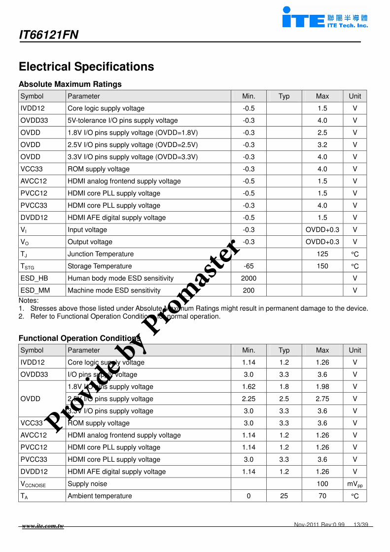
Electrical Specifications
Absolute Maximum Ratings
Symbol Parameter Min. Typ Max Unit
IVDD12 Core logic supply voltage -0.5 1.5 V
OVDD33 5V-tolerance I/O pins supply voltage -0.3 4.0 V
OVDD 1.8V I/O pins supply voltage (OVDD=1.8V) -0.3 2.5 V
OVDD 2.5V I/O pins supply voltage (OVDD=2.5V) -0.3 3.2 V
OVDD 3.3V I/O pins supply voltage (OVDD=3.3V) -0.3 4.0 V
VCC33 ROM supply voltage -0.3 4.0 V
AVCC12 HDMI analog frontend supply voltage -0.5 1.5 V
PVCC12 HDMI core PLL supply voltage -0.5 1.5 V
PVCC33 HDMI core PLL supply voltage -0.3 4.0 V
DVDD12 HDMI AFE digital supply voltage -0.5 1.5 V
VI Input voltage -0.3 OVDD+0.3 V
VO Output voltage -0.3 OVDD+0.3 V
TJ Junction Temperature 125 °C
TSTG Storage Temperature -65 150 °C
ESD_HB Human body mode ESD sensitivity 2000 V
ESD_MM Machine mode ESD sensitivity 200 V
Notes: 1. Stresses above those listed under Absolute Maximum Ratings might result in permanent damage to the device. 2. Refer to Functional Operation Conditions for normal operation.
Functional Operation Conditions
Symbol Parameter Min. Typ Max Unit
IVDD12 Core logic supply voltage 1.14 1.2 1.26 V
OVDD33 I/O pins supply voltage 3.0 3.3 3.6 V
OVDD
1.8V I/O pins supply voltage 1.62 1.8 1.98 V
2.5V I/O pins supply voltage 2.25 2.5 2.75 V
3.3V I/O pins supply voltage 3.0 3.3 3.6 V
VCC33 ROM supply voltage 3.0 3.3 3.6 V
AVCC12 HDMI analog frontend supply voltage 1.14 1.2 1.26 V
PVCC12 HDMI core PLL supply voltage 1.14 1.2 1.26 V
PVCC33 HDMI core PLL supply voltage 3.0 3.3 3.6 V
DVDD12 HDMI AFE digital supply voltage 1.14 1.2 1.26 V
VCCNOISE Supply noise 100 mVpp
TA Ambient temperature 0 25 70 °C
Provid
e by P
romast
er彥陽
科技

IT66121FN
www.ite.com.tw
Nov-2011 Rev:0.99 14/39
Θja Junction to ambient thermal resistance 40 °C/W
Notes: 1. AVCC12, PVCC12 and PVCC33 should be regulated. 2. See System Design Consideration for supply decoupling and regulation.
Provid
e by P
romast
er彥陽
科技

IT66121FN
www.ite.com.tw
Nov-2011 Rev:0.99 15/39
DC Electrical Specification
Under functional operation conditions
For 1.8V OVDD For 2.5V OVDD For 3.3V OVDD Unit
Symbol Parameter Pin Type Min Typ Max Min Typ Max Min Typ Max
VIH Input low voltage1 LVTTL 0.6 0.7 0.8 V
VIL Input high voltage1 LVTTL 1.2 1.7 2.0 V
VT- Schmitt trigger negative
going threshold voltage1 Schmitt 0.63 0.75 0.94 1.06 1.22 1.39 V
VT+ Schmitt trigger positive
going threshold voltage1 Schmitt 1.05 1.14 1.35 1.48 1.70 1.92 V
VOL Output low voltage1 LVTTL 0.4 0.4 0.4 V
VOH Output high voltage1 LVTTL 1.4 2.1 2.9 V
IIN Input leakage current1 all -10 +10 -10 +10 -10 +10 µA
IOZ Tri-state output leakage
current1 all -10 +10 -10 +10 -10 +10 µA
IOL Serial programming
output sink current2 Schmitt 2.5 10 mA
Vswing TMDS output
single-ended swing3 TMDS 400 600 400 600 400 600 mV
IOFF Single-ended standby
output current3 TMDS 10 10 10 µA
Notes: 1. Guaranteed by I/O design. 2. The serial programming output ports are not real open-drain drivers. Sink current is guaranteed by I/O design
under the condition of driving the output pin with 0.2V. In a real serial programming environment, multiple devices and pull-up resistors could be present on the same bus, rendering the effective pull-up resistance much lower than that specified by the I2C Standard. When set at maximum current, the serial programming output ports of
IT66121 are capable of pulling down an effective pull-up resistance as low as 500Ω connected to 5V termination voltage to the standard I2C VIL. When experiencing insufficient low level problem, try setting the current level to higher than default. Refer to IT66121 Programming Guide for proper register setting.
3. Limits defined by HDMI standard
Audio AC Timing Specification
Under functional operation conditions
Symbol Parameter Conditions Min Typ Max Unit
FS_I2S I2S sample rate Up to 8 channels 32 192 kHz
FS_SPDIF S/PDIF sample rate 2 channels 32 192 kHz
Provid
e by P
romast
er彥陽
科技

IT66121FN
www.ite.com.tw
Nov-2011 Rev:0.99 16/39
Video AC Timing Specification
Under functional operation conditions
Symbol Parameter Conditions Min Typ Max Unit
Tpixel PCLK pixel clock period1 Single-edged
clocking
6.06 40 ns
Fpixel PCLK pixel clock frequency1 25 165 MHz
TCDE PCLK dual-edged clock period2 Dual-edged
clocking
13.47 40 ns
FCDE PCLK dual-edged clock frequency2 25 74.25 MHz
TPDUTY PCLK clock duty cycle 40% 60%
TPJ PCLK worst-case jitter 2.0 ns
TS Video data setup time3 Single-edged
clocking
1.5 ns
TH Video data hold time3 0.7 ns
TSDE Video data setup time3 Dual-edged
clocking
1.5 ns
THDE Video data hold time3 0.7 ns
Notes: 1. Fpixel is the inverse of Tpixel. Operating frequency range is given here while the actual video clock frequency
should comply with all video timing standards. Refer to Table 1 for supported video timings and corresponding pixel frequencies.
2. 12-bit dual-edged clocking is supported up to 74.5MHz of PCLK frequency, which covers 720p/1080i. 3. All setup time and hold time specifications are with respect to the latching edge of PCLK selected by the user
through register programming.
Provid
e by P
romast
er彥陽
科技

IT66121FN
www.ite.com.tw
Nov-2011 Rev:0.99 17/39
Operation Supply Current Specification
Normal Operation Mode
TYPICAL Mode TTL input test 3.3V, 2.5V and 1.8V
Resolution Mode HDCP
Video
In/Out
Format
Audio Deep Color Video Pattern
480P@60Hz
HDMI On YUV444 to
RGB444 48K2Ch 8bits
720P@60Hz
1080P@60Hz
1600x1200@60Hz DVI Off No CSC Off 8bits
MAX Mode TTL input test 3.3V, 2.5V and 1.8V
Resolution Mode HDCP
Video
In/Out
Format
Audio Deep Color Video Pattern
480P@60Hz
HDMI On YUV444to
RGB444 192K2Ch 8bits
720P@60Hz
1080P@60Hz
1600x1200@60Hz DVI Off No CSC Off 8bits
Symbol Video Timing PCLK(MHz) TYPICAL MAX Unit
IOVDD33
480P60 8-bit 27.0 0.07 0.07 mA
720P60 8-bit 74.25 0.07 0.07 mA
1080P60 8-bit 148.5 0.07 0.07 mA
1600x1200P60 8-bit 162.0 0.07 0.07 mA
IVCC33
480P60 8-bit 27.0 0.04 0.04 mA
720P60 8-bit 74.25 0.04 0.04 mA
1080P60 8-bit 148.5 0.04 0.04 mA
1600x1200P60 8-bit 162.0 0.00 0.00 mA
IPVCC33 480P60 8-bit 27.0 1.68 1.68 mA
Provid
e by P
romast
er彥陽
科技

IT66121FN
www.ite.com.tw
Nov-2011 Rev:0.99 18/39
720P60 8-bit 74.25 5.77 5.77 mA
1080P60 8-bit 148.5 3.16 3.16 mA
1600x1200P60 8-bit 162.0 3.53 3.53 mA
IIVDD12
480P60 8-bit 27.0 4.77 6.10 mA
720P60 8-bit 74.25 11.02 13.24 mA
1080P60 8-bit 148.5 21.22 24.63 mA
1600x1200P60 8-bit 162.0 16.745 20.6 mA
IDVDD12
480P60 8-bit 27.0 1.36 1.36 mA
720P60 8-bit 74.25 3.44 3.44 mA
1080P60 8-bit 148.5 6.69 6.69 mA
1600x1200P60 8-bit 162.0 7.2 7.2 mA
IAVCC12
480P60 8-bit 27.0 9.95 9.95 mA
720P60 8-bit 74.25 10.69 10.69 mA
1080P60 8-bit 148.5 11.84 11.84 mA
1600x1200P60 8-bit 162.0 12.0 12.0 mA
IPVCC12
480P60 8-bit 27.0 0.87 0.87 mA
720P60 8-bit 74.25 2.32 2.32 mA
1080P60 8-bit 148.5 2.6 2.6 mA
1600x1200P60 8-bit 162.0 2.85 2.85 mA
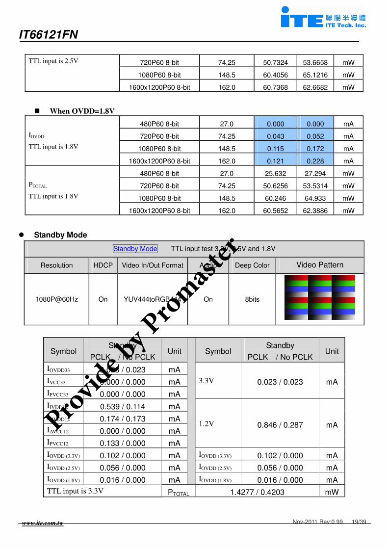
When OVDD=3.3V
IOVDD
TTL input is 3.3V
480P60 8-bit 27.0 0.13 0.15 mA
720P60 8-bit 74.25 0.3 0.37 mA
1080P60 8-bit 148.5 0.49 0.65 mA
1600x1200P60 8-bit 162.0 0.44 0.75 mA
PTOTAL
TTL input is 3.3V
480P60 8-bit 27.0 26.676 28.338 mW
720P60 8-bit 74.25 53.358 56.253 mW
1080P60 8-bit 148.5 63.228 68.848 mW
1600x1200P60 8-bit 162.0 63.84 65.535 mW
When OVDD=2.5V
IOVDD
TTL input is 2.5V
480P60 8-bit 27.0 0.036 0.065 mA
720P60 8-bit 74.25 0.132 0.164 mA
1080P60 8-bit 148.5 0.248 0.328 mA
1600x1200P60 8-bit 162.0 0.264 0.461 mA
PTOTAL 480P60 8-bit 27.0 25.6752 27.372 mW
Provid
e by P
romast
er彥陽
科技
IT66121FN
www.ite.com.tw
Nov-2011 Rev:0.99 19/39
TTL input is 2.5V 720P60 8-bit 74.25 50.7324 53.6658 mW
1080P60 8-bit 148.5 60.4056 65.1216 mW
1600x1200P60 8-bit 162.0 60.7368 62.6682 mW
When OVDD=1.8V
IOVDD
TTL input is 1.8V
480P60 8-bit 27.0 0.000 0.000 mA
720P60 8-bit 74.25 0.043 0.052 mA
1080P60 8-bit 148.5 0.115 0.172 mA
1600x1200P60 8-bit 162.0 0.121 0.228 mA
PTOTAL
TTL input is 1.8V
480P60 8-bit 27.0 25.632 27.294 mW
720P60 8-bit 74.25 50.6256 53.5314 mW
1080P60 8-bit 148.5 60.246 64.933 mW
1600x1200P60 8-bit 162.0 60.5652 62.3886 mW
Standby Mode
Standby Mode TTL input test 3.3V, 2.5V and 1.8V
Resolution HDCP Video In/Out Format Audio Deep Color Video Pattern
1080P@60Hz On YUV444toRGB444 On 8bits
Symbol Standby
PCLK / No PCLK Unit
Symbol Standby
PCLK / No PCLK Unit
IOVDD33 0.023 / 0.023 mA
3.3V 0.023 / 0.023 mA IVCC33 0.000 / 0.000 mA
IPVCC33 0.000 / 0.000 mA
IIVDD12 0.539 / 0.114 mA
1.2V 0.846 / 0.287 mA IDVDD12 0.174 / 0.173 mA
IAVCC12 0.000 / 0.000 mA
IPVCC12 0.133 / 0.000 mA
IOVDD (3.3V) 0.102 / 0.000 mA IOVDD (3.3V) 0.102 / 0.000 mA
IOVDD (2.5V) 0.056 / 0.000 mA IOVDD (2.5V) 0.056 / 0.000 mA
IOVDD (1.8V) 0.016 / 0.000 mA IOVDD (1.8V) 0.016 / 0.000 mA
TTL input is 3.3V PTOTAL 1.4277 / 0.4203 mW
Provid
e by P
romast
er彥陽
科技

IT66121FN
www.ite.com.tw
Nov-2011 Rev:0.99 20/39
TTL input is 2.5V PTOTAL 1.2311 / 0.4203 mW
TTL input is 1.8V PTOTAL 1.1199 / 0.4203 mW Notes:
1. PTOTAL are calculated by multiplying the supply currents with their corresponding supply voltage and summing up all the items.
Video Data Bus Mappings
IT66121 supports various input data mappings and formats, including those with embedded control
signals only. Corresponding register setting is mandatory for any chosen input data mappings. Refer
to IT66121 Programming Guide for detailed instruction.
Color Space Video Format Bus Width SDR/DDR H/Vsync Clocking Table Figure
RGB 4:4:4
24 SDR
Separate 1X
3 5
12 DDR 12 12
24 DDR 0.5X 13 13
YCbCr
4:4:4
24 SDR
Separate 1X
3 5
12 DDR 12 12
24 DDR 0.5X 13 13
4:2:2
16/20/24 SDR Separate
1X 4 6
Embedded 5 7
16/20/24 DDR Separate
0.5X 14 14
Embedded Note 1
8/10/12 SDR Separate
2X 8 10
Embedded 7 9
8/10/12 DDR Separate
1X Note 2
Embedded 15 15
Table 2. Input video format supported by IT66121 Notes: 1. The mapping of this format is the same as Table 5 and the timing diagram is similar to Figure 14 except the syncs
are embedded. 2. The mapping of this format is the same as Table 8 and the timing diagram is similar to Figure 15 except the syncs
are separated.
With certain input formats, not all 24 data input pins are used. In that case, it is recommended to tie the
unused input pins to ground. Pro
vide b
y Pro
master彥
陽科
技

IT66121FN
www.ite.com.tw
Nov-2011 Rev:0.99 21/39
24-bit RGB/YCbCr444 (Separate Syncs)
These are the simplest formats, with a complete definition of every pixel in each clock period. Timing
diagram is depicted in Fig.5.
Pin Name RGB YCbCr D0 B0 Cb0 D1 B1 Cb1 D2 B2 Cb2 D3 B3 Cb3 D4 B4 Cb4 D5 B5 Cb5 D6 B6 Cb6 D7 B7 Cb7 D8 G0 Y0 D9 G1 Y1
D10 G2 Y2 D11 G3 Y3 D12 G4 Y4 D13 G5 Y5 D14 G6 Y6 D15 G7 Y7 D16 R0 Cr0 D17 R1 Cr1 D18 R2 Cr2 D19 R3 Cr3 D20 R4 Cr4 D21 R5 Cr5 D22 R6 Cr6 D23 R7 Cr7
HSYNC HSYNC HSYNC VSYNC VSYNC VSYNC
DE DE DE
Table 3. Mappings of 24-bit RGB/YCbCr444 (separate syncs)
Figure 5. 24-bit RGB/YCbCr444 (separate syncs)
Provid
e by P
romast
er彥陽
科技

IT66121FN
www.ite.com.tw
Nov-2011 Rev:0.99 22/39
16/20/24-bit YCbCr422 with Separate Syncs
YCbCr 4:2:2 format does not have one complete pixel for every clock period. Luminace channel (Y) is
given for every pixel, while the two chroma channels are given alternatively on every other clock
period. The DE period should contain an even number of clock periods.
YCbCr 4:2:2 16-bit YCbCr 4:2:2 20-bit YCbCr 4:2:2 24-bit Pin Name Pixel#2N Pixel#2N+1 Pixel#2N Pixel#2N+1 Pixel#2N Pixel#2N+1
D0 grounded grounded grounded grounded Y0 Y0 D1 grounded grounded grounded grounded Y1 Y1 D2 grounded grounded Y0 Y0 Y2 Y2 D3 grounded grounded Y1 Y1 Y3 Y3 D4 Y0 Y0 Y2 Y2 Y4 Y4 D5 Y1 Y1 Y3 Y3 Y5 Y5 D6 Y2 Y2 Y4 Y4 Y6 Y6 D7 Y3 Y3 Y5 Y5 Y7 Y7 D8 Y4 Y4 Y6 Y6 Y8 Y8 D9 Y5 Y5 Y7 Y7 Y9 Y9
D10 Y6 Y6 Y8 Y8 Y10 Y10 D11 Y7 Y7 Y9 Y9 Y11 Y11 D12 grounded grounded grounded grounded Cb0 Cr0 D13 grounded grounded grounded grounded Cb1 Cr1 D14 grounded grounded Cb0 Cr0 Cb2 Cr2 D15 grounded grounded Cb1 Cr1 Cb3 Cr3 D16 Cb0 Cr0 Cb2 Cr2 Cb4 Cr4 D17 Cb1 Cr1 Cb3 Cr3 Cb5 Cr5 D18 Cb2 Cr2 Cb4 Cr4 Cb6 Cr6 D19 Cb3 Cr3 Cb5 Cr5 Cb7 Cr7 D20 Cb4 Cr4 Cb6 Cr6 Cb8 Cr8 D21 Cb5 Cr5 Cb7 Cr7 Cb9 Cr9 D22 Cb6 Cr6 Cb8 Cr8 Cb10 Cr10 D23 Cb7 Cr7 Cb9 Cr9 Cb11 Cr11
HSYNC HSYNC HSYNC HSYNC HSYNC HSYNC HSYNC VSYNC VSYNC VSYNC VSYNC VSYNC VSYNC VSYNC
DE DE DE DE DE DE DE
Table 4. Mappings of 16/20/24-bit YCbCr422 with separate syncs
Figure 6. 16/20/24-bit YCbCr422 with separate syncs
Provid
e by P
romast
er彥陽
科技

IT66121FN
www.ite.com.tw
Nov-2011 Rev:0.99 23/39
16/20/24-bit YCbCr422 with Embedded Syncs
This is similar to the previous format. The only difference is that the syncs are embedded. Bus width
could be 16-bit, 20-bit or 24-bit.
YCbCr 4:2:2 16-bit YCbCr 4:2:2 20-bit YCbCr 4:2:2 24-bit Pin Name Pixel#2N Pixel#2N+1 Pixel#2N Pixel#2N+1 Pixel#2N Pixel#2N+1
D0 grounded grounded grounded grounded Y0 Y0 D1 grounded grounded grounded grounded Y1 Y1 D2 grounded grounded Y0 Y0 Y2 Y2 D3 grounded grounded Y1 Y1 Y3 Y3 D4 Y0 Y0 Y2 Y2 Y4 Y4 D5 Y1 Y1 Y3 Y3 Y5 Y5 D6 Y2 Y2 Y4 Y4 Y6 Y6 D7 Y3 Y3 Y5 Y5 Y7 Y7 D8 Y4 Y4 Y6 Y6 Y8 Y8 D9 Y5 Y5 Y7 Y7 Y9 Y9
D10 Y6 Y6 Y8 Y8 Y10 Y10 D11 Y7 Y7 Y9 Y9 Y11 Y11 D12 grounded grounded grounded grounded Cb0 Cr0 D13 grounded grounded grounded grounded Cb1 Cr1 D14 grounded grounded Cb0 Cr0 Cb2 Cr2 D15 grounded grounded Cb1 Cr1 Cb3 Cr3 D16 Cb0 Cr0 Cb2 Cr2 Cb4 Cr4 D17 Cb1 Cr1 Cb3 Cr3 Cb5 Cr5 D18 Cb2 Cr2 Cb4 Cr4 Cb6 Cr6 D19 Cb3 Cr3 Cb5 Cr5 Cb7 Cr7 D20 Cb4 Cr4 Cb6 Cr6 Cb8 Cr8 D21 Cb5 Cr5 Cb7 Cr7 Cb9 Cr9 D22 Cb6 Cr6 Cb8 Cr8 Cb10 Cr10 D23 Cb7 Cr7 Cb9 Cr9 Cb11 Cr11
HSYNC grounded grounded grounded grounded grounded grounded VSYNC grounded grounded grounded grounded grounded grounded
DE grounded grounded grounded grounded grounded grounded
Table 5. Mappings of 16/20/24-bit YCbCr422 with embedded syncs
Figure 7. 16/20/24-bit YCbCr422 with embedded syncs
Provid
e by P
romast
er彥陽
科技

IT66121FN
www.ite.com.tw
Nov-2011 Rev:0.99 24/39
Note:
1. FF, 00, 00, XY information are mapped to D[11:4]
2. 20-bit mode is compatible with BT1120 format 20-bit mode
Provid
e by P
romast
er彥陽
科技

IT66121FN
www.ite.com.tw
Nov-2011 Rev:0.99 25/39
16/20/24-bit YCbCr422 with Embedded Syncs (BTA-T1004 Format)
The BTA-T1004 format is similar to the previous format except the SAV and EAV positions.
YCbCr 4:2:2 16-bit YCbCr 4:2:2 20-bit YCbCr 4:2:2 24-bit Pin Name Pixel#2N Pixel#2N+1 Pixel#2N Pixel#2N+1 Pixel#2N Pixel#2N+1
D0 grounded grounded grounded grounded Y0 Y0 D1 grounded grounded grounded grounded Y1 Y1 D2 grounded grounded Y0 Y0 Y2 Y2 D3 grounded grounded Y1 Y1 Y3 Y3 D4 Y0 Y0 Y2 Y2 Y4 Y4 D5 Y1 Y1 Y3 Y3 Y5 Y5 D6 Y2 Y2 Y4 Y4 Y6 Y6 D7 Y3 Y3 Y5 Y5 Y7 Y7 D8 Y4 Y4 Y6 Y6 Y8 Y8 D9 Y5 Y5 Y7 Y7 Y9 Y9
D10 Y6 Y6 Y8 Y8 Y10 Y10 D11 Y7 Y7 Y9 Y9 Y11 Y11 D12 grounded grounded grounded grounded Cb0 Cr0 D13 grounded grounded grounded grounded Cb1 Cr1 D14 grounded grounded Cb0 Cr0 Cb2 Cr2 D15 grounded grounded Cb1 Cr1 Cb3 Cr3 D16 Cb0 Cr0 Cb2 Cr2 Cb4 Cr4 D17 Cb1 Cr1 Cb3 Cr3 Cb5 Cr5 D18 Cb2 Cr2 Cb4 Cr4 Cb6 Cr6 D19 Cb3 Cr3 Cb5 Cr5 Cb7 Cr7 D20 Cb4 Cr4 Cb6 Cr6 Cb8 Cr8 D21 Cb5 Cr5 Cb7 Cr7 Cb9 Cr9 D22 Cb6 Cr6 Cb8 Cr8 Cb10 Cr10 D23 Cb7 Cr7 Cb9 Cr9 Cb11 Cr11
HSYNC grounded grounded grounded grounded grounded grounded VSYNC grounded grounded grounded grounded grounded grounded
DE grounded grounded grounded grounded grounded grounded
Table 6. Mappings of YCbCr422 with embedded syncs (BTA-T1004 format)
Figure 8. 16/20/24-bit YCbCr422 with embedded syncs (BTA-T1004 format)
Note:
1. FF, 00, 00, XY information are mapped to D[23:16] and D[11:4]
Provid
e by P
romast
er彥陽
科技

IT66121FN
www.ite.com.tw
Nov-2011 Rev:0.99 26/39
8/10/12-bit YCbCr422 with Embedded Syncs
This format is another variation of the YCbCr formats. The bus width is further reduced by half
compared from the previous YCbCr 4:2:2 formats, to either 8-bit, 10-bit or 12-bit. To compensate for
the halving of data bus, PCLK is doubled. With the double-rate input clock, luminance channel (Y) and
chroma channels (Cb or Cr) are alternated.
YCbCr 4:2:2 8-bit YCbCr 4:2:2 10-bit YCbCr 4:2:2 12-bit
Pin Name 1st PCLK 2nd PCLK 1st PCLK 2nd PCLK Pixel#2N Pixel#2N+1
D0 grounded grounded grounded grounded grounded grounded
D1 grounded grounded grounded grounded grounded grounded
D2 grounded grounded grounded grounded grounded grounded
D3 grounded grounded grounded grounded grounded grounded
D4 grounded grounded grounded grounded C0 Y0
D5 grounded grounded grounded grounded C1 Y1
D6 grounded grounded C0 Y0 C2 Y2
D7 grounded grounded C1 Y1 C3 Y3
D8 C0 Y0 C2 Y2 C4 Y4
D9 C1 Y1 C3 Y3 C5 Y5
D10 C2 Y2 C4 Y4 C6 Y6
D11 C3 Y3 C5 Y5 C7 Y7
D12 C4 Y4 C6 Y6 C8 Y9
D13 C5 Y5 C7 Y7 C9 Y9
D14 C6 Y6 C8 Y8 C10 Y10
D15 C7 Y7 C9 Y9 C11 Y11
D16 grounded grounded grounded grounded grounded grounded
D17 grounded grounded grounded grounded grounded grounded
D18 grounded grounded grounded grounded grounded grounded
D19 grounded grounded grounded grounded grounded grounded
D20 grounded grounded grounded grounded grounded grounded
D21 grounded grounded grounded grounded grounded grounded
D22 grounded grounded grounded grounded grounded grounded
D23 grounded grounded grounded grounded grounded grounded
HSYNC grounded grounded grounded grounded grounded grounded
VSYNC grounded grounded grounded grounded grounded grounded
DE grounded grounded grounded grounded grounded grounded
Table 7. Mappings of 8/10/12-bit YCbCr422 with embedded syncs
Provid
e by P
romast
er彥陽
科技

IT66121FN
www.ite.com.tw
Nov-2011 Rev:0.99 27/39
Figure 9. 8/10/12-bit YCbCr422 with embedded syncs
Note:
1. FF, 00, 00, XY information are mapped to D[15:8]
2. 8-bit mode is compatible with CCIR656 format
3. 10-bit mode is compatible with BT1120 format 10-bit mode
Provid
e by P
romast
er彥陽
科技

IT66121FN
www.ite.com.tw
Nov-2011 Rev:0.99 28/39
8/10/12-bit YCbCr422 with Separate Syncs
This format is simply the variation of previously mentioned one plus separate syncs.
YCbCr 4:2:2 8-bit YCbCr 4:2:2 10-bit YCbCr 4:2:2 12-bit
Pin Name 1st PCLK 2nd PCLK 1st PCLK 2nd PCLK Pixel#2N Pixel#2N+1 D0 grounded grounded grounded grounded grounded grounded
D1 grounded grounded grounded grounded grounded grounded
D2 grounded grounded grounded grounded grounded grounded
D3 grounded grounded grounded grounded grounded grounded
D4 grounded grounded grounded grounded C0 Y0
D5 grounded grounded grounded grounded C1 Y1
D6 grounded grounded C0 Y0 C2 Y2
D7 grounded grounded C1 Y1 C3 Y3
D8 C0 Y0 C2 Y2 C4 Y4
D9 C1 Y1 C3 Y3 C5 Y5
D10 C2 Y2 C4 Y4 C6 Y6
D11 C3 Y3 C5 Y5 C7 Y7
D12 C4 Y4 C6 Y6 C8 Y9
D13 C5 Y5 C7 Y7 C9 Y9
D14 C6 Y6 C8 Y8 C10 Y10
D15 C7 Y7 C9 Y9 C11 Y11
D16 grounded grounded grounded grounded grounded grounded D17 grounded grounded grounded grounded grounded grounded D18 grounded grounded grounded grounded grounded grounded D19 grounded grounded grounded grounded grounded grounded D20 grounded grounded grounded grounded grounded grounded D21 grounded grounded grounded grounded grounded grounded D22 grounded grounded grounded grounded grounded grounded D23 grounded grounded grounded grounded grounded grounded
HSYNC HSYNC HSYNC HSYNC VSYNC VSYNC VSYNC VSYNC
DE DE DE DE
Table 8. Mappings of 8/10/12-bit YCbCr422 with separate syncs
Figure 10. 8/10/12-bit YCbCr422 with separate syncs
Provid
e by P
romast
er彥陽
科技

IT66121FN
www.ite.com.tw
Nov-2011 Rev:0.99 29/39
The IT66121 supports another IO mapping method of YCbCr 4:2:2 formats which we call
Non-sequential IO Mode. The only difference between these two modes is the Y/Cb/Cr data mapping
sequence of the IO pin. The following tables show the different mappings of these two modes.
Non-sequential IO mode of 16/20/24-bit YCbCr422
YCbCr 4:2:2 16-bit YCbCr 4:2:2 20-bit YCbCr 4:2:2 24-bit Pin Name Pixel#2N Pixel#2N+1 Pixel#2N Pixel#2N+1 Pixel#2N Pixel#2N+1
D0 grounded grounded grounded grounded Y0 Y0 D1 grounded grounded grounded grounded Y1 Y1 D2 grounded grounded Y0 Y0 Y2 Y2 D3 grounded grounded Y1 Y1 Y3 Y3 D4 grounded grounded grounded grounded Cb0 Cr0 D5 grounded grounded grounded grounded Cb1 Cr1 D6 grounded grounded Cb0 Cr0 Cb2 Cr2 D7 grounded grounded Cb1 Cr1 Cb3 Cr3 D8 Y0 Y0 Y2 Y2 Y4 Y4 D9 Y1 Y1 Y3 Y3 Y5 Y5
D10 Y2 Y2 Y4 Y4 Y6 Y6 D11 Y3 Y3 Y5 Y5 Y7 Y7 D12 Y4 Y4 Y6 Y6 Y8 Y8 D13 Y5 Y5 Y7 Y7 Y9 Y9 D14 Y6 Y6 Y8 Y8 Y10 Y10 D15 Y7 Y7 Y9 Y9 Y11 Y11 D16 Cb0 Cr0 Cb2 Cr2 Cb4 Cr4 D17 Cb1 Cr1 Cb3 Cr3 Cb5 Cr5 D18 Cb2 Cr2 Cb4 Cr4 Cb6 Cr6 D19 Cb3 Cr3 Cb5 Cr5 Cb7 Cr7 D20 Cb4 Cr4 Cb6 Cr6 Cb8 Cr8 D21 Cb5 Cr5 Cb7 Cr7 Cb9 Cr9 D22 Cb6 Cr6 Cb8 Cr8 Cb10 Cr10 D23 Cb7 Cr7 Cb9 Cr9 Cb11 Cr11
HSYNC HSYNC HSYNC HSYNC HSYNC HSYNC HSYNC VSYNC VSYNC VSYNC VSYNC VSYNC VSYNC VSYNC
DE DE DE DE DE DE DE
Table 9. Mappings of 16/20/24-bit YCbCr422 non-sequential IO mode
Provid
e by P
romast
er彥陽
科技

IT66121FN
www.ite.com.tw
Nov-2011 Rev:0.99 30/39
Non-sequential IO mode of 8/10/12-bit YCbCr422 YCbCr 4:2:2 8-bit YCbCr 4:2:2 10-bit YCbCr 4:2:2 12-bit
Pin Name 1st PCLK 2nd PCLK 1st PCLK 2nd PCLK Pixel#2N Pixel#2N+1
D0 grounded grounded grounded grounded C0 Y0
D1 grounded grounded grounded grounded C1 Y1
D2 grounded grounded C0 Y0 C2 Y2
D3 grounded grounded C1 Y1 C3 Y3
D4 grounded grounded grounded grounded grounded grounded
D5 grounded grounded grounded grounded grounded grounded
D6 grounded grounded grounded grounded grounded grounded
D7 grounded grounded grounded grounded grounded grounded
D8 C0 Y0 C2 Y2 C4 Y4
D9 C1 Y1 C3 Y3 C5 Y5
D10 C2 Y2 C4 Y4 C6 Y6
D11 C3 Y3 C5 Y5 C7 Y7
D12 C4 Y4 C6 Y6 C8 Y9
D13 C5 Y5 C7 Y7 C9 Y9
D14 C6 Y6 C8 Y8 C10 Y10
D15 C7 Y7 C9 Y9 C11 Y11
D16 grounded grounded grounded grounded grounded grounded
D17 grounded grounded grounded grounded grounded grounded
D18 grounded grounded grounded grounded grounded grounded
D19 grounded grounded grounded grounded grounded grounded
D20 grounded grounded grounded grounded grounded grounded
D21 grounded grounded grounded grounded grounded grounded
D22 grounded grounded grounded grounded grounded grounded
D23 grounded grounded grounded grounded grounded grounded
HSYNC grounded grounded grounded grounded grounded grounded
VSYNC grounded grounded grounded grounded grounded grounded
DE grounded grounded grounded grounded grounded grounded
Table 10. Mappings of 8/10/12-bit YCbCr422 non-sequential IO mode
In additional to the previous input formats, there are three options can be supported by the IT66121.
DE-only option can be used for those input formats without H/VSync information. Dual-edge triggering
with half bus width option can be used to reduce the necessary bus width and dual-edge triggering
with half pixel clock option allows half input pixel clock. No all the input formats listed above can
support three options and please refer to the IT66121 programming guide for more information. Some
examples shown below are the corresponding timing relations when these options are enabled.
Provid
e by P
romast
er彥陽
科技

IT66121FN
www.ite.com.tw
Nov-2011 Rev:0.99 31/39
DE-Only Option: use 24-bit RGB/YCbCr444 (DE-only mode) as example
Pin Name RGB YCbCr D0 B0 Cb0 D1 B1 Cb1 D2 B2 Cb2 D3 B3 Cb3 D4 B4 Cb4 D5 B5 Cb5 D6 B6 Cb6 D7 B7 Cb7 D8 G0 Y0 D9 G1 Y1
D10 G2 Y2 D11 G3 Y3 D12 G4 Y4 D13 G5 Y5 D14 G6 Y6 D15 G7 Y7 D16 R0 Cr0 D17 R1 Cr1 D18 R2 Cr2 D19 R3 Cr3 D20 R4 Cr4 D21 R5 Cr5 D22 R6 Cr6 D23 R7 Cr7
HSYNC grounded grounded VSYNC grounded grounded
DE DE DE
Table 11. Mappings of 24-bit RGB/YCbCr444 (DE-only mode)
Figure 11. 24-bit RGB/YCbCr444 (DE-only mode)
Provid
e by P
romast
er彥陽
科技

IT66121FN
www.ite.com.tw
Nov-2011 Rev:0.99 32/39
Dual-Edge Triggering with Half Bus Width: use 12-bit RGB/YCbCr444 format as
example RGB YCbCr
Pin Name 1st edge 2nd edge 1st edge 2nd edge D0 B0 G4 Cb0 Y4 D1 B1 G5 Cb1 Y5 D2 B2 G6 Cb2 Y6 D3 B3 G7 Cb3 Y7 D4 B4 R0 Cb4 Cr0 D5 B5 R1 Cb5 Cr1 D6 B6 R2 Cb6 Cr2 D7 B7 R3 Cb7 Cr3 D8 G0 R4 Y0 Cr4 D9 G1 R5 Y1 Cr5
D10 G2 R6 Y2 Cr6 D11 G3 R7 Y3 Cr7 D12 grounded grounded grounded grounded D13 grounded grounded grounded grounded D14 grounded grounded grounded grounded D15 grounded grounded grounded grounded D16 grounded grounded grounded grounded D17 grounded grounded grounded grounded D18 grounded grounded grounded grounded D19 grounded grounded grounded grounded D20 grounded grounded grounded grounded D21 grounded grounded grounded grounded D22 grounded grounded grounded grounded D23 grounded grounded grounded grounded
HSYNC HSYNC HSYNC VSYNC VSYNC VSYNC
DE DE DE
Table 12. Mappings of 12-bit RGB/YCbCr444 dual-edge triggering (separate syncs)
D[23:12]
D[11:8]
PCLK
DE
H/VSYNC
D[7:4]
D[3:0]
Figure 12. 12-bit RGB/YCbCr444 dual-edge triggering (separate syncs)
Provid
e by P
romast
er彥陽
科技

IT66121FN
www.ite.com.tw
Nov-2011 Rev:0.99 33/39
Dual-Edge Triggering with Half Pixel Clock:
Example 1: 24-bit RGB/YCbCr444 with Separate Syncs and Dual-Edge Triggering
Pin Name RGB YCbCr
D0 B0 Cb0 D1 B1 Cb1 D2 B2 Cb2 D3 B3 Cb3 D4 B4 Cb4 D5 B5 Cb5 D6 B6 Cb6 D7 B7 Cb7 D8 G0 Y0 D9 G1 Y1
D10 G2 Y2 D11 G3 Y3 D12 G4 Y4 D13 G5 Y5 D14 G6 Y6 D15 G7 Y7 D16 R0 Cr0 D17 R1 Cr1 D18 R2 Cr2 D19 R3 Cr3 D20 R4 Cr4 D21 R5 Cr5 D22 R6 Cr6 D23 R7 Cr7
HSYNC HSYNC HSYNC VSYNC VSYNC VSYNC
DE DE DE
Table 13. Mappings of 24-bit RGB/YCbCr444 dual-edge triggering (separate syncs)
Figure 13. 24-bit RGB/YCbCr444 dual-edge triggering (separate syncs)
Provid
e by P
romast
er彥陽
科技

IT66121FN
www.ite.com.tw
Nov-2011 Rev:0.99 34/39
Example 2: 16/20/24-bit YCbCr422 with Separate Syncs using Dual-Edge Triggering
YCbCr 4:2:2 16-bit YCbCr 4:2:2 20-bit YCbCr 4:2:2 24-bit Pin Name 1st edge 2nd edge 1st edge 2nd edge 1st edge 2nd edge
D0 grounded grounded grounded grounded Y0 Y0 D1 grounded grounded grounded grounded Y1 Y1 D2 grounded grounded Y0 Y0 Y2 Y2 D3 grounded grounded Y1 Y1 Y3 Y3 D4 Y0 Y0 Y2 Y2 Y4 Y4 D5 Y1 Y1 Y3 Y3 Y5 Y5 D6 Y2 Y2 Y4 Y4 Y6 Y6 D7 Y3 Y3 Y5 Y5 Y7 Y7 D8 Y4 Y4 Y6 Y6 Y8 Y8 D9 Y5 Y5 Y7 Y7 Y9 Y9
D10 Y6 Y6 Y8 Y8 Y10 Y10 D11 Y7 Y7 Y9 Y9 Y11 Y11 D12 grounded grounded grounded grounded Cb0 Cr0 D13 grounded grounded grounded grounded Cb1 Cr1 D14 grounded grounded Cb0 Cr0 Cb2 Cr2 D15 grounded grounded Cb1 Cr1 Cb3 Cr3 D16 Cb0 Cr0 Cb2 Cr2 Cb4 Cr4 D17 Cb1 Cr1 Cb3 Cr3 Cb5 Cr5 D18 Cb2 Cr2 Cb4 Cr4 Cb6 Cr6 D19 Cb3 Cr3 Cb5 Cr5 Cb7 Cr7 D20 Cb4 Cr4 Cb6 Cr6 Cb8 Cr8 D21 Cb5 Cr5 Cb7 Cr7 Cb9 Cr9 D22 Cb6 Cr6 Cb8 Cr8 Cb10 Cr10 D23 Cb7 Cr7 Cb9 Cr9 Cb11 Cr11
HSYNC HSYNC HSYNC HSYNC HSYNC HSYNC HSYNC VSYNC VSYNC VSYNC VSYNC VSYNC VSYNC VSYNC
DE DE DE DE DE DE DE
Table 14. Mappings of 16/20/24-bit YCbCr422 dual-edge triggering (separate syncs)
Figure 14. 16/20/24-bit YCbCr422 dual-edge triggering (separate syncs)
Provid
e by P
romast
er彥陽
科技
IT66121FN
www.ite.com.tw
Nov-2011 Rev:0.99 35/39
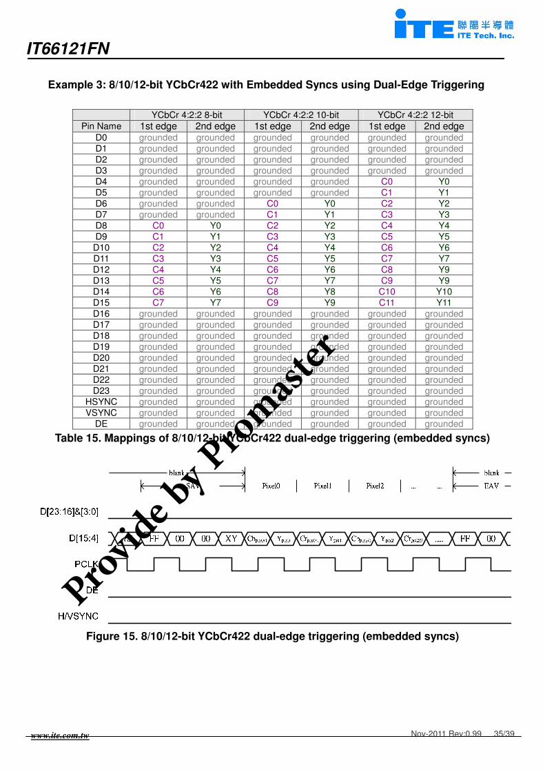
Example 3: 8/10/12-bit YCbCr422 with Embedded Syncs using Dual-Edge Triggering
YCbCr 4:2:2 8-bit YCbCr 4:2:2 10-bit YCbCr 4:2:2 12-bit
Pin Name 1st edge 2nd edge 1st edge 2nd edge 1st edge 2nd edge D0 grounded grounded grounded grounded grounded grounded
D1 grounded grounded grounded grounded grounded grounded
D2 grounded grounded grounded grounded grounded grounded
D3 grounded grounded grounded grounded grounded grounded
D4 grounded grounded grounded grounded C0 Y0
D5 grounded grounded grounded grounded C1 Y1
D6 grounded grounded C0 Y0 C2 Y2
D7 grounded grounded C1 Y1 C3 Y3
D8 C0 Y0 C2 Y2 C4 Y4
D9 C1 Y1 C3 Y3 C5 Y5
D10 C2 Y2 C4 Y4 C6 Y6
D11 C3 Y3 C5 Y5 C7 Y7
D12 C4 Y4 C6 Y6 C8 Y9
D13 C5 Y5 C7 Y7 C9 Y9
D14 C6 Y6 C8 Y8 C10 Y10
D15 C7 Y7 C9 Y9 C11 Y11
D16 grounded grounded grounded grounded grounded grounded
D17 grounded grounded grounded grounded grounded grounded
D18 grounded grounded grounded grounded grounded grounded
D19 grounded grounded grounded grounded grounded grounded
D20 grounded grounded grounded grounded grounded grounded
D21 grounded grounded grounded grounded grounded grounded
D22 grounded grounded grounded grounded grounded grounded
D23 grounded grounded grounded grounded grounded grounded
HSYNC grounded grounded grounded grounded grounded grounded
VSYNC grounded grounded grounded grounded grounded grounded
DE grounded grounded grounded grounded grounded grounded
Table 15. Mappings of 8/10/12-bit YCbCr422 dual-edge triggering (embedded syncs)
Figure 15. 8/10/12-bit YCbCr422 dual-edge triggering (embedded syncs)
Provid
e by P
romast
er彥陽
科技

IT66121FN
www.ite.com.tw
Nov-2011 Rev:0.99 36/39
System Design Consideration
As a high-performance receiver/transmitter, ITE’s RX/TX is capable of receiving/transmitting those
signals that are attenuated and degraded by the HDMI cables. These signals are usually very small in
amplitudes in addition to the distortion that the cable inflicts on them. The analog front-end of ITE’s
RX/TX is designed to combat environment noises as well as interference to some degree. However, to
get the optimum performance the system designers should follow the guideline below when designing
the application circuits and PCB layout.
HDMI Differential Signal
The characteristic impedance of all differential PCB traces (RX2P/M, RX1P/M, RX0P/M, and
RXCP/M) should be kept 100_ all the way from the HDMI connector to ITE’s RX/TX. This is very
crucial to the system performance at high speeds. When routing these 4 differential transmission
lines (8 single-ended lines in total), the following guidelines should be followed:
1. The signals traces should be on the outside layers (e.g. TOP layer) while beneath it there
should be a continuous ground plane in order to maintain the called micro-strip structure,
giving stable and well-defined characteristic impedances.
2. Cornering, through holes, crossing and any irregular signal routing should be avoided so as
to prevent from disrupting the EM field and creating discontinuity in characteristic impedance.
3. ITE’s RX/TX should be placed as close to the HDMI connector as possible. Since the TMDS
signal pins of ITE’s RX/TX perfectly match the order of the connector pins, it is very
convenient to route the signal directly into the chip, without through holes or angling.
4. Carefully choose the width and spacing of the differential transmission lines as their
characteristic impedance depends on various parameters of the PCB: trace width, trace
spacing, copper thickness, dielectric constant, dielectric thickness, etc. Careful 3D EM
simulation is the best way to derive a correct dimension that enables nominal 100_
differential impedance. Please contact us directly for technical support of this issue.
5. The sensitive HDMI differential signals should be taken when routing. To reduce the
differential unbalanced effect, it is recommended to separate at least 3 times the dielectric
thickness between the signal layer and the reference layer to any other adjacent signal or
GND plane to reduce noise inference and jitter. (or 25 mils is enough space in almost PCB
stack)
ESD Consideration
Special care should be taken when adding discrete ESD devices to all differential PCB traces
(RX2P/M, RX1P/M, RX0P/M, and RXCP/M). ITE’s RX/TX is designed to provide ESD protection
for up to 2kV at these pins. Adding discrete ESD diodes could enhance the ESD capability, but at
the same time will inevitably add capacitive loads, therefore degrade the electrical performance at
Provid
e by P
romast
er彥陽
科技

IT66121FN
www.ite.com.tw
Nov-2011 Rev:0.99 37/39
high speeds. If not chosen carefully, these diodes coupled with less-than-optimal layout would
prevent the system from passing the SINK TMDS-Differential Impedance test in the HDMI
Compliance Test (Test ID 8-8). Besides, most general-purpose ESD diodes are relatively large in
size, forcing the high-speed differential lines to corner several times and therefore introducing
severe reflection. Carefully choosing an ESD diode that's designed for HDMI signaling could lead
to a minimum loading as well as an optimized layout. Commercially available devices such as
Semtech's RClamp0524p that take into consideration of all aspects are recommended. A layout
example is shown in Fig. 16, with referenced FR4 PCB structure included. Note that the ESD
diodes should be placed as close to the HDMI connectors as possible to yield the best ESD
performances.
Figure 16: PCB layout example for high-speed transmission lines with RClamp0524p
Notes: The PCB stack and material will affect differential impedance. The customer shall
co-work with PCB provider to obtain the real 100 ohm impedance based on actual PCB stack
and material.
Power Supply Bypassing
1. It is recommended to bypass each group of power supply pin with a 0.1µF capacitor.
2. It is also recommended that the bypass capacitor be located within about 0.5cm distance of
each power pin.
Provid
e by P
romast
er彥陽
科技

IT66121FN
www.ite.com.tw
Nov-2011 Rev:0.99 38/39
Device
VCCVCC
VSS
Via to GND
0.01uF Low ESLDecoupling Capacitor
3. Avoid placing the capacitor on the opposite side of the PC board from the HDMI IC.
4. It is recommended to add ferrite beads for analog powers. Ex. PVDD, PVCC, AVDD etc…
5. Shorter power loop makes better performance.
High Speed Digital Input/Output Signals(Both Data and Clocks)
1. To obtain good signal quality and avoid EMI issue, 4-layres PCB stacks are recommended.
2. Try to minimize the trace length that the digital outputs have to drive.
3. Keep these high speed signals refer to a continue GND or power plane, no GND or power slot
break the returning current path.
4. It’s recommended to add a series resistor of value 33 ohm to suppress reflections, reduce
EMI, and reduce the current spikes. These series resistors should be place as close to the
driving pins as possible.
5. If possible, try to place ITE’s RX/TX and related “Scalar IC” on the same PCB side and route
these high speed signals not to through vias to get the better signal quality.
6. The sensitive clock (PCLK) signals should be taken when routing. To reduce the crosstalk
effect, it is recommended to separate at least 2 times the maximum dielectric thickness
between the signal layer and the reference layer to any other adjacent signal to reduce noise
inference and jitter.
Provid
e by P
romast
er彥陽
科技

IT66121FN
www.ite.com.tw
Nov-2011 Rev:0.99 39/39
Package Dimensions
Figure 17. 64-pin QFN Package Dimensions Provid
e by P
romast
er彥陽
科技