Issues with Electrical Characterization of Graphene Field ...
33
1 Issues with Electrical Characterization of Graphene Field Effect Transistors Eric M. Vogel Professor, Georgia Institute of Technology Adjunct Professor, University of Texas at Dallas
Transcript of Issues with Electrical Characterization of Graphene Field ...

1
Issues with Electrical Characterization of
Graphene Field Effect Transistors
Eric M. Vogel
Professor, Georgia Institute of Technology
Adjunct Professor, University of Texas at Dallas

2
Acknowledgments
• Corey Joiner, Dr. Tania Roy, Dr. Zohreh Hesabi (Georgia Tech)
• Dr. Archana Venugopal1 (now with T.I.), Dr. Jack Chan1 (now with Micron),
• Dr. Luigi Colombo2
• Prof. Robert M. Wallace,1 Dr. Adam Pirkle1 (now with Intel), David Hinojos1,
Dr. Stephen McDonnell1,
• Prof. Rodney Ruoff3, Dr. Carl Magnuson3
1University of Texas at Dallas 2Texas Instruments Incorporated 3University of Texas at Austin
Funding
• Center for Low Energy Systems Technology (LEAST), one of six centers
supported by the STARnet phase of the Focus Center Research Program
• NSF MRSEC: The Georgia Tech Laboratory for New Electronic Materials
• Texas Instruments Diversity Fellowship
• SRC-NRI Southwest Academy for Nanoelectronics (completed)

3
• Motivation
• A Simple “Universal” Model for Transport in Single Layer Graphene
• Effect of Device Dimensions on Mobility
• Effect of Contacts
• CVD Graphene Vertical Tunnel Transistors
• Conclusions
Outline 5

4
• Motivation
• A Simple “Universal” Model for Transport in Single Layer Graphene
• Effect of Device Dimensions on Mobility
• Effect of Contacts
• CVD Graphene Vertical Tunnel Transistors
• Conclusions
Outline 5

5
R. M. Feenstra, et al., Journal of Applied Physics, vol. 111, Feb 2012.
J.J Su et al., Nat. Phys.,4, 799 ( 2008)
• While the use of the FET test structure is common, there have been few
investigations to systematically determine whether assumptions
associated with characterizing the transport properties of graphene using
this test structure are valid.
Graphene FET Tunnel FETs or SymFET
Motivation 7

6
• Motivation
• A Simple “Universal” Model for Transport in Single Layer Graphene
• Effect of Device Dimensions on Mobility
• Effect of Contacts
• CVD Graphene Vertical Tunnel Transistors
• Conclusions
Outline 5

7
S. Kim et al., Appl. Phys. Lett. 94, 062107(2009)
• Two Point Probe measurement
setup. Contact Resistance
extracted from the model.
• Mobility extracted from R-Vbg
measurements using the model
proposed Kim et al.
• Also extracted is the intrinsic
carrier concentration n0.
• The model assumes that the
mobility is carrier concentration
independent.
Plot shows Rtotal vs. VTG –Dirac.
Symbols – Data
Lines – modeling results
Mobility Extraction – Constant Mobility Model
Question Is this model for transport calculations and
extraction consistent with other methods?
13
8
• Observed µH vs. n trend agrees
with reported trend for exfoliated
graphene in literature
• Mobility values from all models
comparable at high bias.
• Difference in mobility at low bias
attributed to the use of intrinsic
carrier conc. n0 in the constant
mobility model.
• Extracted mobility is seen to have a
significant dependence on the
contact resistance
W. Zhu et al., Phys. Rev. B, 80, 235402 (2009)
A. Venugopal et al., Journal of Appl. Phys. 109, 104511 (2011)
µconst(296 K) ~ 2342 cm2/Vs
µconst(77 K) ~ 2931 cm2/Vs
µconst without Rc
Comparison of Mobility Models
-50 0 50
2
4
6
8
10
77
296
Hall
Drude
const
(cm2/Vs)
77 K
= 4115
296 K
= 3343
(1
03cm
2/V
s)
Vbg
(V)
Temp.(K)
39

9
• Mobility reported in literature
and mobility extracted using
constant mobility model
compared. 1Bolotin K.I. et al., Solid State Communications,146, 351-355(2008)
Sample Description Reported
Mobility
(cm2/Vs)
Extracted
Mobility
(cm2/Vs)
UTD Back-gate, measurement at
~300K
X 24381
Ref. 2 Top gate (Al2O3 dielectric),
measurement at ~300 K
8600 8407
Ref. 1-1 Back-gate, measurement at ~5 K 30000 26134
Ref. 1-2 Back-gate, measurement at ~5 K 230000 201634
• Extracted and reported mobilities
seen to be consistent
• Trends in sheet resistance at a
given carrier concentration follow
the trend in extracted mobilities as
expected.
Comparison of Mobility Models
-10 0 10 20
0.1
1
10
sh(1
03
/)
n(1012
/cm2)
UTD
UT
-4 -2 0 2
0.1
1
10 Columbia
Suspended
sh(1
03
/)
n(1012
/cm2)
2S. Kim et al., Appl. Phys. Lett. 94, 062107(2009)
40

10
Mobility and Impurities
• Adam, S.; Hwang, E. H.; Galitski, V. M.; Das Sarma, S., A Self-consistent Theory for Graphene
Transport. Proc. Natl. Acad. Sci. 2007, 104, 18392-18397.
• Chen, J. H.; Jang, C.; Adam, S.; Fuhrer, M. S.; Williams, E. D.; Ishigami, M., Charged-impurity
Scattering in Graphene. Nat. Phys. 2008, 4, 377-381.
• J. Chan, A. Venugopal, A. Pirkle, S. McDonnell, D. Hinojos, C. W. Magnuson, R. S. Ruoff, L.
Colombo, R. M. Wallace, and E. M. Vogel, “Reducing Extrinsic Performance-Limiting Factors in
Graphene Grown by Chemical Vapor Deposition,” ACS Nano, 2012, 6 (4), pp 3224–3229
It is found that the product of mobility and
impurity density is a constant for a wide
variety of interfacial conditions, annealing
conditions, top dielectrics and
measurement temperatures.

11
A Simple “Universal” Model for SLG Transport
S. Kim et al., Appl. Phys. Lett. 94, 062107(2009)
A. Venugopal et al., accepted Solid-State Communicaitons (2012)

12
A Simple “Universal” Model for SLG Transport
• The maximum resistance of a single layer graphene device cannot be strongly
changed.
• The minimum resistance for high quality (low 𝑛0) graphene is limited by 𝑅𝑐. As
𝑛0 increases and 𝜇 decreases, the influence of 𝑅𝑐 on the minimum 𝑅 is less
important.
Rc = 10 ohms
A. Venugopal, L. Colombo, and E. M. Vogel, “Issues with characterizing transport properties of graphene field
effect transistors,” Solid State Communications (2012), http://dx.doi.org/10.1016/j.ssc.2012.04.042

13
• Motivation
• A Simple “Universal” Model for Transport in Single Layer Graphene
• Effect of Device Dimensions on Mobility
• Effect of Contacts
• CVD Graphene Vertical Tunnel Transistors
• Conclusions
Outline 5

14
• Mobility determined to be dependent on
channel length
• Lch dependence previously attributed to
• device operating partially in the ballistic
and diffusive regime
• damage from e beam lithography
Z. Chen et al., IEDM (2008)
Dependence of µeff on Lch
0 5 10 15 200.1
1
10
e
ff(1
03cm
2/V
s)
Lch
(m)
0.18
0.29
2
5.1
14
Wch
(m)
I. Meric et al., Nanoletters 11, 1093(2011)
A. Venugopal et al., Journal of Appl. Phys. 109, 104511 (2011)
41

15
• Extracted µeff plotted as a function of channel length(Lch),
width(Wch) and underlying oxide thickness (tox).
• For comparable Lch and Wch, mobility is seen to decrease
with decreasing oxide thickness tox
A. Venugopal et al., Journal of Appl. Phys. 109, 104511 (2011)
0.01 0.1 1 10 1000
2
4
6
300
90
15
e
ff(1
03c
m2/V
s)
Wch
(m)
0.2 - 0.3
0.5 - 0.6
0.7 - 1.5
1.6 - 2.4
3.5 - 4
tox
(nm)Lch
(m)
µeff(Lch, Wch) – Dependence on tox 46

16
Nishiyama et al., IEEE Trans. on Components,
Hybrids and Manufacturing Technology, 13,
417(1990)
• Uniformity of charge density distribution
in the channel region depends on the
aspect ratio, Wch/tox (ratio of the device
width and the thickness of the dielectric).
• Comparable Wch and tox results in
enhanced charge density at the edges.
Charge density distribution
in a graphene strip
P. G. Silvestrov et al., Phys. Rev. B, 77, 155436(2008)
K.L. Grosse et al., Nature Nano. (2011)
Graphene on 300 nm SiO2 – Strip Capacitor
Wch
tox
F.T. Vasko et al., Appl. Phys. Lett. 97, 092115 (2010)
44

17
F.T. Vasko et al., Appl. Phys. Lett. 97, 092115 (2010)
• Charge accumulation at the edges
results in enhanced conductivity
in the channel.
•Trend seen in conductivity vs. channel
width manifests itself in the extracted
mobility
(1- 3 increasing Vbg )
Graphene on SiO2 – Strip Capacitor
A. Venugopal et al., Journal of Appl. Phys. 109, 104511 (2011)
Wch(µm)
σe
ff/σ
o
0 5 10 15
1
10
Lch(m)
0. 6
0.8 - 1.3
2.7 - 3
3.5 - 4
5.5 - 7
(1
0-3
-1)
Wch
(m)
~ -10 ~ 60
Vbg
(V)
0 5 10 15
2
4
6
8
10
eff(1
03cm
2/V
s)
Wch
(m)
0. 6
0.8 - 1.3
2.7 - 3
3.5 - 4
5.5 - 7
Lch
(m)
45

18
Mobility Values 35
Reference Dielectric Type
tox
(nm)
L
(µm)
W
(µm)
Temp.
(K)
Mobility
(cm2/Vs)
[1] SiO2 (BG) 300 ~5 ~0.5 5-300 3000-10000
[25] SiO2 (BG) 300 2-4 0.5-4 4.2 3500
[25] SiO2 (BG) 300 2-4 0.5-4 350 2500
[26] SiO2 (BG) 300 5 5 1.7 10000
[27] SiO2 (BG)/HfO2 (TG) 300 5 3 1.5 10000-17000
[21] SiO2 (BG)/NFC HfO2 (TG) 300 17 1.5 300 8500
[18] SiO2 (BG) 300 10-15 5-10 300 25000
[4] SiO2 (BG) 300 3 1.5 5 25000
[4] Suspended 300 3 1.5 5 200000
[13] SiO2 (BG)/Al2O3 (FG) 300 2.4 10 300 8500
[28] SiO2 (BG) 300 7.3 0.4 300 4780
[29] h-BN (BG) 14 ~3.5 ~1.5 4 60000
[30] SiO2 (BG) 300 4 7 300 4500
[31] SiO2 (BG) 300 3-20 3-20 1.6 2000-20000
[32] SiO2 (BG) 300 3-5 1-3 300 8200
[32] Al2O3 (BG) 72 3-5 1-3 300 7400
[1] K.S. Novoselov, A.K. Geim, S.V. Morozov, D. Jiang, Y. Zhang, S.V. Dubonos, I.V. Grigorieva, A.A. Firsov, Science, 306 (2004) 666-669.
[4] K.I. Bolotin, K.J. Sikes, Z. Jiang, M. Klima, G. Fudenberg, J. Hone, P. Kim, H.L. Stormer, Solid State Communications, 146 (2008) 351-355.
[13] S. Kim, J. Nah, I. Jo, D. Shahrjerdi, L. Colombo, Z. Yao, E. Tutuc, S.K. Banerjee, Applied Physics Letters, 94 (2009) 062107-062103.
[18] J.-H. Chen, C. Jang, S. Xiao, M. Ishigami, M.S. Fuhrer, Nat Nano, 3 (2008) 206-209.
[21] D.B. Farmer, H.-Y. Chiu, Y.-M. Lin, K.A. Jenkins, F. Xia, P. Avouris, Nano Letters, 9 (2009) 4474-4478.
[25] W. Zhu, V. Perebeinos, M. Freitag, P. Avouris, Physical Review B, 80 (2009) 235402.
[26] Y. Zhang, Y.-W. Tan, H.L. Stormer, P. Kim, Nature, 438 (2005) 201 - 204.
[27] K. Zou, X. Hong, D. Keefer, J. Zhu, Physical Review Letters, 105 (2010) 126601.
[28] M.C. Lemme, T.J. Echtermeyer, M. Baus, H. Kurz, IEEE Electron Device Letters, 28 (2007) 282-284.
[29] C.R. Dean, A.F. Young, I. Meric, C. Lee, L. Wang, S. Sorgenfrei, K. Watanabe, T. Taniguchi, P. Kim, K.L. Shepard, J. Hone, Nat Nano, 5 (2010) 722-726.
[30] V.E. Dorgan, M.-H. Bae, E. Pop, Applied Physics Letters, 97 (2010) 082112-082113.
[31] Y.W. Tan, Y. Zhang, K. Bolotin, Y. Zhao, S. Adam, E.H. Hwang, S. Das Sarma, H.L. Stormer, P. Kim, Physical Review Letters, 99 (2007) 246803.
[32] L. Liao, J.W. Bai, Y.Q. Qu, Y. Huang, X.F. Duan, Nanotechnology, 21 (2010).
A. Venugopal, L.
Colombo, and E. M.
Vogel, “Issues with
Characterizing Transport
Properties of Graphene
Field Effect Transistors,”
Solid State
Communications 152,
1311–1316 (2012)

19
• Motivation
• A Simple “Universal” Model for Transport in Single Layer Graphene
• Effect of Device Dimensions on Mobility
• Effect of Contacts
• CVD Graphene Vertical Tunnel Transistors
• Conclusions
Outline 5

20
2tot con chR R R
• Scatter in data reduces with increasing carrier concentration
• The contact resistance obtained using TLM is equivalent to the total
resistance at high Vbg.
A. Venugopal et al., Appl. Phys. Lett. 96, 013512 (2010)
A. Venugopal et al., Appl. Phys. Lett. 96, 013512 (2010)
Comparison of TLM and R - Vbg
0 5 10 150
3
6
Rto
tal (k
) L
ch(m)
- 50
0
10
Vbg
- VDirac
(V)
0.0 0.8 1.6 2.4
0.3
0.6
0.9
1.2
Rto
tal (
k
)
Lch
(m)
- 50
0
10
Vbg
- VDirac
(V)
-100 -50 0 50
2
4
6
-100 -50 0 500.5
0.6
0.7
Rto
tal(k
)
Vbg
-VDirac
(V)
0.9
2.3
Lch
(m)
Rto
tal (
k
)
Vbg
(V)
2.7
11
Lch
(m)
Main Plot: Monolayer Graphene
Inset: Three Layer Graphene
18

21
Contact Resistance as a Function of Metal Type
• No appreciable difference between Rc measured in air vs. Rc measured in vacuum
• No dependence on metal work function
• Possible reasons:
residue at the interface dominates any difference that metal type might have
charge transfer does not contribute appreciably to the contact resistance (Rc)
φPt ~ 5.6 eV
φTi ~ 4.0 eV
-60 -30 0 30 600
5
10
15
20
Rto
tal(k
)
Vbg
(V)
Pt - Au
Ti - Au
Anneal Conditions80 C, 15 hrs
24
CVD Graphene - *Non-optimized Transfer Process
Tox = 90 nm

22
Dependence of Rc on Wc
Lch
Lc
Lch
Lc
Lch
Wch
Lc
Typical current flow paths
Lch
Wch
Lc
Lch
Lc
Lch
Lc
Current flow path in a graphene device
(assumption)
0 5 10 15 20 25 300
200
400
600
800
1000
1200
Rc(
)W
c(m)
Pd-Au
Ti-Au
tox
= 5 nm
(Pd)~ 5.15 eV
(Ti)~ 4.0 eV
48

23
Contact Resistance Values 35
Reference Metal Pre-/Post Process Conditions
Measurement
Conditions
Contact
Resistance
[44] Ti/Au N/A TLM at 0.25-4.2 K 800 Ω-µm
[15] Ni N/A TLM at room temp 800-2000 Ω-µm2
[41] Cr/Au PMA (H2/Ar, 300 °C, 1 hr) CBKR at room temp 103-10
6 Ω-µm
[41] Ti/Au PMA (H2/Ar, 300 °C, 1 hr) CBKR at room temp 103-10
6 Ω-µm
[41] Ni PMA (H2/Ar, 300 °C, 1 hr) CBKR at room temp 500 Ω-µm
[45] Pd/Au N/A TLM at room temp 230 Ω-µm
[45] Pd/Au N/A TLM at 6 K 90-130 Ω-µm
[46] (CVD) Ti/Pd/Au N/A I-V at room temp 2000-2500 Ω-µm
[46] (CVD) Ti/Pd/Au 5 nm Al followed by etch I-V at room temp 200-500 Ω-µm
[42] (Epi)
Ti/Au,
Ni/Au,
Pt/Au,
Cu/Au,
Pd/Au
PMA (Forming Gas, 450 °C,
15 min) TLM at room temp >1000 Ω-µm
2
[42] (Epi)
Ti/Au,
Ni/Au,
Pt/Au,
Cu/Au,
Pd/Au
O2 Plasma Clean and
PMA (Forming Gas, 450 °C,
15 min)
TLM at room temp ~7.5 Ω-µm2
[47] (Epi) Cr/Au N/A TLM at room temp 0.005 Ω-µm2
[47] (Epi) Cr/Au N/A TLM at 673 K 0.003 Ω-µm2
[47] (Epi) Ti/Au N/A TLM at room temp 0.06 Ω-µm2
[47] (Epi) Ti/Au N/A TLM at 673 K 0.05 Ω-µm2
[15] A. Venugopal, L. Colombo, E.M. Vogel, Applied Physics Letters, 96 (2010) 013512-013513.
[41] K. Nagashio, T. Nishimura, K. Kita, A. Toriumi, Applied Physics Letters, 97 (2010) 143514.
[42] J.A. Robinson, M. LaBella, M. Zhu, M. Hollander, R. Kasarda, Z. Hughes, K. Trumbull, R. Cavalero, D. Snyder, Applied Physics Letters, 98
(2011) 053103-053103.
[44] S. Russo, M.F. Craciun, M. Yamamoto, A.F. Morpurgo, S. Tarucha, Physica E: Low-Dimensional Systems and Nanostructures, 42 (2010)
677-679.
[45] F. Xia, V. Perebeinos, Y.-m. Lin, Y. Wu, P. Avouris, Nat Nano, 6 (2011) 179-184.
[46] A. Hsu, W. Han, K. Ki Kang, K. Jing, T. Palacios, Electron Device Letters, IEEE, 32 (2011) 1008-1010.
[47] V.K. Nagareddy, I.P. Nikitina, D.K. Gaskill, J.L. Tedesco, R.L. Myers-Ward, C.R. Eddy, J.P. Goss, N.G. Wright, A.B. Horsfall, Applied
Physics Letters, 99 (2011) 073506.
A. Venugopal, L.
Colombo, and E. M.
Vogel, “Issues with
Characterizing Transport
Properties of Graphene
Field Effect Transistors,”
Solid State
Communications 152,
1311–1316 (2012)
24
• Motivation
• A Simple “Universal” Model for Transport in Single Layer Graphene
• Effect of Device Dimensions on Mobility
• Effect of Contacts
• CVD Graphene Vertical Tunnel Transistors
• Conclusions
Outline 5

25
Optimized CVD Graphene Transfer Process
Improved performance by 80 oC
in-situ anneal
• Mobility as high as 7200 cm2/Vs at
room temperature (65 x 15 μm2)
• Mobility as high as 12700 cm2/Vs at
77K, highest reported CVD graphene
with FET structure
Highest reported
in large FET structure
on SiO2
J. Chan, A. Venugopal, A. Pirkle, S. McDonnell, D. Hinojos, C. W. Magnuson, R. S. Ruoff, L. Colombo, R. M. Wallace, and E. M. Vogel, “Reducing
Extrinsic Performance-Limiting Factors in Graphene Grown by Chemical Vapor Deposition,” ACS Nano, 2012, 6 (4), pp 3224–3229

26
Approaching Exfoliated Graphene
• Electrical behavior of CVD graphene is
similar to that of exfoliated graphene on SiO2
substrate
• Mobility approaches the limit (~10,000
cm2/Vs) of graphene reported on SiO2*
• The mobility is by impurity scattering at low
temperature and both phonons and impurities
at room temperature.
*S. Adam et. al., A self-consistent theory for graphene transport,
PNAS. 104, 18392–18397 (2007).
J. Chan, A. Venugopal, A. Pirkle, S. McDonnell, D. Hinojos, C. W. Magnuson, R.
S. Ruoff, L. Colombo, R. M. Wallace, and E. M. Vogel, “Reducing Extrinsic
Performance-Limiting Factors in Graphene Grown by Chemical Vapor
Deposition,” ACS Nano, 2012, 6 (4), pp 3224–3229

27
Vertical Graphene Tunnel FET Literature
• Tunneling for a graphene-hBN device
with 6 ± 1 layers of hBN as the tunnel
barrier.
• Room temperature switching ratio:
– ≈ 50 with h-BN
– ≈ 10000 with MoS2[1]
[1]Britnell et al., Science, 335 (2012)

28
Vertical Graphene Tunnel FET Literature
• Negative differential resistance can be observed when
Dirac points of two graphene layers line up[2-3]
[2]Feenstra et al., J. Appl. Phys., 111 (2012) [3]Reddy et al., IEEE Dev. Res. Conf. (2012)

29
Device Structure
Fabrication process and sample
preparation:
• Thermal growth of SiO2 on p-doped Si
• Wet transfer of CVD graphene
• CVD graphene anneal in 2% forming
gas
• Graphene etch in oxygen plasma
• Lift-off of Ni/Au drain metal contacts
• E-beam evaporation of Ti seeding layer
on graphene
• Atomic layer deposition of dielectric
• Wet transfer of top graphene layer
• Graphene etch in oxygen plasma
• Lift-off of Ni/Au source metal contacts
• Anneal of top graphene layer in 2%
forming gas
• 80 oC anneal of devices in vacuum prior
to measurement
P-type Si
SiO2
Graphene
TiOx seeding layer
ALD tunnel dielectric
Graphene Drain
Source
Gate
Tunnel
dielectric
30
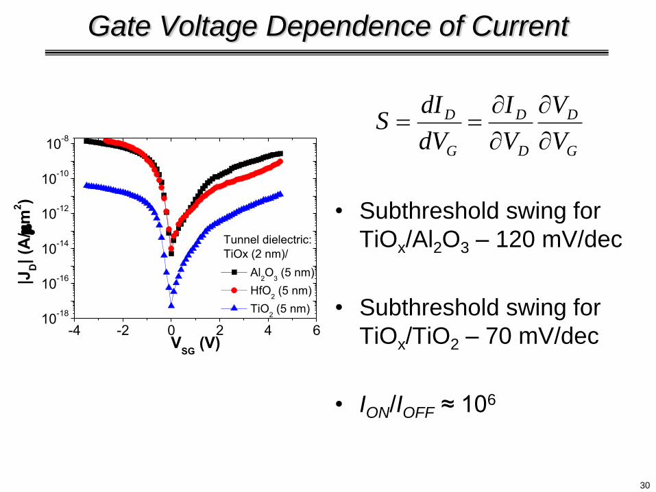
Gate Voltage Dependence of Current
• Subthreshold swing for
TiOx/Al2O3 – 120 mV/dec
• Subthreshold swing for
TiOx/TiO2 – 70 mV/dec
• ION/IOFF ≈ 106
G
D
D
D
G
D
V
V
V
I
dV
dIS
-4 -2 0 2 4 610
-18
10-16
10-14
10-12
10-10
10-8
Tunnel dielectric:
TiOx (2 nm)/
|JD|
(A/
m2)
VSG
(V)
Al2O
3 (5 nm)
HfO2 (5 nm)
TiO2 (5 nm)

31
Drain Voltage Dependence of Current
• Upon decoupling gate oxide
capacitance
– “subthreshold swing”
(∂ID/∂VD)-1 ≈ 27 mV/dec for
TiOx (2 nm)/TiO2 (5 nm)
– 10 mV/dec for TiOx (1
nm)/Al2O3 (1 nm)/TiO2 (1 nm)
G
D
D
D
G
D
V
V
V
I
dV
dIS
• Symmetric current for symmetric barrier
• Drive current extremely low
-4
-3
-2
-1
Gra
ph
en
e
Al2O
3
TiO
x
En
erg
y (
eV
)
TiO
x
Al2O
3
Gra
ph
en
e
Gra
ph
en
e
Gra
ph
en
e
Energy band diagram
VD > 0 V VD < 0 V
-1.0 -0.5 0.0 0.5 1.010
-17
10-15
10-13
10-11
10-9
10-7
JD (
A/
m2)
Vtox
(V)
TiOx/Al
2O
3
(2 nm/ 5 nm)
TiOx/TiO
2
(2 nm/ 5 nm)
TiOx/ HfO
2
(2 nm/ 5 nm)
TiOx/Al
2O
3/TiO
2
(1 nm/ 1 nm/ 1 nm)
h-BN (~ 5-7 layers),
VG = -5 V
[1]
h-BN (~ 5-7 layers)
VG = +5 V
[1]

32
• Motivation
• A Simple “Universal” Model for Transport in Single Layer Graphene
• Effect of Device Dimensions on Mobility
• Effect of Contacts
• CVD Graphene Vertical Tunnel Transistors
• Conclusions
Outline 5

33
Conclusions
• A simple model for the total device resistance indicates that the
maximum graphene resistance is approximately independent of mobility
and that the minimum resistance is limited by the contact resistance.
• Mobility depends on both the device length and width. Large device
dimensions should be used when extracting mobility.
•Current saturation at large fields is due to the contact resistance.
• The width dependence of contact resistance suggests preferential
injection at the edges of graphene.
• A transfer process for CVD graphene has been developed which
achieves mobility consistent with exfoliated graphene.
• Vertical tunnel FETs have been fabricated using bilayers of CVD
graphene.