Issue Date:Mar 23, 2015 ML22Q321/321 · Issue Date:Mar 23, 2015 ML22Q321/321 ADPCM Speech Synthesis...
35
FEDL22321-01 Issue Date:Mar 23, 2015 ML22Q321/321 ADPCM Speech Synthesis LSI 1/35 GENERAL DESCRIPTION The ML22321/ML22Q321, which include mask ROM and Flash memory for storing speech data, respectively, are speech synthesis LSIs which can control speech playback utilizing a serial interface. It includes speaker amplifier and 16bit DA Converter, so it is possible to have high quality sound and solution for playback with 1chip. • Playback Time Maximum Playback time(s) (Fsam=8.0kHz) Product Name Capasitance of ROM(bit) HQ-ADPCM 4bitADPCM2 16bitPCM ML22Q321/321 920K 36.8 29.4 7.3 • Speech sysnthesis system: 4-bit ADPCM2 8-bit/16-bit straight PCM system 8-bit nonlinear PCM system HQ-ADPCM(*1) (can be specified for each phrase) • Speech ROM capacity ML22321: 920-Kbit Mask ROM ML22Q321: 920-Kbit Flash • Sampling frequency: 8.0/16.0 /32.0kHz, 6.4/12.8/25.6 kHz/, 10.7/21.3 kHz (fsam can be specified in units of phrase) • Volume control function: 32 steps by an analog value input and ADC (OFF is included) • Analog output: Built-in 16-bit DA converter • Interface: Synchronous serial interface MSB first, LSB first, or default level of synchronous clock is selectable based on ROM data • Maximum event count: 62 events • Source oscillation frequency: 4.096 MHz (Typ.) • Power supply voltage: 2.3V to 5.5V • Flash memory rewrite cycles 80 times (ML22Q321) • Operating temperature range: −40°C to +85°C • Package: 30-pin plastic SSOP (SSOP30-56-0.65-Z6K9-MC) • Product name: ML22321-xxxMB (xxx: ROM code number) ML22Q321-NNNMB/ML22Q321-xxxMB(xxx: ROM code number) HQ-ADPCM is audio compression technology featuring high-quality sound. It was developed by “Ky’s”. “Ky’s” is a registered trademark of Kyushu Institute of Technology, one of the national universities in Japan. (*1)
Transcript of Issue Date:Mar 23, 2015 ML22Q321/321 · Issue Date:Mar 23, 2015 ML22Q321/321 ADPCM Speech Synthesis...

FEDL22321-01Issue Date:Mar 23, 2015
ML22Q321/321 ADPCM Speech Synthesis LSI
1/35
GENERAL DESCRIPTION The ML22321/ML22Q321, which include mask ROM and Flash memory for storing speech data, respectively, are speech synthesis LSIs which can control speech playback utilizing a serial interface. It includes speaker amplifier and 16bit DA Converter, so it is possible to have high quality sound and solution for playback with 1chip. • Playback Time
Maximum Playback time(s) (Fsam=8.0kHz) Product Name Capasitance of ROM(bit) HQ-ADPCM 4bitADPCM2 16bitPCM
ML22Q321/321 920K 36.8 29.4 7.3 • Speech sysnthesis system: 4-bit ADPCM2
8-bit/16-bit straight PCM system 8-bit nonlinear PCM system HQ-ADPCM(*1) (can be specified for each phrase)
• Speech ROM capacity ML22321: 920-Kbit Mask ROM ML22Q321: 920-Kbit Flash
• Sampling frequency: 8.0/16.0 /32.0kHz, 6.4/12.8/25.6 kHz/, 10.7/21.3 kHz (fsam can be specified in units of phrase)
• Volume control function: 32 steps by an analog value input and ADC (OFF is included) • Analog output: Built-in 16-bit DA converter • Interface: Synchronous serial interface MSB first, LSB first, or default level of synchronous clock is selectable based on ROM data • Maximum event count: 62 events • Source oscillation frequency: 4.096 MHz (Typ.) • Power supply voltage: 2.3V to 5.5V • Flash memory rewrite cycles 80 times (ML22Q321) • Operating temperature range: −40°C to +85°C • Package: 30-pin plastic SSOP (SSOP30-56-0.65-Z6K9-MC) • Product name: ML22321-xxxMB (xxx: ROM code number)
ML22Q321-NNNMB/ML22Q321-xxxMB(xxx: ROM code number)
HQ-ADPCM is audio compression technology featuring high-quality sound. It was developed by “Ky’s”.“Ky’s” is a registered trademark of Kyushu Institute of Technology, one of the national universities in Japan.
(*1)

FEDL22321-01
ML22Q321/321
2/35
BLOCK DIAGRAM ML22Q321-NNN/ML22Q321-xxx
Timing Controller
SPI
Interface
Phrase Address Latch
Address
Controller
16bit Address Counter
LPF
16bit DAC
AOUT
CSBSCKSIN
TESTTESTI0TESTI1
BUSYBSCKEN
ERRTESTO
VDD
GND
OSC0
OSC
RESET_N
I/O
Interface
16bit Multiplexer
ADPCM/PCM Synthesizer
920Kbit Flash
Regulator
VDDL
VPP
OSC1
SP
AMP SPVDD
SPGND
SPM
SPP
SG SPOFF
VREF

FEDL22321-01
ML22Q321/321
3/35
ML22321-xxx
Timing Controller
SPI
Interface
Phrase Address Latch
Address
Controller
16bit Address Counter
LPF
16bit DAC
AOUT
CSBSCKSIN
TESTTESTI0TESTI1
BUSYBSCKEN
ERRTESTO
VDD
GND
OSC0
OSC
RESET_N
I/O
Interface
16bit Multiplexer
ADPCM/PCM Synthesizer
920Kbit ROM
Regulator
VDDL
OSC1
SP
AMP SPVDD
SPGND
SPM
SPP
SG SPOFF
VREF

FEDL22321-01
ML22Q321/321
4/35
PIN CONFIGURATION (TOP VIEW) ML22Q321-NNNMB/ML22Q321-xxxMB
30-pin Plastic SSOP ML22321-xxxMB
30-pin Plastic SSOP
VDD
OSC0OSC1
VDDL
VPP
ERRTESTO
SCKSIN
GNDRESET_N
TESTSPOFFTESTI1TESTI0
1 2 3 4 5 6 7 8 9 10 11 12 13 14 15
SPP SPM (NC) SPGND SPVDD
SPIN AOUT SG GND
SCKEN BUSYB CSB VDD GND VREF
302928272625242322212019181716
NC:unused pin
VDD
OSC0OSC1
VDDL
(NC)ERR
TESTOSCKSIN
GNDRESET_N
TESTSPOFFTESTI1TESTI0
1 2 3 4 5 6 7 8 9 10 11 12 13 14 15
SPP SPM (NC) SPGND SPVDD
SPIN AOUT SG GND
SCKEN BUSYB CSB VDD GND VREF
302928272625242322212019181716
NC:unused pin

FEDL22321-01
ML22Q321/321
5/35
PIN DESCRIPTIONS
Pin No. symbol I/O Description
11 RESET_N I Place this pin at a “L” level when powered on. After the supply voltage is settled, place this pin at a “H” level.
19 CSB I Chip select pin. At the “L” level, SCK0 pin and SIN0 pin are available.
8 SCK I Synchronous clock input pin for serial interface. 9 SIN I Input pin of synchronous serial data.
13 SPOFF I Control pin of internal speaker amplifier. In “H” level input, internal speaker amplifier is turned off.
16 VREF I Volume control pin. Input the voltage of the range from VDD to GND. Volume is the maximum when input voltage is VDD.
12 TEST I Input pin for testing. Fix this pin at a “L” level (GND level). 15 TESTI0 I Input pin for testing. Fix this pin at a “L” level (GND level). 14 TESTI1 I Input pin for testing. Fix this pin at a “L” level (GND level).
2 OSC0 I Pin for connecting a crystal or a ceramic vibrator. A feed back resistor (about 1 MΩ) is included between OSC0 and OSC1 pins. When a vibrator is used, place it as close to the LSI as possible.
3 OSC1 O Pin for connecting a crystal or a ceramic vibrator. When a vibrator is used, place it as close to the LSI as possible.
20 BUSYB O
Playback status signal output pin. "L" is outputted when an event is fixed. After playback is completed, “H” is outputted after WS3. Then, when the POP noise measure is completed, it turns standby state.
21 SCKEN O Output pin showing the permission state of SCK input of a serial interface The input of SCK and SIN is permitted during H" level output, and it is disregarded during H" level output
6 ERR O
Error output pin for thermal detection and disconnection detection. If disconnection detection or a higher temperature than the judgment temperature is detected, this pin output “H”. Setting event 1 , operate the disconnection detection. And the 100ms “H” pulse is output right after the event start.
24 AOUT O Playback signal output pin. When you use built-in speaker amplifier, connect with the SPIN pin.
7 TESTO O Output pin for test.
5 VPP *Note 1 — Power supply pin for rewriting Flash memory.
Fix this pin to GND except when rewriting Flash memory.
1,18 VDD — Digital power supply pin. Connect a capacitor of 0.1 µF or more between this pin and GND.
4 VDDL — Output pin of the regulator for the internal logic power supply. Connect a electrolytic capacitor of 10 uF or more and a ceramic capacitor of 0.1 µF or more between the VDDL and GND pins.
10,17,22 GND — Digital ground pin. 27 SPGND — Speaker amplifier ground pin. 26 SPVDD — Speaker amplifier power supply pin. 25 SPIN I Analog input pin of internal speaker amplifier.
23 SG O Built-in speaker amplifier’s reference voltage output pin. Connect a capacitor of 0.1 µF or more between this pin and GND.
30 SPP O Positive output pin of the built-in speaker amplifier. 29 SPM O Negative output pin of the built-in speaker amplifier.
Notes: 1. Applies to ML22Q321-NNN
FEDL22321-01
ML22Q321/321
6/35
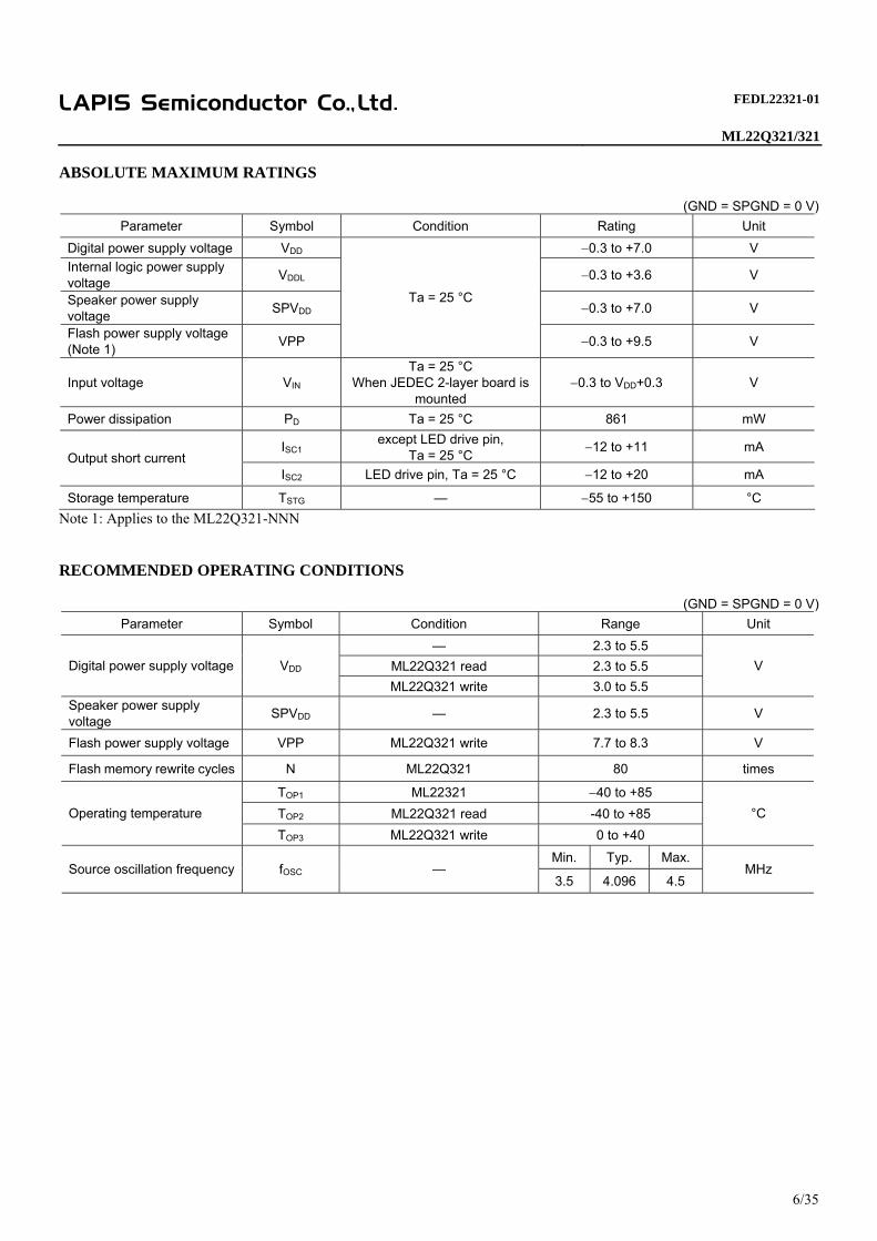
ABSOLUTE MAXIMUM RATINGS
(GND = SPGND = 0 V) Parameter Symbol Condition Rating Unit
Digital power supply voltage VDD −0.3 to +7.0 V Internal logic power supply voltage VDDL −0.3 to +3.6 V
Speaker power supply voltage SPVDD −0.3 to +7.0 V
Flash power supply voltage (Note 1) VPP
Ta = 25 °C
−0.3 to +9.5 V
Input voltage VIN Ta = 25 °C
When JEDEC 2-layer board is mounted
−0.3 to VDD+0.3 V
Power dissipation PD Ta = 25 °C 861 mW
ISC1 except LED drive pin,
Ta = 25 °C −12 to +11 mA Output short current
ISC2 LED drive pin, Ta = 25 °C −12 to +20 mA
Storage temperature TSTG — −55 to +150 °C Note 1: Applies to the ML22Q321-NNN RECOMMENDED OPERATING CONDITIONS
(GND = SPGND = 0 V) Parameter Symbol Condition Range Unit
— 2.3 to 5.5 ML22Q321 read 2.3 to 5.5 Digital power supply voltage VDD ML22Q321 write 3.0 to 5.5
V
Speaker power supply voltage SPVDD — 2.3 to 5.5 V
Flash power supply voltage VPP ML22Q321 write 7.7 to 8.3 V
Flash memory rewrite cycles N ML22Q321 80 times
TOP1 ML22321 −40 to +85 TOP2 ML22Q321 read -40 to +85 Operating temperature TOP3 ML22Q321 write 0 to +40
°C
Min. Typ. Max. Source oscillation frequency fOSC —
3.5 4.096 4.5 MHz

FEDL22321-01
ML22Q321/321
7/35
ELECTRICAL CHARACTERISTICS DC Characteristics
VDD = SPVDD = 2.3 to 5.5 V, GND = SPGND = 0 V, Ta = −40 to +85°C Parameter Symbol Condition Min. Typ. Max. Unit
“H” input voltage VIH — 0.7×VDD — VDD V “L” voltage VIL — 0 — 0.3×VDD V “H” output voltage 1 VOH1 IOH = −0.5 mA VDD−0.5 — — V
“H” output voltage 2 VOH2 IOH = 100µA OSC1 pin VDD−0.5 — — V
“L” output voltage 1 VOL1 IOL = 0.5 mA — — 0.5 V
“L” output voltage 2 VOL2 IOL = 100µA OSC1 pin — — 0.5 V
“H” input current 1 IIH1 VIH = VDD — — 1 µA
“H” input current 2 IIH2 VIH = VDD
TEST, TESTI0, TESTI1 pin 0.02 0.3 1.5 mA
“L” input current 1 IIL1 VIL = GND −1 — — µA
“L” input current 2 IIL2 VIL = GND
RESET_N pin −1.5 −0.3 −0.02 mA
IDD1 Non-loaded output
VDD = SPVDD = 3.0V — 2.5 12 Supply current during
operate IDD2 Non-loaded output
VDD = SPVDD = 5.0V — 8 12 mA
IDDS1 Ta ≦40°C — 0.5 2.0 Supply current during power down IDDS2 Ta ≦ 85°C — 0.5 8.0
µA
Analog Characteristics
VDD = SPVDD = 2.3 to 5.5 V, GND = SPGND = 0 V, Ta = −40 to +85°C Parameter Symbol Condition Min. Typ. Max. Unit
AOUT output load resistance RLA During 1/2 VDD output 10 — — kΩ
AOUT output voltage range VAO No output load 1/6×VDD — 5/6×VDD V SG output voltage VSG ⎯ 0.95xVDD/2 VDD/2 1.05xVDD/2 V SG output resistance RSG ⎯ 57 96 135 kΩ SPM, SPP output load resistance RLSP ⎯ 8 ⎯ ⎯ Ω
Speaker amplifier output power PSPO SPVDD=5.0V,f=1kHz , RSPO=8Ω,THD≧10%
⎯ 1 ⎯ W
Output offset voltage between SPMand SPP with no signal present VOF
SPIN-SPM gain=0dB 8Ω load
-50 ⎯ 50 mV
FEDL22321-01
ML22Q321/321
8/35
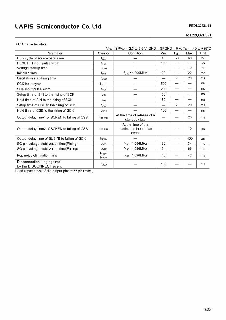
AC Characteristics VDD = SPVDD = 2.3 to 5.5 V, GND = SPGND = 0 V, Ta = −40 to +85°C
Parameter Symbol Condition Min. Typ. Max. Unit Duty cycle of source oscillation fduty — 40 50 60 % RESET_N input pulse width tRST — 100 — — µs Voltage startup time tPWR — — — 10 ms Initialize time tINIT fOSC=4.096MHz 20 — 22 ms Oscillation stabilizing time tOSC — — 2 20 ms SCK input cycle tSCYC — 500 — — ns
SCK input pulse width tSW — 200 — — ns
Setup time of SIN to the rising of SCK tSS — 50 — — ns
Hold time of SIN to the rising of SCK tSH — 50 — — ns Setup time of CSB to the rising of SCK tCSS — — 2 20 ms Hold time of CSB to the rising of SCK tCSH — 100 — — ns
Output delay time1 of SCKEN to falling of CSB tDSEN1 At the time of release of a
standby state — — 20 ms
Output delay time2 of SCKEN to falling of CSB tDSEN2 At the time of the
continuous input of an event
— — 10 µs
Output delay time of BUSYB to falling of SCK tDBSY — — — 400 µs SG pin voltage stabilization time(Rising) tSGR fOSC=4.096MHz 32 — 34 ms SG pin voltage stabilization time(Falling) tSGF fOSC=4.096MHz 64 — 66 ms
Pop noise elimination time tPOPR
tPOPF fOSC=4.096MHz 40 — 42 ms
Disconnection judging time by the DISCONNECT event tDCD — 100 — — ms
Load capacitance of the output pins = 55 pF (max.)
FEDL22321-01
ML22Q321/321
9/35
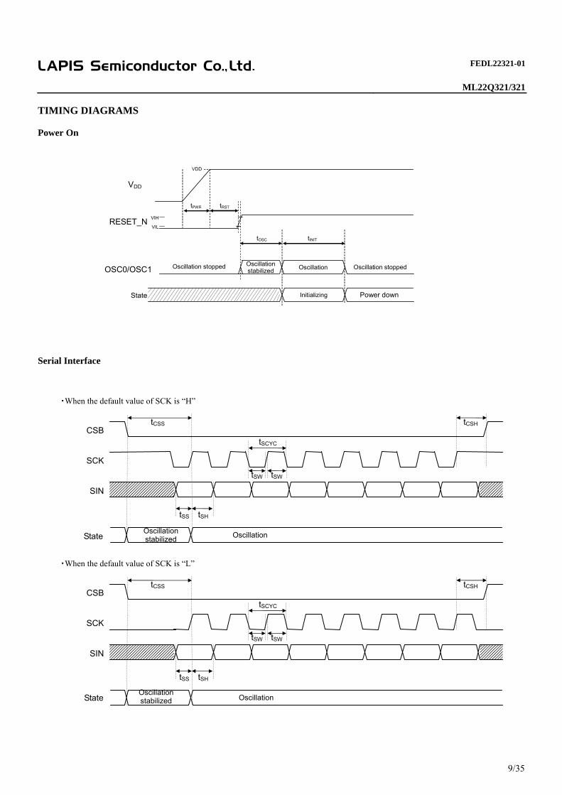
TIMING DIAGRAMS Power On Serial Interface
CSB
・When the default value of SCK is “H”
SCK
SIN
tCSS
tSS tSH
tSW
tSCYC
tSW
tCSH
CSB
・When the default value of SCK is “L”
SCK
SIN
tCSS
tSS tSH
tSW
tSCYC
tSW
tCSH
StateOscillation stabilized Oscillation
State OscillationOscillation stabilized
VDD
VIH
VIL
tRST
VDD
RESET_N
State
OSC0/OSC1
tINITtOSC
tPWR
Oscillation stabilized
Oscillation stopped Oscillation Oscillation stopped
Initializing Power down

FEDL22321-01
ML22Q321/321
10/35
Event Control example 1 (Only one playback in Play once mode)
Oscillation stopped
tOSC
State
Oscillation stabilized
Power down
Power down
AOUT GND
Wait time after fixing event
WS1
Executing event n (Play once mode)
Oscillation stopped
OSC0OSC1 Oscillation
Eliminating pop noise
Eliminating pop noise
WS2
Wait time before play
Wait time after play
WS3
Wait time before power down
WS4tSGR tPOPR tSGFtPOPF
Eliminating noise
Event n
SIN
CSB
Event state
invalid commandEvent activation
Event m
Stop playSCK
SCKEN
BUSYB
tDSEN2tDSEN1
tDBSY

FEDL22321-01
ML22Q321/321
11/35
Event Control example 2 (Only one playback in Scheduled play mode)
Oscillation stopped
tOSC
State
Oscillation stabilized
Power down
Power down
AOUT GND
Wait time after fixing event
WS1
Executing event n (Scheduled play mode)
Oscillation stopped
OSC0OSC1 Oscillation
Eliminating pop noise
Eliminating pop noise
WS2
Wait time before play
Wait time after play
WS3
Wait time before power down
WS4tSGR tPOPR tSGFtPOPF
Eliminating noise
Event n
SIN
CSB
Event state
Fixed event “00”Event activation
”00” Stop play
SCK
SCKEN
BUSYB
tDSEN2tDSEN1
tDBSY

FEDL22321-01
ML22Q321/321
12/35
Event Control example 3 (Repetitive playback in Scheduled play mode)
Oscillation stopped
tOSC
State
Oscillation stabilized
Power down
Power down
AOUT GND
Wait time after fixing event
WS1
Executing event n (Scheduled play mode)
Oscillation stopped
OSC0OSC1 Oscillation
ポップノイズ対策中
Eliminating pop noise
WS2
Wait time before play
Wait time after play
WS3
Wait time before power down
WS4 tSGR tPOPR tSGFtPOPF
Inputting event
Event n
SIN
CSB
Event state
Fixed event “00”
”00” Stop play
SCK
SCKEN
Event activation
Play event n continuously BUSYB
tDSEN2tDSEN1
tDBSY

FEDL22321-01
ML22Q321/321
13/35
Event Control example 4 (Change in playback phrase in Scheduled play mode)
Oscillation stopped
tOSC
State
Oscillation stabilized
Power down
Power down
AOUT GND
Wait time after fixing event
WS1
Executing event n (Scheduled play mode)
Oscillation stopped
OSC0OSC1 Oscillation
Eliminating pop noise
Eliminating pop noise
WS2
Wait time before play
Wait time after play
WS3
Wait time before power down
WS4 tSGR tPOPR tSGFtPOPF
Inputting event
SIN
CSB
Event state
Fixed event “00”Event activation
”00”
Stop play
SCK
SCKEN
Play event n continuously
Event n
Fixed event m
Event m
Executing event m (Scheduled play mode)
Play event m BUSYB
tDSEN2 tDSEN2tDSEN1
tDBSY

FEDL22321-01
ML22Q321/321
14/35
Event Control example 5 (Repetitive playback in Change immediately mode)
Oscillation stopped
tOSC
State
Oscillation stabilized
Power down
Power down
AOUT GND
Wait time after fixing event
WS1
Executing event n (Change immediately mode)
Oscillation stopped OSC0OSC1 Oscillation
Eliminating pop noise
Eliminating pop noise
WS2
Wait time before play
Wait time after play
WS3
Wait time before power down
WS4tSGR tPOPR tSGFtPOPF
Eliminating noise
Event n
SIN
CSB
Event state
Stop event n immediately
Event activation
”00”
SCK
SCKEN
Play event n continuously BUSYB
tDSEN2tDSEN1
tDBSY

FEDL22321-01
ML22Q321/321
15/35
Event Control example 6 (Different consecutive event execution timing diagram in Change immediately mode)
Oscillation stopped
tOSC
State
Oscillation stabilized
Power down
Power down
AOUT GND
Wait time after fixing event
WS1
Executing event n (Change immediately mode)
Oscillation stopped
OSC0OSC1 Oscillation
Eliminating pop noise
Eliminating pop noise
WS2
Wait time before play
Wait time after play
WS3
Wait time before power down
WS4tSGR tPOPR tSGFtPOPF
Eliminating noise
SIN
CSB
Event state
Stop event m immediately
Event activation
”00”
SCK
SCKEN
Play event n continuously
Event n
Change event n immediately
Event m
Executing event m (Scheduled play mode)
Event m PlayBUSYB
tDSEN2tDSEN2tDSEN1
tDBSY

FEDL22321-01
ML22Q321/321
16/35
FUNCTIONAL DESCRIPTION The "Speech LSI Utility” is used for the setting of an each function and the creating of ROM data. The Speech LSI Utility is dedicated software. Serial interface input flow chart The timing to which the input of serial interface is permitted can be judged by monitoring the output of SCKEN. The flow chart is shown below.
Event fix (8bit input)
Event input(SCK,SIN input)
End
SCKEN ”H”
Y
N
N
Start
CSB ”L”input
Y
CSB ”H”input
FEDL22321-01
ML22Q321/321
17/35
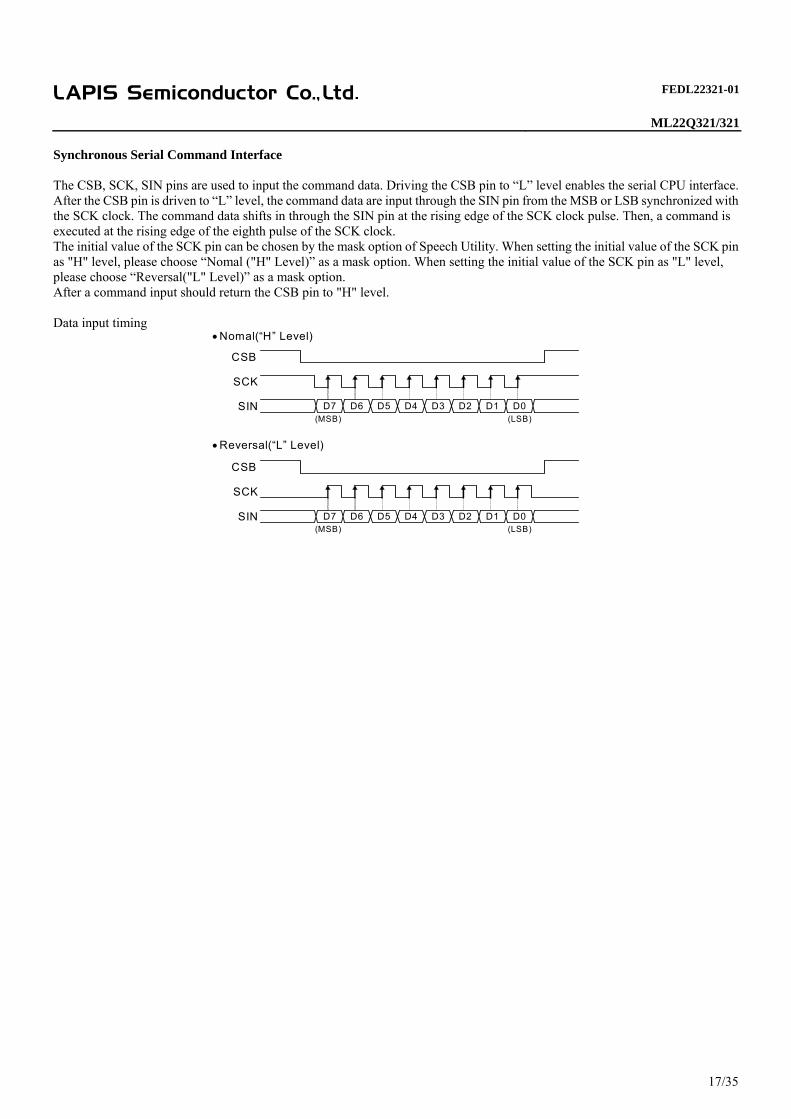
Synchronous Serial Command Interface The CSB, SCK, SIN pins are used to input the command data. Driving the CSB pin to “L” level enables the serial CPU interface. After the CSB pin is driven to “L” level, the command data are input through the SIN pin from the MSB or LSB synchronized with the SCK clock. The command data shifts in through the SIN pin at the rising edge of the SCK clock pulse. Then, a command is executed at the rising edge of the eighth pulse of the SCK clock. The initial value of the SCK pin can be chosen by the mask option of Speech Utility. When setting the initial value of the SCK pin as "H" level, please choose “Nomal ("H" Level)” as a mask option. When setting the initial value of the SCK pin as "L" level, please choose “Reversal("L" Level)” as a mask option. After a command input should return the CSB pin to "H" level. Data input timing
• Nomal(“H” Level)
• Reversal(“L” Level)
CSB
SCK
SIN D7 D6 D5 D4 D3 D2 D1 D0(MSB) (LSB)
CSB
SCK
SIN D7 D6 D5 D4 D3 D2 D1 D0(MSB) (LSB)

FEDL22321-01
ML22Q321/321
18/35
Playback mode setup Playback mode can be set up for every phrase. Playback mode is set into the ROM data. The ROM data is created using a Speech LSI Utility. The Speech LSI Utility is dedicated software.
Playback mode Operation
Play Once This mode is playback once. All the commands become invalid during playback.
Scheduled Play The playback continues until the following command will be inputted, if playback starts. When the following command is inputted into playback, after playback of the present phrase is completed, the following command is executed.
Change Immediately The playback continues until the following command will be inputted, if playback starts. When the following phrase is inputted into playback, playback of the present phrase is ended on the way, and playback of the following phrase starts.
Event List Each event is configured by the unit of byte (8-bit).
Event D7 D6 D5 D4 D3 D2 D1 D0 Description
Stop 0 0 0 0 0 0 0 0
Stop event. The Stop event becomes effective except the phrase in Play Once mode.
Disconnection Detection 0 0 0 0 0 0 0 1
Disconnection Detection event. Please input the Stop event, after you use the Disconnection Detection event.
0 0 0 0 0 0 1 0 PHRASE02 0 0 0 0 0 0 1 1 PHRASE03
: : 0 0 0 0 1 0 0 1 PHRASE09 0 0 0 0 1 0 1 0 PHRASE0A
: :
Play
0 0 1 1 1 1 1 1 PHRASE3F

FEDL22321-01
ML22Q321/321
19/35
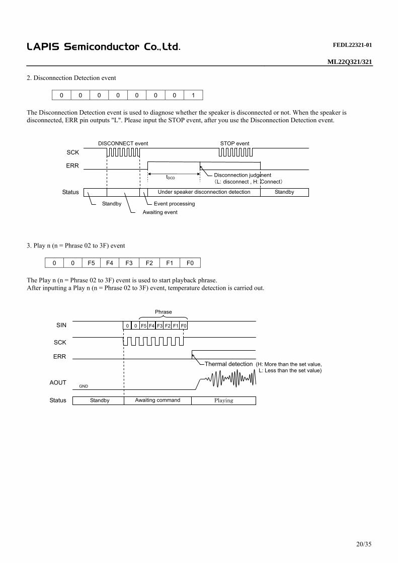
Description of Command Functions 1. Stop event
0 0 0 0 0 0 0 0 The Stop event is used to stop the repetitive playback. The Stop event becomes effective except the phrase in Play Once mode. When you use Play Once mode, the Stop event is ignored. When you use Scheduled Play mode, a phrase is played back to the last and the playback is stopped, after the Stop event is inputted.
Furthermore, when you use Change Immediately mode, a phrase is not played back to the last and the playback is stopped forcibly, after the Stop event is inputted.
Stop event operation in the case of Scheduled Play mode
Stop event operation in the case of Change Immediately mode
SCK
AOUT
Status
Phrase
GND
STOP event
Standby
Playing Event processing
Standby
Awaiting event
SCK
AOUT
Status
Phrase
GND
STOP event
Standby
Playing (playback to the last)
Event processing Standby Awaiting event
FEDL22321-01
ML22Q321/321
20/35
2. Disconnection Detection event
0 0 0 0 0 0 0 1 The Disconnection Detection event is used to diagnose whether the speaker is disconnected or not. When the speaker is disconnected, ERR pin outputs "L". Please input the STOP event, after you use the Disconnection Detection event.
3. Play n (n = Phrase 02 to 3F) event
0 0 F5 F4 F3 F2 F1 F0 The Play n (n = Phrase 02 to 3F) event is used to start playback phrase. After inputting a Play n (n = Phrase 02 to 3F) event, temperature detection is carried out.
SIN
AOUT
Status
Phrase
GND
Awaiting command Standby Playing
0 F5 F4 F3 F2 F1 F00
SCK
ERR Thermal detection (H: More than the set value,
L: Less than the set value)
SCK
ERR
Status
DISCONNECT event STOP event
Standby
Under speaker disconnection detection Event processing
Standby
tDCDDisconnection judgment (L: disconnect , H: Connect)
Awaiting event

FEDL22321-01
ML22Q321/321
21/35
Event Control example 1 (Only one playback in Play once mode) Operation: The specified event is performed once after event starting. Other event inputs are disregarded during event
execution. Control method: Input the event number to be executed to the serial interface pins.
Event Control example 2 (Only one playback in Scheduled play mode) Operation: The specified event is performed once. Control method: Input the event number to be executed to the serial interface pins. In this mode, the event fixed at the time of
the end of phrase playback is performed repeatedly. Therefore, after event activation, input stop event"00" into the serial interface pins before the event is completed.
Event Control example 3 (Repetitive playback in Scheduled play mode) Operation: After an event starts, unless a stop command is inputted, the event is performed repetitively.
When a stop event is inputted, the event under execution is performed to the last and stops. Control method: Input the event number to be executed to the serial interface pins. In this mode, the event fixed at the time of
the end of phrase playback is performed repeatedly. After an event starts, unless a stop command is inputted, the event is performed repetitively. When desired to stop event execution, input stop command to the serial interface pins.
“Good morning”
CSB
SCK
SIN
Event n
“Good morning”
CSB
SCK
SIN
Event n 00h
“Good morning”
CSB
SCK
SIN
Event n 00h
“Good morning”

FEDL22321-01
ML22Q321/321
Event Control example 4 (Change in playback phrase in Scheduled play mode) Operation: The event execution specified first is ended and newly specified event execution is started. Control method: Input the event number to be executed to the serial interface pins. In this mode, the event fixd at the time of
the end of phrase playback is performed repeatedly. Therefore, after event activation, input a new event into the serial interface pins before the event is completed.
Event Control example 5 (Repetitive playback in Change immediately mode) Operation: After an event starts, unless a stop command is inputted, the event is performed repetitively.
When a stop event is inputted, the event stops immediately. Control method: Input the event number to be executed to the serial interface pins. When desired to stop event execution,
input stop command to the serial interface pins. the event stops immediately.
Event Control example 6 (Change in playback phrase in Change immediately mode) Operation: The event under execution is immediately changed into a new event. Control method: Input the event number to be executed to the serial interface pins. After an event starts, input the next event
number to the serial interface pins. The event under execution is immediately changed into a new event.
“Good morning”
CSB
SCK
SIN
Event n 00h
“Good afternoon”
Event m
“Good morning”
CSB
SCK
SIN
Event n 00h
“Good mor
CSB
SCK
SIN
Event n 00h Event m
“Good mor
“Good morning” “Good after22/35

FEDL22321-01
ML22Q321/321
23/35
Wait time setting before and after playback (WS1, WS2, WS3, WS4) Each phrase can set up the wait time before and after playback. It is set into the ROM. The ROM data is created using a Speech LSI Utility. The Speech LSI Utility is dedicated software.
WS1: Time after inputting a phrase address, until SPP/SPM pins are enabled. WS2: Time after SPP/SPM pins are enabled, until playback is started. WS3: Time after playback is completed, until SPP/SPM pins are disabled. WS4: Time after SPP/SPM pins are disabled, until it will be in a standby state.
WS1-WS4 can be arbitrarily set up between 0 to1020ms (4ms unit).
SCK
AOUT
Status
Phrase
GND
Standby
Playing Event processing
Standby
WS1 WS2 WS3 WS4
Awaiting event

FEDL22321-01
ML22Q321/321
24/35
Wait time setting before and after playback (WS1, WS2, WS3, WS4) Setting value
wait time [ms]
Setting value
wait time [ms]
Settingvalue
wait time[ms]
Settingvalue
wait time[ms]
Setting value
wait time[ms]
00h 0 34h 208 67h 412 9Ah 616 CDh 820 01h 4 35h 212 68h 416 9Bh 620 CEh 824 02h 8 36h 216 69h 420 9Ch 624 CFh 828 03h 12 37h 220 6Ah 424 9Dh 628 D0h 832 04h 16 38h 224 6Bh 428 9Eh 632 D1h 836 05h 20 39h 228 6Ch 432 9Fh 636 D2h 840 06h 24 3Ah 232 6Dh 436 A0h 640 D3h 844 07h 28 3Bh 236 6Eh 440 A1h 644 D4h 848 08h 32 3Ch 240 6Fh 444 A2h 648 D5h 852 09h 36 3Dh 244 70h 448 A3h 652 D6h 856 0Ah 40 3Eh 248 71h 452 A4h 656 D7h 860 0Bh 44 3Fh 252 72h 456 A5h 660 D8h 864 0Ch 48 40h 256 73h 460 A6h 664 D9h 868 0Dh 52 41h 260 74h 464 A7h 668 DAh 872 0Eh 56 42h 264 75h 468 A8h 672 DBh 876 0Fh 60 43h 268 76h 472 A9h 676 DCh 880 10h 64 44h 272 77h 476 AAh 680 DDh 884 11h 68 45h 276 78h 480 ABh 684 DEh 888 12h 72 46h 280 79h 484 ACh 688 DFh 892 13h 76 47h 284 7Ah 488 ADh 692 E0h 896 14h 80 48h 288 7Bh 492 AEh 696 E1h 900 15h 84 49h 292 7Ch 496 AFh 700 E2h 904 16h 88 4Ah 296 7Dh 500 B0h 704 E3h 908 17h 92 4Bh 300 7Eh 504 B1h 708 E4h 912 18h 96 4Ch 304 7Fh 508 B2h 712 E5h 916 19h 100 4Dh 308 80h 512 B3h 716 E6h 920 1Ah 104 4Eh 312 81h 516 B4h 720 E7h 924 1Bh 108 4Fh 316 82h 520 B5h 724 E8h 928 1Ch 112 50h 320 83h 524 B6h 728 E9h 932 1Dh 116 51h 324 84h 528 B7h 732 EAh 936 1Eh 120 52h 328 85h 532 B8h 736 EBh 940 1Fh 124 53h 332 86h 536 B9h 740 ECh 944 20h 128 54h 336 87h 540 BAh 744 EDh 948 21h 132 55h 340 88h 544 BBh 748 EEh 952 22h 136 56h 344 89h 548 BCh 752 EFh 956 23h 140 57h 348 8Ah 552 BDh 756 F0h 960 24h 144 58h 352 8Bh 556 BEh 760 F1h 964 25h 148 59h 356 8Ch 560 BFh 764 F2h 968 26h 152 5Ah 360 8Dh 564 C0h 768 F3h 972 27h 156 5Bh 364 8Eh 568 C1h 772 F4h 976 28h 160 5Ch 368 8Fh 572 C2h 776 F5h 980 29h 164 5Dh 372 90h 576 C3h 780 F6h 984 2Ah 168 5Eh 376 91h 580 C4h 784 F7h 988 2Bh 172 5Fh 380 92h 584 C5h 788 F8h 992 2Ch 176 60h 384 93h 588 C6h 792 F9h 996 2Dh 180 61h 388 94h 592 C7h 796 FAh 1000 2Eh 184 62h 392 95h 596 C8h 800 FBh 1004 2Fh 188 63h 396 96h 600 C9h 804 FCh 1008 30h 192 64h 400 97h 604 CAh 808 FDh 1012 31h 196 65h 404 98h 608 CBh 812 FEh 1016 32h 200 66h 408 99h 612 CCh 816 FFh 1020 33h 204

FEDL22321-01
ML22Q321/321
25/35
Volume control (Volume) Use or unuse of volume control setting by the external VREF input is selectable. When not using the external VREF input function, the VREF input value becomes null, and it comes to be able to setup volume by ROM data in each phrase. When using an external VREF input function, the analog value inputted from VREF is changed into 32 steps of volume preset values by ADC. Taking in of a VREF value is carried out every about 10ms. In this case, the volume setup by ROM data becomes null. And volume setting is as follows.
Setting value Volume [dB] Setting value Volume [dB] Setting value Volume [dB] 00h +2.98 0Ah -0.41 15h -6.87 01h +2.70 0Bh -0.83 16h -7.79 02h +2.40 0Ch -1.28 17h -8.82 03h +2.10 0Dh -1.75 18h -9.99 04h +1.78 0Eh -2.25 19h -11.34 05h +1.45 0Fh -2.77 1Ah -12.94 06h +1.11 10h -3.34 1Bh -14.90 07h +0.76 11h -3.94 1Ch -17.44 08h +0.39 12h -4.58 1Dh -21.04 09h +0.00 13h -5.28 1Eh -27.31
14h -6.04 1Fh OFF

FEDL22321-01
ML22Q321/321
26/35
Mask Option Setting The following table shows the items which can be set by using the Mask option (ROM data): During initialization processing after power on, mask option data are transferd automatically to each setting. The ROM data is created using a Speech LSI Utility. The Speech LSI Utility is dedicated software.
Function Description Parameter Speaker Amp control Setting of the internal
speaker amplifier Use or unuse of the internal speaker amplifier selectable
Use of Speaker Amp Speaker Amp control
Gain +6dB
Setting of the internal speaker Gain
+6dB or +12dB selectable
+12dB Speaker Amp control
SPOFF Pin Hi-Z Pull Down
SPOFF pin setting High-impedance input, pull-up input, or pull-down input selectable
Pull Up Speaker AMP control Setting of thermal
detection Use or unuse of thermal detection selectable
Thermal check ON Speaker AMP control
Judgement Temperature 150C 125C
Setting of judgement temperature
150°C or 125°C or 100°C selectable
100C SPI setting
Clock polarity Normal (H Level)
SCK pin setting “H” input or “L” input of default selectable
Reversal (L Level) SPI setting
Data transfer type LSB first
SIN pin setting LSB first or MSB first selectable
MSB first Volume Control Volume control setting VREF volume function use / unused selectable
Sets Volume by VREF-pin

FEDL22321-01
ML22Q321/321
27/35
Voice Synthesis Algorithm Five types of voice synthesis algorithm are supported. They are 4-bit ADPCM2, 8-bit non-linear PCM, 8-bit straight PCM and 16-bit straight PCM. Select the best one according to the characteristics of voice. The following table shows key features of each algorithm.
Voice synthesis algorithm
Feature
HQ- ADPCM Algorithm that enables high sound quality and high compression, which have been achieved by the improved 4-bit ADPCM that uses variable bit-length coding.
4-bit ADPCM2 Up version of LAPIS Semiconductor’s specific voice synthesis algorithm (: 4-bit ADPCM). Voice quality is improved.
8-bit Nonlinear PCM Algorithm, which plays back mid-range of waveform as 10-bit equivalent voice quality.
8-bit PCM Normal 8-bit PCM algorithm
16-bit PCM Normal 16-bit PCM algorithm
Memory Allocation and Creating Voice Data The ROM is partitioned into four data areas: voice (i.e., phrase) control area, test area, voice area, and edit ROM area. The voice control area manages the voice data in the ROM. It contains data for controlling the start/stop addresses of voice data for 62 phrases, use/non-use of the edit ROM function and so on. The test area contains data for testing. The voice area contains actual waveform data. The edit ROM area contains data for effective use of voice data. For the details, refer to the section of “Edit ROM Function.” The edit ROM area is not available if the edit ROM is not used. The ROM data is created using a dedicated tool.
Voice control area (Fixed 8 Kbits)
Prohibition of use area (Fixed 64 Kbits)
Configuration of ROM data
0x00000
0x01FFF 0x02000
Voice area 2 max.0x0EFFF
max.0x0EFFF
Edit ROM area Depends on creation
of ROM data.
Test area 0x0F0000x0FFFF0x10000
0x103FF
Voice area 1 0x10400
0x1FFFF The one phrase must make 50ms or more length. Since the data which exceeds 64 K bytes in one phrage cannot be played, please devide the voice phrase to be set to each below 64 K bytes, and join those data by the edit phrase function.
FEDL22321-01
ML22Q321/321
28/35
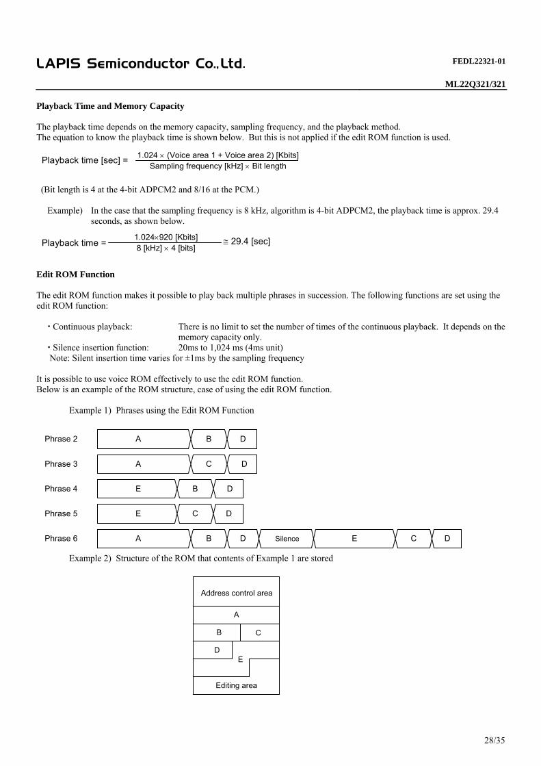
Playback Time and Memory Capacity The playback time depends on the memory capacity, sampling frequency, and the playback method. The equation to know the playback time is shown below. But this is not applied if the edit ROM function is used. (Bit length is 4 at the 4-bit ADPCM2 and 8/16 at the PCM.)
Example) In the case that the sampling frequency is 8 kHz, algorithm is 4-bit ADPCM2, the playback time is approx. 29.4 seconds, as shown below.
Edit ROM Function The edit ROM function makes it possible to play back multiple phrases in succession. The following functions are set using the edit ROM function:
Continuous playback: There is no limit to set the number of times of the continuous playback. It depends on the memory capacity only.
Silence insertion function: 20ms to 1,024 ms (4ms unit) Note: Silent insertion time varies for ±1ms by the sampling frequency
It is possible to use voice ROM effectively to use the edit ROM function. Below is an example of the ROM structure, case of using the edit ROM function.
Example 1) Phrases using the Edit ROM Function
Phrase 2
Phrase 3
Phrase 4
Phrase 5
A D
A C
E B
E C
Phrase 6
D
D
D
B
A D B E C D Silence
Example 2) Structure of the ROM that contents of Example 1 are stored
A
B C
D E
Address control area
Editing area
Playback time [sec] = 1.024 × (Voice area 1 + Voice area 2) [Kbits]
Sampling frequency [kHz] × Bit length
Playback time =
1.024×920 [Kbits] 8 [kHz] × 4 [bits]
≅ 29.4 [sec]
FEDL22321-01
ML22Q321/321
29/35
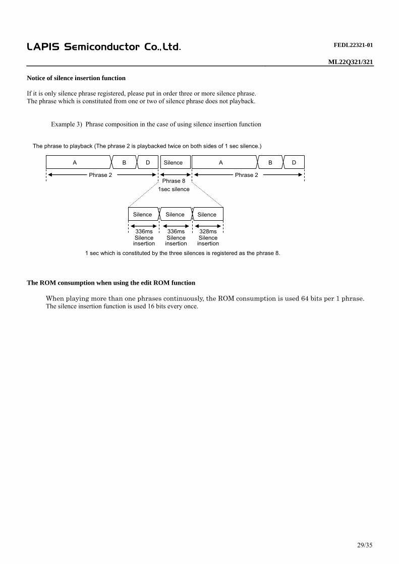
Notice of silence insertion function If it is only silence phrase registered, please put in order three or more silence phrase. The phrase which is constituted from one or two of silence phrase does not playback.
Example 3) Phrase composition in the case of using silence insertion function
The phrase to playback (The phrase 2 is playbacked twice on both sides of 1 sec silence.)
A D B
1 sec which is constituted by the three silences is registered as the phrase 8.
Silence A B D
Phrase 2 Phrase 2 Phrase 8
1sec silence
Silence
336ms Silence insertion
Silence Silence
336ms Silence insertion
328ms Silence insertion
The ROM consumption when using the edit ROM function
When playing more than one phrases continuously, the ROM consumption is used 64 bits per 1 phrase. The silence insertion function is used 16 bits every once.

FEDL22321-01
ML22Q321/321
30/35
TERMINATION OF THE VDDL PIN The VDDL pin is the regulator output that is power supply pin for the internal logic circuits. Connect a capacitor between this pin and the ground in order to prevent noise generation and power fluctuation. The recommended capacitance value is shown below. However, it is important to evaluate and decide using the own board. Also, start the next operation after each output voltage is stabilized.
Pin Recommended capacitance value Remarks
VDDL 10 µF ±20% The larger the connection capacitance, the longer the settling time.
POWER SUPPLY WIRING The power supply of this LSI is divided into the following sections:
• Digital power supply (VDD) • Analog power supply (SPVDD)
As shown below, supply the same power supply to VDD and SPVDD and separate the analog and digital power supplies by wiring.
Power supply voltage = 3 V
VDD
SPVDD
GND
SPGND
3 V
ML22321-xxx
FEDL22321-01
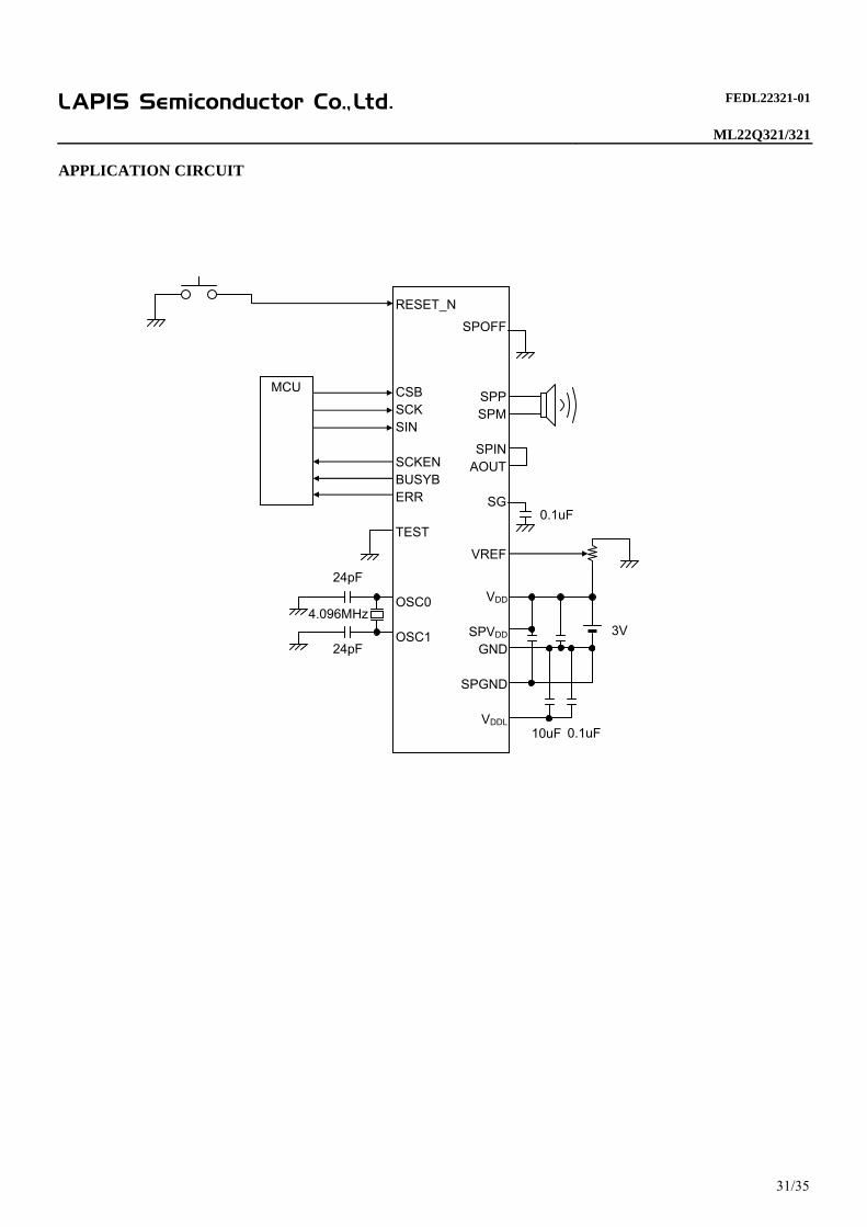
ML22Q321/321 APPLICATION CIRCUIT
SPOFF
SPPSPM
SPINAOUT
SG
VREF
RESET_N CSB SCK SIN SCKEN BUSYB ERR TEST OSC0 OSC1
4.096MHz
24pF
2
VDD
MCU
0.1uF
SPVDD
GND
SPGND
VDDL
4pF10uF 0.1uF
3V
31/35
FEDL22321-01
ML22Q321/321
32/35
PACKAGE DIMENSIONS Notes for Mounting the Surface Mount Type Package The surface mount type packages are very susceptible to heat in reflow mounting and humidity absorbed in storage. Therefore, before you perform reflow mounting, contact ROHM's responsible sales person for the product name, package name, pin number, package code and desired mounting conditions (reflow method, temperature and times). The heat resistance (example) of this LSI is shown below. Heat resistance (θJa) changes with the size and the number of layers of a substrate.
Die pad on the back of a package partial ground contact area 100%
PCB JEDEC (W/L/t=76.2/114.5/1.6(mm))
PCB Layer 4L Air cooling conditions Calm(0m/sec) Heat resistance(θJa) 45[/W]
Power consumption of Chip PMax at OutputPower 1W (5V) 0.818[W]
Power consumption of Chip PMax at OutputPower 0.5W (3.3V) 0.283[W]
TjMax of this LSI is 125. TjMax is expressed with the following formulas. TjMax = TaMax + θJa × PMax

FEDL22321-01
ML22Q321/321
33/35
Mounting area for package lead soldering to PCB (reference data) is shown below. Die pad on the back of a package should connect with the substrate of opening or a GND for heat dissipation.
Mounting area for package lead soldering to PC boards
[unit:mm]
When laying out PC boards, it is important to design the foot pattern so as to give consideration to ease of mounting, bonding,
positioning of parts, reliability, writing, and elimination of solder bridges. The optimum design for the foot pattern varies with the materials of the substrate, the sort and thickness of used soldering
paste,and the way of soldering. Therefore when laying out the foot pattern on the PC boards, refer to this figure which mean themounting area that the package leads are allowable for soldering to PC boards.
FEDL22321-01
ML22Q321/321
34/35
REVISION HISTORY
Page Document No. Date Previous
Edition CurrentEdition
Description
FEDL22321-01 Mar. 23,2015 – – Final edition 1

FEDL22321-01
ML22Q321/321
35/35
NOTES 1) The information contained herein is subject to change without notice. 2) Although LAPIS Semiconductor is continuously working to improve product reliability and quality, semiconductors can
break down and malfunction due to various factors. Therefore, in order to prevent personal injury or fire arising from failure, please take safety measures such as complying with the derating characteristics, implementing redundant and fire prevention designs, and utilizing backups and fail-safe procedures. LAPIS Semiconductor shall have no responsibility for any damages arising out of the use of our Products beyond the rating specified by LAPIS Semiconductor.
3) Examples of application circuits, circuit constants and any other information contained herein are provided only to illustrate
the standard usage and operations of the Products.The peripheral conditions must be taken into account when designing circuits for mass production.
4) The technical information specified herein is intended only to show the typical functions of the Products and examples of
application circuits for the Products. No license, expressly or implied, is granted hereby under any intellectual property rights or other rights of LAPIS Semiconductor or any third party with respect to the information contained in this document; therefore LAPIS Semiconductor shall have no responsibility whatsoever for any dispute, concerning such rights owned by third parties, arising out of the use of such technical information.
5) The Products are intended for use in general electronic equipment (i.e. AV/OA devices, communication, consumer systems,
gaming/entertainment sets) as well as the applications indicated in this document.
6) The Products specified in this document are not designed to be radiation tolerant.
7) For use of our Products in applications requiring a high degree of reliability (as exemplified below), please contact and consult with a LAPIS Semiconductor representative: transportation equipment (i.e. cars, ships, trains), primary communication equipment, traffic lights, fire/crime prevention, safety equipment, medical systems, servers, solar cells, and power transmission systems.
8) Do not use our Products in applications requiring extremely high reliability, such as aerospace equipment, nuclear power
control systems, and submarine repeaters.
9) LAPIS Semiconductor shall have no responsibility for any damages or injury arising from non-compliance with the recommended usage conditions and specifications contained herein.
10) LAPIS Semiconductor has used reasonable care to ensure the accuracy of the information contained in this document.
However, LAPIS Semiconductor does not warrant that such information is error-free and LAPIS Semiconductor shall have no responsibility for any damages arising from any inaccuracy or misprint of such information.
11) Please use the Products in accordance with any applicable environmental laws and regulations, such as the RoHS Directive.
For more details, including RoHS compatibility, please contact a ROHM sales office. LAPIS Semiconductor shall have no responsibility for any damages or losses resulting non-compliance with any applicable laws or regulations.
12) When providing our Products and technologies contained in this document to other countries, you must abide by the
procedures and provisions stipulated in all applicable export laws and regulations, including without limitation the US Export Administration Regulations and the Foreign Exchange and Foreign Trade Act.
13) This document, in part or in whole, may not be reprinted or reproduced without prior consent of LAPIS Semiconductor.
Copyright 2015 LAPIS Semiconductor Co., Ltd.
2-4-8 Shinyokohama, Kouhoku-ku,
Yokohama 222-8575, Japan http://www.lapis-semi.com/en/