ISSS wishes Happy New Year 2008! - IISc Bangaloresuresh/sukshma/sukshmaVol3No1small.pdf · PARC 4:...
8
su PARC 1: Research and Develop- ment Chair: S.B. Krupanidhi, MRC, liSe, Bangalore. PARC2: Infrastructure and human resource development Chair: Navakanta Bhat, ECE, liSe, Bangalore .• PARC 3: Aerospace applications and structuralhealth monitoring Chair: S. Gopalakrishnan, AE, liSe, Bangalore. PARC 4: Biomedical, food, and environmental applications Chair: Lazar Mathew, SBCBE, VIT, Vellore. PARC5: Automotiveapplications Chair: N.S. Vyas, ME, IIT-Kanpur. Project Director Dr. K. Vijayaraju, Aeronautical Development Agency (ADA) PB No. 1718, Vimanapura Post, Bangalore 560017 Ph: +91 (80) 25087385 Fax: +91 (80)25236146 Mobile: 0 98447 26271 emai/: vijay@jctmail.ada.gov.in Dr. K. Vijayaraju is a scientist inthe Aeronautical Development Agency (ADA), Bangalore. He can be reached at' vijay@jetmail.ada.gov.in. ISSS wishes Happy New Year 2008! INPMaSS K. Vijayaraju I With a view to harness the huge potentialof micro and smart systems technologies in our country and to equip us to reach the necessary levelof maturity, the National Programme on Smart Materials (NPSM) was launched jointly by the five scientific departmentsofthe Government oflndia, namely, DRDO, DST, CSIR, DOS and DIT in 2000 with afunding ofRs. 75 crores over a period of six years (see Vol. I. No.1, p. 1). This programme has created a pool of scientists in IITs, lISe, NITs and other leading universities with necessary experimental facilities, and has enabled twoindustries viz. BEL and SCL who took up the design, development, and prototyping ofMEMS related systesms. This has enabled the building up of basic infrastructure for many of these technologies, design,and development of basic devices (e.g., pressuresensors, accelerometers, patch antenna, RF devices), materials, and processes.Creating an awareness amongst our scientific community was alsoamajor accomplishment of this programme. An- other important outcome of this programme has been the realizationby the industries to adopt these technologies to keep their market edge. It is imperative now that this all-pervasive technologyshould be progressed further to build a variety of productsand subsystems, which are of importance to both defence and civilian sectors. It is with this in mind that a National Programme on Micro and Smart Systems(NPMaSS)jointly by the same five departments was proposed. The lead was takenby Dr. Y.K. Aatre, former SA to RM and Former Secretary, Defence, R&D and presently a Visiting Professor, ECE Department, lISe, in formulating a proposal for the national programme and submitting the same to the government for approval. The NPMaSS has now been sanctionedby the government with a budget ofRs. 195 crores spread over five years from September 2007. As mentioned earlier, it is a joint programme of the same fivescientific departments ofthe government, namely, DRDO, DOS, DST, MIT, and CSIR. The programme isfunded by DRDO and run through Aeronautical Development Agency (ADA), Bangalore. Programme objectives: The main objective of the NPMaSS is to consolidate the gains from NPSM through the realization of products/devices/subsystems based on MEMS and smart materials technology, and their field demonstration. Various developments thus undertaken would aim tosupport applications in aerospace and defence areas, and to achieve commercial exploitation in the automotive, biomedical, environmental safety and fooo technology related sectors and in the health-monitoring of infrastructure in the civilian sector. Under this programme a component/system level characterization facility would be established to act as an interface between the developer and the user for speedy implementation of the developed devices. This programme will liaise with industries in various sectors identified and to give a major thrust in achieving significant humanresource development in this important area of advanced technology. It isa'directed programme' in the sense that projects tailoredto meet the programme objectives will besought and sanctionedto institutions having necessary expertise and facilities. Programme management structure: The Programme has a three-tier management structure as follows: (i)Smart Apex Board (SAB),lays down the overallpolicy guidelines. The Board is headed by SA to RM, Secretary, Dept. of Defence Research and Development, Ministry of Defence, as itschairman. (ii) Board for Smart Materials Research and Technology (B-SMART) has the executiveand financial authority of implementing theprogramme. It is headed by Dr. Y.K. Aatre as chairman at the request of SAB. Project Director ofNPMaSS is its member-secretary. (iii) Project Assessment and Review Committees (PARCs) to execute the technicalpartofthe programme (i.e., seeking and receiving, assessing and recommending, monitoring and reviewing all the projects in the specified sub-area) as per the guidelines from SAB and action plans recommended by B-SMART. A Programme Cell at ADA, headed by a Project Director (NPMaSS) is responsible for the overall execution of the Programme as per the directives from B-SMART. Dr. K. Vijayaraju from ADA, Bangalore, has been designated as the Project Director. Programme implementation The B-SMART has identified five Project Assessment and Review Committees (PARCs) with aspecific focus area and chairman to coordinate the activities for each of them. Focusarea for each PARCwith the respective chairman are also appointed (see the tableon the left). *
Transcript of ISSS wishes Happy New Year 2008! - IISc Bangaloresuresh/sukshma/sukshmaVol3No1small.pdf · PARC 4:...

su
PARC 1: Research and Develop-mentChair: S.B. Krupanidhi, MRC, liSe,Bangalore.
PARC 2: Infrastructure and humanresource developmentChair: Navakanta Bhat, ECE, liSe,Bangalore .•
PARC 3: Aerospace applicationsand structural health monitoringChair: S. Gopalakrishnan, AE,liSe, Bangalore.
PARC 4: Biomedical, food, andenvironmental applicationsChair: Lazar Mathew, SBCBE, VIT,Vellore.
PARC 5: Automotive applicationsChair: N.S. Vyas, ME, IIT-Kanpur.
Project DirectorDr. K. Vijayaraju,Aeronautical DevelopmentAgency (ADA)PB No. 1718, VimanapuraPost, Bangalore 560017Ph: +91 (80) 25087385Fax: +91 (80)25236146Mobile: 0 98447 26271emai/:[email protected]
Dr. K. Vijayaraju is a scientistin the AeronauticalDevelopment Agency (ADA),Bangalore. He can bereached at'[email protected].
ISSS wishes Happy New Year 2008!INPMaSS K. Vijayaraju IWith a view to harness the huge potential of micro and smart systems technologies in our country and toequip us to reach the necessary level of maturity, the National Programme on Smart Materials (NPSM)was launched jointly by the five scientific departments ofthe Government oflndia, namely, DRDO, DST,CSIR, DOS and DIT in 2000 with a funding ofRs. 75 crores over a period of six years (see Vol. I. No.1, p.1). This programme has created a pool of scientists in IITs, lISe, NITs and other leading universities withnecessary experimental facilities, and has enabled two industries viz. BEL and SCL who took up thedesign, development, and prototyping ofMEMS related systesms. This has enabled the building up ofbasic infrastructure for many of these technologies, design, and development of basic devices (e.g.,pressure sensors, accelerometers, patch antenna, RF devices), materials, and processes. Creating anawareness amongst our scientific community was also a major accomplishment of this programme. An-other important outcome of this programme has been the realization by the industries to adopt thesetechnologies to keep their market edge.
It is imperative now that this all-pervasive technology should be progressed further to build a variety ofproducts and subsystems, which are of importance to both defence and civilian sectors. It is with thisin mind that a National Programme on Micro and Smart Systems (NPMaSS)jointly by the same fivedepartments was proposed. The lead was taken by Dr. Y.K. Aatre, former SA to RM and FormerSecretary, Defence, R&D and presently a Visiting Professor, ECE Department, lISe, in formulating aproposal for the national programme and submitting the same to the government for approval. TheNPMaSS has now been sanctioned by the government with a budget ofRs. 195 crores spread over fiveyears from September 2007. As mentioned earlier, it is a joint programme of the same five scientificdepartments ofthe government, namely, DRDO, DOS, DST, MIT, and CSIR. The programme is fundedby DRDO and run through Aeronautical Development Agency (ADA), Bangalore.
Programme objectives: The main objective of the NPMaSS is to consolidate the gains from NPSMthrough the realization of products/devices/subsystems based on MEMS and smart materials technology,and their field demonstration. Various developments thus undertaken would aim to support applicationsin aerospace and defence areas, and to achieve commercial exploitation in the automotive, biomedical,environmental safety and fooo technology related sectors and in the health-monitoring of infrastructurein the civilian sector. Under this programme a component/system level characterization facility would beestablished to act as an interface between the developer and the user for speedy implementation of thedeveloped devices. This programme will liaise with industries in various sectors identified and to givea major thrust in achieving significant human resource development in this important area of advancedtechnology. It is a 'directed programme' in the sense that projects tailored to meet the programmeobjectives will be sought and sanctioned to institutions having necessary expertise and facilities.
Programme management structure: The Programme has a three-tier management structure as follows:
(i) Smart Apex Board (SAB), lays down the overall policy guidelines. The Board is headed by SA toRM, Secretary, Dept. of Defence Research and Development, Ministry of Defence, as its chairman.
(ii) Board for Smart Materials Research and Technology (B-SMART) has the executive and financialauthority of implementing the programme. It is headed by Dr. Y.K. Aatre as chairman at the request ofSAB. Project Director ofNPMaSS is its member-secretary.
(iii) Project Assessment and Review Committees (PARCs) to execute the technical part ofthe programme(i.e., seeking and receiving, assessing and recommending, monitoring and reviewing all the projects inthe specified sub-area) as per the guidelines from SAB and action plans recommended by B-SMART.
A Programme Cell at ADA, headed by a Project Director (NPMaSS) is responsible for the overall executionof the Programme as per the directives from B-SMART. Dr. K. Vijayaraju from ADA, Bangalore, has beendesignated as the Project Director.
Programme implementation
The B-SMART has identified five Project Assessment and Review Committees (PARCs) with a specificfocus area and chairman to coordinate the activities for each of them. Focus area for each PARC with therespective chairman are also appointed (see the table on the left). *

Fifth ISSS International Conference onSmart aterials. Structures and Systems
24 - 26 July 2008• Adaptive materials• Sensors and actuators• Design, modeling and simulation• MEMS design, electronics and packaging• Nanotechnologies• Signal processing techniques• Applications
National Science Seminar ComplexIndian Institute of Science
Bangalore. INDIA
Dates to NoteLast date for submission of abstract:February 15, 2008
Receipt of the full paper for review: March15,2008
Acceptance of the full paper after review:May 7,2008
Deadline for receipt of the revised full paper:June 7, 2008
Last date for advance registration: June 15,2008
IThe abstract should be around 500 - 800 words. The abstract should be sent in MS Word, Postscript orIPDF format. The abstracts should be [email protected] as to reach on or before February 15, 2008.
I-sss News
The 2nd ISSS National Conference on MEMS, Microsensors, Smart Materials, Structures and Systems took place on 16th and 17th,
November, 2007, in Pilani. This conference was jointly organized by the Central Electronics Engineering Research Institute (CEERI) andthe Birla Institute of Technology and Science (BITS) on the CEERI campus. Several ofthe attendees were ISSS members. The number ofpapers fH"esentedin this conference has risen significantly as compared with the first ISSS national conference held in 2006 in ResearchCentre lmarat (RCI), Hyderabad. This shows that the efforts of ISSS and those of others in promoting research in the micro and smartsystems are bearing fruits. In this conference ten invited speakers delivered talks on various cutting-edge topics. There were about 70oral presentations and more than 40 poster presentations. The dignitaries in the inaugural function included the heads of the organizinginstitutions, Dr. Chandra Shekhar, Director-CEERI and Prof. LX. Maheswari, Vice-Chancellor, BITs; ISSS President Dr. A.R. Upadhya,;Dr. T. Ramasami, Secretary, DST; Prof. Y.K. Aatre, Former Scientific Advisor to Raksha Mantri, and others. Prof. LX. Maheswari of BITSwelcomed the attendees and Dr. Y.K. Dwivedi gave the vote of thanks. On the second day of the conference, ISSS honored Prof. A.Selvarajan and Dr. Vikram KumaI' for their contributions to the growth of their respective fields. The conference was well attended byacademics including faculty and students, researchers from government organizations, and participants from the industry. The conferencewas organized very well for which the organizing institutions are to be congratulated. *
__ E_d_i_t_o_r_ia_I_~_e_a_m__ II~ IS_S_S__ E_x_e_c_u_t_i_v_e_C_o_u_n_c_il _G.K. Ananthasuresh, IISc (Editor)S. Gopalakrishnan, IIScJ. Gurudutt, BigtecG.M. Kamath, NALK.J. Vinoy, IISc
Art Design: G. Bharathi
President: A.R. Upadhya Vice-president: P.O. MangalgiriSecretaries: S. Gopalakrishnan and K. Vijayaraju Treasurer: G.M. Kamath
Members: s. Mohan, J. Gurudult, G.K. Ananthasuresh, and the presidents of Hyderabad and Delhi chapter.
This newsletter is sent to allISSSmembers by postal mail.
To become an ISSS member, downloadhttp://www.isss.org.in/membership.htm Iand send the form with payment to:Institute of Smart Structures and SystemsDepartment of Aerospace EngineeringIndian Institute of Science, Bangalore560012, India
ISSS admission fee: Rs. 200Member:
Rs. 200 (annual); Rs. 2,000 (life)Student member:Rs. 75 (annual)
Corporate member:Rs. 10,000 (annual); Rs. 50,000 (life)
Payable to "ISSS, Bangalore".

Microelectromcchanical Systems (MEMS) based applications are part of an emerging market in India while somc otherparts of the world have established this technology with a very high growth rate. To help India initiate a major effort inestablishing a MEMS market, Bharat Electronics Limited was actively involved in the National programme on SmartMaterials ( PSM, see Vol. I, No. I, p. I). The Bangalore Components Division of BEL got a grant from NPSM to the tune
. ofRs. 10 crores for the establishment of wafer-level MEMS processing·capabilities. The major equipments obtained bythis programme are a double-side mask aligner, an anodic bonder, a flip-chip bonder, a reactive ion etcher, and a networkanalyser. Using these, the basic technology development included bulk micromachining for the pressure sensor, surfacemicromachining for an RF switch, and wafer-level packaging for RF MEMS (see Vol. 2, No.2, pp. 4-5) components. A separate class 100 cleanroom facility was established in the Silicon Building at Bangalore complex to house these facilities. The basic R & 0 activity started after theinstallation of this facility around 2004 to take up focused product development. The MEMS group has successfully developed theprototypes of (i) a low profile integrated pressure sensor for Light Combat Aircraft (LCA) applications, (ii) a force-balance accelerometer forstrategic applications, (iii) LPG gas sensor chip based on silicon nitride and polysilicon technology, (iv) an SOl Technology for pressure
sensors, and (v) medium pressure sensors for tire inflatorapplications up to lObar. The MEMS group is interactingwith lISc, DRDL, RCI, and IITs to get the R & D supportfor the design and process development. It was closelyinteracting with lIT-Madras to dcvelop accelerometerand pressure sensors. Prof. K.N. Bhat was guiding theBEL MEMS team as a part of the NPSM programme.With the experience gained from NPSM activities andinteraction with national/international experts, a focusedproduct oriented development programme has beendrawn up as shown in Fig. I. More details about BEL'sMEMS activities and an educational pressure sensor kitdeveloped by BEL are given in pages 4-5.
ILeaders of ISSS: Kola Harinarayana
Dr. K. Natarajan is theAdditional General Manager.MEMS at BEL, Bangalore. Hecan be reached [email protected].
Dr. Kota Ilarinarayana is a distinguished scientist and an outstanding engineer. He was the former ProgrammeDirector of the Light Combat Aircraft (LCA) project and the Vice Chancellor of Central University ofHyderabad. Hewas bom in Berhampur, Orissa, in 1943, graduated from Benaras Hindu University (BHU) in mechanical engineering,and obtained a mastcrs degree in aerospace engineering from IISc, Bangalore. He did his PhD in lIT-Mumbai, andalso holds a bachelors degree in law.
Dr. Kota Harinarayana startcd his career in 1967 at HindustanAeronautics Ltd. (HAL), Bangalore. He moved to thcDefence Rcsearch Development Organisation (DRDO), Government of India head quarters in 1970 and stayedthere until 1982 holding various positions. He rejoined HAL in 1982 as the Chief Designer in Nasik Division. He was deputed to DRDO in1985 and assumed charge as Director, ADE, Bangalore. He was appointed LCA Programme Director in December 1985 and he wasconcurrently holding the post of Director, ADE, till 1986. During 1995 he was elevated as a Distinguished Scientist by DRDO. AsProgrammc Director and Chief Designer of LCA, he successfully directed the project leading to flight-testing and clearancc for limitedseries production. Thanks to his efforts, India succeeded in developing a state-of-the-art, high-technology fighter aircraft of the worldclass. Dr. Harinarayana played a key role in life extension and determination of components of the MiG 21 aircraft, and indigcnisation ofcomponcnts, spares, and consumables of aircraft during his tenure as the Chief Resident Engineer, Nasik. New aerodynamic dcvice vortexplate was fl ight-tested on a MiG 21 aircraft for the first time in the world. He is currently the Raja Ramanna Fellow at the National AerospaceLaboratorics (NAL) and is pursuing his vision of developing an indigenous 70-seater passenger aircraft for India.
As thc formcr programmc director ofLCA at ADA, he worked actively for the creation of National Programme on Smart Materials (NPSM),which was the nodal agcncy for implementing this programme. He headed a committee, which drew up the specifications for various smartmaterials, sensors and dcvices for various applications. His committee report formed the basis for all the devices and matcrials developedunder NPSM (see Vol. I, No. I, p. I)
Dr. Harinarayana also served as the President, Aeronautical Society oflndia; Chairman, Technical Committee of ARDB; Fellow, AeronauticalSociety oflndia and Indian Academy of Engineering. He received distinguished alumnus award from aerospace department, IISc, Bangalorein 1993 and from liT-Bombay in 1995. He is the recipient ofthe National Aeronautics Prize, FIE Foundation Award-1996 and SB1-PragnaPliraskar-]O() I. He rcceived the Dr. Y. Nayudamma Memorial Award for 200 I. He received the DRDO Technology Leadership Award for200 I. lIe was honoured with Padma Shri by the Government of India in 2002.
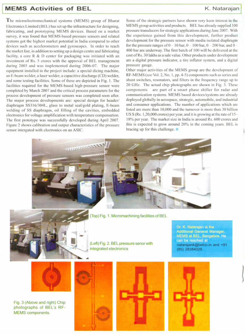
The microelectromechanical systems (MEMS) group of BharatElectronics Limited (BEL) has set up the infrastructure for designing,fabricating, and prototyping MEMS devices. Based on a marketsurvey, it was found that MEMS-based pressure sensors and relatedsystems got the highest market potential in India compared to otherdevices such as accelerometers and gyroscopes. In order to reachthe market fast, in addition to setting up a design centre and fabricatingfacility, a core R & D center for packaging was initiated with aninvestment of Rs. 5 crores with the approval of BEL managementduring 2005 and was implemented during 2006-07. The majorequipment installed in the project inelude: a special dicing machine,an E-beam welder, a laser welder, a capacitive discharge (CD) welder,and some testing facilities. Some of these are depicted in Fig. I. Thefacilities required for the MEMS-based high-pressure sensor werecompleted by March 2007 and the critical process parameters for theprocess development of pressure sensors was completed soon after.The major process developments are: special design for header/diaphragm SS3161304L, glass to metal seal/gold plating, E-beamwelding of SS diaphragm, oil filling of the cavities, embeddedelectronics for voltage amplification with temperature compensation.The first prototype was successfully developed during April 2007.Figure 2 shows calibration and output characteristics of the pressuresensor intergated with electronics on an ASIC.
K. Natarajan ISome of the strategic partners have shown very keen interest in theMEMS group activities and products. BEL has already supplied 100pressure transducers for strategic applications during June 2007. Withthe experience gained from this development, further productdevelopment for the pressure sensor with media isolated diaphragmfor the pressure ranges of 0 - lObar, 0 - 100 bar, 0 - 200 bar, and 0 -400 bar are underway. The first batch of 100 will be delivered at thecost ofRs. 30 lakhs as a sale value. Other products under developmentare a digital pressure indicator, a tire inflator system, and a digitalpressure gauge.Other major activities of the MEMS group are the development ofRF-MEMS (see Vol. 2, No.1, pp. 4-5) components such as series andshunt switches, resonators, and filters in the frequency range up to20 GHz. The actual chip photographs are shown in Fig. 3. Thesecomponents are part of a smart phase shifter for radar andcommunication systems. MEMS based devices/systems are alreadydeployed globally in aerospace, strategic, automobile, and industrialand consumer applications. The number of applications which arelisted are more than 10,000 and the turnover is more than 30 billionUS $ (Rs. 1,20,000 crores) per year, and it is growing at the rate of 15-18% per year. The market size in India is around Rs. 600 crores andthis is expected to grow around 20% in the coming years. BEL isbracing up for this challenge.
(Left) Fig. 2. BEL pressure senor withintegrated electronics
Fig. 3 (Above and right) Chipphotographs of BEL's RF-MEMS components.
[email protected] and +91(80) 28384028.

The MEMS group of Bharat Electronics Limited (BEL) has designed and built a ·pressure sensor college kie to enablecollege and university students understand and appreciate micromachined sensor technology. The picture ofthe kit and itscontents are shown below. A number of experiments can be performed using this kit. The includes many accessories asindicated below. Thus, the students will be able to perform the experiment in the laboratory of a typical engineering college.Those interested in this kit may contact the author of this article.
Pressure sensorcollege kit
1 bar TO-8 sensors (#2)2 bar TO-8 sensors (#2)10 bar TO-8 sensors (#2)
Nozzle for TO-8 sensor (#1)Compensated sensor (# I)Nozzle for compensated sensor (# I)Bulk micromachined Siwafer (# I)
Test jig (# 1)Digital pressure indicator (#1)
PVC hose pipe (2 m long)User's manualMEMS product information
Possible experiments with the pressure sensor college kit* Characterization of the uncompensated pressure sensors to understand parameters such as offset, span, linearity, etc.* A study of the effect of temperature and pressure to obtain the temperature coefficient of the offset, span, etc.* Studying the methods of compensation for adapting the uncompensated sensors for compensated output.* Comparing the ASIC compensated pressure sensor, which can be characterized with two temperatures and different pressures,with the one compensated in the lab.* A study to distinguish between gauge and absolute types of pressure sensors.
A silicon wafer with bulk-micromachined pressure sensor diaphragms helps the student understand how the mechanical elementof the pressure sensor is made and it gives an idea of the size of the sensor element. By testing the uncompensated pressuresensors, students can appreciate the effect of temperature on the output. This output is a few mV as can be seen in Fig. 1. Thevariation seen in Fig. 1 is due to the temperature coefficient of the piezoresisters in the sensor. An ASIC included with thecompensated pressure sensor of the kit not only adjusts for temperature variations but also amplifies the output to 0-5 V range(see Fig. 2). The digital pressure indicator enables viewing the pressure reading directly in pressure units rather than as avoltage. The LCD display on the indicator has the provision to show the pressure in psi, kPa, or bar. *
120100
~80
5 60a-S 400
20
00 20 40 60
5.000- 4.000-+-O'C ~- 3.000~Room ::sSo
Temp. ::s 2.000-Ir-5O'C Q
~ 1.000~~8O'C =- 0.000-Q
>
Pressure(PSI)
Fig. 1. Uncompensated "raw" sensor
-oc-25C
SOC

D. Kauri
~ Shape Memory Alloy (SMA; see Vol. 2, No.3, pp. 4-5) thin film has been recognized as a promising and high-performancematerial for microelectromechanical systems (MEMS) applications because it can be patterned with standard lithography
techniques and can be fabricated in a batch process mode. The phase transformation in SMA thin film is accompanied by significantchanges in the mechanical, physical, chemical, electrical, and optical properties. These changes can be exploited in the design andfabrication of microsensors and microactuators. The Nanostructured Thin Film Research Lab at the Indian Institute of Technology-Roorkee (lIT-Roorkee) is actively involved in the fabrication of high-quality titanium-nickel (TiNi) shape memory thin fiIms and heterostructuresfor MEMS applications. Proper passivation to prevent surface layer degradation and nickel releasing into the environment has beenconsidered crucial for the medical applications of TiNi based shape memory alloys. The surface properties and corrosion resistance areimportant material characteristics that enable the use ofTiNi for surgical devices in the human body. Therefore, a stable, biocompatible andcorrosion resistant passive layer is required. The present research at lIT Roorkee deals with the deposition and the effect of nanocrystallineTiNi protective layer on TiNi thin films prepared by dc magnetron sputtering (see Fig. 1) to improve the surface properties and thebiocompatibility of SMA thin films. The goal of this research is to investigate the influence of the size and preferred orientation of grainsin the passivation layer on the mechanical, chemical and functional properties of TiN/TiNi heterostructure and to investigate the criticalthickness of passivation layer up to which shape memory properties can be retained.
The group is also involved in the synthesis of nanostructured materials by physical vapour deposition (PVD) processes such as RF/DCmagnetron sputtering system with the facility to deposit nanocrystalline powder, thin films, and multi layers by varying the substratetemperature from -150°C to 850°C with a base pressure of about 10-8 Torr and multi-chamber Excimer based pulsed laser deposition (PLD, Lambda Physik, KrF; see Fig. 2) formulti layers and heterostructures of functional nanomaterials. A number of other newresearch projects have been taken up by this group. The notable ongoing research projectsinclude Functional Nanocomposites: Synthesis, Characterization & Applications (DST,India), Functional Nanostructures for MEMS & Optoelectronic devices (DIT, India), andDevelopment of Super-hard Nanocomposite Coatings (DRDO, India). *
Dr. Davinder Kaur is an AssistantProfessor it) the Physics Departmentof IIT-Roorkee. She can be reached [email protected].
"The MEMS INNOVATION FEST 2007 was organized by Step Electronics Pvt.Ltd. along with Karnataka Hybrid Micro Devices Ltd., & Jain Group of Institu-tions at the Central Power Research Institute (CPRI), Bangalore, on 9th & 10thDec 2007.The conference focused on bridging the gap between design and product throughinnovation, which was well-received and appreciated by the participants. TheMEMS conferences held in India thus far focused on sensitising the academiccommunity. The theme of the MEMS Innovation Fest falls beyond the aca-demic realm and hence was organised focusing on industrial community.It was interesting to note that the participation was from all the quarters ofacademics, industries, and government sectors. There were more than 25 pa-pers presented covering micro sensors and actuators, RF MEMS, energy har-vesting using MEMS as well as MEMS in agriculture. The technical sessionswere well attended. Participants benefited from the MEMS course conductedby Prof, Chengkuo Lee Vincent of IME - A*STAR, National University ofSingapore." (Contributed by V. Janardhan and S. Pamidighantam)
A recent article in Applied PhysicsLetters (91, 201902, 2007) by S.Bhowmik et aI., reports that bulksilicon is susceptible to cyclic fa-tigue. It was a matter of debatebecause no evidence was reportedearlier. The experiment that pro-vided this counter evidence to theestablished theory involved inden-tation of a bulk silicon surface withmicro spheres. The paper presentsthe details and discusses its pos-sible inmplications in siUcon basedmicro devices.

I Accomplishments: NAL (Part 2 of 2)
The first of this two-part article focused onthe materials research and MEMS devicedevelopment being carried out in NationalAerospace Laboratories (NAL), India's pre-mier civilian laboratory for aeronautical andaerospace R&D (website: www.nal.res.in).The aerospace applications research usingsmart materials are covered in this secondand concluding part.
Shape Memory Alloy (SMA) Applications:The important achievements in the SMAapplications area ~elate to exploiting thebasic material properties (both thermal andstress induced) of NiTi SMA (see Vol. l,No.3, pp. 4-5) for aerodynamic morphing(shape change). Conventional aircraftcontrol surfaces such as flap (which aremovable) are housed in fixed lifting surfacessuch as wing. The smart SMA based controlsurface has no distinct moving parts as theentire lifting surface can be made to undergoshape changes. This works like the wing ofa bird, which generates the required controlforce by flexing the wing appropriately.Towards this goal, a smart control surfacewas built incorporating SMA elements(Fig. I). The model has been successfullytested in the wind tunnel up to a maximumspeed of 160 km/hr. Successful SMAapplications have also been evolved in NALfor innovative SMA-based repairtechno logics and energy absorptionmechanisms.
Vibration and Aeroelastic Applications:Aircraft structures are susceptible tovibration due to the nature of the air flowaround them. Moreover, the coupling ofthestructural vibration with the aerodynamicforces often results in undesirablephenomena termed as aeroelasticinstabilities. One way to mitigate theseproblems is to use active control techniquesusing smart actuators. A successful windtunnel demonstration of active fluttercontrol technology on a composite wingusing a trailing edge flap acting as anaerodynamic effector has beendemonstrated at NAL. NAL has alsodesigned, developed, and successfullytested amplifiable piezo mechanisms forstructural control applications. Thenecessary in-flight electronics has alsobeen developed. A laboratory leveldemonstration of vibration controlexperiment using distributed PZT stacks ona composite T-Tail structure has beenplanned under the simulated aircraft powerenvironment (Fig. 2). Vibration control offull scale fin-tip structure of LCA has beenachieved using a system built aroundTexas Instruments 6711 floating point DigitalSignal Processor board in a Pentium 4 hostPc. The control law implemented in C++ is
Fig. 1. Adaptive control surface usingSMA actuators.
G.M. Kamath I
Fig. 3. A composite structure with embedded fibre optic sensors for healthmonitoring.
based on the well known computationallyefficient & simple Filtered - X Least MeanSquare(LMS) algorithm. The controlactuators can be PZT patches, bimorphsor stacks. Sensing is by PZT patches oraccelerometers.
Structural Health Monitoring: Healthmonitoring of aircraft is gaining increasingimportance due to significant cost benefits.The cost benefits accrue by dispensingwith routine maintenance and inspections,and replacing with a 'maintenance-on-demand' concept. Efforts at NAL havebeen to develop the necessary system tomonitor the health of a typical aircraftcomposite structure using fibre opticsensors. Towards this end, the technologyfor embedding Fibre Bragg Orating (FBO)sensors (see Vol. 1, NO.1, pp. 4-5) intocomposite structures has been developed,and study of associated issues, includingsensor characterization, certificationrequirements, etc., have been done.Constant upgradation of the requisiteinstrumentation and software for data
acquisition, processing and interpretationof sensor data is also being done. Thedesign, fabrication and testing of typicalcomposite structures to study the effectof damages on static strain patterns havebeen carried out (Fig. 3). These structureswere also used to validate the SHMmethodology developed. An SHMmethodology based on artificial neuralnetworks has been developed for loadmonitoring and damage detection. Thefocus now is on developing systems thatcan be flight tested on an aircraft. Theplatforms currently being studied are theUnmanned Aerial Vehicle, Nishant, theLight Combat Aircraft, Tejas, and the LightTransport Aircraft, SARAS. *
The author, G.M. Kamath who is ascientist in NAL, acknowledges theinputs of his colleagues for thisarticle. Oversights, if any, are that ofthe author. Queries may please besent to [email protected].

SUKSH.MAInstitute of Smart Structures and SystemsDepartment of Aerospace EngineeringIndian Institute of ScienceBangalore - 560012India