ispMACH 4000ZE Family - Home - Lattice Semiconductor/media/LatticeSemi/Documents...ispMACH 4000ZE...
60
www.latticesemi.com 1 DS1022_01.7 ispMACH 4000ZE Family 1.8V In-System Programmable Ultra Low Power PLDs February 2012 Data Sheet DS1022 ® © 2012 Lattice Semiconductor Corp. All Lattice trademarks, registered trademarks, patents, and disclaimers are as listed at www.latticesemi.com/legal. All other brand or product names are trademarks or registered trademarks of their respective holders. The specifications and information herein are subject to change without notice. Features High Performance •f MAX = 260MHz maximum operating frequency •t PD = 4.4ns propagation delay • Up to four global clock pins with programmable clock polarity control • Up to 80 PTs per output Ease of Design • Flexible CPLD macrocells with individual clock, reset, preset and clock enable controls • Up to four global OE controls • Individual local OE control per I/O pin • Excellent First-Time-Fit TM and refit • Wide input gating (36 input logic blocks) for fast counters, state machines and address decoders Ultra Low Power • Standby current as low as 10μA typical • 1.8V core; low dynamic power • Operational down to 1.6V V CC • Superior solution for power sensitive consumer applications • Per pin pull-up, pull-down or bus keeper control* • Power Guard with multiple enable signals* Broad Device Offering • 32 to 256 macrocells • Multiple temperature range support – Commercial: 0 to 90°C junction (T j ) – Industrial: -40 to 105°C junction (T j ) • Space-saving ucBGA and csBGA packages* Easy System Integration • Operation with 3.3V, 2.5V, 1.8V or 1.5V LVCMOS I/O • 5V tolerant I/O for LVCMOS 3.3, LVTTL, and PCI interfaces • Hot-socketing support • Open-drain output option • Programmable output slew rate • 3.3V PCI compatible • I/O pins with fast setup path • Input hysteresis* • 1.8V core power supply • IEEE 1149.1 boundary scan testable • IEEE 1532 ISC compliant • 1.8V In-System Programmable (ISP™) using Boundary Scan Test Access Port (TAP) • Pb-free package options (only) • On-chip user oscillator and timer* *New enhanced features over original ispMACH 4000Z Table 1. ispMACH 4000ZE Family Selection Guide ispMACH 4032ZE ispMACH 4064ZE ispMACH 4128ZE ispMACH 4256ZE Macrocells 32 64 128 256 t PD (ns) 4.4 4.7 5.8 5.8 t S (ns) 2.2 2.5 2.9 2.9 t CO (ns) 3.0 3.2 3.8 3.8 f MAX (MHz) 260 241 200 200 Supply Voltages (V) 1.8V 1.8V 1.8V 1.8V Packages 1 (I/O + Dedicated Inputs) 48-Pin TQFP (7 x 7mm) 32+4 32+4 64-Ball csBGA (5 x 5mm) 32+4 48+4 64-Ball ucBGA (4 x 4mm) 48+4 100-Pin TQFP (14 x 14mm) 64+10 64+10 64+10 132-Ball ucBGA (6 x 6mm) 96+4 144-Pin TQFP (20 x 20mm) 96+4 96+14 144-Ball csBGA (7 x 7mm) 64+10 96+4 108+4 1. Pb-free only.
Transcript of ispMACH 4000ZE Family - Home - Lattice Semiconductor/media/LatticeSemi/Documents...ispMACH 4000ZE...
www.latticesemi.com 1 DS1022_01.7
ispMACH 4000ZE Family1.8V In-System Programmable
Ultra Low Power PLDsFebruary 2012 Data Sheet DS1022
®
© 2012 Lattice Semiconductor Corp. All Lattice trademarks, registered trademarks, patents, and disclaimers are as listed at www.latticesemi.com/legal. All other brandor product names are trademarks or registered trademarks of their respective holders. The specifications and information herein are subject to change without notice.
Features High Performance
• fMAX = 260MHz maximum operating frequency• tPD = 4.4ns propagation delay • Up to four global clock pins with programmable
clock polarity control• Up to 80 PTs per output
Ease of Design• Flexible CPLD macrocells with individual clock,
reset, preset and clock enable controls• Up to four global OE controls• Individual local OE control per I/O pin• Excellent First-Time-FitTM and refit• Wide input gating (36 input logic blocks) for fast
counters, state machines and address decoders
Ultra Low Power• Standby current as low as 10µA typical• 1.8V core; low dynamic power• Operational down to 1.6V VCC• Superior solution for power sensitive consumer
applications• Per pin pull-up, pull-down or bus keeper
control*• Power Guard with multiple enable signals*
Broad Device Offering• 32 to 256 macrocells• Multiple temperature range support
– Commercial: 0 to 90°C junction (Tj)– Industrial: -40 to 105°C junction (Tj)
• Space-saving ucBGA and csBGA packages*
Easy System Integration• Operation with 3.3V, 2.5V, 1.8V or 1.5V
LVCMOS I/O• 5V tolerant I/O for LVCMOS 3.3, LVTTL, and PCI
interfaces• Hot-socketing support• Open-drain output option• Programmable output slew rate• 3.3V PCI compatible• I/O pins with fast setup path • Input hysteresis*• 1.8V core power supply• IEEE 1149.1 boundary scan testable• IEEE 1532 ISC compliant• 1.8V In-System Programmable (ISP™) using
Boundary Scan Test Access Port (TAP)• Pb-free package options (only)• On-chip user oscillator and timer*
*New enhanced features over original ispMACH 4000Z
Table 1. ispMACH 4000ZE Family Selection Guide
ispMACH 4032ZE ispMACH 4064ZE ispMACH 4128ZE ispMACH 4256ZE
Macrocells 32 64 128 256
tPD (ns) 4.4 4.7 5.8 5.8
tS (ns) 2.2 2.5 2.9 2.9
tCO (ns) 3.0 3.2 3.8 3.8
fMAX (MHz) 260 241 200 200
Supply Voltages (V) 1.8V 1.8V 1.8V 1.8V
Packages1 (I/O + Dedicated Inputs)
48-Pin TQFP (7 x 7mm) 32+4 32+4
64-Ball csBGA (5 x 5mm) 32+4 48+4
64-Ball ucBGA (4 x 4mm) 48+4
100-Pin TQFP (14 x 14mm) 64+10 64+10 64+10
132-Ball ucBGA (6 x 6mm) 96+4
144-Pin TQFP (20 x 20mm) 96+4 96+14
144-Ball csBGA (7 x 7mm) 64+10 96+4 108+4
1. Pb-free only.
ispMACH 4000ZE Family Data Sheet
2
IntroductionThe high performance ispMACH 4000ZE family from Lattice offers an ultra low power CPLD solution. The new fam-ily is based on Lattice’s industry-leading ispMACH 4000 architecture. Retaining the best of the previous generation,the ispMACH 4000ZE architecture focuses on significant innovations to combine high performance with low powerin a flexible CPLD family. For example, the family’s new Power Guard feature minimizes dynamic power consump-tion by preventing internal logic toggling due to unnecessary I/O pin activity.
The ispMACH 4000ZE combines high speed and low power with the flexibility needed for ease of design. With itsrobust Global Routing Pool and Output Routing Pool, this family delivers excellent First-Time-Fit, timing predictabil-ity, routing, pin-out retention and density migration.
The ispMACH 4000ZE family offers densities ranging from 32 to 256 macrocells. There are multiple density-I/Ocombinations in Thin Quad Flat Pack (TQFP), Chip Scale BGA (csBGA), and Ultra Chip Scale BGA (ucBGA) pack-ages ranging from 32 to 144 pins/balls. Table 1 shows the macrocell, package and I/O options, along with other keyparameters.
A user programmable internal oscillator and a timer are included in the device for tasks like LED control, keyboardscanner and similar housekeeping type state machines. This feature can be optionally disabled to save power.
The ispMACH 4000ZE family has enhanced system integration capabilities. It supports a 1.8V supply voltage and3.3V, 2.5V, 1.8V and 1.5V interface voltages. Additionally, inputs can be safely driven up to 5.5V when an I/O bankis configured for 3.3V operation, making this family 5V tolerant. The ispMACH 4000ZE also offers enhanced I/Ofeatures such as slew rate control, PCI compatibility, bus-keeper latches, pull-up resistors, pull-down resistors,open drain outputs and hot socketing. Pull-up, pull-down and bus-keeper features are controllable on a “per-pin”basis. The ispMACH 4000ZE family members are 1.8V in-system programmable through the IEEE Standard 1532interface. IEEE Standard 1149.1 boundary scan testing capability also allows product testing on automated testequipment. The 1532 interface signals TCK, TMS, TDI and TDO are referenced to VCC (logic core).
OverviewThe ispMACH 4000ZE devices consist of multiple 36-input, 16-macrocell Generic Logic Blocks (GLBs) intercon-nected by a Global Routing Pool (GRP). Output Routing Pools (ORPs) connect the GLBs to the I/O Blocks (IOBs),which contain multiple I/O cells. This architecture is shown in Figure 1.
Figure 1. Functional Block Diagram
I/OBlock
ORP ORP
16
OSC
16
GO
E0
GO
E1
VC
CG
ND
TC
KT
MS
TD
IT
DO
36
GenericLogicBlock
GenericLogicBlock
I/OBlock
ORP ORP
16
36
GenericLogicBlock
GenericLogicBlock
I/OBlock
I/O B
ank
0
I/O B
ank
1
I/OBlock
36
36
CLK
0/I
CLK
1/I
CLK
2/I
CLK
3/I
16
16
Glo
bal R
outin
g P
ool
VC
CO
0G
ND
VC
CO
1G
ND
16 16
16
ispMACH 4000ZE Family Data Sheet
3
The I/Os in the ispMACH 4000ZE are split into two banks. Each bank has a separate I/O power supply. Inputs cansupport a variety of standards independent of the chip or bank power supply. Outputs support the standards com-patible with the power supply provided to the bank. Support for a variety of standards helps designers implementdesigns in mixed voltage environments. In addition, 5V tolerant inputs are specified within an I/O bank that is con-nected to a VCCO of 3.0V to 3.6V for LVCMOS 3.3, LVTTL and PCI interfaces.
ArchitectureThere are a total of two GLBs in the ispMACH 4032ZE, increasing to 16 GLBs in the ispMACH 4256ZE. Each GLBhas 36 inputs. All GLB inputs come from the GRP and all outputs from the GLB are brought back into the GRP tobe connected to the inputs of any other GLB on the device. Even if feedback signals return to the same GLB, theystill must go through the GRP. This mechanism ensures that GLBs communicate with each other with consistentand predictable delays. The outputs from the GLB are also sent to the ORP. The ORP then sends them to the asso-ciated I/O cells in the I/O block.
Generic Logic BlockThe ispMACH 4000ZE GLB consists of a programmable AND array, logic allocator, 16 macrocells and a GLB clockgenerator. Macrocells are decoupled from the product terms through the logic allocator and the I/O pins are decou-pled from macrocells through the ORP. Figure 2 illustrates the GLB.
Figure 2. Generic Logic Block
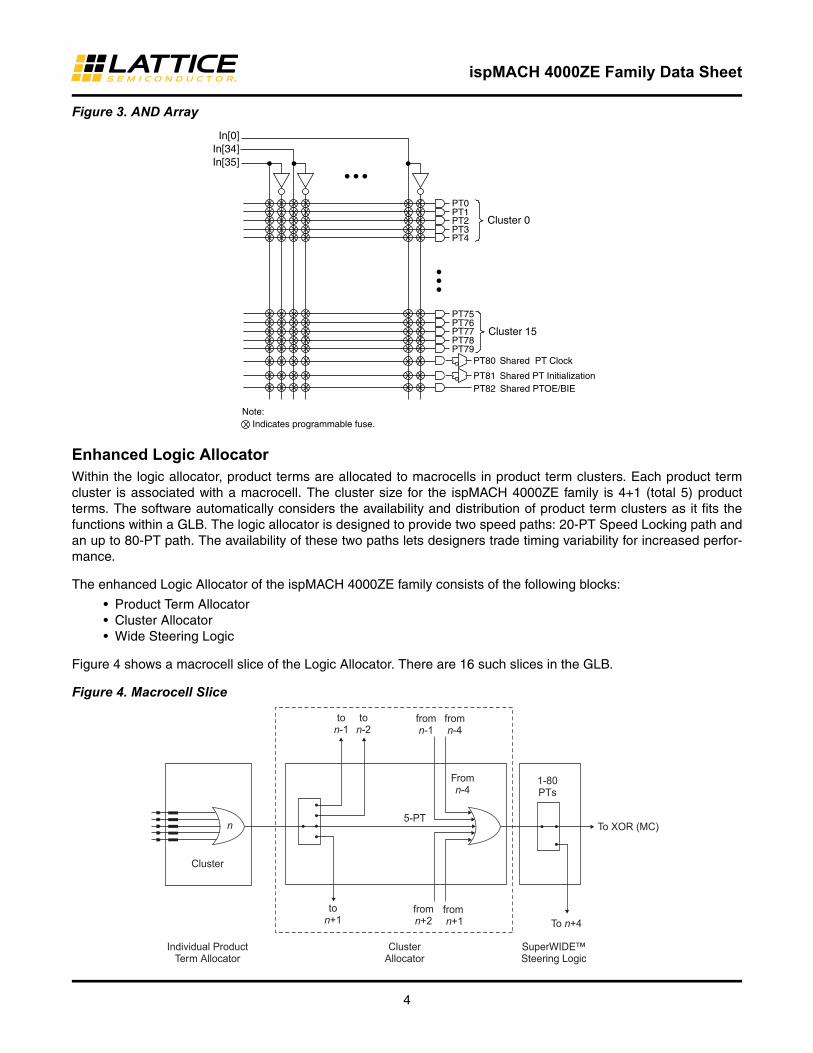
AND ArrayThe programmable AND Array consists of 36 inputs and 83 output product terms. The 36 inputs from the GRP areused to form 72 lines in the AND Array (true and complement of the inputs). Each line in the array can be con-nected to any of the 83 output product terms via a wired-AND. Each of the 80 logic product terms feed the logicallocator with the remaining three control product terms feeding the Shared PT Clock, Shared PT Initialization andShared PT OE. The Shared PT Clock and Shared PT Initialization signals can optionally be inverted before beingfed to the macrocells.
Every set of five product terms from the 80 logic product terms forms a product term cluster starting with PT0.There is one product term cluster for every macrocell in the GLB. Figure 3 is a graphical representation of the ANDArray.
Logi
c A
lloca
tor
36 Inputsfrom GRP 16
Mac
roce
lls
To
OR
P
To GRP
To Product TermOutput Enable Sharing.Also, To Input Enable ofPower Guard on I/Osin the block.
1+OE
16 M
C F
eedb
ack
Sig
nals
ClockGenerator
1+OE
1+OE
1+OE
1+OE
1+OE
1+OE
CLK
0
CLK
1
CLK
2
CLK
3
1+OE
AN
D A
rray
36 In
puts
, 83
Pro
duct
Ter
ms
ispMACH 4000ZE Family Data Sheet
4
Figure 3. AND Array
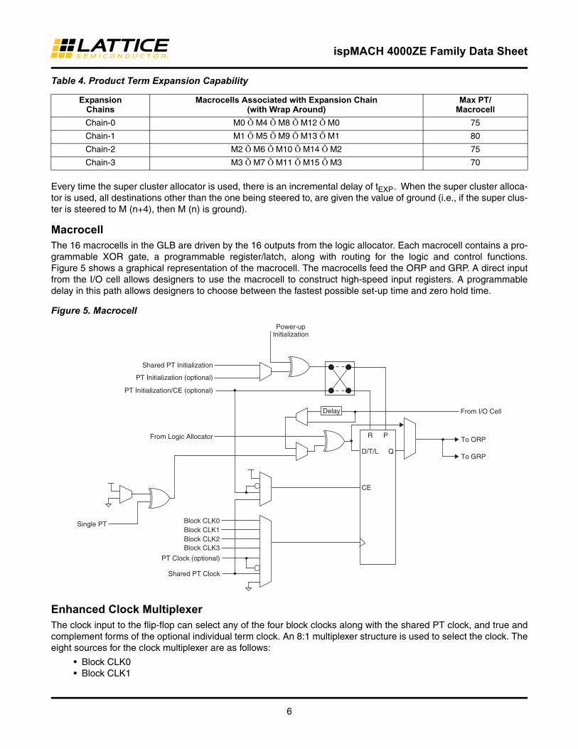
Enhanced Logic AllocatorWithin the logic allocator, product terms are allocated to macrocells in product term clusters. Each product termcluster is associated with a macrocell. The cluster size for the ispMACH 4000ZE family is 4+1 (total 5) productterms. The software automatically considers the availability and distribution of product term clusters as it fits thefunctions within a GLB. The logic allocator is designed to provide two speed paths: 20-PT Speed Locking path andan up to 80-PT path. The availability of these two paths lets designers trade timing variability for increased perfor-mance.
The enhanced Logic Allocator of the ispMACH 4000ZE family consists of the following blocks:
• Product Term Allocator• Cluster Allocator• Wide Steering Logic
Figure 4 shows a macrocell slice of the Logic Allocator. There are 16 such slices in the GLB.
Figure 4. Macrocell Slice
PT0PT1
Cluster 0PT2PT3PT4
In[0]In[34]In[35]
Note: Indicates programmable fuse.
PT80
PT81PT82
Shared PT Clock
Shared PT InitializationShared PTOE/BIE
PT76PT77PT78PT79
PT75
Cluster 15
ton+1
ton-1
ton-2
fromn-1
fromn-4
fromn+2
fromn+1
5-PT
Fromn-4
1-80PTs
To n+4
To XOR (MC)
Cluster
Individual ProductTerm Allocator
ClusterAllocator
SuperWIDE™Steering Logic
n

ispMACH 4000ZE Family Data Sheet
5
Product Term AllocatorThe product term allocator assigns product terms from a cluster to either logic or control applications as requiredby the design being implemented. Product terms that are used as logic are steered into a 5-input OR gate associ-ated with the cluster. Product terms that used for control are steered either to the macrocell or I/O cell associatedwith the cluster. Table 2 shows the available functions for each of the five product terms in the cluster.
Table 2. Individual PT Steering
Cluster AllocatorThe cluster allocator allows clusters to be steered to neighboring macrocells, thus allowing the creation of functions with more product terms. Table 3 shows which clusters can be steered to which macrocells. Used in this manner, the cluster allocator can be used to form functions of up to 20 product terms. Additionally, the cluster allocator accepts inputs from the wide steering logic. Using these inputs, functions up to 80 product terms can be created.
Table 3. Available Clusters for Each Macrocell
Wide Steering LogicThe wide steering logic allows the output of the cluster allocator n to be connected to the input of the cluster alloca-tor n+4. Thus, cluster chains can be formed with up to 80 product terms, supporting wide product term functionsand allowing performance to be increased through a single GLB implementation. Table 4 shows the product termchains.
Product Term Logic Control
PTn Logic PT Single PT for XOR/OR
PTn+1 Logic PT Individual Clock (PT Clock)
PTn+2 Logic PT Individual Initialization or Individual Clock Enable (PT Initialization/CE)
PTn+3 Logic PT Individual Initialization (PT Initialization)
PTn+4 Logic PT Individual OE (PTOE)
Macrocell Available Clusters
M0 — C0 C1 C2
M1 C0 C1 C2 C3
M2 C1 C2 C3 C4
M3 C2 C3 C4 C5
M4 C3 C4 C5 C6
M5 C4 C5 C6 C7
M6 C5 C6 C7 C8
M7 C6 C7 C8 C9
M8 C7 C8 C9 C10
M9 C8 C9 C10 C11
M10 C9 C10 C11 C12
M11 C10 C11 C12 C13
M12 C11 C12 C13 C14
M13 C12 C13 C14 C15
M14 C13 C14 C15 —
M15 C14 C15 — —
ispMACH 4000ZE Family Data Sheet
6
Table 4. Product Term Expansion Capability
Every time the super cluster allocator is used, there is an incremental delay of tEXP. When the super cluster alloca-tor is used, all destinations other than the one being steered to, are given the value of ground (i.e., if the super clus-ter is steered to M (n+4), then M (n) is ground).
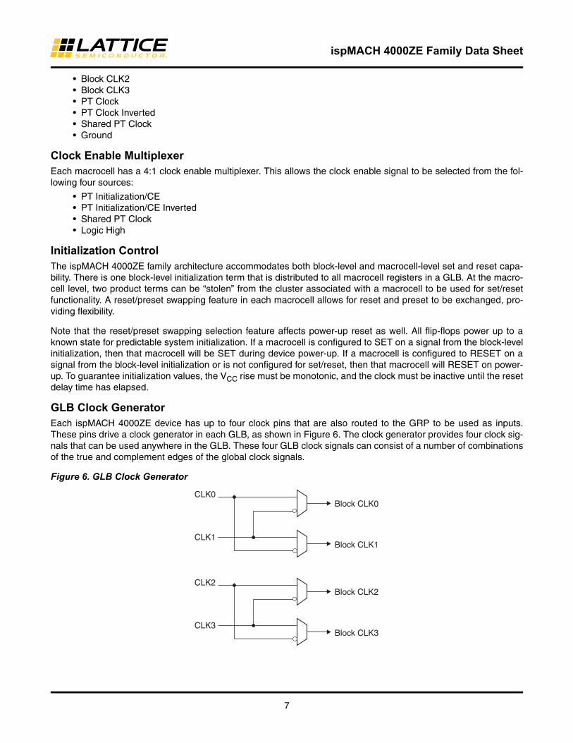
MacrocellThe 16 macrocells in the GLB are driven by the 16 outputs from the logic allocator. Each macrocell contains a pro-grammable XOR gate, a programmable register/latch, along with routing for the logic and control functions.Figure 5 shows a graphical representation of the macrocell. The macrocells feed the ORP and GRP. A direct inputfrom the I/O cell allows designers to use the macrocell to construct high-speed input registers. A programmabledelay in this path allows designers to choose between the fastest possible set-up time and zero hold time.
Figure 5. Macrocell
Enhanced Clock Multiplexer The clock input to the flip-flop can select any of the four block clocks along with the shared PT clock, and true andcomplement forms of the optional individual term clock. An 8:1 multiplexer structure is used to select the clock. Theeight sources for the clock multiplexer are as follows:
• Block CLK0• Block CLK1
ExpansionChains
Macrocells Associated with Expansion Chain(with Wrap Around)
Max PT/Macrocell
Chain-0 M0 Õ M4 Õ M8 Õ M12 Õ M0 75
Chain-1 M1 Õ M5 Õ M9 Õ M13 Õ M1 80
Chain-2 M2 Õ M6 Õ M10 Õ M14 Õ M2 75
Chain-3 M3 Õ M7 Õ M11 Õ M15 Õ M3 70
Single PT Block CLK0Block CLK1Block CLK2Block CLK3
PT Clock (optional)
Shared PT Clock
CE
D/T/L Q
R P
Shared PT Initialization
PT Initialization/CE (optional)
PT Initialization (optional)
From Logic Allocator
Power-upInitialization
To ORP
To GRP
From I/O CellDelay
ispMACH 4000ZE Family Data Sheet
7
• Block CLK2• Block CLK3• PT Clock• PT Clock Inverted• Shared PT Clock• Ground
Clock Enable MultiplexerEach macrocell has a 4:1 clock enable multiplexer. This allows the clock enable signal to be selected from the fol-lowing four sources:
• PT Initialization/CE• PT Initialization/CE Inverted• Shared PT Clock• Logic High
Initialization ControlThe ispMACH 4000ZE family architecture accommodates both block-level and macrocell-level set and reset capa-bility. There is one block-level initialization term that is distributed to all macrocell registers in a GLB. At the macro-cell level, two product terms can be “stolen” from the cluster associated with a macrocell to be used for set/resetfunctionality. A reset/preset swapping feature in each macrocell allows for reset and preset to be exchanged, pro-viding flexibility.
Note that the reset/preset swapping selection feature affects power-up reset as well. All flip-flops power up to aknown state for predictable system initialization. If a macrocell is configured to SET on a signal from the block-levelinitialization, then that macrocell will be SET during device power-up. If a macrocell is configured to RESET on asignal from the block-level initialization or is not configured for set/reset, then that macrocell will RESET on power-up. To guarantee initialization values, the VCC rise must be monotonic, and the clock must be inactive until the resetdelay time has elapsed.
GLB Clock GeneratorEach ispMACH 4000ZE device has up to four clock pins that are also routed to the GRP to be used as inputs.These pins drive a clock generator in each GLB, as shown in Figure 6. The clock generator provides four clock sig-nals that can be used anywhere in the GLB. These four GLB clock signals can consist of a number of combinationsof the true and complement edges of the global clock signals.
Figure 6. GLB Clock Generator
CLK0
CLK1
CLK2
CLK3
Block CLK0
Block CLK1
Block CLK2
Block CLK3
ispMACH 4000ZE Family Data Sheet
8
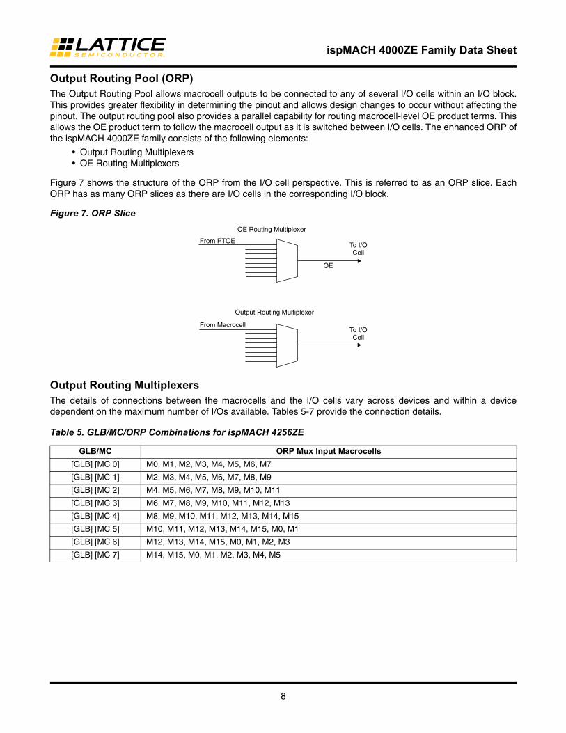
Output Routing Pool (ORP)The Output Routing Pool allows macrocell outputs to be connected to any of several I/O cells within an I/O block.This provides greater flexibility in determining the pinout and allows design changes to occur without affecting thepinout. The output routing pool also provides a parallel capability for routing macrocell-level OE product terms. Thisallows the OE product term to follow the macrocell output as it is switched between I/O cells. The enhanced ORP ofthe ispMACH 4000ZE family consists of the following elements:
• Output Routing Multiplexers• OE Routing Multiplexers
Figure 7 shows the structure of the ORP from the I/O cell perspective. This is referred to as an ORP slice. EachORP has as many ORP slices as there are I/O cells in the corresponding I/O block.
Figure 7. ORP Slice
Output Routing MultiplexersThe details of connections between the macrocells and the I/O cells vary across devices and within a devicedependent on the maximum number of I/Os available. Tables 5-7 provide the connection details.
Table 5. GLB/MC/ORP Combinations for ispMACH 4256ZE
GLB/MC ORP Mux Input Macrocells
[GLB] [MC 0] M0, M1, M2, M3, M4, M5, M6, M7
[GLB] [MC 1] M2, M3, M4, M5, M6, M7, M8, M9
[GLB] [MC 2] M4, M5, M6, M7, M8, M9, M10, M11
[GLB] [MC 3] M6, M7, M8, M9, M10, M11, M12, M13
[GLB] [MC 4] M8, M9, M10, M11, M12, M13, M14, M15
[GLB] [MC 5] M10, M11, M12, M13, M14, M15, M0, M1
[GLB] [MC 6] M12, M13, M14, M15, M0, M1, M2, M3
[GLB] [MC 7] M14, M15, M0, M1, M2, M3, M4, M5
Output Routing Multiplexer
OE Routing Multiplexer
From Macrocell
From PTOETo I/OCell
To I/OCell
OE
ispMACH 4000ZE Family Data Sheet
9
Table 6. GLB/MC/ORP Combinations for ispMACH 4128ZE
Table 7. GLB/MC/ORP Combinations for ispMACH 4032ZE and 4064ZE
Output Enable Routing MultiplexersThe OE Routing Pool provides the corresponding local output enable (OE) product term to the I/O cell.
I/O CellThe I/O cell contains the following programmable elements: output buffer, input buffer, OE multiplexer, Power Guardand bus maintenance circuitry. Figure 8 details the I/O cell.
GLB/MC ORP Mux Input Macrocells
[GLB] [MC 0] M0, M1, M2, M3, M4, M5, M6, M7
[GLB] [MC 1] M1, M2, M3, M4, M5, M6, M7, M8
[GLB] [MC 2] M2, M3, M4, M5, M6, M7, M8, M9
[GLB] [MC 3] M4, M5, M6, M7, M8, M9, M10, M11
[GLB] [MC 4] M5, M6, M7, M8, M9, M10, M11, M12
[GLB] [MC 5] M6, M7, M8, M9, M10, M11, M12, M13
[GLB] [MC 6] M8, M9, M10, M11, M12, M13, M14, M15
[GLB] [MC 7] M9, M10, M11, M12, M13, M14, M15, M0
[GLB] [MC 8] M10, M11, M12, M13, M14, M15, M0, M1
[GLB] [MC 9] M12, M13, M14, M15, M0, M1, M2, M3
[GLB] [MC 10] M13, M14, M15, M0, M1, M2, M3, M4
[GLB] [MC 11] M14, M15, M0, M1, M2, M3, M4, M5
GLB/MC ORP Mux Input Macrocells
[GLB] [MC 0] M0, M1, M2, M3, M4, M5, M6, M7
[GLB] [MC 1] M1, M2, M3, M4, M5, M6, M7, M8
[GLB] [MC 2] M2, M3, M4, M5, M6, M7, M8, M9
[GLB] [MC 3] M3, M4, M5, M6, M7, M8, M9, M10
[GLB] [MC 4] M4, M5, M6, M7, M8, M9, M10, M11
[GLB] [MC 5] M5, M6, M7, M8, M9, M10, M11, M12
[GLB] [MC 6] M6, M7, M8, M9, M10, M11, M12, M13
[GLB] [MC 7] M7, M8, M9, M10, M11, M12, M13, M14
[GLB] [MC 8] M8, M9, M10, M11, M12, M13, M14, M15
[GLB] [MC 9] M9, M10, M11, M12, M13, M14, M15, M0
[GLB] [MC 10] M10, M11, M12, M13, M14, M15, M0, M1
[GLB] [MC 11] M11, M12, M13, M14, M15, M0, M1, M2
[GLB] [MC 12] M12, M13, M14, M15, M0, M1, M2, M3
[GLB] [MC 13] M13, M14, M15, M0, M1, M2, M3, M4
[GLB] [MC 14] M14, M15, M0, M1, M2, M3, M4, M5
[GLB] [MC 15] M15, M0, M1, M2, M3, M4, M5, M6

ispMACH 4000ZE Family Data Sheet
10
Figure 8. I/O Cell
Each output supports a variety of output standards dependent on the VCCO supplied to its I/O bank. Outputs canalso be configured for open drain operation. Each input can be programmed to support a variety of standards, inde-pendent of the VCCO supplied to its I/O bank. The I/O standards supported are:
• LVTTL • LVCMOS 1.8• LVCMOS 3.3 • LVCMOS 1.5• LVCMOS 2.5 • 3.3V PCI Compatible
All of the I/Os and dedicated inputs have the capability to provide a bus-keeper latch, pull-up resistor or pull-downresistor selectable on a “per-pin” basis. A fourth option is to provide none of these. The default in both hardwareand software is such that when the device is erased or if the user does not specify, the input structure is configuredto be a Pull-down Resistor.
Each ispMACH 4000ZE device I/O has an individually programmable output slew rate control bit. Each output canbe individually configured for fast slew or slow slew. The typical edge rate difference between fast and slow slewsetting is 20%. For high-speed designs with long, unterminated traces, the slow-slew rate will introduce fewerreflections, less noise and keep ground bounce to a minimum. For designs with short traces or well terminatedlines, the fast slew rate can be used to achieve the highest speed.
The ispMACH 4000ZE family has an always on, 200mV typical hysteresis for each input operational at 3.3V and2.5V. This provides improved noise immunity for slow transitioning signals.
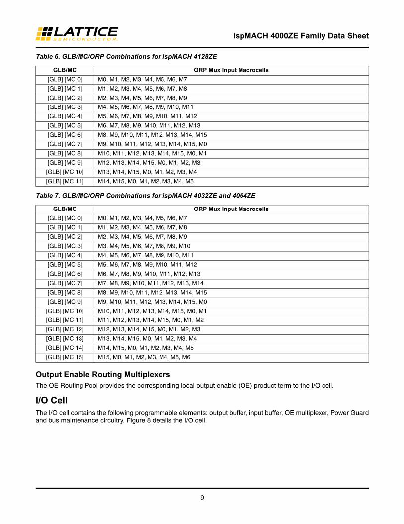
Power GuardPower Guard allows easier achievement of standby current in the system. As shown in Figure 9, this feature con-sists of an enabling multiplexer between an I/O pin and input buffer, and its associated circuitry inside the device.
If the enable signal (E) is held low, all inputs (D) can be optionally isolated (guarded), such that, if any of these weretoggled, it would not cause any toggle on internal pins (Q), thus, a toggling I/O pin will not cause any internaldynamic power consumption.
To Macrocell
To GRP
VCCO
GOE 0
GOE 1
GOE 2
GOE 3
VCC
From ORP
From ORP
0
1
Block Input Enable (BIE)(From Block PT)
Power Guard Disable Fuse (PGDF)
0
1
Power Guard
I/O Bus Maintenance
VCCO
ispMACH 4000ZE Family Data Sheet
11
Figure 9. Power Guard
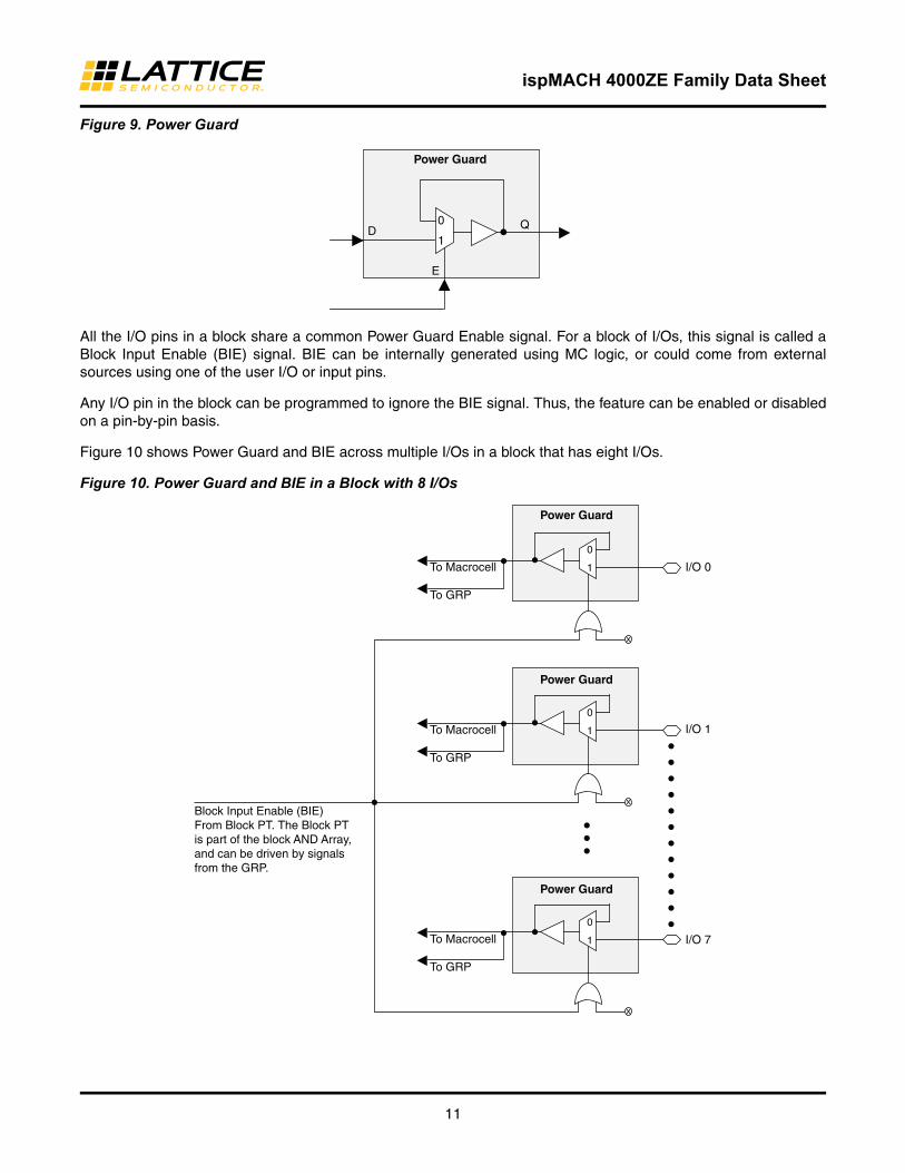
All the I/O pins in a block share a common Power Guard Enable signal. For a block of I/Os, this signal is called aBlock Input Enable (BIE) signal. BIE can be internally generated using MC logic, or could come from externalsources using one of the user I/O or input pins.
Any I/O pin in the block can be programmed to ignore the BIE signal. Thus, the feature can be enabled or disabledon a pin-by-pin basis.
Figure 10 shows Power Guard and BIE across multiple I/Os in a block that has eight I/Os.
Figure 10. Power Guard and BIE in a Block with 8 I/Os
0 1
E
Q D
Power Guard
Power Guard
To Macrocell I/O 0
I/O 1
I/O 7
To GRP
0
1
To Macrocell
To GRP
To Macrocell
To GRP
Block Input Enable (BIE)From Block PT. The Block PT is part of the block AND Array, and can be driven by signals from the GRP.
Power Guard
Power Guard
0
1
0
1
ispMACH 4000ZE Family Data Sheet
12
The number of BIE inputs, thus the number of Power Guard “Blocks” that can exist in a device, depends on thedevice size. Table 8 shows the number of BIE signals available in the ispMACH 4000ZE family. The number of I/Osavailable in each block is shown in the Ordering Information section of this data sheet.
Table 8. Number of BIE Signals Available in ispMACH 4000ZE Devices
Power Guard for Dedicated InputsPower Guard can optionally be applied to the dedicated inputs. The dedicated inputs and clocks are controlled bythe BIE of the logic blocks shown in Tables 9 and 10.
Table 10. Dedicated Inputs to BIE Association
For more information on the Power Guard function refer to TN1174, Advanced Features of the ispMACH 4000ZEFamily.
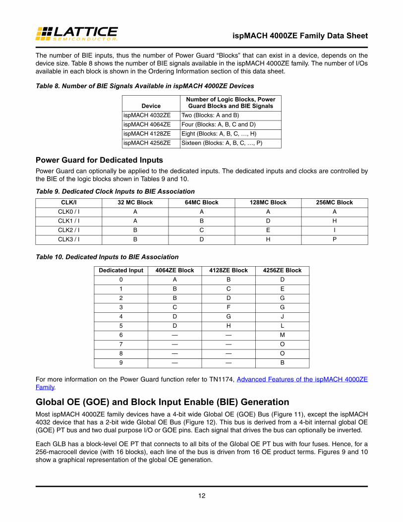
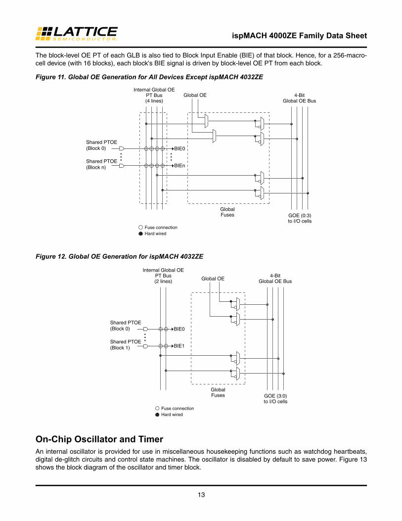
Global OE (GOE) and Block Input Enable (BIE) GenerationMost ispMACH 4000ZE family devices have a 4-bit wide Global OE (GOE) Bus (Figure 11), except the ispMACH4032 device that has a 2-bit wide Global OE Bus (Figure 12). This bus is derived from a 4-bit internal global OE(GOE) PT bus and two dual purpose I/O or GOE pins. Each signal that drives the bus can optionally be inverted.
Each GLB has a block-level OE PT that connects to all bits of the Global OE PT bus with four fuses. Hence, for a256-macrocell device (with 16 blocks), each line of the bus is driven from 16 OE product terms. Figures 9 and 10show a graphical representation of the global OE generation.
DeviceNumber of Logic Blocks, Power Guard Blocks and BIE Signals
ispMACH 4032ZE Two (Blocks: A and B)
ispMACH 4064ZE Four (Blocks: A, B, C and D)
ispMACH 4128ZE Eight (Blocks: A, B, C, …, H)
ispMACH 4256ZE Sixteen (Blocks: A, B, C, …, P)
Table 9. Dedicated Clock Inputs to BIE Association
CLK/I 32 MC Block 64MC Block 128MC Block 256MC Block
CLK0 / I A A A A
CLK1 / I A B D H
CLK2 / I B C E I
CLK3 / I B D H P
Dedicated Input 4064ZE Block 4128ZE Block 4256ZE Block
0 A B D
1 B C E
2 B D G
3 C F G
4 D G J
5 D H L
6 — — M
7 — — O
8 — — O
9 — — B
ispMACH 4000ZE Family Data Sheet
13
The block-level OE PT of each GLB is also tied to Block Input Enable (BIE) of that block. Hence, for a 256-macro-cell device (with 16 blocks), each block's BIE signal is driven by block-level OE PT from each block.
Figure 11. Global OE Generation for All Devices Except ispMACH 4032ZE
Figure 12. Global OE Generation for ispMACH 4032ZE
On-Chip Oscillator and TimerAn internal oscillator is provided for use in miscellaneous housekeeping functions such as watchdog heartbeats,digital de-glitch circuits and control state machines. The oscillator is disabled by default to save power. Figure 13shows the block diagram of the oscillator and timer block.
Shared PTOE(Block 0)
Shared PTOE(Block n)
BIE0
BIEn
GlobalFuses GOE (0:3)
to I/O cells
Internal Global OEPT Bus(4 lines)
4-BitGlobal OE Bus
Global OE
Fuse connectionHard wired
Shared PTOE(Block 0)
Shared PTOE(Block 1)
GlobalFuses GOE (3:0)
to I/O cells
Internal Global OEPT Bus(2 lines)
4-BitGlobal OE BusGlobal OE
Fuse connectionHard wired
BIE0
BIE1
ispMACH 4000ZE Family Data Sheet
14
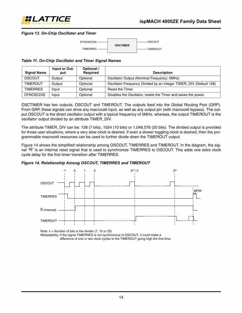
Figure 13. On-Chip Oscillator and Timer
Table 11. On-Chip Oscillator and Timer Signal Names
OSCTIMER has two outputs, OSCOUT and TIMEROUT. The outputs feed into the Global Routing Pool (GRP).From GRP, these signals can drive any macrocell input, as well as any output pin (with macrocell bypass). The out-put OSCOUT is the direct oscillator output with a typical frequency of 5MHz, whereas, the output TIMEROUT is theoscillator output divided by an attribute TIMER_DIV.
The attribute TIMER_DIV can be: 128 (7 bits), 1024 (10 bits) or 1,048,576 (20 bits). The divided output is providedfor those user situations, where a very slow clock is desired. If even a slower toggling clock is desired, then the pro-grammable macrocell resources can be used to further divide down the TIMEROUT output.
Figure 14 shows the simplified relationship among OSCOUT, TIMERRES and TIMEROUT. In the diagram, the sig-nal “R” is an internal reset signal that is used to synchronize TIMERRES to OSCOUT. This adds one extra clockcycle delay for the first timer transition after TIMERRES.
Figure 14. Relationship Among OSCOUT, TIMERRES and TIMEROUT
Signal NameInput or Out-
putOptional / Required Description
OSCOUT Output Optional Oscillator Output (Nominal Frequency: 5MHz)
TIMEROUT Output Optional Oscillator Frequency Divided by an integer TIMER_DIV (Default 128)
TIMERRES Input Optional Reset the Timer
DYNOSCDIS Input Optional Disables the Oscillator, resets the Timer and saves the power.
OSCTIMEROSCOUT
TIMEROUTTIMERRES
DYNOSCDIS
Note: n = Number of bits in the divider (7, 10 or 20)Metastability: If the signal TIMERRES is not synchronous to OSCOUT, it could make a difference of one or two clock cycles to the TIMEROUT going high the first time.
OSCOUT
2 2n / 2 2n10-1
TIMERRES
TIMEROUT
R (Internal)
MPW

ispMACH 4000ZE Family Data Sheet
15
Some Simple Use ScenariosThe following diagrams show a few simple examples that omit optional signals for the OSCTIMER block:
A. An oscillator giving 5MHz nominal clock
B. An oscillator that can be disabled with an external signal (5MHz nominal clock)
C. An oscillator giving approximately 5 Hz nominal clock (TIMER_DIV = 220 (1,048,576))
D. An oscillator giving two output clocks: ~5MHz and ~5KHz (TIMER_DIV= 210 (1,024))
OSCTIMER Integration With CPLD FabricThe OSCTIMER is integrated into the CPLD fabric using the Global Routing Pool (GRP). The macrocell (MC) feed-back path for two macrocells is augmented with a programmable multiplexer, as shown in Figure 15. The OSC-TIMER outputs (OSCOUT and TIMEROUT) can optionally drive the GRP lines, whereas the macrocell outputs candrive the optional OSCTIMER inputs TIMERRES and DYNOSCDIS.
Figure 15. OSCTIMER Integration With CPLD Fabric
Table 12 shows how these two MCs are designated in each of the ispMACH4000ZE device.
OSCTIME R TI ME R_DIV= N/A OSCOUT
(A) A simple 5MHz oscillator. (B) An oscillator with dynamic disable.
(D) Oscillator with two outputs (5MHz and 5KHz).(C) A simple 5Hz oscillator.
DYNOS CD IS OSCTIME R TI ME R_DIV= N/A OSCOUT
OSCTIME R TI ME R_DIV= 220 TIMEROUT
OSCTIME R TI ME R_DIV= 210
OSCOUT
TIMEROUT
1
0
1
0
1
0
1
0
A Regular Macrocell
OSC Macrocell
TIMER Macrocell
To GRP
To GRP
To GRP
MacrocellFeedbackSignal
Macrocell 15FeedbackSignal
OSCOUT DYNOSCDIS
TIMEROUT TIMERRES
Macrocell 15FeedbackSignal

ispMACH 4000ZE Family Data Sheet
16
Table 12. OSC and TIMER MC Designation
Zero Power/Low Power and Power ManagementThe ispMACH 4000ZE family is designed with high speed low power design techniques to offer both high speedand low power. With an advanced E2 low power cell and non sense-amplifier design approach (full CMOS logicapproach), the ispMACH 4000ZE family offers fast pin-to-pin speeds, while simultaneously delivering low standbypower without needing any “turbo bits” or other power management schemes associated with a traditional sense-amplifier approach.
The zero power ispMACH 4000ZE is based on the 1.8V ispMACH 4000Z family. With innovative circuit designchanges, the ispMACH 4000ZE family is able to achieve the industry’s lowest static power.
IEEE 1149.1-Compliant Boundary Scan TestabilityAll ispMACH 4000ZE devices have boundary scan cells and are compliant to the IEEE 1149.1 standard. Thisallows functional testing of the circuit board on which the device is mounted through a serial scan path that canaccess all critical logic notes. Internal registers are linked internally, allowing test data to be shifted in and loadeddirectly onto test nodes, or test node data to be captured and shifted out for verification. In addition, these devicescan be linked into a board-level serial scan path for more board-level testing. The test access port operates with anLVCMOS interface that corresponds to the power supply voltage.
I/O Quick ConfigurationTo facilitate the most efficient board test, the physical nature of the I/O cells must be set before running any continu-ity tests. As these tests are fast, by nature, the overhead and time that is required for configuration of the I/Os’physical nature should be minimal so that board test time is minimized. The ispMACH 4000ZE family of devicesallows this by offering the user the ability to quickly configure the physical nature of the I/O cells. This quick config-uration takes milliseconds to complete, whereas it takes seconds for the entire device to be programmed. Lattice'sispVM™ System programming software can either perform the quick configuration through the PC parallel port, orcan generate the ATE or test vectors necessary for a third-party test system.
IEEE 1532-Compliant In-System ProgrammingProgramming devices in-system provides a number of significant benefits including: rapid prototyping, lower inven-tory levels, higher quality and the ability to make in-field modifications. All ispMACH 4000ZE devices provide In-System Programming (ISP™) capability through the Boundary Scan Test Access Port. This capability has beenimplemented in a manner that ensures that the port remains complaint to the IEEE 1149.1 standard. By using IEEE1149.1 as the communication interface through which ISP is achieved, users get the benefit of a standard, well-defined interface. All ispMACH 4000ZE devices are also compliant with the IEEE 1532 standard.
The ispMACH 4000ZE devices can be programmed across the commercial temperature and voltage range. ThePC-based Lattice software facilitates in-system programming of ispMACH 4000ZE devices. The software takes theJEDEC file output produced by the design implementation software, along with information about the scan chain,and creates a set of vectors used to drive the scan chain. The software can use these vectors to drive a scan chainvia the parallel port of a PC. Alternatively, the software can output files in formats understood by common auto-
Device Macrocell Block Number MC Number
ispMACH 4032ZE OSC MCTIMER MC
AB
1515
ispMACH 4064ZE OSC MCTIMER MC
AD
1515
ispMACH 4128ZE OSC MCTIMER MC
AG
1515
ispMACH 4256ZE OSC MCTIMER MC
CF
1515
ispMACH 4000ZE Family Data Sheet
17
mated test equipment. This equipment can then be used to program ispMACH 4000ZE devices during the testingof a circuit board.
User Electronic SignatureThe User Electronic Signature (UES) allows the designer to include identification bits or serial numbers inside thedevice, stored in E2CMOS memory. The ispMACH 4000ZE device contains 32 UES bits that can be configured bythe user to store unique data such as ID codes, revision numbers or inventory control codes.
Security BitA programmable security bit is provided on the ispMACH 4000ZE devices as a deterrent to unauthorized copying ofthe array configuration patterns. Once programmed, this bit defeats readback of the programmed pattern by adevice programmer, securing proprietary designs from competitors. Programming and verification are alsodefeated by the security bit. The bit can only be reset by erasing the entire device.
Hot SocketingThe ispMACH 4000ZE devices are well-suited for applications that require hot socketing capability. Hot socketing adevice requires that the device, during power-up and down, can tolerate active signals on the I/Os and inputs with-out being damaged. Additionally, it requires that the effects of I/O pin loading be minimal on active signals. The isp-MACH 4000ZE devices provide this capability for input voltages in the range 0V to 3.0V.
Density MigrationThe ispMACH 4000ZE family has been designed to ensure that different density devices in the same package havethe same pin-out. Furthermore, the architecture ensures a high success rate when performing design migrationfrom lower density parts to higher density parts. In many cases, it is possible to shift a lower utilization design tar-geted for a high density device to a lower density device. However, the exact details of the final resource utilizationwill impact the likely success in each case.
ispMACH 4000ZE Family Data Sheet
18
Absolute Maximum Ratings1, 2, 3, 4
Supply Voltage (VCC) . . . . . . . . . . . . . . . . . . . . . . -0.5 to 2.5V
Output Supply Voltage (VCCO) . . . . . . . . . . . . . . . -0.5 to 4.5V
Input or I/O Tristate Voltage Applied5, 6 . . . . . . . . . -0.5 to 5.5V
Storage Temperature . . . . . . . . . . . . . . . . . . . . . . -65 to 150°C
Junction Temperature (Tj) with Power Applied . . . -55 to 150°C
1. Stress above those listed under the “Absolute Maximum Ratings” may cause permanent damage to the device. Functionaloperation of the device at these or any other conditions above those indicated in the operational sections of this specificationis not implied.
2. Compliance with Lattice Thermal Management document is required.
3. All voltages referenced to GND.
4. Please refer to the Lattice ispMACH 4000V/B/C/ZC/ZE Product Family Qualification Summary for complete data, includingthe ESD performance data.
5. Undershoot of -2V and overshoot of (VIH (MAX) + 2V), up to a total pin voltage of 6V is permitted for a duration of <20ns.
6. Maximum of 64 I/Os per device with VIN > 3.6V is allowed.
Recommended Operating Conditions
Erase Reprogram Specifications
Hot Socketing Characteristics1,2,3
Symbol Parameter Min. Max. Units
VCC Supply VoltageStandard Voltage Operation 1.7 1.9 V
Extended Voltage Operation 1.61 1.9 V
TjJunction Temperature (Commercial) 0 90 °C
Junction Temperature (Industrial) -40 105 °C
1. Devices operating at 1.6V can expect performance degradation up to 35%.
Parameter Min. Max. Units
Erase/Reprogram Cycle 1,000 — Cycles
Note: Valid over commercial temperature range.
Symbol Parameter Condition Min. Typ. Max. Units
IDK Input or I/O Leakage Current0 VIN 3.0V, Tj = 105°C — ±30 ±150 µA
0 VIN 3.0V, Tj = 130°C — ±30 ±200 µA
1. Insensitive to sequence of VCC or VCCO. However, assumes monotonic rise/fall rates for VCC and VCCO, provided (VIN - VCCO) 3.6V.2. 0 < VCC < VCC (MAX), 0 < VCCO < VCCO (MAX). 3. IDK is additive to IPU, IPD or IBH. Device defaults to pull-up until fuse circuitry is active.
ispMACH 4000ZE Family Data Sheet
19
I/O Recommended Operating Conditions
DC Electrical CharacteristicsOver Recommended Operating Conditions
Standard
VCCO (V)1
Min. Max.
LVTTL 3.0 3.6
LVCMOS 3.3 3.0 3.6
Extended LVCMOS 3.3 2.7 3.6
LVCMOS 2.5 2.3 2.7
LVCMOS 1.8 1.65 1.95
LVCMOS 1.5 1.4 1.6
PCI 3.3 3.0 3.6
1. Typical values for VCCO are the average of the min. and max. values.
Symbol Parameter Condition Min. Typ. Max. Units
IIL, IIH1, 2 Input Leakage Current 0 VIN < VCCO — 0.5 1 µA
IIH1 Input High Leakage Current VCCO < VIN 5.5V — — 10 µA
IPU I/O Weak Pull-up Resistor Current 0 VIN 0.7VCCO -20 — -150 µA
IPD I/O Weak Pull-down Resistor Current VIL (MAX) VIN VIH (MAX) 30 — 150 µA
IBHLS Bus Hold Low Sustaining Current VIN = VIL (MAX) 30 — — µA
IBHHS Bus Hold High Sustaining Current VIN = 0.7 VCCO -20 — — µA
IBHLO Bus Hold Low Overdrive Current 0V VIN VBHT — — 150 µA
IBHHO Bus Hold High Overdrive Current VBHT VIN VCCO — — -150 µA
VBHT Bus Hold Trip Points — VCCO * 0.35 — VCCO * 0.65 V
C1 I/O Capacitance3VCCO = 3.3V, 2.5V, 1.8V, 1.5V —
8—
pfVCC = 1.8V, VIO = 0 to VIH (MAX) — —
C2 Clock Capacitance3VCCO = 3.3V, 2.5V, 1.8V, 1.5V —
6—
pfVCC = 1.8V, VIO = 0 to VIH (MAX) — —
C3 Global Input Capacitance3VCCO = 3.3V, 2.5V, 1.8V, 1.5V —
6—
pfVCC = 1.8V, VIO = 0 to VIH (MAX) — —
1. Input or I/O leakage current is measured with the pin configured as an input or as an I/O with the output driver tristated. It is not measured with the output driver active. Bus maintenance circuits are disabled.
2. IIH excursions of up to 1.5µA maximum per pin above the spec limit may be observed for certain voltage conditions on no more than 10% of the device’s I/O pins.
3. Measured TA = 25°C, f = 1.0MHz.
ispMACH 4000ZE Family Data Sheet
20
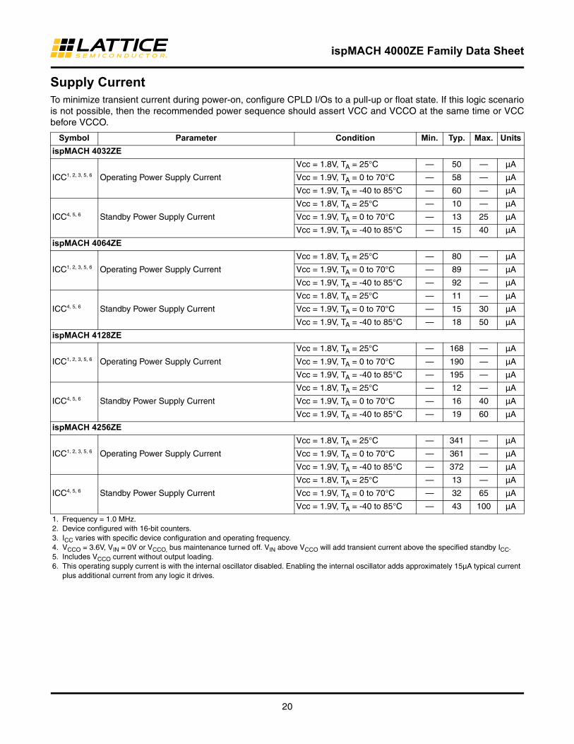
Supply CurrentTo minimize transient current during power-on, configure CPLD I/Os to a pull-up or float state. If this logic scenariois not possible, then the recommended power sequence should assert VCC and VCCO at the same time or VCCbefore VCCO.
Symbol Parameter Condition Min. Typ. Max. Units
ispMACH 4032ZE
ICC1, 2, 3, 5, 6 Operating Power Supply Current
Vcc = 1.8V, TA = 25°C — 50 — µA
Vcc = 1.9V, TA = 0 to 70°C — 58 — µA
Vcc = 1.9V, TA = -40 to 85°C — 60 — µA
ICC4, 5, 6 Standby Power Supply Current
Vcc = 1.8V, TA = 25°C — 10 — µA
Vcc = 1.9V, TA = 0 to 70°C — 13 25 µA
Vcc = 1.9V, TA = -40 to 85°C — 15 40 µA
ispMACH 4064ZE
ICC1, 2, 3, 5, 6 Operating Power Supply Current
Vcc = 1.8V, TA = 25°C — 80 — µA
Vcc = 1.9V, TA = 0 to 70°C — 89 — µA
Vcc = 1.9V, TA = -40 to 85°C — 92 — µA
ICC4, 5, 6 Standby Power Supply Current
Vcc = 1.8V, TA = 25°C — 11 — µA
Vcc = 1.9V, TA = 0 to 70°C — 15 30 µA
Vcc = 1.9V, TA = -40 to 85°C — 18 50 µA
ispMACH 4128ZE
ICC1, 2, 3, 5, 6 Operating Power Supply Current
Vcc = 1.8V, TA = 25°C — 168 — µA
Vcc = 1.9V, TA = 0 to 70°C — 190 — µA
Vcc = 1.9V, TA = -40 to 85°C — 195 — µA
ICC4, 5, 6 Standby Power Supply Current
Vcc = 1.8V, TA = 25°C — 12 — µA
Vcc = 1.9V, TA = 0 to 70°C — 16 40 µA
Vcc = 1.9V, TA = -40 to 85°C — 19 60 µA
ispMACH 4256ZE
ICC1, 2, 3, 5, 6 Operating Power Supply Current
Vcc = 1.8V, TA = 25°C — 341 — µA
Vcc = 1.9V, TA = 0 to 70°C — 361 — µA
Vcc = 1.9V, TA = -40 to 85°C — 372 — µA
ICC4, 5, 6 Standby Power Supply Current
Vcc = 1.8V, TA = 25°C — 13 — µA
Vcc = 1.9V, TA = 0 to 70°C — 32 65 µA
Vcc = 1.9V, TA = -40 to 85°C — 43 100 µA
1. Frequency = 1.0 MHz. 2. Device configured with 16-bit counters. 3. ICC varies with specific device configuration and operating frequency. 4. VCCO = 3.6V, VIN = 0V or VCCO, bus maintenance turned off. VIN above VCCO will add transient current above the specified standby ICC.5. Includes VCCO current without output loading.6. This operating supply current is with the internal oscillator disabled. Enabling the internal oscillator adds approximately 15µA typical current
plus additional current from any logic it drives.
ispMACH 4000ZE Family Data Sheet
21
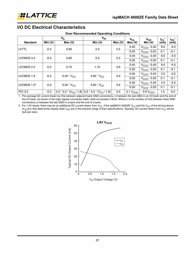
I/O DC Electrical CharacteristicsOver Recommended Operating Conditions
Standard
VIL VIH VOLMax (V)
VOHMin (V)
IOL1
(mA)IOH
1
(mA)Min (V) Max (V) Min (V) Max (V)
LVTTL -0.3 0.80 2.0 5.50.40 VCCO - 0.40 8.0 -4.0
0.20 VCCO - 0.20 0.1 -0.1
LVCMOS 3.3 -0.3 0.80 2.0 5.50.40 VCCO - 0.40 8.0 -4.0
0.20 VCCO - 0.20 0.1 -0.1
LVCMOS 2.5 -0.3 0.70 1.70 3.60.40 VCCO - 0.40 8.0 -4.0
0.20 VCCO - 0.20 0.1 -0.1
LVCMOS 1.8 -0.3 0.35 * VCC 0.65 * VCC 3.60.40 VCCO - 0.45 2.0 -2.0
0.20 VCCO - 0.20 0.1 -0.1
LVCMOS 1.52 -0.3 0.35 * VCC 0.65 * VCC 3.60.40 VCCO - 0.45 2.0 -2.0
0.20 VCCO - 0.20 0.1 -0.1
PCI 3.3 -0.3 0.3 * 3.3 * (VCC / 1.8) 0.5 * 3.3 * (VCC / 1.8) 5.5 0.1 VCCO 0.9 VCCO 1.5 -0.5
1. The average DC current drawn by I/Os between adjacent bank GND connections, or between the last GND in an I/O bank and the end of the I/O bank, as shown in the logic signals connection table, shall not exceed n*8mA. Where n is the number of I/Os between bank GND connections or between the last GND in a bank and the end of a bank.
2. For 1.5V inputs, there may be an additional DC current drawn from VCC, if the ispMACH 4000ZE VCC and the VCC of the driving device (VCCd-d; that determines steady state VIH) are in the extreme range of their specifications. Typically, DC current drawn from VCC will be 2µA per input.
VO Output Voltage (V)
00
10
20
30
40
50
60
2.01.51.00.5
Typ
ical
I/O
Out
put C
urre
nt (
mA
)
1.8V VCCO
IOH
IOL
ispMACH 4000ZE Family Data Sheet
22
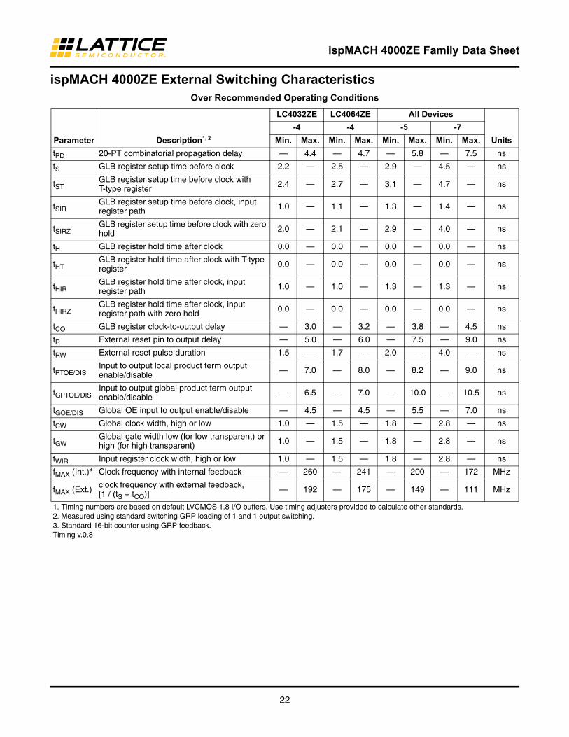
ispMACH 4000ZE External Switching CharacteristicsOver Recommended Operating Conditions
Parameter Description1, 2
LC4032ZE LC4064ZE All Devices
Units
-4 -4 -5 -7
Min. Max. Min. Max. Min. Max. Min. Max.
tPD 20-PT combinatorial propagation delay — 4.4 — 4.7 — 5.8 — 7.5 ns
tS GLB register setup time before clock 2.2 — 2.5 — 2.9 — 4.5 — ns
tSTGLB register setup time before clock with T-type register 2.4 — 2.7 — 3.1 — 4.7 — ns
tSIRGLB register setup time before clock, input register path 1.0 — 1.1 — 1.3 — 1.4 — ns
tSIRZGLB register setup time before clock with zero hold 2.0 — 2.1 — 2.9 — 4.0 — ns
tH GLB register hold time after clock 0.0 — 0.0 — 0.0 — 0.0 — ns
tHTGLB register hold time after clock with T-type register 0.0 — 0.0 — 0.0 — 0.0 — ns
tHIRGLB register hold time after clock, input register path 1.0 — 1.0 — 1.3 — 1.3 — ns
tHIRZGLB register hold time after clock, inputregister path with zero hold 0.0 — 0.0 — 0.0 — 0.0 — ns
tCO GLB register clock-to-output delay — 3.0 — 3.2 — 3.8 — 4.5 ns
tR External reset pin to output delay — 5.0 — 6.0 — 7.5 — 9.0 ns
tRW External reset pulse duration 1.5 — 1.7 — 2.0 — 4.0 — ns
tPTOE/DISInput to output local product term output enable/disable — 7.0 — 8.0 — 8.2 — 9.0 ns
tGPTOE/DISInput to output global product term output enable/disable — 6.5 — 7.0 — 10.0 — 10.5 ns
tGOE/DIS Global OE input to output enable/disable — 4.5 — 4.5 — 5.5 — 7.0 ns
tCW Global clock width, high or low 1.0 — 1.5 — 1.8 — 2.8 — ns
tGWGlobal gate width low (for low transparent) or high (for high transparent) 1.0 — 1.5 — 1.8 — 2.8 — ns
tWIR Input register clock width, high or low 1.0 — 1.5 — 1.8 — 2.8 — ns
fMAX (Int.)3 Clock frequency with internal feedback — 260 — 241 — 200 — 172 MHz
fMAX (Ext.) clock frequency with external feedback, [1 / (tS + tCO)] — 192 — 175 — 149 — 111 MHz
1. Timing numbers are based on default LVCMOS 1.8 I/O buffers. Use timing adjusters provided to calculate other standards.2. Measured using standard switching GRP loading of 1 and 1 output switching.3. Standard 16-bit counter using GRP feedback.Timing v.0.8
ispMACH 4000ZE Family Data Sheet
23
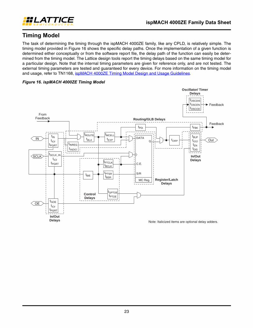
Timing ModelThe task of determining the timing through the ispMACH 4000ZE family, like any CPLD, is relatively simple. Thetiming model provided in Figure 16 shows the specific delay paths. Once the implementation of a given function isdetermined either conceptually or from the software report file, the delay path of the function can easily be deter-mined from the timing model. The Lattice design tools report the timing delays based on the same timing model fora particular design. Note that the internal timing parameters are given for reference only, and are not tested. Theexternal timing parameters are tested and guaranteed for every device. For more information on the timing modeland usage, refer to TN1168, ispMACH 4000ZE Timing Model Design and Usage Guidelines.
Figure 16. ispMACH 4000ZE Timing Model
DATA
MC Reg.
C.E.
S/R
Q
SCLK
IN
OE
In/OutDelays
Oscillator/ TimerDelays
In/OutDelays
ControlDelays
Register/LatchDelays
Routing/GLB Delays
Out
Note: Italicized items are optional delay adders.
tFBK
Feedback
Feedback
FromFeedback
tBUFtMCELL
tPTCLKtBCLK
tPTSRtBIE tBSR
tGPTOEtPTOE
tEXP
tROUTE
tOSCDIStOSCENtOSCOD
tBLA
tINREG
tINDIO
tIN
tPGRT
tIOI
tGCLK_IN
tIOItPGRT
tPGRT
tGOE
tIOI
tPDi
tIOOtORP
tENtDIS
ispMACH 4000ZE Family Data Sheet
24
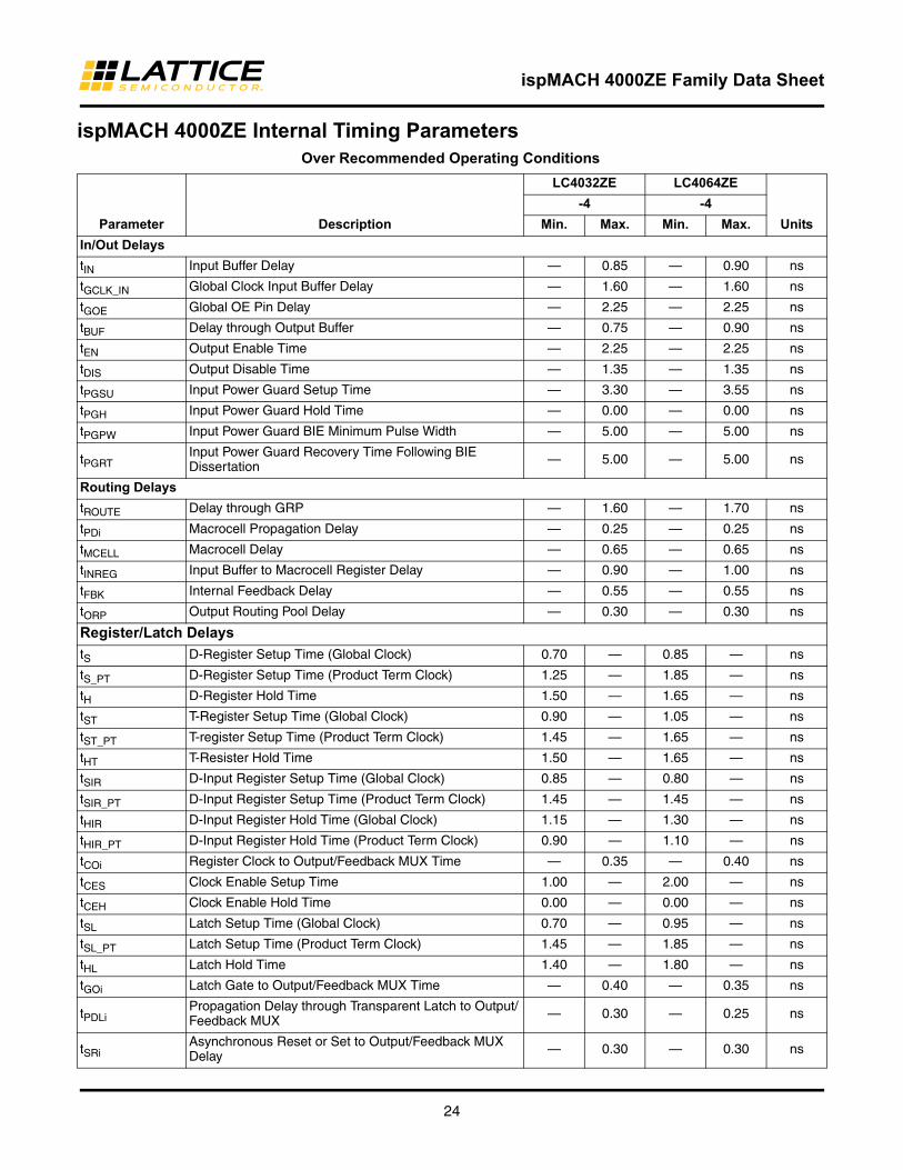
ispMACH 4000ZE Internal Timing ParametersOver Recommended Operating Conditions
Parameter Description
LC4032ZE LC4064ZE
Units
-4 -4
Min. Max. Min. Max.
In/Out Delays
tIN Input Buffer Delay — 0.85 — 0.90 ns
tGCLK_IN Global Clock Input Buffer Delay — 1.60 — 1.60 ns
tGOE Global OE Pin Delay — 2.25 — 2.25 ns
tBUF Delay through Output Buffer — 0.75 — 0.90 ns
tEN Output Enable Time — 2.25 — 2.25 ns
tDIS Output Disable Time — 1.35 — 1.35 ns
tPGSU Input Power Guard Setup Time — 3.30 — 3.55 ns
tPGH Input Power Guard Hold Time — 0.00 — 0.00 ns
tPGPW Input Power Guard BIE Minimum Pulse Width — 5.00 — 5.00 ns
tPGRTInput Power Guard Recovery Time Following BIE Dissertation — 5.00 — 5.00 ns
Routing Delays
tROUTE Delay through GRP — 1.60 — 1.70 ns
tPDi Macrocell Propagation Delay — 0.25 — 0.25 ns
tMCELL Macrocell Delay — 0.65 — 0.65 ns
tINREG Input Buffer to Macrocell Register Delay — 0.90 — 1.00 ns
tFBK Internal Feedback Delay — 0.55 — 0.55 ns
tORP Output Routing Pool Delay — 0.30 — 0.30 ns
Register/Latch Delays
tS D-Register Setup Time (Global Clock) 0.70 — 0.85 — ns
tS_PT D-Register Setup Time (Product Term Clock) 1.25 — 1.85 — ns
tH D-Register Hold Time 1.50 — 1.65 — ns
tST T-Register Setup Time (Global Clock) 0.90 — 1.05 — ns
tST_PT T-register Setup Time (Product Term Clock) 1.45 — 1.65 — ns
tHT T-Resister Hold Time 1.50 — 1.65 — ns
tSIR D-Input Register Setup Time (Global Clock) 0.85 — 0.80 — ns
tSIR_PT D-Input Register Setup Time (Product Term Clock) 1.45 — 1.45 — ns
tHIR D-Input Register Hold Time (Global Clock) 1.15 — 1.30 — ns
tHIR_PT D-Input Register Hold Time (Product Term Clock) 0.90 — 1.10 — ns
tCOi Register Clock to Output/Feedback MUX Time — 0.35 — 0.40 ns
tCES Clock Enable Setup Time 1.00 — 2.00 — ns
tCEH Clock Enable Hold Time 0.00 — 0.00 — ns
tSL Latch Setup Time (Global Clock) 0.70 — 0.95 — ns
tSL_PT Latch Setup Time (Product Term Clock) 1.45 — 1.85 — ns
tHL Latch Hold Time 1.40 — 1.80 — ns
tGOi Latch Gate to Output/Feedback MUX Time — 0.40 — 0.35 ns
tPDLiPropagation Delay through Transparent Latch to Output/Feedback MUX — 0.30 — 0.25 ns
tSRiAsynchronous Reset or Set to Output/Feedback MUX Delay — 0.30 — 0.30 ns
ispMACH 4000ZE Family Data Sheet
25
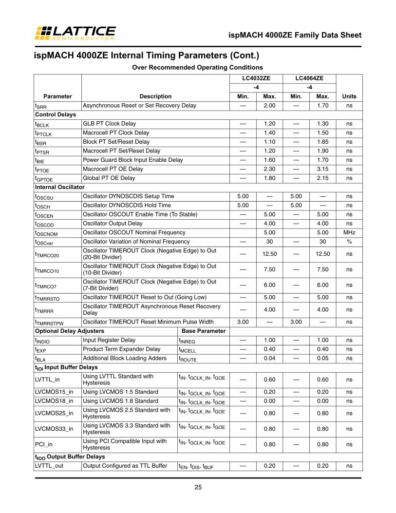
tSRR Asynchronous Reset or Set Recovery Delay — 2.00 — 1.70 ns
Control Delays
tBCLK GLB PT Clock Delay — 1.20 — 1.30 ns
tPTCLK Macrocell PT Clock Delay — 1.40 — 1.50 ns
tBSR Block PT Set/Reset Delay — 1.10 — 1.85 ns
tPTSR Macrocell PT Set/Reset Delay — 1.20 — 1.90 ns
tBIE Power Guard Block Input Enable Delay — 1.60 — 1.70 ns
tPTOE Macrocell PT OE Delay — 2.30 — 3.15 ns
tGPTOE Global PT OE Delay — 1.80 — 2.15 ns
Internal Oscillator
tOSCSU Oscillator DYNOSCDIS Setup Time 5.00 — 5.00 — ns
tOSCH Oscillator DYNOSCDIS Hold Time 5.00 — 5.00 — ns
tOSCEN Oscillator OSCOUT Enable Time (To Stable) — 5.00 — 5.00 ns
tOSCOD Oscillator Output Delay — 4.00 — 4.00 ns
tOSCNOM Oscillator OSCOUT Nominal Frequency 5.00 5.00 MHz
tOSCvar Oscillator Variation of Nominal Frequency — 30 — 30 %
tTMRCO20Oscillator TIMEROUT Clock (Negative Edge) to Out (20-Bit Divider) — 12.50 — 12.50 ns
tTMRCO10Oscillator TIMEROUT Clock (Negative Edge) to Out (10-Bit Divider) — 7.50 — 7.50 ns
tTMRCO7Oscillator TIMEROUT Clock (Negative Edge) to Out (7-Bit Divider) — 6.00 — 6.00 ns
tTMRRSTO Oscillator TIMEROUT Reset to Out (Going Low) — 5.00 — 5.00 ns
tTMRRROscillator TIMEROUT Asynchronous Reset Recovery Delay — 4.00 — 4.00 ns
tTMRRSTPW Oscillator TIMEROUT Reset Minimum Pulse Width 3.00 — 3.00 — ns
Optional Delay Adjusters Base Parameter
tINDIO Input Register Delay tINREG — 1.00 — 1.00 ns
tEXP Product Term Expander Delay tMCELL — 0.40 — 0.40 ns
tBLA Additional Block Loading Adders tROUTE — 0.04 — 0.05 ns
tIOI Input Buffer Delays
LVTTL_in Using LVTTL Standard with Hysteresis
tIN, tGCLK_IN, tGOE — 0.60 — 0.60 ns
LVCMOS15_in Using LVCMOS 1.5 Standard tIN, tGCLK_IN, tGOE — 0.20 — 0.20 ns
LVCMOS18_in Using LVCMOS 1.8 Standard tIN, tGCLK_IN, tGOE — 0.00 — 0.00 ns
LVCMOS25_in Using LVCMOS 2.5 Standard with Hysteresis
tIN, tGCLK_IN, tGOE — 0.80 — 0.80 ns
LVCMOS33_in Using LVCMOS 3.3 Standard with Hysteresis
tIN, tGCLK_IN, tGOE — 0.80 — 0.80 ns
PCI_in Using PCI Compatible Input with Hysteresis
tIN, tGCLK_IN, tGOE — 0.80 — 0.80 ns
tIOO Output Buffer Delays
LVTTL_out Output Configured as TTL Buffer tEN, tDIS, tBUF — 0.20 — 0.20 ns
ispMACH 4000ZE Internal Timing Parameters (Cont.)Over Recommended Operating Conditions
Parameter Description
LC4032ZE LC4064ZE
Units
-4 -4
Min. Max. Min. Max.
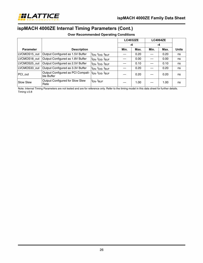
ispMACH 4000ZE Family Data Sheet
26
LVCMOS15_out Output Configured as 1.5V Buffer tEN, tDIS, tBUF — 0.20 — 0.20 ns
LVCMOS18_out Output Configured as 1.8V Buffer tEN, tDIS, tBUF — 0.00 — 0.00 ns
LVCMOS25_out Output Configured as 2.5V Buffer tEN, tDIS, tBUF — 0.10 — 0.10 ns
LVCMOS33_out Output Configured as 3.3V Buffer tEN, tDIS, tBUF — 0.20 — 0.20 ns
PCI_out Output Configured as PCI Compati-ble Buffer
tEN, tDIS, tBUF — 0.20 — 0.20 ns
Slow Slew Output Configured for Slow Slew Rate
tEN, tBUF — 1.00 — 1.00 ns
Note: Internal Timing Parameters are not tested and are for reference only. Refer to the timing model in this data sheet for further details.Timing v.0.8
ispMACH 4000ZE Internal Timing Parameters (Cont.)Over Recommended Operating Conditions
Parameter Description
LC4032ZE LC4064ZE
Units
-4 -4
Min. Max. Min. Max.
ispMACH 4000ZE Family Data Sheet
27
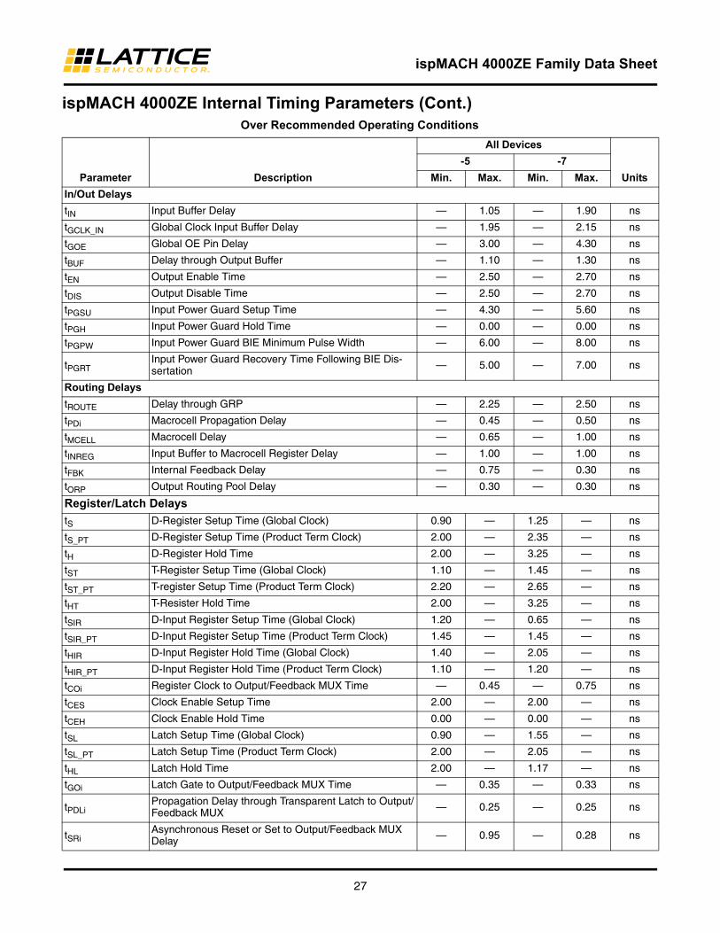
ispMACH 4000ZE Internal Timing Parameters (Cont.)Over Recommended Operating Conditions
Parameter Description
All Devices
Units
-5 -7
Min. Max. Min. Max.
In/Out Delays
tIN Input Buffer Delay — 1.05 — 1.90 ns
tGCLK_IN Global Clock Input Buffer Delay — 1.95 — 2.15 ns
tGOE Global OE Pin Delay — 3.00 — 4.30 ns
tBUF Delay through Output Buffer — 1.10 — 1.30 ns
tEN Output Enable Time — 2.50 — 2.70 ns
tDIS Output Disable Time — 2.50 — 2.70 ns
tPGSU Input Power Guard Setup Time — 4.30 — 5.60 ns
tPGH Input Power Guard Hold Time — 0.00 — 0.00 ns
tPGPW Input Power Guard BIE Minimum Pulse Width — 6.00 — 8.00 ns
tPGRTInput Power Guard Recovery Time Following BIE Dis-sertation — 5.00 — 7.00 ns
Routing Delays
tROUTE Delay through GRP — 2.25 — 2.50 ns
tPDi Macrocell Propagation Delay — 0.45 — 0.50 ns
tMCELL Macrocell Delay — 0.65 — 1.00 ns
tINREG Input Buffer to Macrocell Register Delay — 1.00 — 1.00 ns
tFBK Internal Feedback Delay — 0.75 — 0.30 ns
tORP Output Routing Pool Delay — 0.30 — 0.30 ns
Register/Latch Delays
tS D-Register Setup Time (Global Clock) 0.90 — 1.25 — ns
tS_PT D-Register Setup Time (Product Term Clock) 2.00 — 2.35 — ns
tH D-Register Hold Time 2.00 — 3.25 — ns
tST T-Register Setup Time (Global Clock) 1.10 — 1.45 — ns
tST_PT T-register Setup Time (Product Term Clock) 2.20 — 2.65 — ns
tHT T-Resister Hold Time 2.00 — 3.25 — ns
tSIR D-Input Register Setup Time (Global Clock) 1.20 — 0.65 — ns
tSIR_PT D-Input Register Setup Time (Product Term Clock) 1.45 — 1.45 — ns
tHIR D-Input Register Hold Time (Global Clock) 1.40 — 2.05 — ns
tHIR_PT D-Input Register Hold Time (Product Term Clock) 1.10 — 1.20 — ns
tCOi Register Clock to Output/Feedback MUX Time — 0.45 — 0.75 ns
tCES Clock Enable Setup Time 2.00 — 2.00 — ns
tCEH Clock Enable Hold Time 0.00 — 0.00 — ns
tSL Latch Setup Time (Global Clock) 0.90 — 1.55 — ns
tSL_PT Latch Setup Time (Product Term Clock) 2.00 — 2.05 — ns
tHL Latch Hold Time 2.00 — 1.17 — ns
tGOi Latch Gate to Output/Feedback MUX Time — 0.35 — 0.33 ns
tPDLiPropagation Delay through Transparent Latch to Output/Feedback MUX — 0.25 — 0.25 ns
tSRiAsynchronous Reset or Set to Output/Feedback MUX Delay — 0.95 — 0.28 ns
ispMACH 4000ZE Family Data Sheet
28
tSRR Asynchronous Reset or Set Recovery Delay — 1.80 — 1.67 ns
Control Delays
tBCLK GLB PT Clock Delay — 1.45 — 0.95 ns
tPTCLK Macrocell PT Clock Delay — 1.45 — 1.15 ns
tBSR Block PT Set/Reset Delay — 1.85 — 1.83 ns
tPTSR Macrocell PT Set/Reset Delay — 1.85 — 2.72 ns
tBIE Power Guard Block Input Enable Delay — 1.75 — 1.95 ns
tPTOE Macrocell PT OE Delay — 2.40 — 1.90 ns
tGPTOE Global PT OE Delay — 4.20 — 3.40 ns
Internal Oscillator
tOSCSU Oscillator DYNOSCDIS Setup Time 5.00 — 5.00 — ns
tOSCH Oscillator DYNOSCDIS Hold Time 5.00 — 5.00 — ns
tOSCEN Oscillator OSCOUT Enable Time (To Stable) — 5.00 — 5.00 ns
tOSCOD Oscillator Output Delay — 4.00 — 4.00 ns
tOSCNOM Oscillator OSCOUT Nominal Frequency 5.00 5.00 MHz
tOSCvar Oscillator Variation of Nominal Frequency — 30 — 30 %
tTMRCO20Oscillator TIMEROUT Clock (Negative Edge) to Out (20-Bit Divider) — 12.50 — 14.50 ns
tTMRCO10Oscillator TIMEROUT Clock (Negative Edge) to Out (10-Bit Divider) — 7.50 — 9.50 ns
tTMRCO7Oscillator TIMEROUT Clock (Negative Edge) to Out (7-Bit Divider) — 6.00 — 8.00 ns
tTMRRSTO Oscillator TIMEROUT Reset to Out (Going Low) — 5.00 — 7.00 ns
tTMRRROscillator TIMEROUT Asynchronous Reset Recovery Delay — 4.00 — 6.00 ns
tTMRRSTPW Oscillator TIMEROUT Reset Minimum Pulse Width 3.00 — 5.00 — ns
Optional Delay Adjusters Base Parameter
tINDIO Input Register Delay tINREG — 1.60 — 2.60 ns
tEXP Product Term Expander Delay tMCELL — 0.45 — 0.50 ns
tBLA Additional Block Loading Adders tROUTE — 0.05 — 0.05 ns
tIOI Input Buffer Delays
LVTTL_in Using LVTTL Standard with Hysteresis tIN, tGCLK_IN, tGOE — 0.60 — 0.60 ns
LVCMOS15_in Using LVCMOS 1.5 Standard tIN, tGCLK_IN, tGOE — 0.20 — 0.20 ns
LVCMOS18_in Using LVCMOS 1.8 Standard tIN, tGCLK_IN, tGOE — 0.00 — 0.00 ns
LVCMOS25_in Using LVCMOS 2.5 Standard with Hysteresis tIN, tGCLK_IN, tGOE — 0.80 — 0.80 ns
LVCMOS33_in Using LVCMOS 3.3 Standard with Hysteresis tIN, tGCLK_IN, tGOE — 0.80 — 0.80 ns
PCI_in Using PCI Compatible Input with Hysteresis tIN, tGCLK_IN, tGOE — 0.80 — 0.80 ns
tIOO Output Buffer Delays
LVTTL_out Output Configured as TTL Buffer tEN, tDIS, tBUF — 0.20 — 0.20 ns
ispMACH 4000ZE Internal Timing Parameters (Cont.)Over Recommended Operating Conditions
Parameter Description
All Devices
Units
-5 -7
Min. Max. Min. Max.
ispMACH 4000ZE Family Data Sheet
29
LVCMOS15_out Output Configured as 1.5V Buffer tEN, tDIS, tBUF — 0.20 — 0.20 ns
LVCMOS18_out Output Configured as 1.8V Buffer tEN, tDIS, tBUF — 0.00 — 0.00 ns
LVCMOS25_out Output Configured as 2.5V Buffer tEN, tDIS, tBUF — 0.10 — 0.10 ns
LVCMOS33_out Output Configured as 3.3V Buffer tEN, tDIS, tBUF — 0.20 — 0.20 ns
PCI_out Output Configured as PCI Compati-ble Buffer
tEN, tDIS, tBUF — 0.20 — 0.20 ns
Slow Slew Output Configured for Slow Slew Rate
tEN, tBUF — 1.00 — 1.00 ns
Note: Internal Timing Parameters are not tested and are for reference only. Refer to the timing model in this data sheet for further details.Timing v.0.8
ispMACH 4000ZE Internal Timing Parameters (Cont.)Over Recommended Operating Conditions
Parameter Description
All Devices
Units
-5 -7
Min. Max. Min. Max.
ispMACH 4000ZE Family Data Sheet
30
Boundary Scan Waveforms and Timing Specifications
Symbol Parameter Min. Max. Units
tBTCP TCK [BSCAN test] clock cycle 40 — ns
tBTCH TCK [BSCAN test] pulse width high 20 — ns
tBTCL TCK [BSCAN test] pulse width low 20 — ns
tBTSU TCK [BSCAN test] setup time 8 — ns
tBTH TCK [BSCAN test] hold time 10 — ns
tBRF TCK [BSCAN test] rise and fall time 50 — mV/ns
tBTCO TAP controller falling edge of clock to valid output — 10 ns
tBTOZ TAP controller falling edge of clock to data output disable — 10 ns
tBTVO TAP controller falling edge of clock to data output enable — 10 ns
tBTCPSU BSCAN test Capture register setup time 8 — ns
tBTCPH BSCAN test Capture register hold time 10 — ns
tBTUCO BSCAN test Update reg, falling edge of clock to valid output — 25 ns
tBTUOZ BSCAN test Update reg, falling edge of clock to output disable — 25 ns
tBTUOV BSCAN test Update reg, falling edge of clock to output enable — 25 ns
ispMACH 4000ZE Family Data Sheet
31
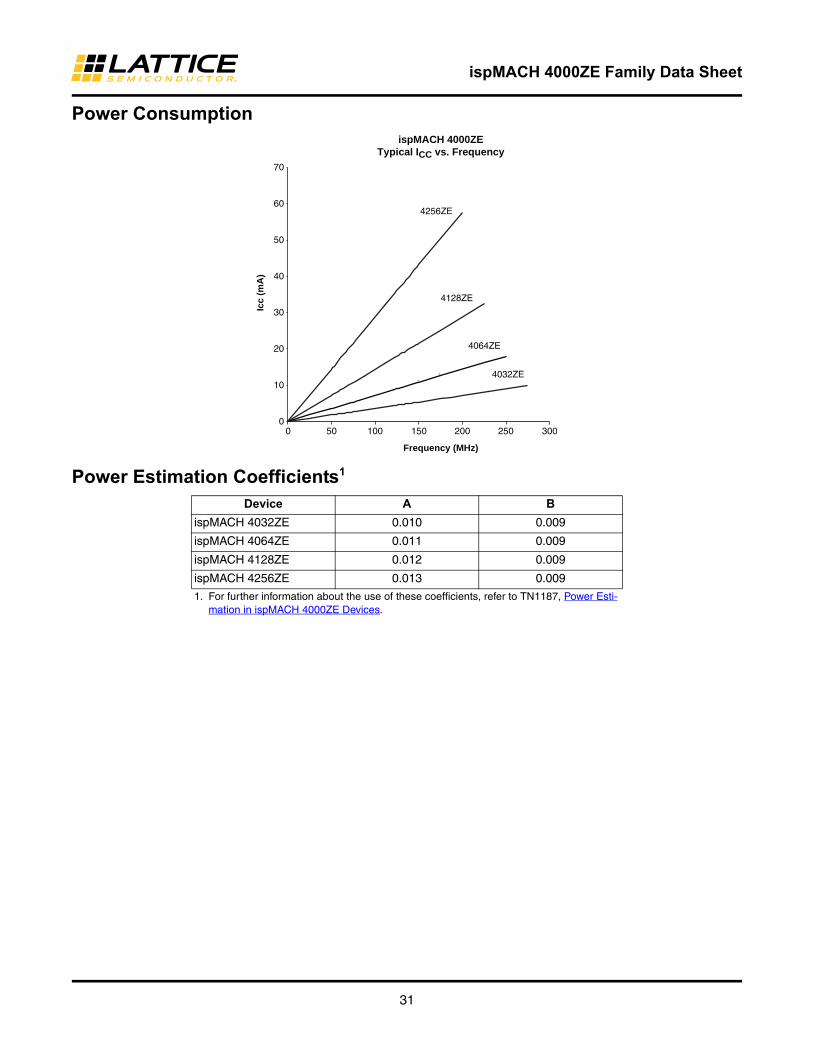
Power Consumption
Power Estimation Coefficients1
Device A B
ispMACH 4032ZE 0.010 0.009
ispMACH 4064ZE 0.011 0.009
ispMACH 4128ZE 0.012 0.009
ispMACH 4256ZE 0.013 0.009
1. For further information about the use of these coefficients, refer to TN1187, Power Esti-mation in ispMACH 4000ZE Devices.
4032ZE
4064ZE
4128ZE
4256ZE
ispMACH 4000ZETypical ICC vs. Frequency
00 50 100 150 200 250 300
10
20
30
40
50
60
70
Frequency (MHz)
Icc
(mA
)
ispMACH 4000ZE Family Data Sheet
32
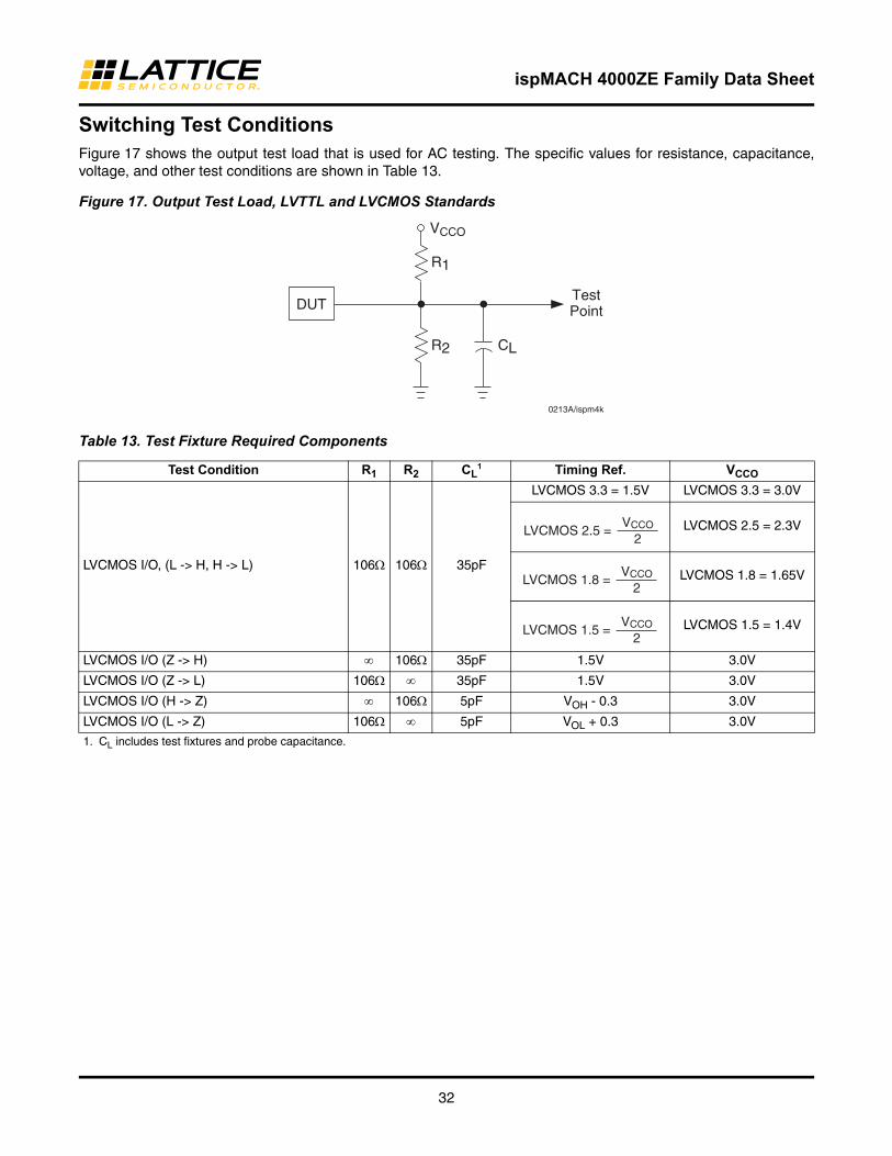
Switching Test ConditionsFigure 17 shows the output test load that is used for AC testing. The specific values for resistance, capacitance,voltage, and other test conditions are shown in Table 13.
Figure 17. Output Test Load, LVTTL and LVCMOS Standards
Table 13. Test Fixture Required Components
Test Condition R1 R2 CL1 Timing Ref. VCCO
LVCMOS I/O, (L -> H, H -> L) 106 106 35pF
LVCMOS 3.3 = 1.5V LVCMOS 3.3 = 3.0V
LVCMOS 2.5 = 2.3V
LVCMOS 1.8 = 1.65V
LVCMOS 1.5 = 1.4V
LVCMOS I/O (Z -> H) 106 35pF 1.5V 3.0V
LVCMOS I/O (Z -> L) 106 35pF 1.5V 3.0V
LVCMOS I/O (H -> Z) 106 5pF VOH - 0.3 3.0V
LVCMOS I/O (L -> Z) 106 5pF VOL + 0.3 3.0V
1. CL includes test fixtures and probe capacitance.
VCCO
R1
R2 CL
DUTTestPoint
0213A/ispm4k
LVCMOS 2.5 = VCCO
2
LVCMOS 1.8 = VCCO
2
LVCMOS 1.5 = VCCO
2
ispMACH 4000ZE Family Data Sheet
33
Signal Descriptions
ORP Reference Table
Signal Names Description
TMS Input – This pin is the IEEE 1149.1 Test Mode Select input, which is used to control the state machine.
TCK Input – This pin is the IEEE 1149.1 Test Clock input pin, used to clock through the state machine.
TDI Input – This pin is the IEEE 1149.1 Test Data In pin, used to load data.
TDO Output – This pin is the IEEE 1149.1 Test Data Out pin used to shift data out.
GOE0/IO, GOE1/IO These pins are configured to be either Global Output Enable Input or as general I/O pins.
GND Ground
NC Not Connected
VCC The power supply pins for logic core and JTAG port.
CLK0/I, CLK1/I, CLK2/I, CLK3/I These pins are configured to be either CLK input or as an input.
VCCO0, VCCO1 The power supply pins for each I/O bank.
yzz
Input/Output1 – These are the general purpose I/O used by the logic array. y is GLB reference (alpha) and z is macrocell reference (numeric). z: 0-15.
ispMACH 4032ZE y: A-B
ispMACH 4064ZE y: A-D
ispMACH 4128ZE y: A-H
ispMACH 4256ZE y: A-P
1. In some packages, certain I/Os are only available for use as inputs. See the Logic Signal Connections tables for details.
4032ZE 4064ZE 4128ZE 4256ZE
Number of I/Os 32 32 48 64 64 96 64 96 108
Number of GLBs 2 4 4 4 8 8 16 16 16
Number of I/Os per GLB
16 8 Mixture of 9, 10, 14, 15
16 8 12 4 6 Mixture of 6, 7, 8
Reference ORP Table (I/Os per GLB)
16 8 9, 10, 14, 15
16 8 12 4 6 6, 7, 8
ispMACH 4000ZE Family Data Sheet
34
ispMACH 4000ZE Power Supply and NC Connections1
Signal 48 TQFP2 64 csBGA3, 4 64 ucBGA3, 4 100 TQFP2
VCC 12, 36 E4, D5 E4, D5 25, 40, 75, 90
VCCO0VCCO (Bank 0)
6 4032ZE: E34064ZE: E3, F4
C3, F3 13, 33, 95
VCCO1VCCO (Bank 1)
30 4032ZE: D64064ZE: D6, C6
F6, A6 45, 63, 83
GND 13, 37 D4, E5 D4, D5 1, 26, 51, 76
GND (Bank 0) 5 D4, E5 D4, D5 7, 18, 32, 96
GND (Bank 1) 29 D4, E5 D4, D5 46, 57, 68, 82
NC — — — —
1. All grounds must be electrically connected at the board level. However, for the purposes of I/O current loading, grounds are associated with the bank shown.
2. Pin orientation follows the conventional order from pin 1 marking of the top side view and counter-clockwise.3. Pin orientation A1 starts from the upper left corner of the top side view with alphabetical order ascending vertically and numerical order
ascending horizontally.4. All bonded grounds are connected to the following two balls, D4 and E5.
ispMACH 4000ZE Family Data Sheet
35
ispMACH 4000ZE Power Supply and NC Connections1 (Cont.)
Signal 132 ucBGA3 144 csBGA3 144 TQFP2
VCC M1, M7, A12, B5 H5, H8, E8, E5 36, 57, 108, 129
VCCO0 VCCO (Bank 0)
B1, H4, L2, J5, A4 E4, F4, G4, J5, D5 3, 19, 34, 47, 136
VCCO1VCCO (Bank 1)
K9, L12, F12, D9, C7 J8, H9, G9, F9, D8 64, 75, 91, 106, 119
GND E5, E8, H5, H8 F6, G6, G7, F7 1, 37, 73, 109
GND (Bank 0) E2, H2, M4, B7, B3 G5, H4, H6, E6, F5 10, 184, 27, 46, 127, 137
GND (Bank 1) L7, J9, H12, E9, A9 H7, J9, G8, F8, E7 55, 65, 82, 904, 99, 118
NC — 4064ZE: E4, B2, B1, D2, D3, E1, H1, H3, H2, L1, G4, M1, K3, M2, M4, L5, H7, L8, M8, L10, K9, M11, H9, L12, L11, J12, J11, H10, D10, F10, D12, B12, F9, A12, C10, B10, A9, B8, E6, B5, A5, C4, B3, A24128ZE: D2, D3, H2, M1, K3, M11, J12, J11, D12, A12, C10, A2
4128ZE: 17, 20, 38, 45, 72, 89, 92, 110, 117, 1444256ZE: 18, 90
1. All grounds must be electrically connected at the board level. However, for the purposes of I/O current loading, grounds are associated with the bank shown.
2. Pin orientation follows the conventional order from pin 1 marking of the top side view and counter-clockwise.3. Pin orientation A1 starts from the upper left corner of the top side view with alphabetical order ascending vertically and numerical order
ascending horizontally.4. For the LC4256ZE, pins 18 and 90 are no connects.
ispMACH 4000ZE Family Data Sheet
36
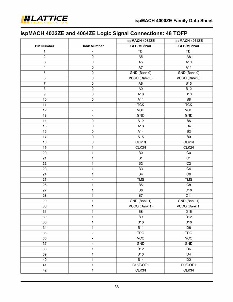
ispMACH 4032ZE and 4064ZE Logic Signal Connections: 48 TQFP
Pin Number Bank Number
ispMACH 4032ZE ispMACH 4064ZE
GLB/MC/Pad GLB/MC/Pad
1 - TDI TDI
2 0 A5 A8
3 0 A6 A10
4 0 A7 A11
5 0 GND (Bank 0) GND (Bank 0)
6 0 VCCO (Bank 0) VCCO (Bank 0)
7 0 A8 B15
8 0 A9 B12
9 0 A10 B10
10 0 A11 B8
11 - TCK TCK
12 - VCC VCC
13 - GND GND
14 0 A12 B6
15 0 A13 B4
16 0 A14 B2
17 0 A15 B0
18 0 CLK1/I CLK1/I
19 1 CLK2/I CLK2/I
20 1 B0 C0
21 1 B1 C1
22 1 B2 C2
23 1 B3 C4
24 1 B4 C6
25 - TMS TMS
26 1 B5 C8
27 1 B6 C10
28 1 B7 C11
29 1 GND (Bank 1) GND (Bank 1)
30 1 VCCO (Bank 1) VCCO (Bank 1)
31 1 B8 D15
32 1 B9 D12
33 1 B10 D10
34 1 B11 D8
35 - TDO TDO
36 - VCC VCC
37 - GND GND
38 1 B12 D6
39 1 B13 D4
40 1 B14 D2
41 1 B15/GOE1 D0/GOE1
42 1 CLK3/I CLK3/I

ispMACH 4000ZE Family Data Sheet
37
43 0 CLK0/I CLK0/I
44 0 A0/GOE0 A0/GOE0
45 0 A1 A1
46 0 A2 A2
47 0 A3 A4
48 0 A4 A6
ispMACH 4032ZE and 4064ZE Logic Signal Connections: 48 TQFP (Cont.)
Pin Number Bank Number
ispMACH 4032ZE ispMACH 4064ZE
GLB/MC/Pad GLB/MC/Pad

ispMACH 4000ZE Family Data Sheet
38
ispMACH 4032ZE and 4064ZE Logic Signal Connections: 64 csBGA
Ball Number Bank Number
ispMACH 4032ZE ispMACH 4064ZE
GLB/MC/Pad GLB/MC/Pad
B2 - TDI TDI
B1 0 A5 A8
C2 0 A6 A10
C1 0 A7 A11
GND* 0 GND (Bank 0) GND (Bank 0)
C3 0 NC A12
E3 0 VCCO (Bank 0) VCCO (Bank 0)
D1 0 A8 B15
D2 0 NC B14
E1 0 A9 B13
D3 0 A10 B12
F1 0 A11 B11
E2 0 NC B10
G1 0 NC B9
F2 0 NC B8
H1 - TCK TCK
E4 - VCC VCC
GND* - GND GND
G2 0 A12 B6
H2 0 NC B5
H3 0 A13 B4
GND* 0 NC GND (Bank 0)
F4 0 NC VCCO (Bank 0)
G3 0 A14 B3
F3 0 NC B2
H4 0 A15 B0
G4 0 CLK1/I CLK1/I
H5 1 CLK2/I CLK2/I
F5 1 B0 C0
G5 1 B1 C1
G6 1 B2 C2
H6 1 B3 C4
F6 1 B4 C5
H7 1 NC C6
H8 - TMS TMS
G7 1 B5 C8
F7 1 B6 C10
G8 1 B7 C11
GND* 1 GND (Bank 0) GND (Bank 1)
F8 1 NC C12
D6 1 VCCO (Bank 1) VCCO (Bank 1)
E8 1 B8 D15
ispMACH 4000ZE Family Data Sheet
39
E7 1 NC D14
E6 1 B9 D13
D7 1 B10 D12
D8 1 NC D11
C5 1 NC D10
C7 1 B11 D9
C8 1 NC D8
B8 - TDO TDO
D5 - VCC VCC
GND* - GND GND
A8 1 B12 D7
A7 1 NC D6
B7 1 NC D5
A6 1 B13 D4
GND* 1 NC GND (Bank 1)
C6 1 NC VCCO (Bank 1)
B6 1 B14 D3
A5 1 NC D2
B5 1 B15/GOE1 D0/GOE1
A4 1 CLK3/I CLK3/I
C4 0 CLK0/I CLK0/I
B4 0 A0/GOE0 A0/GOE0
B3 0 A1 A1
A3 0 A2 A2
A2 0 A3 A4
A1 0 A4 A6
* All bonded grounds are connected to the following two balls, D4 and E5.
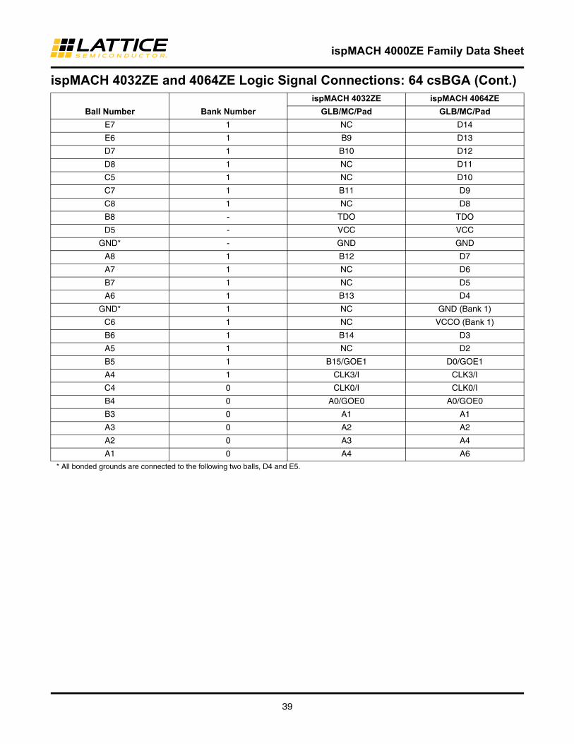
ispMACH 4032ZE and 4064ZE Logic Signal Connections: 64 csBGA (Cont.)
Ball Number Bank Number
ispMACH 4032ZE ispMACH 4064ZE
GLB/MC/Pad GLB/MC/Pad

ispMACH 4000ZE Family Data Sheet
40
ispMACH 4064ZE Logic Signal Connections: 64 ucBGABall Number Bank Number GLB/MC/Pad
A1 - TDI
B1 0 A8
B2 0 A10
B3 0 A11
GND* 0 GND (Bank 0)
C1 0 A12
C3 0 VCCO (Bank 0)
C2 0 B15
D1 0 B14
D2 0 B13
D3 0 B12
E1 0 B11
E2 0 B10
E3 0 B9
F1 0 B8
F2 - TCK
E4 - VCC
GND* - GND
H2 0 B6
H1 0 B5
G1 0 B4
GND* 0 GND (Bank 0)
F3 0 VCCO (Bank 0)
G2 0 B3
G3 0 B2
H3 0 B0
G4 0 CLK1/I
F4 1 CLK2/I
H4 1 C0
H5 1 C1
G5 1 C2
H6 1 C4
H7 1 C5
H8 1 C6
G8 - TMS
G7 1 C8
G6 1 C10
F8 1 C11
GND* 1 GND (Bank 1)
F7 1 C12
F6 1 VCCO (Bank 1)
F5 1 D15
E8 1 D14
ispMACH 4000ZE Family Data Sheet
41
E7 1 D13
E6 1 D12
D8 1 D11
D7 1 D10
D6 1 D9
C8 1 D8
C7 - TDO
D5 - VCC
GND* - GND
B8 1 D7
A8 1 D6
B7 1 D5
A7 1 D4
GND* 1 GND (Bank 1)
A6 1 VCCO (Bank 1)
B6 1 D3
C6 1 D2
A5 1 D0/GOE1
B5 1 CLK3/I
C5 0 CLK0/I
A4 0 A0/GOE0
B4 0 A1
C4 0 A2
A3 0 A4
A2 0 A6
* All bonded grounds are connected to the following two balls, D4 and E5.
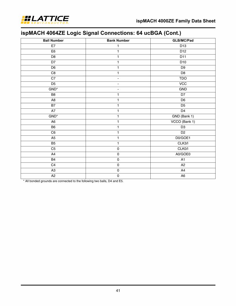
ispMACH 4064ZE Logic Signal Connections: 64 ucBGA (Cont.)Ball Number Bank Number GLB/MC/Pad
ispMACH 4000ZE Family Data Sheet
42
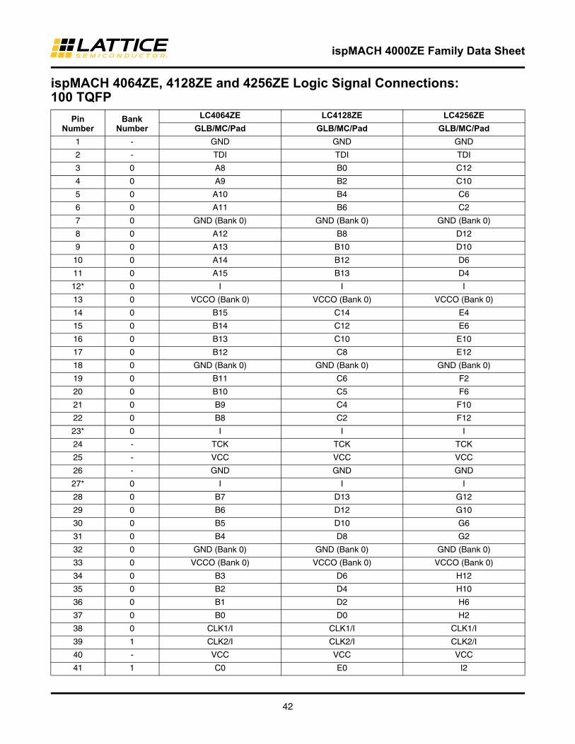
ispMACH 4064ZE, 4128ZE and 4256ZE Logic Signal Connections: 100 TQFP
Pin Number
Bank Number
LC4064ZE LC4128ZE LC4256ZE
GLB/MC/Pad GLB/MC/Pad GLB/MC/Pad
1 - GND GND GND
2 - TDI TDI TDI
3 0 A8 B0 C12
4 0 A9 B2 C10
5 0 A10 B4 C6
6 0 A11 B6 C2
7 0 GND (Bank 0) GND (Bank 0) GND (Bank 0)
8 0 A12 B8 D12
9 0 A13 B10 D10
10 0 A14 B12 D6
11 0 A15 B13 D4
12* 0 I I I
13 0 VCCO (Bank 0) VCCO (Bank 0) VCCO (Bank 0)
14 0 B15 C14 E4
15 0 B14 C12 E6
16 0 B13 C10 E10
17 0 B12 C8 E12
18 0 GND (Bank 0) GND (Bank 0) GND (Bank 0)
19 0 B11 C6 F2
20 0 B10 C5 F6
21 0 B9 C4 F10
22 0 B8 C2 F12
23* 0 I I I
24 - TCK TCK TCK
25 - VCC VCC VCC
26 - GND GND GND
27* 0 I I I
28 0 B7 D13 G12
29 0 B6 D12 G10
30 0 B5 D10 G6
31 0 B4 D8 G2
32 0 GND (Bank 0) GND (Bank 0) GND (Bank 0)
33 0 VCCO (Bank 0) VCCO (Bank 0) VCCO (Bank 0)
34 0 B3 D6 H12
35 0 B2 D4 H10
36 0 B1 D2 H6
37 0 B0 D0 H2
38 0 CLK1/I CLK1/I CLK1/I
39 1 CLK2/I CLK2/I CLK2/I
40 - VCC VCC VCC
41 1 C0 E0 I2

ispMACH 4000ZE Family Data Sheet
43
42 1 C1 E2 I6
43 1 C2 E4 I10
44 1 C3 E6 I12
45 1 VCCO (Bank 1) VCCO (Bank 1) VCCO (Bank 1)
46 1 GND (Bank 1) GND (Bank 1) GND (Bank 1)
47 1 C4 E8 J2
48 1 C5 E10 J6
49 1 C6 E12 J10
50 1 C7 E14 J12
51 - GND GND GND
52 - TMS TMS TMS
53 1 C8 F0 K12
54 1 C9 F2 K10
55 1 C10 F4 K6
56 1 C11 F6 K2
57 1 GND (Bank 1) GND (Bank 1) GND (Bank 1)
58 1 C12 F8 L12
59 1 C13 F10 L10
60 1 C14 F12 L6
61 1 C15 F13 L4
62* 1 I I I
63 1 VCCO (Bank 1) VCCO (Bank 1) VCCO (Bank 1)
64 1 D15 G14 M4
65 1 D14 G12 M6
66 1 D13 G10 M10
67 1 D12 G8 M12
68 1 GND (Bank 1) GND (Bank 1) GND (Bank 1)
69 1 D11 G6 N2
70 1 D10 G5 N6
71 1 D9 G4 N10
72 1 D8 G2 N12
73* 1 I I I
74 - TDO TDO TDO
75 - VCC VCC VCC
76 - GND GND GND
77* 1 I I I
78 1 D7 H13 O12
79 1 D6 H12 O10
80 1 D5 H10 O6
81 1 D4 H8 O2
82 1 GND (Bank 1) GND (Bank 1) GND (Bank 1)
ispMACH 4064ZE, 4128ZE and 4256ZE Logic Signal Connections: 100 TQFP (Cont.)
Pin Number
Bank Number
LC4064ZE LC4128ZE LC4256ZE
GLB/MC/Pad GLB/MC/Pad GLB/MC/Pad
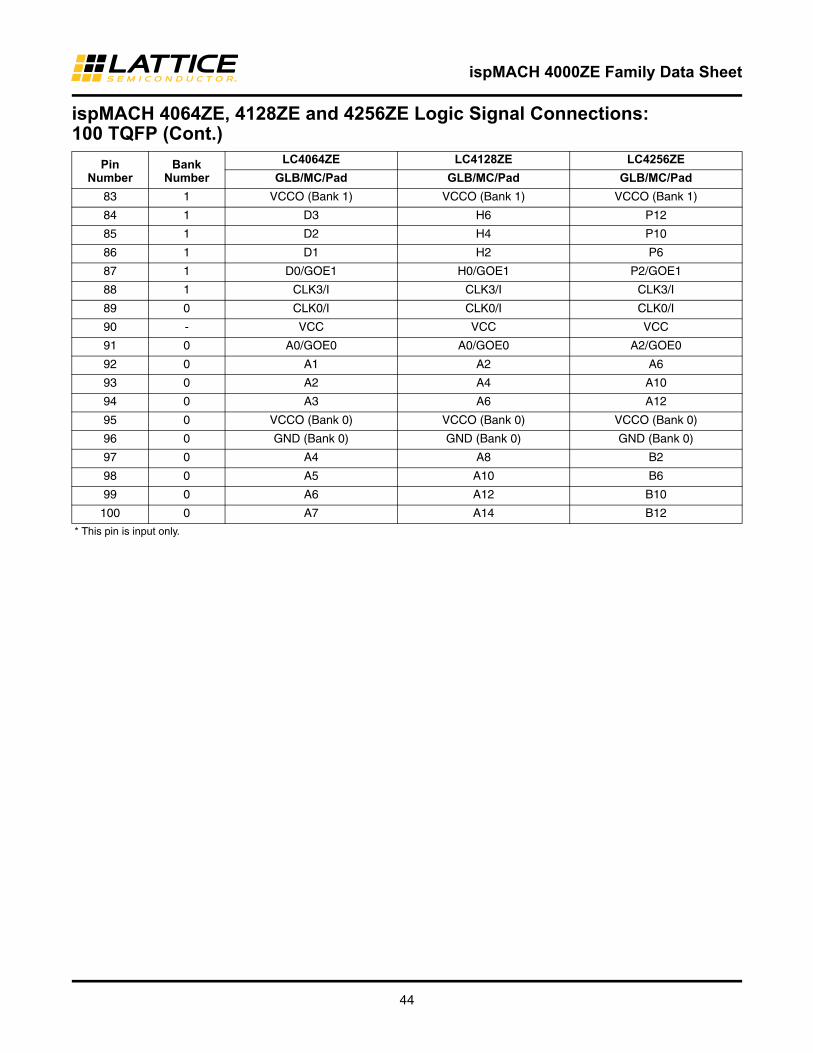
ispMACH 4000ZE Family Data Sheet
44
83 1 VCCO (Bank 1) VCCO (Bank 1) VCCO (Bank 1)
84 1 D3 H6 P12
85 1 D2 H4 P10
86 1 D1 H2 P6
87 1 D0/GOE1 H0/GOE1 P2/GOE1
88 1 CLK3/I CLK3/I CLK3/I
89 0 CLK0/I CLK0/I CLK0/I
90 - VCC VCC VCC
91 0 A0/GOE0 A0/GOE0 A2/GOE0
92 0 A1 A2 A6
93 0 A2 A4 A10
94 0 A3 A6 A12
95 0 VCCO (Bank 0) VCCO (Bank 0) VCCO (Bank 0)
96 0 GND (Bank 0) GND (Bank 0) GND (Bank 0)
97 0 A4 A8 B2
98 0 A5 A10 B6
99 0 A6 A12 B10
100 0 A7 A14 B12
* This pin is input only.
ispMACH 4064ZE, 4128ZE and 4256ZE Logic Signal Connections: 100 TQFP (Cont.)
Pin Number
Bank Number
LC4064ZE LC4128ZE LC4256ZE
GLB/MC/Pad GLB/MC/Pad GLB/MC/Pad
ispMACH 4000ZE Family Data Sheet
45
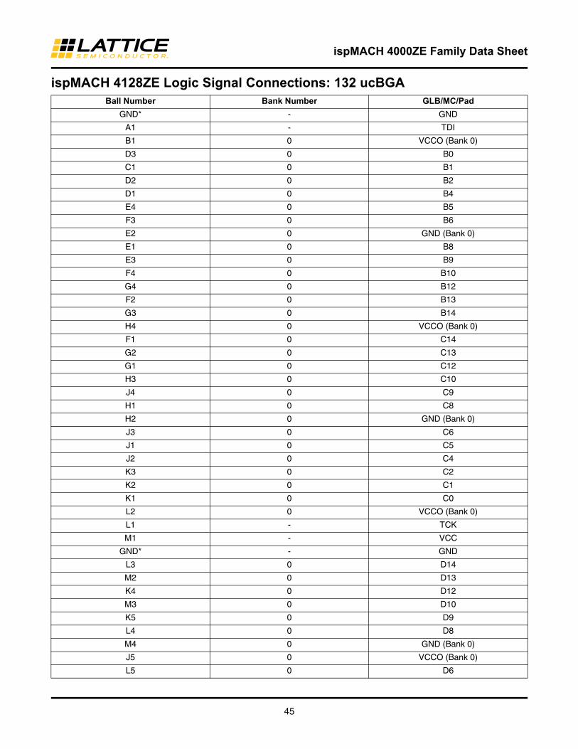
ispMACH 4128ZE Logic Signal Connections: 132 ucBGABall Number Bank Number GLB/MC/Pad
GND* - GND
A1 - TDI
B1 0 VCCO (Bank 0)
D3 0 B0
C1 0 B1
D2 0 B2
D1 0 B4
E4 0 B5
F3 0 B6
E2 0 GND (Bank 0)
E1 0 B8
E3 0 B9
F4 0 B10
G4 0 B12
F2 0 B13
G3 0 B14
H4 0 VCCO (Bank 0)
F1 0 C14
G2 0 C13
G1 0 C12
H3 0 C10
J4 0 C9
H1 0 C8
H2 0 GND (Bank 0)
J3 0 C6
J1 0 C5
J2 0 C4
K3 0 C2
K2 0 C1
K1 0 C0
L2 0 VCCO (Bank 0)
L1 - TCK
M1 - VCC
GND* - GND
L3 0 D14
M2 0 D13
K4 0 D12
M3 0 D10
K5 0 D9
L4 0 D8
M4 0 GND (Bank 0)
J5 0 VCCO (Bank 0)
L5 0 D6
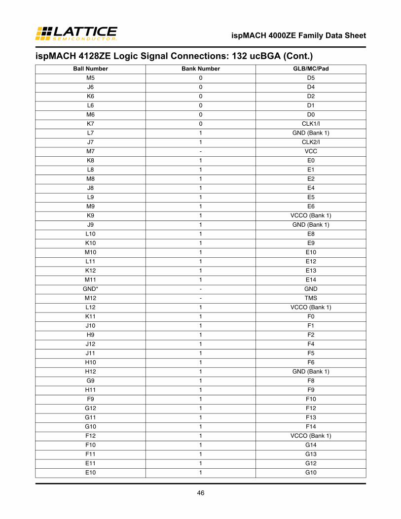
ispMACH 4000ZE Family Data Sheet
46
M5 0 D5
J6 0 D4
K6 0 D2
L6 0 D1
M6 0 D0
K7 0 CLK1/I
L7 1 GND (Bank 1)
J7 1 CLK2/I
M7 - VCC
K8 1 E0
L8 1 E1
M8 1 E2
J8 1 E4
L9 1 E5
M9 1 E6
K9 1 VCCO (Bank 1)
J9 1 GND (Bank 1)
L10 1 E8
K10 1 E9
M10 1 E10
L11 1 E12
K12 1 E13
M11 1 E14
GND* - GND
M12 - TMS
L12 1 VCCO (Bank 1)
K11 1 F0
J10 1 F1
H9 1 F2
J12 1 F4
J11 1 F5
H10 1 F6
H12 1 GND (Bank 1)
G9 1 F8
H11 1 F9
F9 1 F10
G12 1 F12
G11 1 F13
G10 1 F14
F12 1 VCCO (Bank 1)
F10 1 G14
F11 1 G13
E11 1 G12
E10 1 G10
ispMACH 4128ZE Logic Signal Connections: 132 ucBGA (Cont.)Ball Number Bank Number GLB/MC/Pad
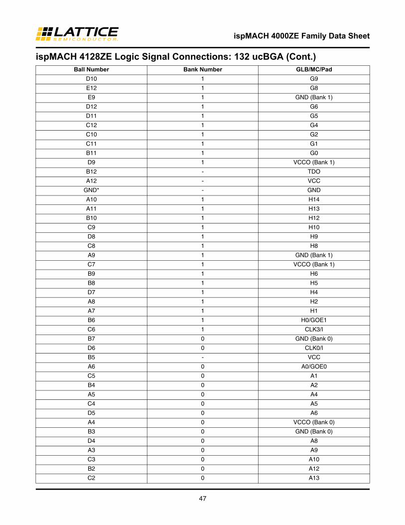
ispMACH 4000ZE Family Data Sheet
47
D10 1 G9
E12 1 G8
E9 1 GND (Bank 1)
D12 1 G6
D11 1 G5
C12 1 G4
C10 1 G2
C11 1 G1
B11 1 G0
D9 1 VCCO (Bank 1)
B12 - TDO
A12 - VCC
GND* - GND
A10 1 H14
A11 1 H13
B10 1 H12
C9 1 H10
D8 1 H9
C8 1 H8
A9 1 GND (Bank 1)
C7 1 VCCO (Bank 1)
B9 1 H6
B8 1 H5
D7 1 H4
A8 1 H2
A7 1 H1
B6 1 H0/GOE1
C6 1 CLK3/I
B7 0 GND (Bank 0)
D6 0 CLK0/I
B5 - VCC
A6 0 A0/GOE0
C5 0 A1
B4 0 A2
A5 0 A4
C4 0 A5
D5 0 A6
A4 0 VCCO (Bank 0)
B3 0 GND (Bank 0)
D4 0 A8
A3 0 A9
C3 0 A10
B2 0 A12
C2 0 A13
ispMACH 4128ZE Logic Signal Connections: 132 ucBGA (Cont.)Ball Number Bank Number GLB/MC/Pad
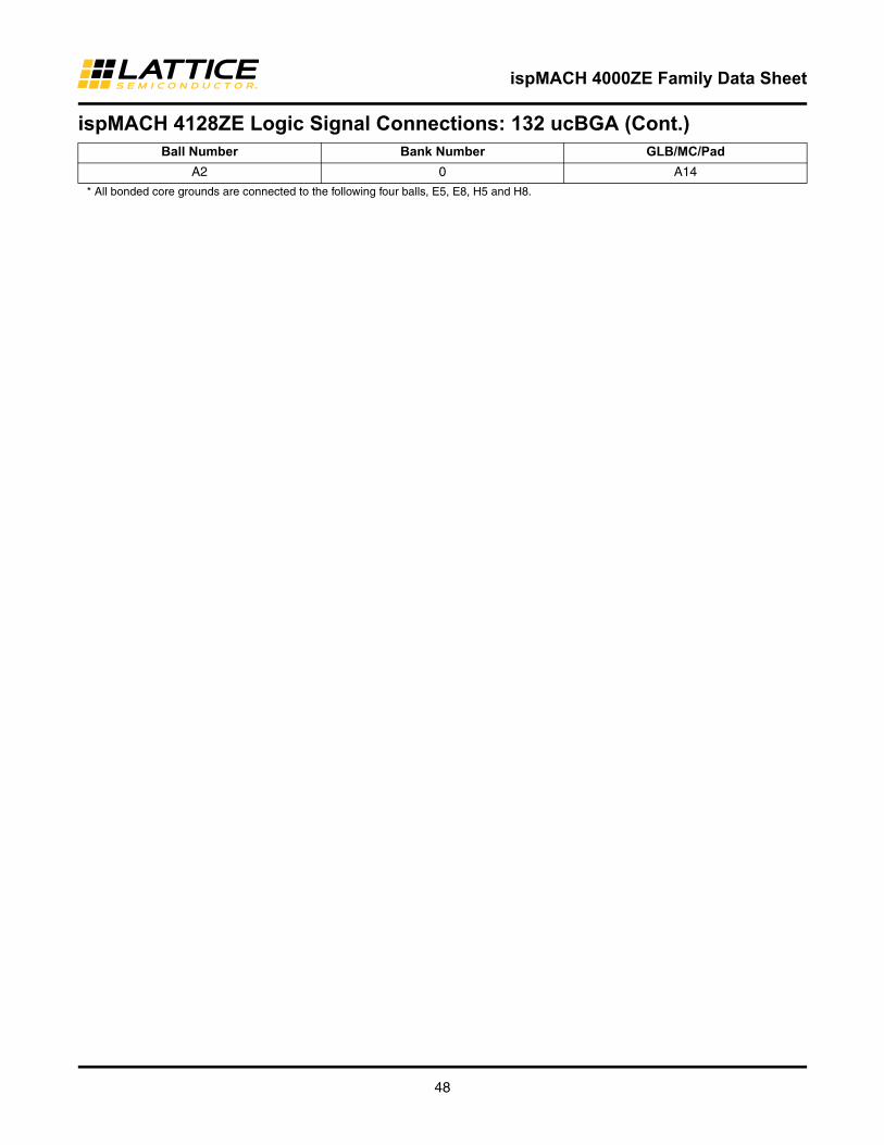
ispMACH 4000ZE Family Data Sheet
48
A2 0 A14
* All bonded core grounds are connected to the following four balls, E5, E8, H5 and H8.
ispMACH 4128ZE Logic Signal Connections: 132 ucBGA (Cont.)Ball Number Bank Number GLB/MC/Pad
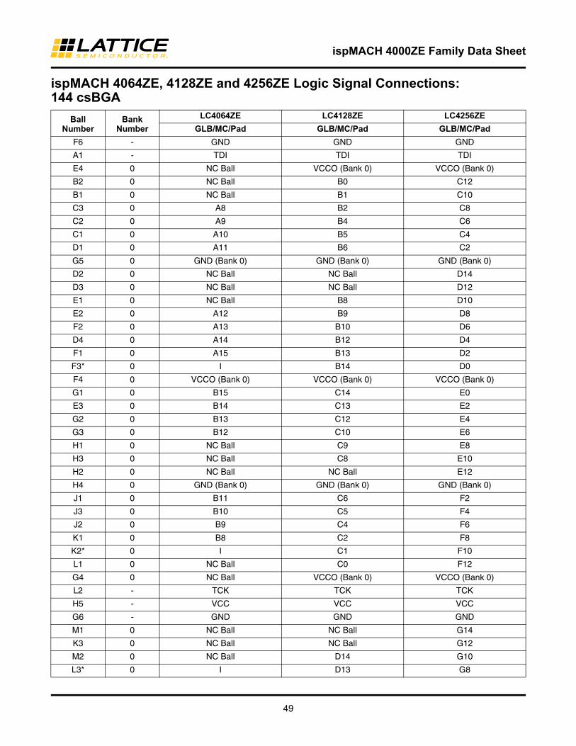
ispMACH 4000ZE Family Data Sheet
49
ispMACH 4064ZE, 4128ZE and 4256ZE Logic Signal Connections: 144 csBGA
BallNumber
BankNumber
LC4064ZE LC4128ZE LC4256ZE
GLB/MC/Pad GLB/MC/Pad GLB/MC/Pad
F6 - GND GND GND
A1 - TDI TDI TDI
E4 0 NC Ball VCCO (Bank 0) VCCO (Bank 0)
B2 0 NC Ball B0 C12
B1 0 NC Ball B1 C10
C3 0 A8 B2 C8
C2 0 A9 B4 C6
C1 0 A10 B5 C4
D1 0 A11 B6 C2
G5 0 GND (Bank 0) GND (Bank 0) GND (Bank 0)
D2 0 NC Ball NC Ball D14
D3 0 NC Ball NC Ball D12
E1 0 NC Ball B8 D10
E2 0 A12 B9 D8
F2 0 A13 B10 D6
D4 0 A14 B12 D4
F1 0 A15 B13 D2
F3* 0 I B14 D0
F4 0 VCCO (Bank 0) VCCO (Bank 0) VCCO (Bank 0)
G1 0 B15 C14 E0
E3 0 B14 C13 E2
G2 0 B13 C12 E4
G3 0 B12 C10 E6
H1 0 NC Ball C9 E8
H3 0 NC Ball C8 E10
H2 0 NC Ball NC Ball E12
H4 0 GND (Bank 0) GND (Bank 0) GND (Bank 0)
J1 0 B11 C6 F2
J3 0 B10 C5 F4
J2 0 B9 C4 F6
K1 0 B8 C2 F8
K2* 0 I C1 F10
L1 0 NC Ball C0 F12
G4 0 NC Ball VCCO (Bank 0) VCCO (Bank 0)
L2 - TCK TCK TCK
H5 - VCC VCC VCC
G6 - GND GND GND
M1 0 NC Ball NC Ball G14
K3 0 NC Ball NC Ball G12
M2 0 NC Ball D14 G10
L3* 0 I D13 G8
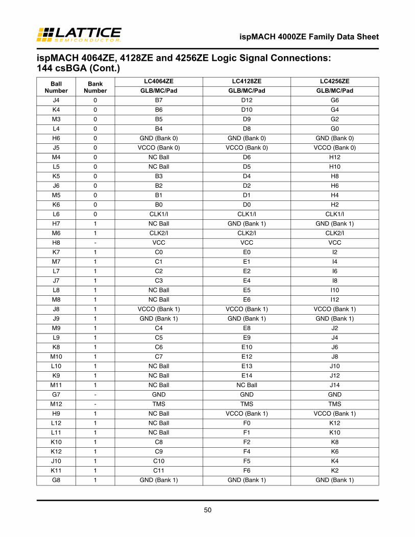
ispMACH 4000ZE Family Data Sheet
50
J4 0 B7 D12 G6
K4 0 B6 D10 G4
M3 0 B5 D9 G2
L4 0 B4 D8 G0
H6 0 GND (Bank 0) GND (Bank 0) GND (Bank 0)
J5 0 VCCO (Bank 0) VCCO (Bank 0) VCCO (Bank 0)
M4 0 NC Ball D6 H12
L5 0 NC Ball D5 H10
K5 0 B3 D4 H8
J6 0 B2 D2 H6
M5 0 B1 D1 H4
K6 0 B0 D0 H2
L6 0 CLK1/I CLK1/I CLK1/I
H7 1 NC Ball GND (Bank 1) GND (Bank 1)
M6 1 CLK2/I CLK2/I CLK2/I
H8 - VCC VCC VCC
K7 1 C0 E0 I2
M7 1 C1 E1 I4
L7 1 C2 E2 I6
J7 1 C3 E4 I8
L8 1 NC Ball E5 I10
M8 1 NC Ball E6 I12
J8 1 VCCO (Bank 1) VCCO (Bank 1) VCCO (Bank 1)
J9 1 GND (Bank 1) GND (Bank 1) GND (Bank 1)
M9 1 C4 E8 J2
L9 1 C5 E9 J4
K8 1 C6 E10 J6
M10 1 C7 E12 J8
L10 1 NC Ball E13 J10
K9 1 NC Ball E14 J12
M11 1 NC Ball NC Ball J14
G7 - GND GND GND
M12 - TMS TMS TMS
H9 1 NC Ball VCCO (Bank 1) VCCO (Bank 1)
L12 1 NC Ball F0 K12
L11 1 NC Ball F1 K10
K10 1 C8 F2 K8
K12 1 C9 F4 K6
J10 1 C10 F5 K4
K11 1 C11 F6 K2
G8 1 GND (Bank 1) GND (Bank 1) GND (Bank 1)
ispMACH 4064ZE, 4128ZE and 4256ZE Logic Signal Connections: 144 csBGA (Cont.)
BallNumber
BankNumber
LC4064ZE LC4128ZE LC4256ZE
GLB/MC/Pad GLB/MC/Pad GLB/MC/Pad

ispMACH 4000ZE Family Data Sheet
51
J12 1 NC Ball NC Ball L14
J11 1 NC Ball NC Ball L12
H10 1 NC Ball F8 L10
H12 1 C12 F9 L8
G11 1 C13 F10 L6
H11 1 C14 F12 L4
G12 1 C15 F13 L2
G10* 1 I F14 L0
G9 1 VCCO (Bank 1) VCCO (Bank 1) VCCO (Bank 1)
F12 1 D15 G14 M0
F11 1 D14 G13 M2
E11 1 D13 G12 M4
E12 1 D12 G10 M6
D10 1 NC Ball G9 M8
F10 1 NC Ball G8 M10
D12 1 NC Ball NC Ball M12
F8 1 GND (Bank 1) GND (Bank 1) GND (Bank 1)
E10 1 D11 G6 N2
D11 1 D10 G5 N4
E9 1 D9 G4 N6
C12 1 D8 G2 N8
C11* 1 I G1 N10
B12 1 NC Ball G0 N12
F9 1 NC Ball VCCO (Bank 1) VCCO (Bank 1)
B11 - TDO TDO TDO
E8 - VCC VCC VCC
F7 - GND GND GND
A12 1 NC Ball NC Ball O14
C10 1 NC Ball NC Ball O12
B10 1 NC Ball H14 O10
A11* 1 I H13 O8
D9 1 D7 H12 O6
B9 1 D6 H10 O4
C9 1 D5 H9 O2
A10 1 D4 H8 O0
E7 1 GND (Bank 1) GND (Bank 1) GND (Bank 1)
D8 1 VCCO (Bank 1) VCCO (Bank 1) VCCO (Bank 1)
A9 1 NC Ball H6 P12
B8 1 NC Ball H5 P10
C8 1 D3 H4 P8
A8 1 D2 H2 P6
D7 1 D1 H1 P4
B7 1 D0/GOE1 H0/GOE1 P2/GOE1
ispMACH 4064ZE, 4128ZE and 4256ZE Logic Signal Connections: 144 csBGA (Cont.)
BallNumber
BankNumber
LC4064ZE LC4128ZE LC4256ZE
GLB/MC/Pad GLB/MC/Pad GLB/MC/Pad
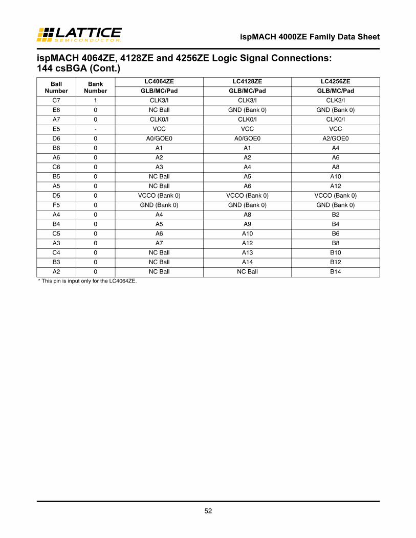
ispMACH 4000ZE Family Data Sheet
52
C7 1 CLK3/I CLK3/I CLK3/I
E6 0 NC Ball GND (Bank 0) GND (Bank 0)
A7 0 CLK0/I CLK0/I CLK0/I
E5 - VCC VCC VCC
D6 0 A0/GOE0 A0/GOE0 A2/GOE0
B6 0 A1 A1 A4
A6 0 A2 A2 A6
C6 0 A3 A4 A8
B5 0 NC Ball A5 A10
A5 0 NC Ball A6 A12
D5 0 VCCO (Bank 0) VCCO (Bank 0) VCCO (Bank 0)
F5 0 GND (Bank 0) GND (Bank 0) GND (Bank 0)
A4 0 A4 A8 B2
B4 0 A5 A9 B4
C5 0 A6 A10 B6
A3 0 A7 A12 B8
C4 0 NC Ball A13 B10
B3 0 NC Ball A14 B12
A2 0 NC Ball NC Ball B14
* This pin is input only for the LC4064ZE.
ispMACH 4064ZE, 4128ZE and 4256ZE Logic Signal Connections: 144 csBGA (Cont.)
BallNumber
BankNumber
LC4064ZE LC4128ZE LC4256ZE
GLB/MC/Pad GLB/MC/Pad GLB/MC/Pad

ispMACH 4000ZE Family Data Sheet
53
ispMACH 4128ZE and 4256ZE Logic Signal Connections: 144 TQFP
Pin Number Bank Number
LC4128ZE LC4256ZE
GLB/MC/Pad GLB/MC/Pad
1 - GND GND
2 - TDI TDI
3 0 VCCO (Bank 0) VCCO (Bank 0)
4 0 B0 C12
5 0 B1 C10
6 0 B2 C8
7 0 B4 C6
8 0 B5 C4
9 0 B6 C2
10 0 GND (Bank 0) GND (Bank 0)
11 0 B8 D14
12 0 B9 D12
13 0 B10 D10
14 0 B12 D8
15 0 B13 D6
16 0 B14 D4
17* 0 NC I
18 0 GND (Bank 0) NC
19 0 VCCO (Bank 0) VCCO (Bank 0)
20* 0 NC I
21 0 C14 E2
22 0 C13 E4
23 0 C12 E6
24 0 C10 E8
25 0 C9 E10
26 0 C8 E12
27 0 GND (Bank 0) GND (Bank 0)
28 0 C6 F2
29 0 C5 F4
30 0 C4 F6
31 0 C2 F8
32 0 C1 F10
33 0 C0 F12
34 0 VCCO (Bank 0) VCCO (Bank 0)
35 - TCK TCK
36 - VCC VCC
37 - GND GND
38* 0 NC I
39 0 D14 G12
40 0 D13 G10
41 0 D12 G8
42 0 D10 G6
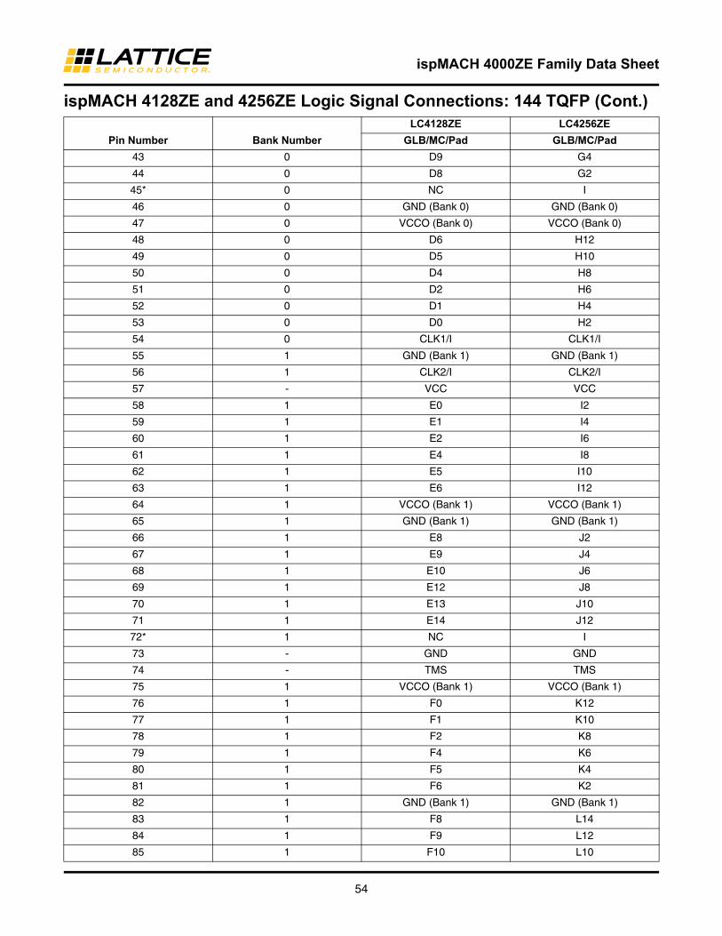
ispMACH 4000ZE Family Data Sheet
54
43 0 D9 G4
44 0 D8 G2
45* 0 NC I
46 0 GND (Bank 0) GND (Bank 0)
47 0 VCCO (Bank 0) VCCO (Bank 0)
48 0 D6 H12
49 0 D5 H10
50 0 D4 H8
51 0 D2 H6
52 0 D1 H4
53 0 D0 H2
54 0 CLK1/I CLK1/I
55 1 GND (Bank 1) GND (Bank 1)
56 1 CLK2/I CLK2/I
57 - VCC VCC
58 1 E0 I2
59 1 E1 I4
60 1 E2 I6
61 1 E4 I8
62 1 E5 I10
63 1 E6 I12
64 1 VCCO (Bank 1) VCCO (Bank 1)
65 1 GND (Bank 1) GND (Bank 1)
66 1 E8 J2
67 1 E9 J4
68 1 E10 J6
69 1 E12 J8
70 1 E13 J10
71 1 E14 J12
72* 1 NC I
73 - GND GND
74 - TMS TMS
75 1 VCCO (Bank 1) VCCO (Bank 1)
76 1 F0 K12
77 1 F1 K10
78 1 F2 K8
79 1 F4 K6
80 1 F5 K4
81 1 F6 K2
82 1 GND (Bank 1) GND (Bank 1)
83 1 F8 L14
84 1 F9 L12
85 1 F10 L10
ispMACH 4128ZE and 4256ZE Logic Signal Connections: 144 TQFP (Cont.)
Pin Number Bank Number
LC4128ZE LC4256ZE
GLB/MC/Pad GLB/MC/Pad
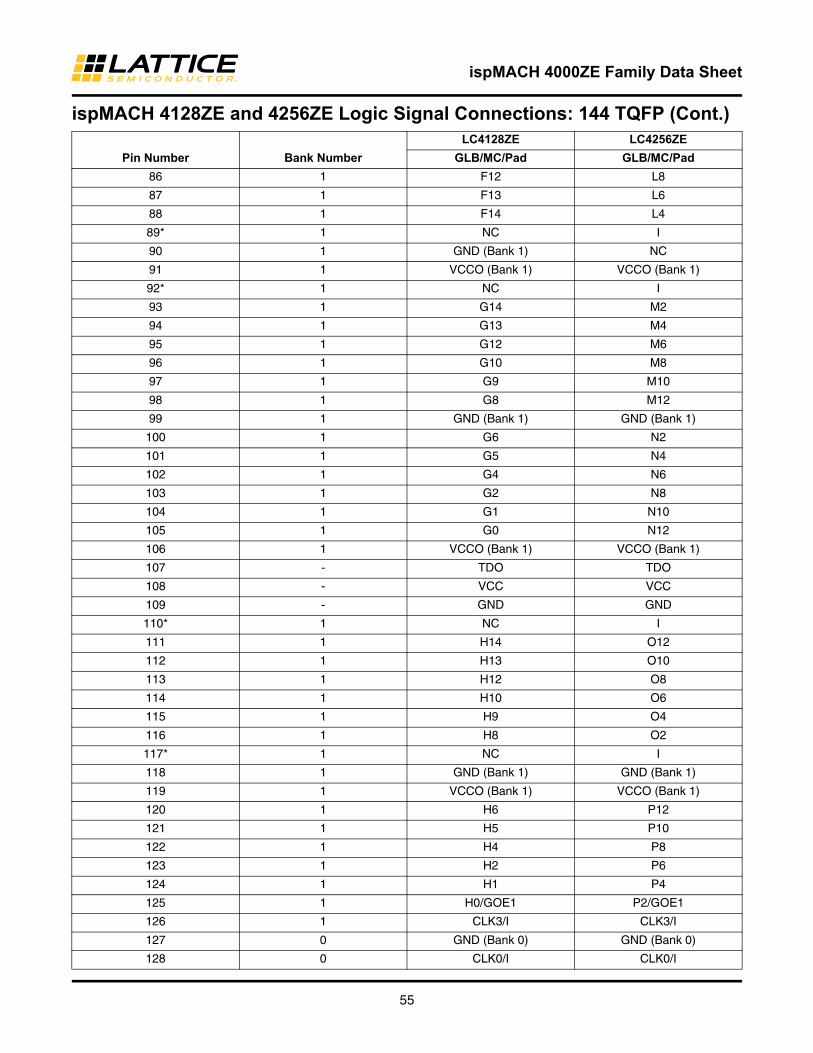
ispMACH 4000ZE Family Data Sheet
55
86 1 F12 L8
87 1 F13 L6
88 1 F14 L4
89* 1 NC I
90 1 GND (Bank 1) NC
91 1 VCCO (Bank 1) VCCO (Bank 1)
92* 1 NC I
93 1 G14 M2
94 1 G13 M4
95 1 G12 M6
96 1 G10 M8
97 1 G9 M10
98 1 G8 M12
99 1 GND (Bank 1) GND (Bank 1)
100 1 G6 N2
101 1 G5 N4
102 1 G4 N6
103 1 G2 N8
104 1 G1 N10
105 1 G0 N12
106 1 VCCO (Bank 1) VCCO (Bank 1)
107 - TDO TDO
108 - VCC VCC
109 - GND GND
110* 1 NC I
111 1 H14 O12
112 1 H13 O10
113 1 H12 O8
114 1 H10 O6
115 1 H9 O4
116 1 H8 O2
117* 1 NC I
118 1 GND (Bank 1) GND (Bank 1)
119 1 VCCO (Bank 1) VCCO (Bank 1)
120 1 H6 P12
121 1 H5 P10
122 1 H4 P8
123 1 H2 P6
124 1 H1 P4
125 1 H0/GOE1 P2/GOE1
126 1 CLK3/I CLK3/I
127 0 GND (Bank 0) GND (Bank 0)
128 0 CLK0/I CLK0/I
ispMACH 4128ZE and 4256ZE Logic Signal Connections: 144 TQFP (Cont.)
Pin Number Bank Number
LC4128ZE LC4256ZE
GLB/MC/Pad GLB/MC/Pad
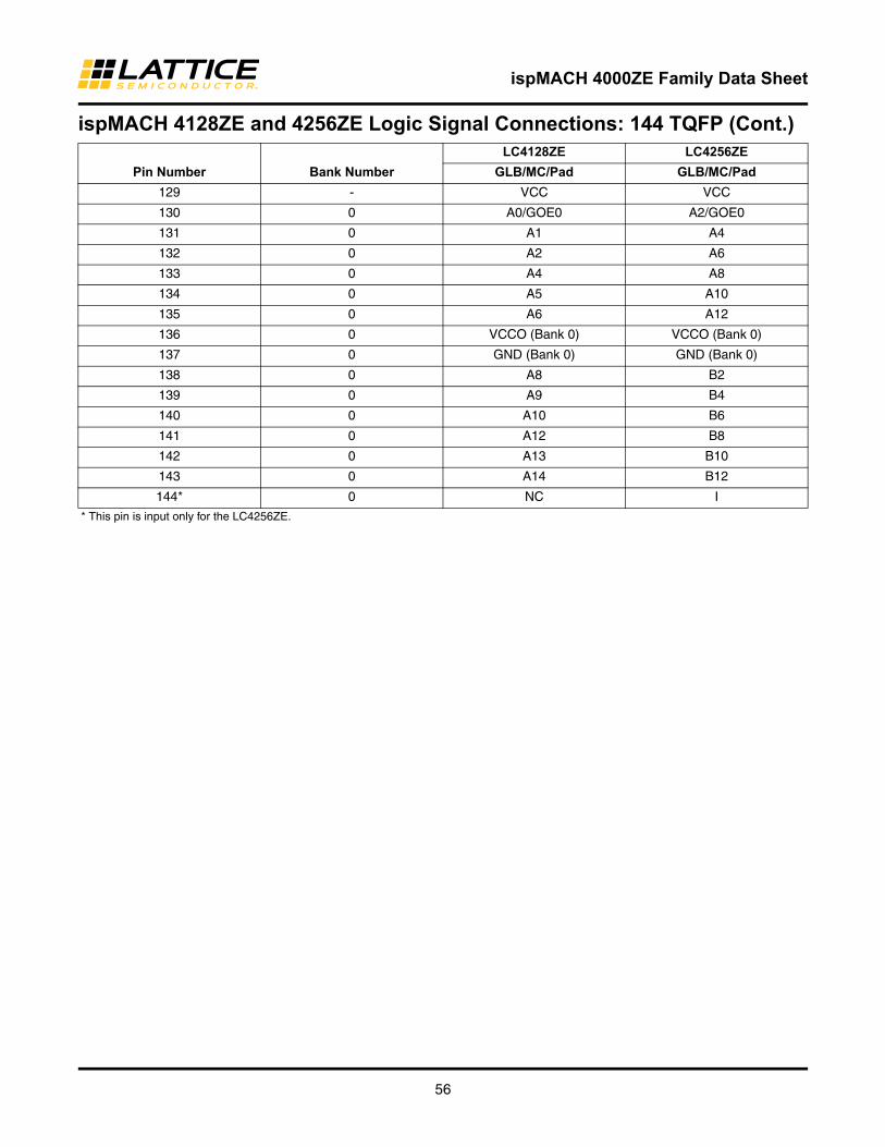
ispMACH 4000ZE Family Data Sheet
56
129 - VCC VCC
130 0 A0/GOE0 A2/GOE0
131 0 A1 A4
132 0 A2 A6
133 0 A4 A8
134 0 A5 A10
135 0 A6 A12
136 0 VCCO (Bank 0) VCCO (Bank 0)
137 0 GND (Bank 0) GND (Bank 0)
138 0 A8 B2
139 0 A9 B4
140 0 A10 B6
141 0 A12 B8
142 0 A13 B10
143 0 A14 B12
144* 0 NC I
* This pin is input only for the LC4256ZE.
ispMACH 4128ZE and 4256ZE Logic Signal Connections: 144 TQFP (Cont.)
Pin Number Bank Number
LC4128ZE LC4256ZE
GLB/MC/Pad GLB/MC/Pad
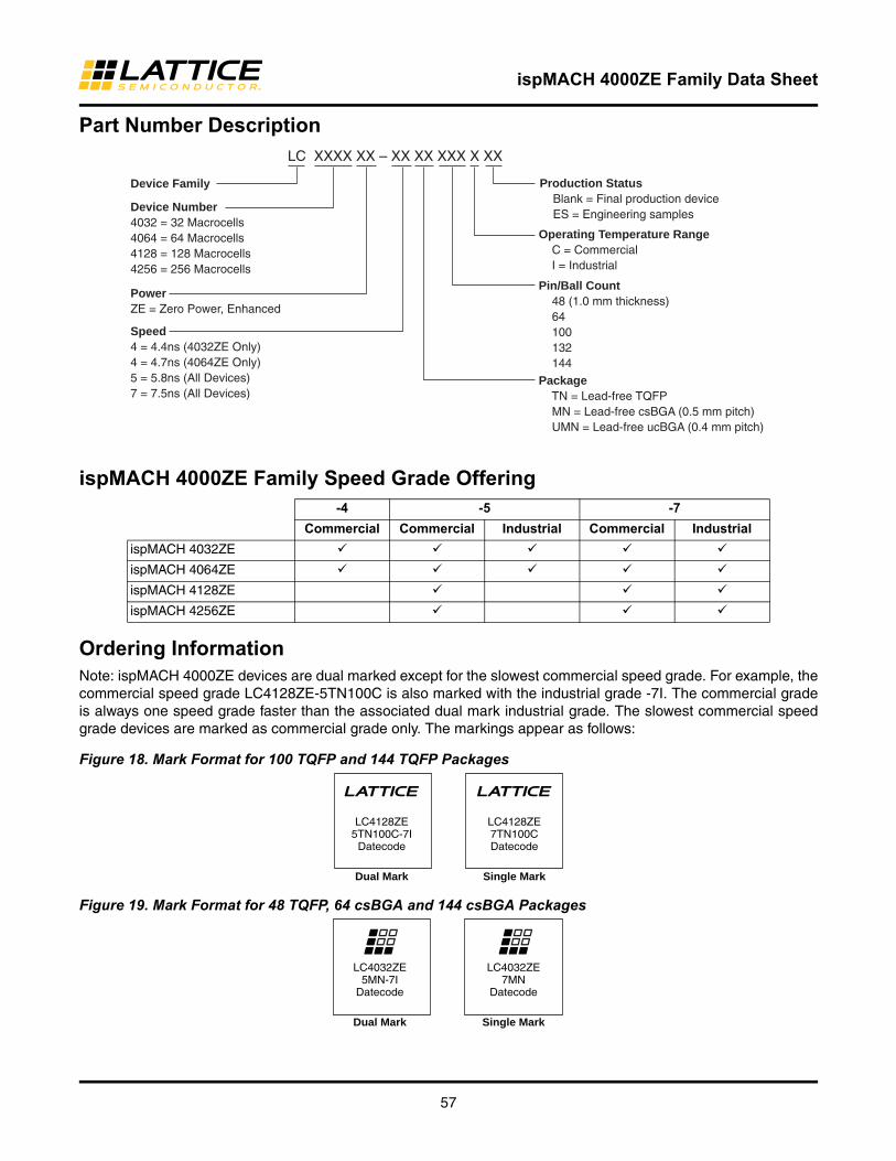
ispMACH 4000ZE Family Data Sheet
57
Part Number Description
ispMACH 4000ZE Family Speed Grade Offering
Ordering InformationNote: ispMACH 4000ZE devices are dual marked except for the slowest commercial speed grade. For example, thecommercial speed grade LC4128ZE-5TN100C is also marked with the industrial grade -7I. The commercial gradeis always one speed grade faster than the associated dual mark industrial grade. The slowest commercial speedgrade devices are marked as commercial grade only. The markings appear as follows:
Figure 18. Mark Format for 100 TQFP and 144 TQFP Packages
Figure 19. Mark Format for 48 TQFP, 64 csBGA and 144 csBGA Packages
-4 -5 -7
Commercial Commercial Industrial Commercial Industrial
ispMACH 4032ZE
ispMACH 4064ZE
ispMACH 4128ZE
ispMACH 4256ZE
Device Number4032 = 32 Macrocells4064 = 64 Macrocells4128 = 128 Macrocells4256 = 256 Macrocells
LC XXXX XX – XX XX XXX X XX
Production Status Blank = Final production device ES = Engineering samples
PowerZE = Zero Power, Enhanced
Speed4 = 4.4ns (4032ZE Only)4 = 4.7ns (4064ZE Only)5 = 5.8ns (All Devices)7 = 7.5ns (All Devices)
Pin/Ball Count 48 (1.0 mm thickness) 64 100 132 144
Package TN = Lead-free TQFP MN = Lead-free csBGA (0.5 mm pitch) UMN = Lead-free ucBGA (0.4 mm pitch)
Operating Temperature Range C = Commercial I = Industrial
Device Family
LC4128ZE5TN100C-7I
Datecode
LC4128ZE7TN100CDatecode
Dual Mark Single Mark
LC4032ZE5MN-7I
Datecode
LC4032ZE7MN
Datecode
Dual Mark Single Mark
ispMACH 4000ZE Family Data Sheet
58
Figure 20. Mark Format for 64 ucBGA and 132 ucBGA Packages
Lead-Free PackagingCommercial
Device Part Number Macrocells Voltage tPD Package Pin/BallCount I/O Grade
LC4032ZE
LC4032ZE-4TN48C 32 1.8 4.4 Lead-Free TQFP 48 32 C
LC4032ZE-5TN48C 32 1.8 5.8 Lead-Free TQFP 48 32 C
LC4032ZE-7TN48C 32 1.8 7.5 Lead-Free TQFP 48 32 C
LC4032ZE-4MN64C 32 1.8 4.4 Lead-Free csBGA 64 32 C
LC4032ZE-5MN64C 32 1.8 5.8 Lead-Free csBGA 64 32 C
LC4032ZE-7MN64C 32 1.8 7.5 Lead-Free csBGA 64 32 C
LC4064ZE
LC4064ZE-4TN48C 64 1.8 4.7 Lead-Free TQFP 48 32 C
LC4064ZE-5TN48C 64 1.8 5.8 Lead-Free TQFP 48 32 C
LC4064ZE-7TN48C 64 1.8 7.5 Lead-Free TQFP 48 32 C
LC4064ZE-4TN100C 64 1.8 4.7 Lead-Free TQFP 100 64 C
LC4064ZE-5TN100C 64 1.8 5.8 Lead-Free TQFP 100 64 C
LC4064ZE-7TN100C 64 1.8 7.5 Lead-Free TQFP 100 64 C
LC4064ZE-4MN64C 64 1.8 4.7 Lead-Free csBGA 64 48 C
LC4064ZE-5MN64C 64 1.8 5.8 Lead-Free csBGA 64 48 C
LC4064ZE-7MN64C 64 1.8 7.5 Lead-Free csBGA 64 48 C
LC4064ZE-4MN144C 64 1.8 4.7 Lead-Free csBGA 144 64 C
LC4064ZE-5MN144C 64 1.8 5.8 Lead-Free csBGA 144 64 C
LC4064ZE-7MN144C 64 1.8 7.5 Lead-Free csBGA 144 64 C
LC4128ZE
LC4128ZE-5TN100C 128 1.8 5.8 Lead-Free TQFP 100 64 C
LC4128ZE-7TN100C 128 1.8 7.5 Lead-Free TQFP 100 64 C
LC4128ZE-5TN144C 128 1.8 5.8 Lead-Free TQFP 144 96 C
LC4128ZE-7TN144C 128 1.8 7.5 Lead-Free TQFP 144 96 C
LC4128ZE-5UMN132C 128 1.8 5.8 Lead-Free ucBGA 132 96 C
LC4128ZE-7UMN132C 128 1.8 7.5 Lead-Free ucBGA 132 96 C
LC4128ZE-5MN144C 128 1.8 5.8 Lead-Free csBGA 144 96 C
LC4128ZE-7MN144C 128 1.8 7.5 Lead-Free csBGA 144 96 C
LC4256ZE
LC4256ZE-5TN100C 256 1.8 5.8 Lead-Free TQFP 100 64 C
LC4256ZE-7TN100C 256 1.8 7.5 Lead-Free TQFP 100 64 C
LC4256ZE-5TN144C 256 1.8 5.8 Lead-Free TQFP 144 96 C
LC4256ZE-7TN144C 256 1.8 7.5 Lead-Free TQFP 144 96 C
LC4256ZE-5MN144C 256 1.8 5.8 Lead-Free csBGA 144 108 C
LC4256ZE-7MN144C 256 1.8 7.5 Lead-Free csBGA 144 108 C
LC4064ZE4UN-5I
Datecode
LC4128ZE7UN
Datecode
Dual Mark Single Mark
ispMACH 4000ZE Family Data Sheet
59
For Further InformationIn addition to this data sheet, the following technical notes may be helpful when designing with the ispMACH4000ZE family:
• TN1168, ispMACH 4000ZE Timing Model Design and Usage Guidelines• TN1174, Advanced Features of the ispMACH 4000ZE Family• TN1187, Power Estimation in ispMACH 4000ZE Devices• Package Diagrams
Technical Support AssistanceHotline: 1-800-LATTICE (North America)
+1-503-268-8001 (Outside North America)e-mail: [email protected]: www.latticesemi.com
Industrial
Device Part Number Macrocells Voltage tPD Package Pin/BallCount I/O Grade
LC4032ZE
LC4032ZE-5TN48I 32 1.8 5.8 Lead-Free TQFP 48 32 I
LC4032ZE-7TN48I 32 1.8 7.5 Lead-Free TQFP 48 32 I
LC4032ZE-5MN64I 32 1.8 5.8 Lead-Free csBGA 64 32 I
LC4032ZE-7MN64I 32 1.8 7.5 Lead-Free csBGA 64 32 I
LC4064ZE
LC4064ZE-5TN48I 64 1.8 5.8 Lead-Free TQFP 48 32 I
LC4064ZE-7TN48I 64 1.8 7.5 Lead-Free TQFP 48 32 I
LC4064ZE-5TN100I 64 1.8 5.8 Lead-Free TQFP 100 64 I
LC4064ZE-7TN100I 64 1.8 7.5 Lead-Free TQFP 100 64 I
LC4064ZE-5MN64I 64 1.8 5.8 Lead-Free csBGA 64 48 I
LC4064ZE-7MN64I 64 1.8 7.5 Lead-Free csBGA 64 48 I
LC4064ZE-5UMN64I 64 1.8 5.8 Lead-Free ucBGA 64 48 I
LC4064ZE-7UMN64I 64 1.8 7.5 Lead-Free ucBGA 64 48 I
LC4064ZE-5MN144I 64 1.8 5.8 Lead-Free csBGA 144 64 I
LC4064ZE-7MN144I 64 1.8 7.5 Lead-Free csBGA 144 64 I
LC4128ZE
LC4128ZE-7TN100I 128 1.8 7.5 Lead-Free TQFP 100 64 I
LC4128ZE-7UMN132I 128 1.8 7.5 Lead-Free ucBGA 132 96 I
LC4128ZE-7TN144I 128 1.8 7.5 Lead-Free TQFP 144 96 I
LC4128ZE-7MN144I 128 1.8 7.5 Lead-Free csBGA 144 96 I
LC4256ZE
LC4256ZE-7TN100I 256 1.8 7.5 Lead-Free TQFP 100 64 I
LC4256ZE-7TN144I 256 1.8 7.5 Lead-Free TQFP 144 96 I
LC4256ZE-7MN144I 256 1.8 7.5 Lead-Free csBGA 144 108 I
1. Contact factory for product availability.
ispMACH 4000ZE Family Data Sheet
60
Revision HistoryDate Version Change Summary
April 2008 01.0 Initial release.
July 2008 01.1 Updated Features bullets.
Updated typical Hysteresis voltage.
Updated Power Guard for Dedicated Inputs section.
Updated DC Electrical Characteristics table.
Updated Supply Current table.
Updated I/O DC Electrical Characteristics table and note 2.
Updated ispMACH 4000ZE Timing Model.
Added new parameters for the Internal Oscillator.
Updated ORP Reference table.
Updated Power Supply and NC Connections table.
Updated 100 TQFP Logic Signal Connections table with LC4128ZE and 4256ZE.
Updated 144 csBGA Logic Signal Connections table with LC4128ZE and 4256ZE.
Added 144 TQFP Logic Signal Connections table.
August 2008 01.2 Data sheet status changed from advance to final.
Updated Supply Current table.
Updated External Switching Characteristics.
Updated Internal Timing Parameters.
Updated Power Consumption graph and Power Estimation Coefficients table.
Updated Ordering Information mark format example.
December 2008 01.3 Updated ispMACH 4000ZE Family Selection Guide table to include 64-ball ucBGA and 132-ball ucBGA packages.
Updated ispMACH 4000ZE Power Supply and NC Connections table to include 64-ball ucBGA and 132-ball ucBGA packages.
Added Logic Signal Connections tables for 64-ball ucBGA and 132-ball ucBGA packages.
Updated Part Number Description diagram for 64-ball ucBGA and 132-ball ucBGA packages.
Updated Ordering Information tables for 64-ball ucBGA and 132-ball ucBGA packages.
May 2009 01.4 Correction to tCW, tGW, tWIR and fMAX parameters in External Switching Characteristics table.
June 2011 01.5 Added copper bond package part numbers.
Added footnote 4 to Absolute Maximum Ratings.
February 2012 01.6 Updated document with new corporate logo.
February 2012 01.7 Removed copper bond packaging information. Refer to PCN 04A-12 for further information.
Updated topside marks with new logos in the Ordering Information section.