Isolation Design Flow for the Zynq UltraScale+ …...Access the isolation design for this...
33
Summary This applicaon note describes how to implement security- or safety-crical designs using the Xilinx ® Isolaon Design Flow (IDF) with the Xilinx Vivado ® Design Suite. Design applicaons include informaon assurance (single-chip cryptography), avionics, automove, and industrial applicaons. This document explains how to: • Implement isolated funcons in a Xilinx UltraScale+™ device or a Zynq ® UltraScale+™ MPSoC • Verify the isolaon using the Xilinx Vivado Isolaon Verifier (VIV) To add addional security to your design, purchase the Security Monitor IP developed by Xilinx. If you embed this IP, modificaons to the steps in this document must be made. For more informaon, see Integraon and Verificaon of Security Monitor 3.0 for Zynq UltraScale. Also refer to the Aerospace and Defense Security Monitor IP Core Product Markeng Brief. Contact your local Xilinx ® representave for more informaon and access to these documents. If the target applicaon requires mask control, a defense-grade (XQ) device might be needed. This applicaon note specifically covers UltraScale+ devices and Zynq UltraScale+ MPSoC devices using Vivado Design Suite 2018.3, and builds on earlier IDF concepts. An example design is provided in the Isolaon Design Example for Zynq Ultrascale+ MPSoC Applicaon Note (XAPP1336). For more informaon see Isolaon Design Example. Introduction The flexibility of programmable logic affords security-crical and safety-crical industries many advantages. However, before Isolaon Design Flow (IDF) was developed, in applicaons, such as informaon assurance, government contractors and agencies could not realize the full capability of programmable logic due to isolaon, reliability, and security concerns, and were therefore forced to use mulchip soluons. To address these concerns, the IDF was developed to allow independent funcons to operate on a single chip. Examples of single chip applicaons include, but are not limited to, redundant Type- I cryptographic modules, or resident safety- and non safety-crical funcons. The successful compleon of the Xilinx ® Isolaon Design Flow allows Xilinx to provide new technology for the informaon assurance (IA) industry, as well as, provide safety-crical funcons in avionics, automove, and industrial applicaons. Application Note: UltraScale+ Devices, Zynq UltraScale+ MPSoC Isolation Design Flow for UltraScale+ Devices and the Zynq UltraScale+ MPSoC XAPP1335 (v1.1) April 15, 2019 XAPP1335 (v1.1) April 15, 2019 www.xilinx.com Application Note 1
Transcript of Isolation Design Flow for the Zynq UltraScale+ …...Access the isolation design for this...

SummaryThis application note describes how to implement security- or safety-critical designs using theXilinx® Isolation Design Flow (IDF) with the Xilinx Vivado® Design Suite. Design applicationsinclude information assurance (single-chip cryptography), avionics, automotive, and industrialapplications. This document explains how to:
• Implement isolated functions in a Xilinx UltraScale+™ device or a Zynq® UltraScale+™ MPSoC
• Verify the isolation using the Xilinx Vivado Isolation Verifier (VIV)
To add additional security to your design, purchase the Security Monitor IP developed by Xilinx.If you embed this IP, modifications to the steps in this document must be made. For moreinformation, see Integration and Verification of Security Monitor 3.0 for Zynq UltraScale. Also referto the Aerospace and Defense Security Monitor IP Core Product Marketing Brief. Contact yourlocal Xilinx® representative for more information and access to these documents. If the targetapplication requires mask control, a defense-grade (XQ) device might be needed.
This application note specifically covers UltraScale+ devices and Zynq UltraScale+ MPSoCdevices using Vivado Design Suite 2018.3, and builds on earlier IDF concepts.
An example design is provided in the Isolation Design Example for Zynq Ultrascale+ MPSoCApplication Note (XAPP1336). For more information see Isolation Design Example.
IntroductionThe flexibility of programmable logic affords security-critical and safety-critical industries manyadvantages. However, before Isolation Design Flow (IDF) was developed, in applications, such asinformation assurance, government contractors and agencies could not realize the full capabilityof programmable logic due to isolation, reliability, and security concerns, and were thereforeforced to use multichip solutions.
To address these concerns, the IDF was developed to allow independent functions to operate ona single chip. Examples of single chip applications include, but are not limited to, redundant Type-I cryptographic modules, or resident safety- and non safety-critical functions.
The successful completion of the Xilinx® Isolation Design Flow allows Xilinx to provide newtechnology for the information assurance (IA) industry, as well as, provide safety-criticalfunctions in avionics, automotive, and industrial applications.
Application Note: UltraScale+ Devices, Zynq UltraScale+ MPSoC
Isolation Design Flow forUltraScale+ Devices and the
Zynq UltraScale+ MPSoCXAPP1335 (v1.1) April 15, 2019
XAPP1335 (v1.1) April 15, 2019 www.xilinx.comApplication Note 1

Isolation Design Flow OverviewDeveloping a safe and secure single chip solution containing multiple isolated functions in asingle FPGA is made possible through Xilinx® isolation technology. Special attributes, such asHD.ISOLATED and the features it enables, are necessary to provide controls to achieve theisolation needed to meet certifying agency requirements.
To better understand the details of the Isolation Design Flow (IDF), the designer should have asolid understanding of the hierarchical design flow (see Hierarchical Design User Guide (UG905).Many of the terms and processes in the partition flow are used in the IDF. Areas that aredifferent supersede the partition design flow and are identified in this application note.
Common TerminologyThroughout this document, the terms ownership, function, logic, region, and fence are usedextensively. These terms are defined as follows:
• Ownership (physical/logical): The concept of physical versus logical ownership is an importantconcept to understand when using the IDF. This concept is described below under "TrustedRouting".
• Function: A collection of logic that performs a specific operation (for example, an AESencryptor).
• Logic: Circuits used to implement a specific function (for example, flip-flop, look up table, andRAM).
• Isolated Region/Pblock: A physical area to place logic.
• Fence: The concept of physical versus logical ownership is an important concept comprised ofa set of unused tiles in which no routine or logic is present.
• Trusted Routing: The routes that satisfy the rules outlined in the following figures. Trustedrouting is automatically enabled after the HD.ISOLATED attribute is set to TRUE on at leastone isolated module. These routes are a subset of existing routing resources that meet thefollowing restrictions:
• No entry or exit point in the fence between isolated regions
• One source and one destination region
• Its entirety stays contained in the source/destination regions
• It does not come within one fence tile from another unintended isolation region
These rules act as a filter to all available routes in a given design. An example of routes thatwould be filtered are shown in the following figures. Example routes excluded forprogrammable interconnect points (PIPs) outside the intended isolation regions or proximity tounintended isolation regions are also shown.
Isolation Design Flow for UltraScale+ Devices and the Zynq UltraScale+MPSoC
XAPP1335 (v1.1) April 15, 2019 www.xilinx.comApplication Note 2

Figure 1: Trusted Routes within an Isolated Module
Figure 2: Trusted Routes between Isolated Modules
RulesA secure or safety-critical solution can be achieved while using FPGA design techniques andcoding styles with only moderate modifications to the development flow. Xilinx® Isolation DesignFlow (IDF) development requires the designer to consider floorplanning much earlier in thedesign process to ensure that proper isolation is achieved in logic, routing, and I/O buffers (IOBs).In addition to early floorplanning, the development flow is based on hierarchy. That is, eachfunction you wish to isolate must be at its own level of hierarchy. Although this flow requiresadditional steps, the hierarchical approach has certain advantages.
There are a few unique design details that must be adhered to achieve an FPGA-based IDFsolution. Carefully consider all aspects of the design details explained in subsequent sections ofthis application note. These considerations include:
• Each function to be isolated must be in its own level of hierarchy.
• A fence must be used to separate isolated functions.
Isolation Design Flow for UltraScale+ Devices and the Zynq UltraScale+MPSoC
XAPP1335 (v1.1) April 15, 2019 www.xilinx.comApplication Note 3

• IOBs must be instantiated inside isolated modules for proper isolation of the IOB. This can beachieved by manual user instantiation or automatically by the tools.
Note: Automatic logical inferencing by the tools is unique to the Vivado® Design Suite.
• On-chip communication between isolated functions is achieved through the use of trustedrouting (Tools automatically choose trusted routes along coincident physical borders).
Top Level LogicIsolated designs must keep the amount of top level logic to a minimum. In a typical IsolationDesign Flow (IDF) design, the only logic at the top level should be clock logic. Any componentthat is not part of an isolated module in the design hierarchy is optimized to the top level.Because isolation is defined by the HD.ISOLATED attribute being set on a hierarchical module, alltop logic is, by default, not isolated. This has the following implications:
• There are no placement constraints on top level logic other than it will not be placed in thefence.
• Top level logic can be placed in any isolated region.
• There are no routing restrictions on top level logic other than it will not violate the fence withused programmable interconnect points (PIPs).
• Top level routes can route to, from, and through any isolated region.
Reference DesignFor clarity, an example single-chip 2 channel functional safety design is used throughout thisapplication note to describe the design details and tool flow. The following figure shows thefloorplan for the lab design as implemented in an XCZU5CG-SFVC784-1-e device. It consists offive isolated regions. In addition, this design has been implemented with Vivado® Design Suite2018.3, verified by the Vivado Isolation Verifier (VIV) 2.0, and provided to the designer as areference.
Figure 3: IDF Design Floorplan
Isolation Design Flow for UltraScale+ Devices and the Zynq UltraScale+MPSoC
XAPP1335 (v1.1) April 15, 2019 www.xilinx.comApplication Note 4

Access the isolation design for this application note and the Isolation Design Example for ZynqUltrascale+ MPSoC Application Note (XAPP1336) from the Functional Safety lounge.
Architecture OverviewMPSoC Chip LayoutXilinx® MPSoC devices are made up of several sections connected to each other. The processorsystem (PS) is a monolithic block which is connected to the programmable logic (PL) through a setof interconnect tiles. The PS is made up of columns of tiles organized into clock regions as shownin the following figure for the ZU5 architecture.
Figure 4: ZU5 Layout
Clock Regions and ColumnsEach MPSoC is built using similar architecture. The ZU5 programmable logic (PL) uses four rowsof three clock regions. Each clock region contains multiple columns of PL and dedicated block.Each column is composed of a single type of tiles. The number of tiles per column depends onthe height of the tile type. A column of configurable logic block (CLB) tiles has 60 tiles.
The PCIe® tile is an example of the the highest tile used. A column of PCIe has one tile. Thecolumn width changes based on the tile type for that tile.
It is important to understand that the column width for clock regions vertically arranged isconstant. In other words, a column of CLB tiles in the blue clock region extends to the samecolumn in the red clock region below it all the way to the last clock region going vertically downso the same width of the column is maintained from clock region to clock region.
Isolation Design Flow for UltraScale+ Devices and the Zynq UltraScale+MPSoC
XAPP1335 (v1.1) April 15, 2019 www.xilinx.comApplication Note 5

Clock Spines and Interconnect ColumnsThe clock spine for each clock region is located in the center of each clock region as shown in thefollowing figure. The clocks are distributed vertically using the columns of interconnect tileswhich then drive local logic devices in other tiles.
Figure 5: Clock Spine Location
Interconnect tiles are used to route connections between logic tiles. These interconnect tiles arethe equivalent to route channels in ASIC designs, and also provide a convenient method toisolate logic regions.
Pblocks and Programmable UnitsA Pblock is a region made up of logic blocks called programmable units (PUs). Pblock are used todefine an isolated logical unit.
A PU is the smallest logic building block that can be assigned to a Pblock. A Pblock is created byselecting multiple PUs, which create large regions of logic.
Programmable Unit SizesIt is important to include enough required programmable unit (PU) resources in a Pblock tosupport the assigned hierarchy. This is verified by reviewing the resources table when the Pblockis drawn.
Each PU has a height, defined by how many PUs can fit in a clock region column, and a widthdefined by how many columns are needed to support the PU function. A Pblock can be anyshape. The shape is defined by the combination if PUs are selected.
Table 1: PU Unit Sizes
Programmable Unit (PU) User Tile Description Fence SizeSLICEL (CLBL) Configurable Logic Block. The key logic
unit of an FPGA.Vertical: 1 PUHorizontal: 1 PU
SLICEM (CLBM) Configurable Logic Block. The key logicunit of an FPGA.
Vertical: 1 PUHorizontal: 1 PU
DSP Digital Signal Processor. Aprogrammable math function (DSP tileis two DSP48E1 slices; analysis wasdone on DSP48E1 slice; Vivado® toolsonly allow selection of a DSP tile).
Vertical: 1 PUHorizontal: 1 PU
Isolation Design Flow for UltraScale+ Devices and the Zynq UltraScale+MPSoC
XAPP1335 (v1.1) April 15, 2019 www.xilinx.comApplication Note 6
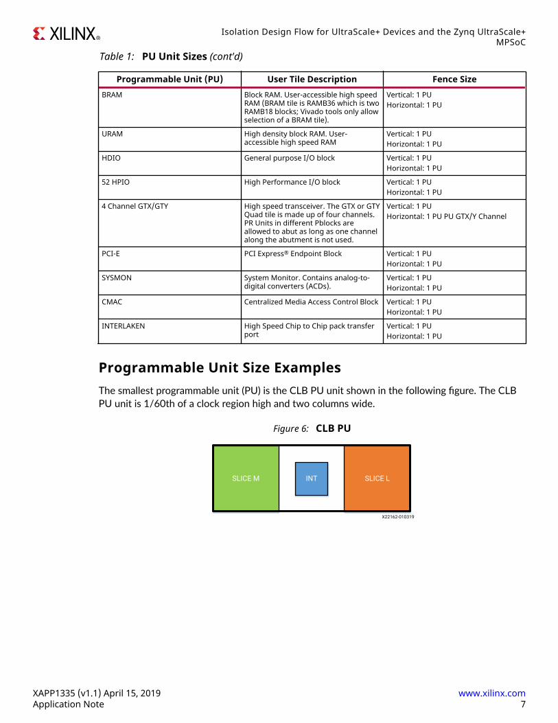
Table 1: PU Unit Sizes (cont'd)
Programmable Unit (PU) User Tile Description Fence SizeBRAM Block RAM. User-accessible high speed
RAM (BRAM tile is RAMB36 which is twoRAMB18 blocks; Vivado tools only allowselection of a BRAM tile).
Vertical: 1 PUHorizontal: 1 PU
URAM High density block RAM. User-accessible high speed RAM
Vertical: 1 PUHorizontal: 1 PU
HDIO General purpose I/O block Vertical: 1 PUHorizontal: 1 PU
52 HPIO High Performance I/O block Vertical: 1 PUHorizontal: 1 PU
4 Channel GTX/GTY High speed transceiver. The GTX or GTYQuad tile is made up of four channels.PR Units in different Pblocks areallowed to abut as long as one channelalong the abutment is not used.
Vertical: 1 PUHorizontal: 1 PU PU GTX/Y Channel
PCI-E PCI Express® Endpoint Block Vertical: 1 PUHorizontal: 1 PU
SYSMON System Monitor. Contains analog-to-digital converters (ACDs).
Vertical: 1 PUHorizontal: 1 PU
CMAC Centralized Media Access Control Block Vertical: 1 PUHorizontal: 1 PU
INTERLAKEN High Speed Chip to Chip pack transferport
Vertical: 1 PUHorizontal: 1 PU
Programmable Unit Size ExamplesThe smallest programmable unit (PU) is the CLB PU unit shown in the following figure. The CLBPU unit is 1/60th of a clock region high and two columns wide.
Figure 6: CLB PU
SLICE M INT SLICE L
X22162-010319
Isolation Design Flow for UltraScale+ Devices and the Zynq UltraScale+MPSoC
XAPP1335 (v1.1) April 15, 2019 www.xilinx.comApplication Note 7
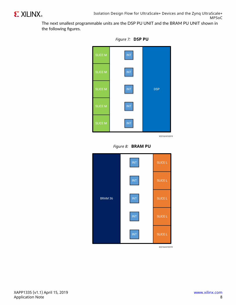
The next smallest programmable units are the DSP PU UNIT and the BRAM PU UNIT shown inthe following figures.
Figure 7: DSP PU
SLICE M INT
DSP
INTSLICE M
SLICE M
SLICE M
SLICE M
INT
INT
INT
X22163-010319
Figure 8: BRAM PU
BRAM 36
SLICE LINT
INT
INT
INT
INT
SLICE L
SLICE L
SLICE L
SLICE L
X22164-010319
Isolation Design Flow for UltraScale+ Devices and the Zynq UltraScale+MPSoC
XAPP1335 (v1.1) April 15, 2019 www.xilinx.comApplication Note 8

The URAM PU shown in the following figure.
Figure 9: URAM PU
SLICE M
URAM
SLICE LINT
INT
INT
INT
INT
INT
INT
INT
INT
INT
INT
INT
INT
INT
INT
INT
INT
INT
INT
INT
INT
INT
INT
INT
INT
INT
INT
INT
INT
INT
SLICE M SLICE L
SLICE M
SLICE M
SLICE M
SLICE L
SLICE L
SLICE L
SLICE M
SLICE M
SLICE M
SLICE M
SLICE M
SLICE M
SLICE M
SLICE M
SLICE M
SLICE M
SLICE L
SLICE L
SLICE L
SLICE L
SLICE L
SLICE L
SLICE L
SLICE L
SLICE L
SLICE L
X22165-010319
The highest PUs are:
• 52 HPIO PU: One clock region high and two columns wide
• 4 Channel GTH PU: One clock region high and three columns wide
• SYSMON PU: One clock region high and also three columns wide
Other one clock high PU units include PCIe® and CMAC.
Isolation Design Flow for UltraScale+ Devices and the Zynq UltraScale+MPSoC
XAPP1335 (v1.1) April 15, 2019 www.xilinx.comApplication Note 9

Figure 10: 52 HPIO PU
52 HPIO
INTSLICE L
INTSLICE L
INTSLICE L
SLICE L
SLICE LINT
INT
INTSLICE L
INTSLICE L
INTSLICE L
SLICE L
SLICE LINT
INT
INTSLICE L
INTSLICE L
INTSLICE L
SLICE L
SLICE LINT
INT
INTSLICE L
INTSLICE L
INTSLICE L
SLICE L
SLICE LINT
INT
INTSLICE L
INTSLICE L
INTSLICE L
SLICE L
SLICE LINT
INT
INTSLICE L
INTSLICE L
INTSLICE L
SLICE L
SLICE LINT
INT
INTSLICE L
INTSLICE L
INTSLICE L
SLICE L
SLICE LINT
INT
INTSLICE L
INT SLICE L
INT SLICE L
SLICE L
SLICE L
INT
INT
INT SLICE L
INT SLICE L
INT SLICE L
SLICE L
SLICE L
INT
INT
INT SLICE L
INT SLICE L
INT SLICE L
SLICE L
SLICE L
INT
INT
INT SLICE L
INT SLICE L
INT SLICE L
SLICE L
SLICE L
INT
INT
INT SLICE L
INT SLICE L
INT SLICE L
SLICE L
SLICE L
INT
INT
X22167-010319
Isolation Design Flow for UltraScale+ Devices and the Zynq UltraScale+MPSoC
XAPP1335 (v1.1) April 15, 2019 www.xilinx.comApplication Note 10

Figure 11: 4 Channel GTH PU
INT
4 CHANNEL GTH
SLICE L
SLICE L
SLICE L
SLICE L
SLICE L
SLICE L
SLICE L
SLICE L
SLICE L
SLICE L
INT
SLICE L
SLICE L
SLICE L
SLICE L
SLICE L
SLICE L
SLICE L
SLICE L
SLICE L
SLICE L
SLICE L
SLICE L
SLICE L
SLICE L
SLICE L
SLICE L
SLICE L
SLICE L
SLICE L
SLICE L
SLICE L
SLICE L
SLICE L
SLICE L
SLICE L
SLICE L
SLICE L
SLICE L
SLICE L
SLICE L
SLICE L
SLICE L
SLICE L
SLICE L
SLICE L
SLICE L
SLICE L
SLICE L
SLICE L
SLICE L
SLICE L
SLICE L
SLICE L
SLICE L
SLICE L
SLICE L
SLICE L
SLICE L
SLICE L
SLICE L
INT
INT
INT
INT
INT
INT
INT
INT
INT
INT
INT
INT
INT
INT
INT
INT
INT
INT
INT
INT
INT
INT
INT
INT
INT
INT
INT
INT
INT
INT
INT
INT
INT
INT
INT
INT
INT
INT
INT
INT
INT
INT
INT
INT
INT
INT
INT
INT
INT
INT
INT
INT
INT
INT
INT
INT
INT
INT
X22168-010319
Isolation Design Flow for UltraScale+ Devices and the Zynq UltraScale+MPSoC
XAPP1335 (v1.1) April 15, 2019 www.xilinx.comApplication Note 11

Figure 12: SYSMON PU
SLICE MINT
SYSMON
INTSLICE L
SLICE MSLICE MSLICE MSLICE M
SLICE LSLICE LSLICE LSLICE L
INTINTINTINT
INTINTINTINT
SLICE MINT INT
SLICE LSLICE MSLICE MSLICE MSLICE M
SLICE LSLICE LSLICE LSLICE L
INTINTINTINT
INTINTINTINT
SLICE MINT INT
SLICE LSLICE MSLICE MSLICE MSLICE M
SLICE LSLICE LSLICE LSLICE L
INTINTINTINT
INTINTINTINT
SLICE MINT INT
SLICE LSLICE MSLICE MSLICE MSLICE M
SLICE LSLICE LSLICE LSLICE L
INTINTINTINT
INTINTINTINT
SLICE MINT INT
SLICE LSLICE MSLICE MSLICE MSLICE M
SLICE LSLICE LSLICE LSLICE L
INTINTINTINT
INTINTINTINT
SLICE MINT INT
SLICE LSLICE MSLICE MSLICE MSLICE M
SLICE LSLICE LSLICE LSLICE L
INTINTINTINT
INTINTINTINT
SLICE MINT INT
SLICE LSLICE MSLICE MSLICE MSLICE M
SLICE LSLICE LSLICE LSLICE L
INTINTINTINT
INTINTINTINT
SLICE MINT INT
SLICE LSLICE MSLICE MSLICE MSLICE M
SLICE LSLICE LSLICE LSLICE L
INTINTINTINT
INTINTINTINT
SLICE MINT INT
SLICE LSLICE MSLICE MSLICE MSLICE M
SLICE LSLICE LSLICE LSLICE L
INTINTINTINT
INTINTINTINT
SLICE MINT INT
SLICE LSLICE MSLICE MSLICE MSLICE M
SLICE LSLICE LSLICE LSLICE L
INTINTINTINT
INTINTINTINT
SLICE MINT INT
SLICE LSLICE MSLICE MSLICE MSLICE M
SLICE LSLICE LSLICE LSLICE L
INTINTINTINT
INTINTINTINT
SLICE MINT INT
SLICE LSLICE MSLICE MSLICE MSLICE M
SLICE LSLICE LSLICE LSLICE L
INTINTINTINT
INTINTINTINT
X22169-010319
Isolation Design Flow for UltraScale+ Devices and the Zynq UltraScale+MPSoC
XAPP1335 (v1.1) April 15, 2019 www.xilinx.comApplication Note 12

Figure 13: HDIO PU
SLICE MINT
HDIO
INTSLICE L
SLICE M
SLICE M
SLICE M
SLICE M
SLICE L
SLICE L
SLICE L
SLICE L
INT
INT
INT
INT
INT
INT
INT
INT
SLICE MINT INT
SLICE L
SLICE M
SLICE M
SLICE M
SLICE M
SLICE L
SLICE L
SLICE L
SLICE L
INT
INT
INT
INT
INT
INT
INT
INT
SLICE MINT INT
SLICE L
SLICE M
SLICE M
SLICE M
SLICE M
SLICE L
SLICE L
SLICE L
SLICE L
INT
INT
INT
INT
INT
INT
INT
INT
SLICE MINT INT
SLICE L
SLICE M
SLICE M
SLICE M
SLICE M
SLICE L
SLICE L
SLICE L
SLICE L
INT
INT
INT
INT
INT
INT
INT
INT
SLICE MINT INT
SLICE L
SLICE M
SLICE M
SLICE M
SLICE M
SLICE L
SLICE L
SLICE L
SLICE L
INT
INT
INT
INT
INT
INT
INT
INT
SLICE MINT INT
SLICE L
SLICE M
SLICE M
SLICE M
SLICE M
SLICE L
SLICE L
SLICE L
SLICE L
INT
INT
INT
INT
INT
INT
INT
INT
X22166-010319
Isolation Design Flow for UltraScale+ Devices and the Zynq UltraScale+MPSoC
XAPP1335 (v1.1) April 15, 2019 www.xilinx.comApplication Note 13

FencesA fence is defined as a continuous line of unprogrammed logical resources (unprogrammed usertiles) between a Pblock. These resources also use programmable units (PUs). The fence, like aPblock, can be any shape shown as the translucent area as shown in the following figure. Thefence is formed by drawing Pblocks that are separated by at least one PU. Except for GTprogrammable units, any Pblock that abut to another Pblock will create a fence violation. WhenGT PUs abut, one I/O channel from either GT PU cannot be used at the abutment edge. This un-used I/O channel becomes part of the fence.
A fence width or height needs to be only one PU high or wide. Routing resources across thefence become more limited if the fence is wider that one PU.
Referring to the following figure, two Pblocks are defined (each outlined in purple and red). Thetranslucent tiles are fence.
Figure 14: Pblocks and Fences
Isolation Design Flow for UltraScale+ Devices and the Zynq UltraScale+MPSoC
XAPP1335 (v1.1) April 15, 2019 www.xilinx.comApplication Note 14

Design ProcessThe following figure shows the recommended process for a design using the Isolation DesignFlow (IDF). These steps are key to achieve single-fault hardware isolation required in InformationAssurance and Functional Safety designs.
Figure 15: Design Flow Chart for IDF
IP IntegratorThe IP integrator is where the design is captured in the Vivado® Design Suite. After the design iscaptured, a functional hierarchy is established based on your isolation strategy with respect tohow data is flowing in your design. These create the logical boundaries which will define thephysical isolation as the design flow is implemented. This step is critical as all other activities arebased on this hierarchy.
After the hierarchy is established, an additional wrapper is required. This additional wrapper isrequired to enable port splitting that might not be allowed by tool generated items, such as thehierarchy created by the triple modular redundancy (TMR) management tool (see MicroBlazeTriple Modular Redundancy (TMR) Subsystem Product Guide (PG268).
Isolation Design Flow for UltraScale+ Devices and the Zynq UltraScale+MPSoC
XAPP1335 (v1.1) April 15, 2019 www.xilinx.comApplication Note 15

Figure 16: IP Integrator Tool Generated Design Example
Figure 17: MicroBlaze™ Hierarchy for TMR Manager
Figure 18: MB_SYSTEM Hierarchy
Isolation Design Flow for UltraScale+ Devices and the Zynq UltraScale+MPSoC
XAPP1335 (v1.1) April 15, 2019 www.xilinx.comApplication Note 16

Figure 19: MicroBlaze TMR Completed Automation
Figure 20: Updated MB_SYSTEM Hiearchy with TMR Implemented
Figure 21: MB_SYSTEM Hierarchy Removed to Flatten Design for Wrappers
Isolation Design Flow for UltraScale+ Devices and the Zynq UltraScale+MPSoC
XAPP1335 (v1.1) April 15, 2019 www.xilinx.comApplication Note 17

Figure 22: 5 User-Created Hierarchy (Wrappers)
SimulationThis step is used to verify your functional expectation of your design. No additional actions arerequired to comply with the isolation design flow (IDF).
ElaborationIn Isolation Design Flow (IDF), the HD.ISOLATED property is added and enabled for each user-created wrappers that need to be isolated from each other. All other hierarchies that do notrequire isolation do not get this property added. Such hierarchies will get optimized to top leveland have no place and route restrictions beyond keeping fence intact. At this point in the designflow, this property is added on each wrapper, so synthesis knows which hierarchy is isolated,preventing optimization across isolation boundaries.
Isolation Design Flow for UltraScale+ Devices and the Zynq UltraScale+MPSoC
XAPP1335 (v1.1) April 15, 2019 www.xilinx.comApplication Note 18

Figure 23: Adding Property HD.ISOLATED
Isolation Design Flow for UltraScale+ Devices and the Zynq UltraScale+MPSoC
XAPP1335 (v1.1) April 15, 2019 www.xilinx.comApplication Note 19

Figure 24: Enabling HD.ISOLATED
SynthesisThis step creates the actual logic that is used to implement your design. Before an isolated designcan be implemented, a floorplanning strategy must be manually entered. This placementrestriction uses Pblocks, which are drawn on the device in the Device window. For logic that isoutside an isolated hierarchy (such as top level logic), this logic can be in any Pblock.
Isolation Design Flow for UltraScale+ Devices and the Zynq UltraScale+MPSoC
XAPP1335 (v1.1) April 15, 2019 www.xilinx.comApplication Note 20

FloorplanningFPGA arrays are made up of multiple clock regions with columns of logic resources within eachclock region. Each logic resource has a fixed height which are stacked one on top of another tomake up a column as shown in the following figure. Pblocks span these regions, but if a resource,such as a PCI™ block, which takes an entire clock region, is not enclosed by a single Pblock, it willnot be included in the Pblock. Before creating each Pblock, map out where each Pblock will belocated.
Figure 25: FPGA Layout
Isolation Design Flow for UltraScale+ Devices and the Zynq UltraScale+MPSoC
XAPP1335 (v1.1) April 15, 2019 www.xilinx.comApplication Note 21
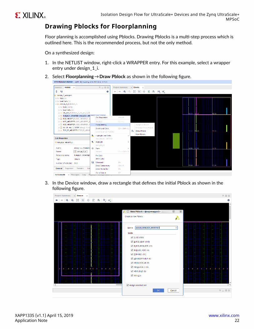
Drawing Pblocks for FloorplanningFloor planning is accomplished using Pblocks. Drawing Pblocks is a multi-step process which isoutlined here. This is the recommended process, but not the only method.
On a synthesized design:
1. In the NETLIST window, right-click a WRAPPER entry. For this example, select a wrapperentry under design_1_i.
2. Select Floorplanning → Draw Pblock as shown in the following figure.
3. In the Device window, draw a rectangle that defines the initial Pblock as shown in thefollowing figure.
Isolation Design Flow for UltraScale+ Devices and the Zynq UltraScale+MPSoC
XAPP1335 (v1.1) April 15, 2019 www.xilinx.comApplication Note 22

Once a Pblock is created, the Statistics Window in Pblock Properties is updated, whichoutlines the percentage the Pblock resources that satisfies the synthesized requirements ofthe isolated region hierarchy as shown in the following figure.
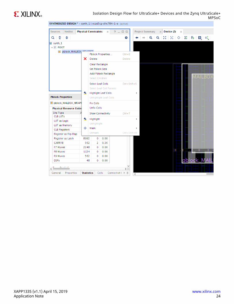
4. To add more resources to a Pblock, in the Device window, select the Pblock to highlight theregion.
5. Right-click the highlighted region, and select Add Pblock Rectangle. As you grow the size ofthe Pblock, the Statistics window will update showing added resources. Pblocks can be anyshape.
6. To delete the Pblock completely, in the Window drop down menu under Physical Constraints,right-click the Pblock entry, and click Delete as shown in the following figure.
Isolation Design Flow for UltraScale+ Devices and the Zynq UltraScale+MPSoC
XAPP1335 (v1.1) April 15, 2019 www.xilinx.comApplication Note 23
Isolation Design Flow for UltraScale+ Devices and the Zynq UltraScale+MPSoC
XAPP1335 (v1.1) April 15, 2019 www.xilinx.comApplication Note 24

When drawing Pblocks, you will see shaded resources that show you which resources areincluded in the Pblock and which are not. All resources not in a Pblock (non-shaded) arefences. In the following figure, the red shaded resources are allocated to one Pblock, thegreen shaded resources are allocated to a second Pblock, and the blue shaded resources areallocated to a third Pblock. The regions outlines are only guidance artifacts from creating thePblock and do not define resources. All non-shaded resources are fences, which means thoseresources are not be used.
Isolation Design Flow for UltraScale+ Devices and the Zynq UltraScale+MPSoC
XAPP1335 (v1.1) April 15, 2019 www.xilinx.comApplication Note 25

Pblocks can be any shape and size as shown in the following figure. This design enablesgreen, red, and blue Pblocks to easily route to each other. The orange Pblock has all of thetop level logic, and the yellow Pblock routes the orange Pblock.
7. To complete the design and make sure your Pblock includes the required I/O Bank, assignpins. In this example, the orange Pblock is top level that also contains the design I/Os.
In the Window drop down menu, select IO Ports to display the I/O Ports window.
Note: In the following figure, the target I/O block is part of the orange Pblock, which is assigned to the toplevel logic. Make sure each Pin Assignment is fixed and has the correct I/O standard; otherwise, the finaldesign rule check (DRCs) ran under Generate Bitstream will fail.
Isolation Design Flow for UltraScale+ Devices and the Zynq UltraScale+MPSoC
XAPP1335 (v1.1) April 15, 2019 www.xilinx.comApplication Note 26

Vivado IDF Verifier (VIV) Checks 1,2,3, and 4In Vivado® Design Suite 2018.3 and later versions, Vivado Isolation Design Verfier (VIV) 2.0 mustbe enabled using the <set_param hd.enableIDFDRC true> command entered in the TclConsole. This enables the tool. After all of the flooring planning is complete the Vivado IsolationDesign Verifier is run to check for Pblock and fencing rules.
• IDF_VIV2-1 checks for the provenance of the design.
• IDF_VIV1-2 checks for I/O bank assignment violations.
• IDF_VIV2-3 checks for package pin assignment violations.
• IDF_VIV2-4 checks for Pblock floorplan violations.
Isolation Design Flow for UltraScale+ Devices and the Zynq UltraScale+MPSoC
XAPP1335 (v1.1) April 15, 2019 www.xilinx.comApplication Note 27

1. To run this tool, open the Report DRC window in the Reports drop-down menu as shown inthe following figure.
2. In the Rules window, under Isolation, select Provenance and Constraints, and click OK.
Isolation Design Flow for UltraScale+ Devices and the Zynq UltraScale+MPSoC
XAPP1335 (v1.1) April 15, 2019 www.xilinx.comApplication Note 28

The result displays in the DRC window as shown in the following figure.
After this report is clean, run Implementation.
ImplementationThis step performs resource placement, which uses the Pblock isolation rules, followed byrouting which uses only trusted routes that avoids using routing resources in the fences.
Vivado IDF Verifier (VIV) Checks 5 and 6After implementation completes clean, run theVivado® Isolation Design Verifier to check forplacement and routing violations. IDF_VIV2-5 checks for placement violations. IDF_VIV2-6checks for routing violations.
To run this tool, open the Report DRC window in the Reports drop down menu, and selectImplementation under Isolation as shown in the following figure.
Isolation Design Flow for UltraScale+ Devices and the Zynq UltraScale+MPSoC
XAPP1335 (v1.1) April 15, 2019 www.xilinx.comApplication Note 29

Isolation Design Flow for UltraScale+ Devices and the Zynq UltraScale+MPSoC
XAPP1335 (v1.1) April 15, 2019 www.xilinx.comApplication Note 30

The result is displayed in the DRC window as shown in the following figure.
Isolation Design ExampleAn isolation design example is provided in the Isolation Design Example for Zynq Ultrascale+Application Note (XAPP1336) and is used throughout this application note to describe the designdetails and tool flow. For detailed information on the Isolation Design Flow (IDF), see the IDFwebsite at www.xilinx.com/idf.
ConclusionThe focus of this document is to help design engineering professionals understand the newfeatures and limitations of implementing the Xilinx® Isolation Design Flow (IDF) technology withUltraScale+™ architecture and Zynq® UltraScale+™ MPSoC programmable logic (PL). Implementthe IDF technology as a part of your overall layers of protection strategy used in functionalsafety and security design architectures. Although, the impact of using IDF is not discussed inthis document, you are encouraged to discuss such solutions with your Xilinx Field ApplicationEngineer or other Xilinx resources.
Isolation Design Flow for UltraScale+ Devices and the Zynq UltraScale+MPSoC
XAPP1335 (v1.1) April 15, 2019 www.xilinx.comApplication Note 31

References1. UltraFast Design Methodology Guide for the Vivado Design Suite (UG949)
2. Vivado Isolation Verifier User Guide (UG1291)
3. UltraFast Design Methodology Quick Reference Guide (UG1231)
4. UltraScale Architecture Configuration User Guide (UG570)
5. Vivado Design Suite User Guide: Hierarchical Design (UG905)
6. Soft Error Mitigation Controller LogiCORE IP Product Guide (PG036)
7. UltraScale Architecture Memory Resources User Guide (UG573)
8. Triple Modular Redundancy (TMR) LogiCORE IP Product Guide (PG268)
9. Device Reliability Report (UG116)
10. Isolation Design Example for Zynq Ultrascale+ MPSoC Application Note (XAPP1336)
11. Calculating Zynq Ultrascale+ Programmable Logic Failure Rates for Functional Safety Applications(XAPP1334)
12. Calculating Zynq-7000 Failure Rates for Functional Safety Applications (XAPP1279)
13. Calculating Artix-7 Failure Rates for Functional Safety Applications (XAPP1310)
14. Calculating Spartan-7 Failure Rates for Functional Safety Applications (XAPP1325)
Note: References 11 through 14 are available from the Functional Safety lounge.
Revision HistoryThe following table shows the revision history for this document.
Section Revision Summary04/15/2019 Version 1.1
Summary and Conclusion Added coverage of UltraScale+ devices.
02/15/2019 Version 1.0Initial Xilinx release. N/A
Please Read: Important Legal NoticesThe information disclosed to you hereunder (the "Materials") is provided solely for the selectionand use of Xilinx products. To the maximum extent permitted by applicable law: (1) Materials aremade available "AS IS" and with all faults, Xilinx hereby DISCLAIMS ALL WARRANTIES ANDCONDITIONS, EXPRESS, IMPLIED, OR STATUTORY, INCLUDING BUT NOT LIMITED TOWARRANTIES OF MERCHANTABILITY, NON-INFRINGEMENT, OR FITNESS FOR ANYPARTICULAR PURPOSE; and (2) Xilinx shall not be liable (whether in contract or tort, includingnegligence, or under any other theory of liability) for any loss or damage of any kind or naturerelated to, arising under, or in connection with, the Materials (including your use of theMaterials), including for any direct, indirect, special, incidental, or consequential loss or damage
Isolation Design Flow for UltraScale+ Devices and the Zynq UltraScale+MPSoC
XAPP1335 (v1.1) April 15, 2019 www.xilinx.comApplication Note 32

(including loss of data, profits, goodwill, or any type of loss or damage suffered as a result of anyaction brought by a third party) even if such damage or loss was reasonably foreseeable or Xilinxhad been advised of the possibility of the same. Xilinx assumes no obligation to correct anyerrors contained in the Materials or to notify you of updates to the Materials or to productspecifications. You may not reproduce, modify, distribute, or publicly display the Materialswithout prior written consent. Certain products are subject to the terms and conditions ofXilinx's limited warranty, please refer to Xilinx's Terms of Sale which can be viewed at https://www.xilinx.com/legal.htm#tos; IP cores may be subject to warranty and support terms containedin a license issued to you by Xilinx. Xilinx products are not designed or intended to be fail-safe orfor use in any application requiring fail-safe performance; you assume sole risk and liability foruse of Xilinx products in such critical applications, please refer to Xilinx's Terms of Sale which canbe viewed at https://www.xilinx.com/legal.htm#tos.
AUTOMOTIVE APPLICATIONS DISCLAIMER
AUTOMOTIVE PRODUCTS (IDENTIFIED AS "XA" IN THE PART NUMBER) ARE NOTWARRANTED FOR USE IN THE DEPLOYMENT OF AIRBAGS OR FOR USE IN APPLICATIONSTHAT AFFECT CONTROL OF A VEHICLE ("SAFETY APPLICATION") UNLESS THERE IS ASAFETY CONCEPT OR REDUNDANCY FEATURE CONSISTENT WITH THE ISO 26262AUTOMOTIVE SAFETY STANDARD ("SAFETY DESIGN"). CUSTOMER SHALL, PRIOR TO USINGOR DISTRIBUTING ANY SYSTEMS THAT INCORPORATE PRODUCTS, THOROUGHLY TESTSUCH SYSTEMS FOR SAFETY PURPOSES. USE OF PRODUCTS IN A SAFETY APPLICATIONWITHOUT A SAFETY DESIGN IS FULLY AT THE RISK OF CUSTOMER, SUBJECT ONLY TOAPPLICABLE LAWS AND REGULATIONS GOVERNING LIMITATIONS ON PRODUCTLIABILITY.
Copyright
© Copyright 2019 Xilinx, Inc. Xilinx, the Xilinx logo, Alveo, Artix, ISE, Kintex, Spartan, Versal,Virtex, Vivado, Zynq, and other designated brands included herein are trademarks of Xilinx in theUnited States and other countries. PCI, PCIe, and PCI Express are trademarks of PCI-SIG andused under license. All other trademarks are the property of their respective owners.
Isolation Design Flow for UltraScale+ Devices and the Zynq UltraScale+MPSoC
XAPP1335 (v1.1) April 15, 2019 www.xilinx.comApplication Note 33