ISL91110 Datasheet · OUT = UP TO 3A ISL91110IINZ VIN EN LX1 LX2 VOUT FB SGND PGND C1 2x10µF L1...
12
FN8434 Rev 4.00 Page 1 of 12 February 5, 2016 FN8434 Rev 4.00 February 5, 2016 ISL91110 High Efficiency Buck-Boost Regulator with 4.5A Switches DATASHEET The ISL91110 is a high-current buck-boost switching regulator for systems using new battery chemistries. It uses Intersil’s proprietary buck-boost algorithm to maintain voltage regulation while providing excellent efficiency and very low output voltage ripple when the input voltage is close to the output voltage. The ISL91110 is capable of delivering at least 2A continuous output current (V OUT = 3.3V) over a battery voltage range of 2.5V to 4.35V. This maximizes the energy utilization of advanced single-cell Li-ion battery chemistries that have significant capacity left at voltages below the system voltage. Its fully synchronous low ON-resistance 4-switch architecture and a low quiescent current of only 35μA optimize efficiency under all load conditions. The ISL91110 supports standalone applications with a fixed 3.3V or 3.5V output voltage or adjustable output voltage with an external resistor divider. Output voltages as low as 1.0V or as high as 5.2V are supported. The ISL91110 is available in a 25-bump, 0.4mm pitch WLCSP (2.33mmx2.07mm) and a 2.5MHz switching frequency, which further reduces the size of external components. Features • Accepts input voltages above or below regulated output voltage • Automatic and seamless transitions between buck and boost modes • Input voltage range: 1.8V to 5.5V • Output current: up to 2A (PVIN = 2.5V, V OUT = 3.3V) • Burst current: up to 3A (PVIN = 3V, V OUT = 3.3V, t ON < 600μs, t = 4.6ms) • High efficiency: up to 96% • 35μA quiescent current maximizes light-load efficiency • 2.5MHz switching frequency minimizes external component size • Fully protected for short-circuit, over-temperature, and undervoltage • Small 2.33mmx2.07mm WLCSP Applications • Brownout free system voltage for smartphones and tablet PCs • Wireless communication devices • 2G/3G/4G RF power amplifiers Related Literature • AN1912 “ISL91110IIN-EVZ, ISL91110II2A-EVZ, ISL91110IIA-EVZ Evaluation Boards” FIGURE 1. TYPICAL APPLICATION: V OUT = 3.3V FIGURE 2. EFFICIENCY: V OUT = 3.3V, T A = +25°C PVIN V IN = 1.8V TO 5.5V VOUT = 3.3V IOUT = UP TO 3A ISL91110IINZ VIN EN LX1 LX2 VOUT FB SGND PGND C 1 2x10μF L 1 1μH C 2 2x22μF MODE NOTE: Confirm with Intersil Applications Engineer for any deviation from above circuit 75 80 85 90 95 100 1 10 100 1000 LOAD CURRENT (mA) EFFICIENCY (%) V IN = 3.3V V IN = 4.0V V IN = 3.6V V IN = 3.0V V IN = 2.5V
Transcript of ISL91110 Datasheet · OUT = UP TO 3A ISL91110IINZ VIN EN LX1 LX2 VOUT FB SGND PGND C1 2x10µF L1...

FN8434Rev 4.00
February 5, 2016
ISL91110High Efficiency Buck-Boost Regulator with 4.5A Switches
DATASHEET
The ISL91110 is a high-current buck-boost switching regulator for systems using new battery chemistries. It uses Intersil’s proprietary buck-boost algorithm to maintain voltage regulation while providing excellent efficiency and very low output voltage ripple when the input voltage is close to the output voltage.
The ISL91110 is capable of delivering at least 2A continuous output current (VOUT = 3.3V) over a battery voltage range of 2.5V to 4.35V. This maximizes the energy utilization of advanced single-cell Li-ion battery chemistries that have significant capacity left at voltages below the system voltage. Its fully synchronous low ON-resistance 4-switch architecture and a low quiescent current of only 35µA optimize efficiency under all load conditions.
The ISL91110 supports standalone applications with a fixed 3.3V or 3.5V output voltage or adjustable output voltage with an external resistor divider. Output voltages as low as 1.0V or as high as 5.2V are supported.
The ISL91110 is available in a 25-bump, 0.4mm pitch WLCSP (2.33mmx2.07mm) and a 2.5MHz switching frequency, which further reduces the size of external components.
Features• Accepts input voltages above or below regulated output
voltage
• Automatic and seamless transitions between buck and boost modes
• Input voltage range: 1.8V to 5.5V
• Output current: up to 2A (PVIN = 2.5V, VOUT = 3.3V)
• Burst current: up to 3A (PVIN = 3V, VOUT = 3.3V, tON < 600µs, t = 4.6ms)
• High efficiency: up to 96%
• 35µA quiescent current maximizes light-load efficiency
• 2.5MHz switching frequency minimizes external component size
• Fully protected for short-circuit, over-temperature, and undervoltage
• Small 2.33mmx2.07mm WLCSP
Applications• Brownout free system voltage for smartphones and tablet
PCs
• Wireless communication devices
• 2G/3G/4G RF power amplifiers
Related Literature• AN1912 “ISL91110IIN-EVZ, ISL91110II2A-EVZ,
ISL91110IIA-EVZ Evaluation Boards”
FIGURE 1. TYPICAL APPLICATION: VOUT = 3.3V FIGURE 2. EFFICIENCY: VOUT = 3.3V, TA = +25°C
PVINVIN = 1.8V TO 5.5V
VOUT = 3.3VIOUT = UP TO 3A
ISL91110IINZ
VIN
EN
LX1
LX2
VOUT
FB
SGN
D
PGN
D
C12x10µF
L11µH
C22x22µF
MODE
NOTE: Confirm with Intersil Applications Engineer for any deviation from above circuit
75
80
85
90
95
100
1 10 100 1000
LOAD CURRENT (mA)
EF
FIC
IEN
CY
(%
)
VIN = 3.3V
VIN = 4.0V
VIN = 3.6V
VIN = 3.0V
VIN = 2.5V
FN8434 Rev 4.00 Page 1 of 12February 5, 2016
ISL91110
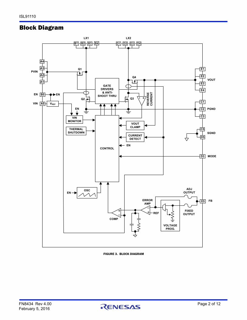
Block Diagram
OSC
ERROR AMP
PVIN
CONTROL
VIN MONITOR
LX1
VREF
REF
RE
VE
RS
E
CU
RR
EN
T
VOUT
D2
GATE DRIVERS & ANTI-
SHOOT THRU
A5VIN
THERMALSHUTDOWN
CURRENTDETECT
E2
B5
EN
E5 FB
C2 PGND
SGND
EN
EN
EN EN
VOUTCLAMP
VOLTAGEPROG.
D1
LX2
E3
C3
D3
COMP
MODE
D3
E1
C1
Q1
Q2 Q3
Q4
ADJ OUTPUT
FIXED OUTPUT
D4B2B1 B3 B4
A2
A1
A3
A4
E4
D5
C5
FIGURE 3. BLOCK DIAGRAM
FN8434 Rev 4.00 Page 2 of 12February 5, 2016

ISL91110
Pin ConfigurationISL91110
(25 BALL WLCSP, 0.4mm PITCH)TOP VIEW, BUMPS DOWN
1 2 3 4 5
A
B
C
D
E
PVIN PVIN PVIN PVIN
LX1 LX1 LX1 LX1
PGND PGND PGND
LX2 LX2 LX2 LX2
VOUT VOUT VOUT VOUT
MODE
VIN
EN
SGND
SGND
FB
Pin DescriptionsPIN # PIN NAMES DESCRIPTION
A1, A2, A3, A4
PVIN Power input; Range: 1.8V to 5.5V. Connect 2x10μF capacitors to PGND.
B1, B2, B3, B4
LX1 Inductor connection, input side
C1, C2, C3 PGND Power ground for high switching current
D1, D2, D3, D4
LX2 Inductor connection, output side
E1, E2,E3, E4
VOUT Buck-boost regulator output; Connect 2x22μF capacitors to PGND.
C4 MODE Logic input, HIGH for auto PFM mode. LOWfor forced PWM operation. Also, this pin canbe used with an external clock sync input.Range: 2.75MHz to 3.25MHz.
A5 VIN Supply input; Range: 1.8V to 5.5V.
B5 EN Logic input, drive HIGH to enable device.
C5, D5 SGND Analog ground pin
E5 FB Voltage feedback pin
Ordering InformationPART NUMBER(Notes 1, 2, 3)
PARTMARKING
OUTPUT VOLTAGE(V)
TAPE AND REEL OPTIONS
TEMP RANGE(°C)
PACKAGE(RoHS Compliant)
PKG. DWG. #
ISL91110IINZ-T 110N 3.3 3k -40 to +85 25 Ball WLCSP W5x5.25E
ISL91110IINZ-T7A 110N 3.3 250 -40 to +85 25 Ball WLCSP W5x5.25E
ISL91110II2AZ-T 102A 3.5 3k -40 to +85 25 Ball WLCSP W5x5.25E
ISL91110II2AZ-T7A 102A 3.5 250 -40 to +85 25 Ball WLCSP W5x5.25E
ISL91110IIAZ-T 110A ADJ 3k -40 to +85 25 Ball WLCSP W5x5.25E
ISL91110IIAZ-T7A 110A ADJ 250 -40 to +85 25 Ball WLCSP W5x5.25E
ISL91110IIA-EVZ Evaluation Board for ISL91110IIAZ
NOTES:
1. Please refer to TB347 for details on reel specifications.
2. These Intersil Pb-free WLCSP and BGA packaged products employ special Pb-free material sets; molding compounds/die attach materials and SnAgCu - e1 solder ball terminals, which are RoHS compliant and compatible with both SnPb and Pb-free soldering operations. Intersil Pb-free WLCSP and BGA packaged products are MSL classified at Pb-free peak reflow temperatures that meet or exceed the Pb-free requirements of IPC/JEDEC J STD-020.
3. For Moisture Sensitivity Level (MSL), please see product information page for ISL91110. For more information on MSL please see techbrief TB363.
TABLE 1. KEY DIFFERENCES BETWEEN FAMILY OF PARTS
PART NUMBER PEAK CURRENT LIMIT rDS(ON) PFET rDS(ON) NFET HICCUP MODE PACKAGETHERMAL
RESISTANCE
ISL91110 4.5A 40mΩ 30mΩ Yes 25-bump 2.33x2.07mm WLCSP JB 13 C/W
ISL91110IR 5.4A 47mΩ 40mΩ No 20 Ld 4x4mm TQFN JC 4 C/W
FN8434 Rev 4.00 Page 3 of 12February 5, 2016

ISL91110
Absolute Maximum Ratings Thermal InformationPVIN, VIN . . . . . . . . . . . . . . . . . . . . . . . . . . . . . . . . . . . . . . . . . . . -0.3V to 6.5VLX1, LX2. . . . . . . . . . . . . . . . . . . . . . . . . . . . . . . . . . . . . . . . . . . . -0.3V to 6.5VFB (Adjustable Version) . . . . . . . . . . . . . . . . . . . . . . . . . . . . . . . -0.3V to 2.7VFB (Fixed VOUT Versions) . . . . . . . . . . . . . . . . . . . . . . . . . . . . . . -0.3V to 6.5VGND, PGND . . . . . . . . . . . . . . . . . . . . . . . . . . . . . . . . . . . . . . . . . -0.3V to 0.3VAll Other Pins . . . . . . . . . . . . . . . . . . . . . . . . . . . . . . . . . . . . . . . -0.3V to 6.5VESD Rating
Human Body Model (Tested per JESD22-A114E) . . . . . . . . . . . . . . . . 3kVMachine Model (Tested per JESD22-A115-A) . . . . . . . . . . . . . . . . . 250V
Latch-Up (Tested per JESD-78B; Class 2, Level A) . . . . . . . . . . . . . . 100mA
Thermal Resistance (Typical) JA (°C/W) JB (°C/W)25 Ball WLCSP Package (Notes 4, 5) . . . . 66 13
Maximum Junction Temperature . . . . . . . . . . . . . . . . . . . . . . . . . . . .+125°CStorage Temperature Range. . . . . . . . . . . . . . . . . . . . . . . .-65°C to +150°CPb-Free Reflow Profile . . . . . . . . . . . . . . . . . . . . . . . . . . . . . . . . . . see TB493
Recommended Operating ConditionsAmbient Temperature Range . . . . . . . . . . . . . . . . . . . . . . . . -40°C to +85°CSupply Voltage Range . . . . . . . . . . . . . . . . . . . . . . . . . . . . . . . . . 1.8V to 5.5VMax Load Current (VIN = 2.5V VOUT = 3.3V) . . . . . . . . . . . . . . . . . . . . .2ADCMax Load Current (VIN = 3.0V VOUT = 3.3V, tON = 600µs, t = 4.6ms). . . . . . 3A
CAUTION: Do not operate at or near the maximum ratings listed for extended periods of time. Exposure to such conditions may adversely impact productreliability and result in failures not covered by warranty.
NOTES:
4. JA is measured in free air with the component mounted on a high effective thermal conductivity test board with “direct attach” features. See Tech Brief TB379.
5. For JB, the board temp is taken on the board near the edge of the package, on a trace at the middle of one side. See Tech Brief TB379.
Analog Specifications VIN = VPVIN = VEN = 3.6V, VOUT = 3.3V, L1 = 1µH, C1 = 2x10µF, C2 = 2x22µF, TA = +25°C. Boldface limits apply across the operating temperature range, -40°C to +85°C and input voltage range (1.8V to 5.5V) unless specified otherwise.
SYMBOL PARAMETER TEST CONDITIONSMIN
(Note 6)TYP
(Note 7)MAX
(Note 6) UNIT
POWER SUPPLY
VIN Input Voltage Range 1.8 5.5 V
VUVLO VIN Undervoltage Lockout Threshold Rising 1.725 1.775 V
Falling 1.550 1.650 V
IVIN VIN Supply Current PFM mode, no external load on VOUT (Note 8) 35 60 µA
ISD VIN Supply Current, Shutdown EN = GND, VIN = 3.6V 0.05 1.00 µA
OUTPUT VOLTAGE REGULATION
VOUT Output Voltage Range ISL91110IIAZ, IOUT = 100mA, VIN = 3.6V 1.00 5.20 V
Output Voltage Accuracy VIN = 3.7V, VOUT = 3.3V, IOUT = 0mA, PWM mode -2 +2 %
VIN = 3.7V, VOUT = 3.3V, IOUT = 1mA, PFM mode -3 +4 %
VFB FB Pin Voltage Regulation For adjustable output version, VIN = 3.6V 0.783 0.800 0.813 V
IFB FB Pin Bias Current For adjustable output version 20 nA
VOUT/VIN
Line Regulation, PWM Mode IOUT = 500mA, VOUT = 3.3V, VIN step from 2.3V to 5.5V
±5 mV/V
VOUT/IOUT
Load Regulation, PWM Mode VIN = 3.7V, VOUT = 3.3V, IOUT step from 0mA to 1000mA
±0.005 mV/mA
VOUT/VI
Line Regulation, PFM Mode IOUT = 100mA, VOUT = 3.3V, VIN step from 2.3V to 5.5V
±12.5 mV/V
VOUT/IOUT
Load Regulation, PFM Mode VIN = 3.7V, VOUT = 3.3V, IOUT step from 0mA to 100mA
±0.4 mV/mA
VCLAMP Output Voltage Clamp Rising 5.25 5.95 V
Output Voltage Clamp Hysteresis 400 mV
DC/DC SWITCHING SPECIFICATIONS
fSW Oscillator Frequency 2.10 2.50 2.90 MHz
tONMIN Minimum On Time 80 ns
IPFETLEAK LX1 Pin Leakage Current VIN = 3.6V -1 1 µA
INFETLEAK LX2 Pin Leakage Current VIN = 3.6V -1 1 µA
FN8434 Rev 4.00 Page 4 of 12February 5, 2016

ISL91110
SOFT-START AND SOFT DISCHARGE
tSS Soft-Start Time Time from when EN signal asserts to when output voltage ramp starts.
1 ms
Time from when output voltage ramp starts to when output voltage reaches 95% of its nominal value with device operating in buck mode.VIN = 4V, VOUT = 3.3V, IO = 200mA
1 ms
Time from when output voltage ramp starts to when output voltage reaches 95% of its nominal value with device operating in boost mode.VIN = 2V, VOUT = 3.3V, IO = 200mA
2 ms
RDISCHG VOUT Soft-Discharge ON-Resistance EN < VIL 120 Ω
POWER MOSFET
RDSON_P P-Channel MOSFET ON-Resistance VIN = 3.6V, IO = 200mA 40 mΩ
VIN = 2.5V, IO = 200mA 55 mΩ
RDSON_N N-Channel MOSFET ON-Resistance VIN = 3.6V, IO = 200mA 30 mΩ
VIN = 2.5V, IO = 200mA 45 mΩ
IPK_LMT P-Channel MOSFET Peak Current Limit 3.9 4.5 5.1 A
PFM/PWM TRANSITION
Load Current Threshold, PFM to PWM VIN = 3.6V, VOUT = 3.3V 200 mA
Load Current Threshold, PWM to PFM VIN = 3.6V, VOUT = 3.3V 75 mA
Thermal Shutdown 155 °C
Thermal Shutdown Hysteresis 30 °C
LOGIC INPUTS
ILEAK Input Leakage VIN = 3.6V 0.05 1.00 µA
VIH Input HIGH Voltage VIN = 3.6V 1.4 V
VIL Input LOW Voltage VIN = 3.6V 0.4 V
NOTES:
6. Parameters with MIN and/or MAX limits are 100% tested at +25°C, unless otherwise specified. Temperature limits established by characterization and are not production tested.
7. Typical values are for TA = +25°C and VIN = 3.6V.
8. Quiescent current measurements are taken when the output is not switching.
Analog Specifications VIN = VPVIN = VEN = 3.6V, VOUT = 3.3V, L1 = 1µH, C1 = 2x10µF, C2 = 2x22µF, TA = +25°C. Boldface limits apply across the operating temperature range, -40°C to +85°C and input voltage range (1.8V to 5.5V) unless specified otherwise. (Continued)
SYMBOL PARAMETER TEST CONDITIONSMIN
(Note 6)TYP
(Note 7)MAX
(Note 6) UNIT
FN8434 Rev 4.00 Page 5 of 12February 5, 2016

ISL91110
Typical Performance Curves Unless otherwise noted, operating conditions are: TA = +25°C, VIN = EN = 3.6V, L = 1µH, C1 = 2x10µF, C2 = 2x22µF, VOUT = 3.3V, IOUT = 0A to 3A
FIGURE 4. EFFICIENCY vs INPUT VOLTAGE FIGURE 5. OUTPUT VOLTAGE vs LOAD CURRENT
FIGURE 6. QUIESCENT CURRENT vs INPUT VOLTAGE (VOUT = 3.3V, MODE = HIGH)
FIGURE 7. SWITCHING FREQUENCY vs INPUT VOLTAGE
FIGURE 8. STEADY-STATE OPERATION IN PFM (VIN = 4V, VOUT = 3.3V, NO LOAD)
FIGURE 9. STEADY-STATE OPERATION IN PWM (VIN = 3.3V, VOUT = 3.3V, NO LOAD)
80
82
84
86
88
90
92
94
96
98
100
2 3 4 5
EF
FIC
IEN
CY
(%
)
VIN (V)
LOAD = 10mA
LOAD = 1000mA
LOAD = 500mALOAD = 100mA
3.26
3.27
3.28
3.29
3.30
3.31
3.32
1 10 100 1000LOAD CURRENT (mA)
VO
UT (
V)
VIN = 3.0V
VIN = 3.6V
VIN = 2.5V
VIN = 4.0V
VIN = 4.5V
TA = -40°C
TA = +25°CTA = +85°C
0
10
20
30
40
50
60
70
80
1.5 2.5 3.5 4.5 5.5VIN (V)
QU
IES
CE
NT
CU
RR
EN
T (
µA
)
2.25
2.30
2.35
2.40
2.45
2.50
2.55
1.5 2.5 3.5 4.5 5.5VIN (V)
SW
ITC
HIN
G F
RE
QU
EN
CY
(M
Hz)
LX1 (2V/DIV)
LX2 (2V/DIV)
VOUT (AC, 50mV/DIV)
IL (500mA/DIV)
400ns/DIV 400ns/DIV
LX1 (2V/DIV)
LX2 (2V/DIV)
VOUT (AC, 10mV/DIV)
IL (200mA/DIV)
FN8434 Rev 4.00 Page 6 of 12February 5, 2016

ISL91110
FIGURE 10. SOFT-START (VIN = 3.6V, VOUT = 3.3V, NO LOAD) FIGURE 11. SOFT-START (VIN = 3.6V, VOUT = 3.3V, 1A R-LOAD)
FIGURE 12. STEADY STATE OPERATION (VIN = 2.5V, VOUT = 3.3V,2A LOAD)
FIGURE 13. 0A TO 2A LOAD TRANSIENT (VIN = 3.6V, VOUT = 3.3V)
FIGURE 14. 0.5A TO 1.5A LOAD TRANSIENT (VIN = 3.6V, VOUT = 3.3V) FIGURE 15. 0A TO 1A LOAD TRANSIENT (VIN = 3.6V, VOUT = 3.3V)
Typical Performance Curves Unless otherwise noted, operating conditions are: TA = +25°C, VIN = EN = 3.6V, L = 1µH, C1 = 2x10µF, C2 = 2x22µF, VOUT = 3.3V, IOUT = 0A to 3A (Continued)
IL (500mA/DIV)
400µs/DIV
VOUT (1V/DIV)
EN (2V/DIV)
IL (500mA/DIV)
400µs/DIV
VOUT (1V/DIV)
EN (2V/DIV)
VOUT (AC, 20mV/DIV)
LX1 (2V/DIV)
LX2 (2V/DIV)
IL (1A/DIV)
400ns/DIV 100µs/DIV
VOUT (AC, 100mV/DIV)
IL (1A/DIV)
VOUT (AC, 100mV/DIV)
IL (500mA/DIV)
100µs/DIV
VOUT (AC, 50mV/DIV)
IL (500mA/DIV)
100µs/DIV
FN8434 Rev 4.00 Page 7 of 12February 5, 2016

ISL91110
Functional DescriptionFunctional OverviewRefer to the “Block Diagram” on page 2. The ISL91110 implements a complete buck-boost switching regulator, with PWM controller, internal switches, references, protection circuitry and control inputs.
The PWM controller automatically switches between buck and boost modes as necessary to maintain a steady output voltage, with changing input voltages and dynamic external loads.
Internal Supply and ReferencesReferring to the “Block Diagram” on page 2, the ISL91110 provides four power input pins. The PVIN pin supplies input power to the DC/DC converter, while the VIN pin provides operating voltage source required for stable VREF generation. Separate ground pins (GND and PGND) are provided to avoid problems caused by ground shift due to the high switching currents.
Enable InputThe device is enabled by asserting the EN pin HIGH. Driving EN LOW invokes a power-down mode, where most internal device functions are disabled.
Soft DischargeWhen the device is disabled by driving EN LOW, an internal resistor between VOUT and GND is activated to slowly discharge the output capacitor. This internal resistor has a typical 120Ω resistance.
POR Sequence and Soft-StartAsserting the EN pin HIGH allows the device to power up. A number of events occur during the start-up sequence. The internal voltage reference powers up, and stabilizes. The device then starts operating. There is a typical 1ms delay between assertion of the EN pin and the start of switching regulator soft-start ramp.
The soft-start feature minimizes output voltage overshoot and input inrush currents. During soft-start, the reference voltage is ramped to provide a ramping VOUT voltage. While the output voltage is lower than approximately 20% of the target output voltage, switching frequency is reduced to a fraction of the normal switching frequency to aid in producing low duty cycles necessary to avoid input inrush current spikes. Once the output voltage exceeds 20% of the target voltage, switching frequency is increased to its nominal value.
When the target output voltage is higher than the input voltage, there will be a transition from buck mode to boost mode during the soft-start sequence. At the time of this transition, the ramp rate of the reference voltage is decreased, such that the output voltage slew rate is decreased. This provides a slower output voltage slew rate.
The VOUT ramp time is not constant for all operating conditions. Soft-start into boost mode will take longer than soft-start into buck mode. The total soft-start time into buck operating mode is typically 2ms, whereas the typical soft-start time into boost mode operating mode is typically 3ms. Increasing the load current will increase these typical soft-start times.
Overcurrent ProtectionThe ISL91110 provides short-circuit protection by monitoring the feedback voltage. When feedback voltage is sensed to be lower than a certain threshold, the PWM oscillator frequency is reduced in order to protect the device from damage. The P-Channel MOSFET peak current limit remains active during this state.
When the current in the P-Channel MOSFET is sensed to reach the current limit for 16 consecutive switching cycles, the internal protection circuit is triggered, and switching is stopped for approximately 40ms. The device then performs a soft-start cycle. If the external output overcurrent condition exists after the soft-start cycle, the device will again detect 16 consecutive switching cycles reaching the peak current threshold and turns off for 40ms. The process will repeat as long as the external overcurrent condition is present. This behavior is called “hiccup mode”.
FIGURE 16. OUTPUT SHORT-CIRCUIT BEHAVIOR (VIN = 3.6V, VOUT = 3.3V)
FIGURE 17. 4V TO 3.2V LINE TRANSIENT (VOUT = 3.3V, LOAD = 1A)
Typical Performance Curves Unless otherwise noted, operating conditions are: TA = +25°C, VIN = EN = 3.6V, L = 1µH, C1 = 2x10µF, C2 = 2x22µF, VOUT = 3.3V, IOUT = 0A to 3A (Continued)
LX2 (2V/DIV)
VOUT (1V/DIV)
IL (1A/DIV)
LX1 (2V/DIV)
20ms/DIV
VOUT (AC, 100mV/DIV)
10µs/DIV
VIN (1V/DIV)
FN8434 Rev 4.00 Page 8 of 12February 5, 2016

ISL91110
Thermal ShutdownA built-in thermal protection feature protects the ISL91110 if the die temperature reaches +155°C (typical). At this die temperature, the regulator is completely shut down. The die temperature continues to be monitored in this thermal shutdown mode. When the die temperature falls to +125°C (typical), the device will resume normal operation. When exiting thermal shutdown, the ISL91110 will execute its soft-start sequence.
Buck-Boost Conversion TopologyThe ISL91110 operates in either buck or boost mode. When operating in conditions where PVIN is close to VOUT, ISL91110 alternates between buck and boost mode as necessary to provide a regulated output voltage.
Figure 18 shows a simplified diagram of the internal switches and external inductor.
PWM OperationIn buck PWM mode, Switch D is continuously closed, and Switch C is continuously open. Switches A and B operate as a synchronous buck converter when in this mode.
In boost PWM mode, Switch A remains closed and Switch B remains open. Switches C and D operate as a synchronous boost converter when in this mode.
PFM OperationDuring PFM operation in buck mode, Switch D is continuously closed and Switch C is continuously open. Switches A and B operate in discontinuous mode during PFM operation. During PFM operation in boost mode, the ISL91110 closes Switch A and Switch C to ramp up the current in the inductor. When the inductor current reaches a certain threshold, the device turns off Switches A and C, then turns on Switches B and D. With Switches B and D closed, output voltage increases as the inductor current ramps down.
In most operating conditions, there will be multiple PFM pulses to charge up the output capacitor. These pulses continue until VOUT has achieved the upper threshold of the PFM hysteretic controller. Switching then stops, and remains stopped until VOUT decays to the lower threshold of the hysteretic PFM controller.
Operation With VIN Close to VOUTWhen the output voltage is close to the input voltage, the ISL91110 will rapidly and smoothly switch from boost to buck
mode as needed to maintain the regulated output voltage. This behavior provides excellent efficiency and very low output voltage ripple.
Output Voltage ProgrammingThe ISL91110 is available in fixed and adjustable output voltage versions. To use the fixed output version, the VOUT pin must be connected directly to FB.
In the adjustable output voltage version (ISL91110IIAZ), an external resistor divider is required to program the output voltage. The FB pin has very low input leakage current, so it is possible to use large value resistors (e.g., R1 = 1MΩ and R2 = 324kΩ for VOUT = 3.3V) in the resistor divider connected to the FB input.
Applications InformationComponent SelectionThe fixed-output version of ISL91110 requires only three external power components to implement the buck boost converter: an inductor, an input capacitor and an output capacitor.
The adjustable output version of ISL91110 requires three additional components to program the output voltage, as shown in Figure 19. Two external resistors program the output voltage, and a small capacitor is added to improve stability and response.
Output Voltage Programming, Adjustable VersionWhen VREF is connected to GND, setting and controlling the output voltage of the ISL91110IIAZ (adjustable output version) can be accomplished by selecting the external resistor values.
Equation 1 can be used to derive the R1 and R2 resistor values:
When designing a PCB, include a GND guard band around the feedback resistor network to reduce noise and improve accuracy and stability. Resistors R1 and R2 should be positioned close to the FB pin.
Feed-Forward Capacitor Selection A small capacitor (C3 in Figure 19) in parallel with resistor R1 is required to provide the specified load and line regulation. The suggested value of this capacitor is 56pF for R1 = 1MΩ. An NPO type capacitor is recommended.
FIGURE 18. BUCK BOOST TOPOLOGY
PVIN VOUT
SWITCH A SWITCH D
SWITCH B SWITCH C
LX1 LX2
L1
PVIN
VIN =1.8V TO 5.5V
VOUT = 1V TO 5.2VUP TO 3A
ISL91110IIAZ
VIN
EN
LX1
LX2
VOUT
FB
SG
ND
PG
ND
C12x10µF
L11µH
C22x22µF
MODE
R1
R2
C3
FIGURE 19. ADJUSTABLE OUTPUT APPLICATION
VOUT 0.8V 1R1R2-------+
= (EQ. 1)
FN8434 Rev 4.00 Page 9 of 12February 5, 2016
ISL91110
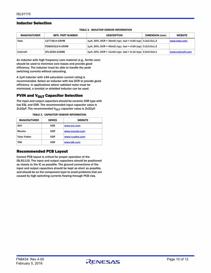
Inductor Selection
An inductor with high frequency core material (e.g., ferrite core) should be used to minimize core losses and provide good efficiency. The inductor must be able to handle the peak switching currents without saturating.
A 1µH inductor with ≥4A saturation current rating is recommended. Select an inductor with low DCR to provide good efficiency. In applications where radiated noise must be minimized, a toroidal or shielded inductor can be used.
PVIN and VOUT Capacitor Selection The input and output capacitors should be ceramic X5R type with low ESL and ESR. The recommended input capacitor value is 2x10µF. The recommended VOUT capacitor value is 2x22µF.
Recommended PCB LayoutCorrect PCB layout is critical for proper operation of the ISL91110. The input and output capacitors should be positioned as closely to the IC as possible. The ground connections of the input and output capacitors should be kept as short as possible, and should be on the component layer to avoid problems that are caused by high switching currents flowing through PCB vias.
TABLE 2. INDUCTOR VENDOR INFORMATION
MANUFACTURER MFR. PART NUMBER DESCRIPTION DIMENSION (mm) WEBSITE
Toko 1277AS-H-1R0M 1µH, 20%, DCR = 34mΩtypIsat = 4.6A (typ) 3.2x2.5x1.2 www.toko.com
FDSD0312-H-1R0M 1µH, 20%, DCR = 43mΩtypIsat = 4.5A (typ) 3.2x3.0x1.2
Coilcraft XFL4020-102ME 1µH, 20%, DCR = 11mΩtypIsat = 5.1A (typ) 4.0x4.0x2.1 www.coilcraft.com
TABLE 3. CAPACITOR VENDOR INFORMATION
MANUFACTURER SERIES WEBSITE
AVX X5R www.avx.com
Murata X5R www.murata.com
Taiyo Yuden X5R www.t-yuden.com
TDK X5R www.tdk.com
FN8434 Rev 4.00 Page 10 of 12February 5, 2016
ISL91110
Intersil products are manufactured, assembled and tested utilizing ISO9001 quality systems as notedin the quality certifications found at www.intersil.com/en/support/qualandreliability.html
Intersil products are sold by description only. Intersil may modify the circuit design and/or specifications of products at any time without notice, provided that such modification does not, in Intersil's sole judgment, affect the form, fit or function of the product. Accordingly, the reader is cautioned to verify that datasheets are current before placing orders. Information furnished by Intersil is believed to be accurate and reliable. However, no responsibility is assumed by Intersil or its subsidiaries for its use; nor for any infringements of patents or other rights of third parties which may result from its use. No license is granted by implication or otherwise under any patent or patent rights of Intersil or its subsidiaries.
For information regarding Intersil Corporation and its products, see www.intersil.com
For additional products, see www.intersil.com/en/products.html
© Copyright Intersil Americas LLC 2013-2016. All Rights Reserved.All trademarks and registered trademarks are the property of their respective owners.
About IntersilIntersil Corporation is a leading provider of innovative power management and precision analog solutions. The company's products address some of the largest markets within the industrial and infrastructure, mobile computing and high-end consumer markets.
For the most updated datasheet, application notes, related documentation and related parts, please see the respective product information page found at www.intersil.com.
You may report errors or suggestions for improving this datasheet by visiting www.intersil.com/ask.
Reliability reports are also available from our website at www.intersil.com/support.
Revision HistoryThe revision history provided is for informational purposes only and is believed to be accurate, but not warranted. Please go to web to make sure you have the latest revision.
DATE REVISION CHANGE
February 5, 2016 FN8434.4 Added Note to Figure 1 on page 1.Updated pin configuration on page 3 by adding labels.Added Table 1 on page 3.
November 20, 2014 FN8434.3 On page 8, "Short Circuit Protection" section title was updated to "Overcurrent Protection." Also in the newly titled "Overcurrent Protection" section, a paragraph was added to explain hiccup mode operation.
October 28, 2014 FN8434.2 On Page 1, 3rd paragraph, changed output as low as 0.8V, as high as 5.25V to: "changed output as low as 1.0V, as high as 5.2V". The IC label on Figure 19 changed from ISL91110INZ to ISL91110IIAZTjb changed from 14 to 13 in Thermal information.
August 22, 2014 FN8434.1 Updated Figure 1 on page 1, Changed text from “"Li-ion Battery 2.5V to 4.35V" to "VIN = 1.8V TO 5.5V" and "MAX. IOUT = 2A (Min)" to "IOUT = UP TO 3A"Replaced Figure 2 on page 1.Added -T7A parts to the “Ordering Information” table on page 3.Changed “IFB” on page 4, max spec from “1µA to 20nA”.Changed Section title on page 5 from “EN LOGIC INPUTS” to “LOGIC INPUTS”.Added “Typical Performance Curves” on page 6.Changed text on Figure 19 on page 9, from "VOUT=0.8V TO 5.25V, UP TO 3A" to "VOUT = 1V to 5.2V, UP TO 3A"Replaced “Package Outline Drawing” on page 12.
December 24, 2013 FN8434.0 Initial Release.
FN8434 Rev 4.00 Page 11 of 12February 5, 2016

ISL91110
FN8434 Rev 4.00 Page 12 of 12February 5, 2016
Package Outline DrawingW5x5.25E5X5 ARRAY 25 BALLS WITH 0.40 PITCH WAFER LEVEL CHIP SCALE PACKAGE (With BSC)
Rev 0, 1/14
BOTTOM VIEW
TYPICAL RECOMMENDED LAND PATTERN
TOP VIEW
NSMD refers to Non-Solder Mask Defined pad design per
Dimension and tolerance per ASMEY 14.5M-1994,
3.
2.
All dimensions are in millimeters.1.
NOTES:
and JESD 95-1 SPP-010.
Intersil Tech Brief TB451 located at:http://www.intersil.com/content/dam/Intersil/docu-ments/tb45/tb451.pdf
SIDE VIEW
0.10 Z X Y0.05 Z
2.070 ± 0.030
2.330 ± 0.030
Y X
(4X)0.10
PIN 1 (A1 CORNER)
25x 0.265 ± 0.035
0.400
E
D
C
B
A
0.400
1 2 3 4 5
0.235
0.365
1.600
0.240
PACKAGE OUTLINE
0.400
0.290
NSMD3
0.0400 BSC(BACK SIDE COATING)
0.200 ± 0.03
0.265 ± 0.035
SEATING PLANE
0.05 Z
0.540 ± 0.050
3
Z