
ISCA 2015 ShiDianNao
13
ShiDianNao: Shifting Vision Processing Closer to the Sensor Zidong Du †] Robert Fasthuber ‡ Tianshi Chen † Paolo Ienne ‡ Ling Li † Tao Luo †] Xiaobing Feng † Yunji Chen † Olivier Temam § † State Key Laboratory of Computer Architecture, Institute of Computing Technology (ICT), CAS, China ] University of CAS, China ‡ EPFL, Switzerland § Inria, France {duzidong,chentianshi,liling,luotao,fxb,cyj}@ict.ac.cn {robert.fasthuber,paolo.ienne}@epfl.ch [email protected] Abstract In recent years, neural network accelerators have been shown to achieve both high energy efficiency and high per- formance for a broad application scope within the important category of recognition and mining applications. Still, both the energy efficiency and performance of such accelerators remain limited by memory accesses. In this paper, we focus on image applications, arguably the most important category among recognition and mining applications. The neural networks which are state-of-the-art for these applica- tions are Convolutional Neural Networks (CNN), and they have an important property: weights are shared among many neurons, considerably reducing the neural network memory footprint. This property allows to entirely map a CNN within an SRAM, eliminating all DRAM accesses for weights. By further hoisting this accelerator next to the image sensor, it is possible to eliminate all remaining DRAM accesses, i.e., for inputs and outputs. In this paper, we propose such a CNN accelerator, placed next to a CMOS or CCD sensor. The absence of DRAM ac- cesses combined with a careful exploitation of the specific data access patterns within CNNs allows us to design an ac- celerator which is 60× more energy efficient than the previous state-of-the-art neural network accelerator. We present a full design down to the layout at 65 nm, with a modest footprint of 4.86 mm 2 and consuming only 320 mW , but still about 30× faster than high-end GPUs. 1. Instructions In the past few years, accelerators have gained increasing at- tention as an energy and cost effective alternative to CPUs and GPUs [20, 57, 13, 14, 60, 61]. Traditionally, the main Permission to make digital or hard copies of all or part of this work for personal or classroom use is granted without fee provided that copies are not made or distributed for profit or commercial advantage and that copies bear this notice and the full citation on the first page. Copyrights for components of this work owned by others than ACM must be honored. Abstracting with credit is permitted. To copy otherwise, or republish, to post on servers or to redistribute to lists, requires prior specific permission and/or a fee. Request permissions from [email protected]. ISCA’15, June 13 - 17, 2015, Portland, OR, USA Copyright 2015 ACM 978-1-4503-3402-0/15/06$15.00 http://dx.doi.org/10.1145/2749469.2750389 downside of accelerators is their limited application scope, but recent research in both academia and industry has highlighted the remarkable convergence of trends towards recognition and mining applications [39] and the fact that a very small corpus of algorithms—i.e., neural network based algorithms—can tackle a significant share of these applications [7, 41, 24]. This makes it possible to realize the best of both worlds: ac- celerators with high performance/efficiency and yet broad application scope. Chen et al. [3] leveraged this fact to pro- pose neural network accelerators; however, the authors also acknowledge that, like many processing architectures, their accelerator efficiency and scalability remains severely limited by memory bandwidth constraints. That study aimed at supporting the two main state-of-the-art neural networks: Convolutional Neural Networks (CNNs) [35] and Deep Neural Networks (DNNs) [32, 48]. Both types of networks are very popular, with DNNs being more general than CNNs due to one major difference: in CNNs, it is as- sumed that each neuron (of a feature map, see later Section 3 for more details) shares its weights with all other neurons, making the total number of weights far smaller than in DNNs. For instance, the largest state-of-the-art CNN has 60 millions weights [29] versus up to 1 billion [34] or even 10 billions [6] for the largest DNNs. Such weight sharing property directly derives from the CNN application scope, i.e., vision recogni- tion applications: since the set of weights feeding a neuron characterizes the feature this neuron should recognize, sharing weights is simply a way to express that any feature can appear anywhere within an image [35], i.e., translation invariance. Now, this simple property can have profound implications for architects: It is well known that the highest energy expense is related to data movement, in particular DRAM accesses, rather than computation [20, 28]. Due to its small weights memory footprint, it is possible to store a whole CNN within a small SRAM next to computational operators, and as a result, there is no longer a need for DRAM memory accesses to fetch the model (weights) in order to process each input. The only remaining DRAM accesses become those needed to fetch the input image. Unfortunately, when the input is as large as an image, this would still constitute a large energy expense. However, CNNs are dedicated to image applications, which, arguably, constitute one of the broadest categories of recog- 92
-
Upload
steven-song -
Category
Documents
-
view
298 -
download
27
Transcript of ISCA 2015 ShiDianNao
ShiDianNao: Shifting Vision Processing Closer to the Sensor
Zidong Du†] Robert Fasthuber‡ Tianshi Chen† Paolo Ienne‡ Ling Li† Tao Luo†]
Xiaobing Feng† Yunji Chen† Olivier Temam§
†State Key Laboratory of Computer Architecture, Institute of Computing Technology (ICT), CAS, China]University of CAS, China ‡EPFL, Switzerland §Inria, France
{duzidong,chentianshi,liling,luotao,fxb,cyj}@ict.ac.cn
{robert.fasthuber,paolo.ienne}@epfl.ch [email protected]
AbstractIn recent years, neural network accelerators have been
shown to achieve both high energy efficiency and high per-formance for a broad application scope within the importantcategory of recognition and mining applications.
Still, both the energy efficiency and performance of suchaccelerators remain limited by memory accesses. In this paper,we focus on image applications, arguably the most importantcategory among recognition and mining applications. Theneural networks which are state-of-the-art for these applica-tions are Convolutional Neural Networks (CNN), and theyhave an important property: weights are shared among manyneurons, considerably reducing the neural network memoryfootprint. This property allows to entirely map a CNN withinan SRAM, eliminating all DRAM accesses for weights. Byfurther hoisting this accelerator next to the image sensor, it ispossible to eliminate all remaining DRAM accesses, i.e., forinputs and outputs.
In this paper, we propose such a CNN accelerator, placednext to a CMOS or CCD sensor. The absence of DRAM ac-cesses combined with a careful exploitation of the specificdata access patterns within CNNs allows us to design an ac-celerator which is 60× more energy efficient than the previousstate-of-the-art neural network accelerator. We present a fulldesign down to the layout at 65 nm, with a modest footprintof 4.86 mm2 and consuming only 320 mW, but still about 30×faster than high-end GPUs.
1. InstructionsIn the past few years, accelerators have gained increasing at-tention as an energy and cost effective alternative to CPUsand GPUs [20, 57, 13, 14, 60, 61]. Traditionally, the main
Permission to make digital or hard copies of all or part of this work forpersonal or classroom use is granted without fee provided that copies are notmade or distributed for profit or commercial advantage and that copies bearthis notice and the full citation on the first page. Copyrights for componentsof this work owned by others than ACM must be honored. Abstracting withcredit is permitted. To copy otherwise, or republish, to post on servers or toredistribute to lists, requires prior specific permission and/or a fee. Requestpermissions from [email protected]’15, June 13 - 17, 2015, Portland, OR, USACopyright 2015 ACM 978-1-4503-3402-0/15/06$15.00http://dx.doi.org/10.1145/2749469.2750389
downside of accelerators is their limited application scope, butrecent research in both academia and industry has highlightedthe remarkable convergence of trends towards recognition andmining applications [39] and the fact that a very small corpusof algorithms—i.e., neural network based algorithms—cantackle a significant share of these applications [7, 41, 24].This makes it possible to realize the best of both worlds: ac-celerators with high performance/efficiency and yet broadapplication scope. Chen et al. [3] leveraged this fact to pro-pose neural network accelerators; however, the authors alsoacknowledge that, like many processing architectures, theiraccelerator efficiency and scalability remains severely limitedby memory bandwidth constraints.
That study aimed at supporting the two main state-of-the-artneural networks: Convolutional Neural Networks (CNNs) [35]and Deep Neural Networks (DNNs) [32, 48]. Both types ofnetworks are very popular, with DNNs being more generalthan CNNs due to one major difference: in CNNs, it is as-sumed that each neuron (of a feature map, see later Section3 for more details) shares its weights with all other neurons,making the total number of weights far smaller than in DNNs.For instance, the largest state-of-the-art CNN has 60 millionsweights [29] versus up to 1 billion [34] or even 10 billions [6]for the largest DNNs. Such weight sharing property directlyderives from the CNN application scope, i.e., vision recogni-tion applications: since the set of weights feeding a neuroncharacterizes the feature this neuron should recognize, sharingweights is simply a way to express that any feature can appearanywhere within an image [35], i.e., translation invariance.
Now, this simple property can have profound implicationsfor architects: It is well known that the highest energy expenseis related to data movement, in particular DRAM accesses,rather than computation [20, 28]. Due to its small weightsmemory footprint, it is possible to store a whole CNN within asmall SRAM next to computational operators, and as a result,there is no longer a need for DRAM memory accesses to fetchthe model (weights) in order to process each input. The onlyremaining DRAM accesses become those needed to fetch theinput image. Unfortunately, when the input is as large as animage, this would still constitute a large energy expense.
However, CNNs are dedicated to image applications, which,arguably, constitute one of the broadest categories of recog-
92
nition applications (followed by voice recognition). In manyreal-world and embedded applications—e.g., smartphones,security, self-driving cars—the image directly comes from aCMOS or CCD sensor. In a typical imaging device, the imageis acquired by the CMOS/CCD sensor, sent to DRAM, andlater fetched by the CPU/GPU for recognition processing. Thesmall size of the CNN accelerator (computational operatorsand SRAM holding the weights) makes it possible to hoist itnext to the sensor, and only send the few output bytes of therecognition process (typically, an image category) to DRAMor the host processor, thereby almost entirely eliminating en-ergy costly accesses to/from memory.
In this paper, we study an energy-efficient design of a vi-sual recognition accelerator to be directly embedded with anyCMOS or CCD sensor, and fast enough to process images inreal time. Our accelerator leverages the specific propertiesof CNN algorithms, and as a result, it is 60× more energyefficient than DianNao [3], which was targeting a broader setof neural networks. We achieve that level of efficiency notonly by eliminating DRAM accesses, but also by carefullyminimizing data movements between individual processingelements, from the sensor, and the SRAM holding the CNNmodel. We present a concrete design, down to the layout,in a 65 nm CMOS technology with a peak performance of194 GOP/s (billions of fixed-point OPerations per second) at4.86 mm2, 320.10 mW , and 1 GHz. We empirically evaluateour design on ten representative benchmarks (neural networklayers) extracted from state-of-the-art CNN implementations.We believe such accelerators can considerably lower the hard-ware and energy cost of sophisticated vision processing, andthus help make them widespread.
The rest of this paper is organized as follows. In Section 2we precisely describe the integration conditions we target forour accelerator, which are determinant in our architecturalchoices. Section 3 is a primer on recent machine-learningtechniques where we introduce the different types of CNN lay-ers. We give a first idea of the mapping principles in Section 4and, in Sections 5 to 7, we introduce the detailed architectureof our accelerator (ShiDianNao, Shi for vision and DianNaofor electronic brain) and discuss design choices. In Section 8,we show how to map CNNs on ShiDianNao and schedule thedifferent layers. In Section 9, the experimental methodologyis described. In Section 10, we implemented ShiDianNaoand compared the results to the state-of-the-art in terms ofperformance and hardware costs. In Section 12, conclusionsare given. Related work is discussed in Section 11.
2. System IntegrationFigure 1 shows a typical integration solution for cheap cameras(closely resembling an STM chipset [55, 56]): An image pro-cessing chip is connected to cameras (in typical smartphones,two) streaming their data through standard Camera Serial In-terfaces (CSIs). Video processing pipelines, controlled by amicrocontroller unit, implement a number of essential func-
Acc
Videopipelines
Micro-Controller
SRAM256KB
GPIO&
I2C
BUS
at (384,768)
"cat"
CSI-2 I/F
CSI-2 I/F
CSI-2 I/F
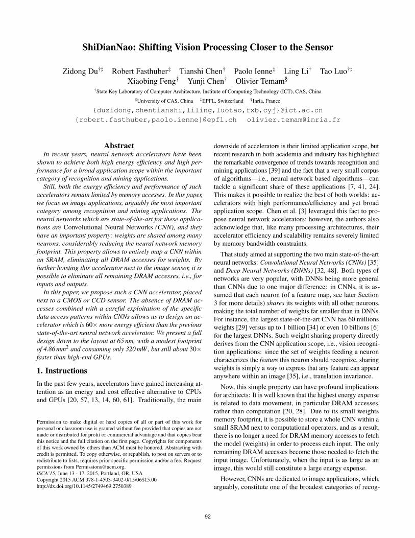
Sensors Image processor Host
Figure 1: Possible integration of our accelerator in a commer-cial image processing chip.
tions such as Bayer reconstruction, white balance and barrelcorrection, noise and defect filtering, autofocus control, videostabilization, and image compression. More advanced pro-cessors already implement rudimentary object detection andtracking functions, such as face recognition [56].
The figure shows also the approximate setting of our ShiDi-anNao accelerator, with high-level control from the embeddedmicrocontroller and using for image input the same memorybuffers. Contrary to the fairly elementary processing of thevideo pipelines, our accelerator is meant to achieve very signif-icantly more advanced classification tasks. One should noticethat, to contain cost and energy consumption, this type of com-mercial image processors go a long way to avoid full-imagebuffering (which, of course, for 8-megapixel images wouldrequire several megabytes of storage): input and outputs ofthe system are through serial streaming channels, there is nointerface to external DRAM, and the local SRAM storage isvery limited (e.g., 256 KB [55]). These constraints are whatwe are going to use to design our system: our recognition sys-tem must also avoid full-frame storage, exclude any externalDRAM interface, and process sequentially a stream of partialframe sections as they flow from the sensors to the applica-tion processor. We will later show (Section 10.2) that a localstorage of 256 KB appears appropriate also for our accelerator.
3. Primer on Convolutional Neural Networks
Convolutional Neural Networks (CNNs) [35] and Deep NeuralNetworks (DNNs) [32] are known as two state-of-the-art ma-chine learning algorithms. Both of them belong to the familyof Multi-Layer Perceptrons (MLPs) [21] and may consist offour types of layers: convolutional, pooling, normalization,and classifier layers. However, the two network types differfrom each other in their convolutional layers—the type of lay-ers dominate the execution time of both types of networks [3].In a CNN convolutional layer, synaptic weights can be reused(shared) by certain neurons, while there is no such reuse ina DNN convolutional layer (see below for details). The datareuse in CNN naturally favors hardware accelerators, becauseit reduces the number of synaptic weights to store, possiblyallowing them to be simultaneously kept on-chip.
General Architecture. Figure 2 illustrates the architectureof LeNet-5 [35], a representative CNN widely used in doc-ument recognition. It consists of two convolutional layers(C1 and C3 in Figure 2), two pooling layers (S2 and S4 in
93

INPUT32x32
C1: feature maps6@28x28
S2: f. maps6@14x14
C3: f. maps 16@10x10
S4: f. maps16@5x5 F5: 120 F6: 84
F7: 10
Convolutional Subsampling
ConvolutionalSubsampling
Full connection
Figure 2: A representative CNN architecture—LeNet5 [35]. C:Convolutional layer; S: Pooling layer; F: Classifier layer.
Figure 2), and three classifier layers (F5, F6 and F7 in Figure2). Recent studies also suggest the use of normalization layersin deep learning [29, 26].
Convolutional Layer. A convolutional layer can be viewedas a set of local filters designed for identifying certain char-acteristics of input feature maps (i.e., 2D arrays of input pix-els/neurons). Each local filter has a kernel having Kx×Kycoefficients, and processes a convolutional window capturingKx×Ky input neurons in one input feature map (or multiplesame-sized windows in multiple input feature maps). A 2Darray of local filters produces an output feature map, whereeach local filter corresponds to an output neuron, and convo-lutional windows of adjacent output neurons are sliding bysteps of Sx (x-direction) and Sy (y-direction) in the same inputfeature map. Formally, the output neuron at position (a,b) ofthe output feature map #mo is computed with
Omoa,b = f
(∑
mi∈Amo
(β
mi,mo +Kx−1
∑i=0
Ky−1
∑j=0
ωmi,moi, j × Imi
aSx+i,bSy+ j
)), (1)
where ωmi,mo is the kernel between input feature map #mi andoutput feature map #mo, β mi,mo is the bias value for the pair ofinput and output feature maps, Amo is the set of input featuremaps connected to output feature map #mo, and f ( ·) is thenon-linear activation function (e.g., tanh or sigmoid).
Pooling Layer. A pooling layer directly downsamples aninput feature map by performing maximum or average op-erations to non-overlapping windows of input neurons (i.e.,pooling window, each with Kx×Ky neurons) in the featuremap. Formally, the output neuron at position (a,b) of theoutput feature map #mo is computed with
Omoa,b = max
0≤i<Kx,0≤ j<Ky
(Imia+i,b+ j
), (2)
where mo = mi because the mapping between input and outputfeature maps is one-to-one. The case shown above is that ofmax pooling, while average pooling is similar except that themaximum operation is replaced with the average operation.Traditional CNNs also additionally perform a non-linear trans-formation on the above output, while recent studies no longersuggest that [36, 26].
Normalization Layers. Normalization layers introducecompetition between neurons at the same position of differentinput feature maps, which further improves the recognition ac-curacy of CNN. There exist two types of normalization layers:Local Response Normalization (LRN) [29] and Local ContrastNormalization (LCN) [26]. In an LRN layer, the output neuron
xi
yi
...
* +w1
* +w2
* +wn
* +w1,1* +wn,1
* +w1,2* +wn,2
* +w1,n* +wn,n
...
...
...
...
* +w2,1
* +w2,2
* +w2,n
... ...
+
+
+
...
xi,j
yi,j
Z-n-1 Z-1
Z-n-1 Z-1
* +**
* +... + f
...
w1,1
X
...
wn,1
w1,n...wn,n
y1
yn
* +**
* +... + f
...
...
...
.........
w*+
x1,1 x2,1 xn,1
y1,n y2,n yn,n
*+ *+
*+*+*+
*+ *+ *+
(a) 1D systolic (b) 2D systolic (c) Spatial neurons (d) ShiDianNao
Figure 3: Typical implementations of neural networks.at position (a,b) of output feature map #mi can be computedwith
Omia,b = Imi
a,b/
(k+α×
min(Mi−1,mi+M/2)
∑j=max(0,mi−M/2)
(I ja,b)
2
)β
, (3)
where Mi is the total number of input feature maps, M is themaximum number of input feature maps connected to oneoutput feature map, and α , β and k are constant parameters.
In an LCN layer, the output neuron at position (a,b) ofoutput feature map #mi can be computed with
Omia,b = vmi
a,b/max(mean(δa,b),δa,b
), (4)
where δa,b is computed withδa,b =
√∑
mi,a,b(vmi
a+p,b+q)2, (5)
vmia,b (subtractive normalization) is computed with
vmia,b = Imi
a,b− ∑j,a,b
ωa,b× I ja+p,b+q, (6)
ωa,b is a normalized Gaussian weighting window satisfying∑a,b ωa,b = 1, and Imi
a,b is the input neuron at position (a,b) ofthe input feature map #mi.
Classifier Layer. After a sequence of other layers, a CNNintegrates one or more classifier layers to compute the finalresult. In a typical classifier layer, output neurons are fully con-nected to input neurons with independent synapses. Formally,the output neuron #no is computed with
Ono = f
(β
no +∑ni
ωni,no× Ini
), (7)
where ωni,no is the synapse between input neuron #ni andoutput neuron #no, β no is the bias value of output neuron #no,and f ( ·) is the activation function.
Recognition vs. Training. A common misconception aboutneural networks is that they must be trained on-line to achievehigh recognition accuracy. In fact, for visual recognition,off-line training (explicitly splitting training and recognitionphases) has been proven sufficient, and this fact has beenwidely acknowledged by machine learning researchers [16, 3].Off-line training by the service provider is essential for inex-pensive embedded sensors, with their limited computationalcapacity and power budget. We will naturally focus our designon the recognition phase alone of CNNs.
4. Mapping PrinciplesRoughly, a purely spatial hardware implementation of a neuralnetwork would devote a separate accumulation unit for eachneuron and a separate multiplier for each synapse. From theearly days of neural networks in the 80’s and 90’s, architectshave imagined that concrete applications would contain too
94

Px
PyInput (Row)
Input (Column)
Kernel
Output
Decoder Inst.
Buff
er
Contr
olle
r
Inp
ut
Imag
e
ShiDianNao:
NFU:
ALU
...PE
...
...... ...
NBin:
SB:
NBout:
Bank #0...
Bank #2Py-1
Bank #0...
Bank #2Py-1
Bank #0...
Bank #Py-1
Py
Px*Py
Px*Py
Px*Py
IB:
Figure 4: Accelerator architecture.
many neurons and synapses to be implemented as a singe deepand wide pipeline. Even though an amazing progress has sincebeen achieved in transistor densities, current practical CNNsclearly still exceed the potentials for a pure spatial implemen-tation [57], driving the need for some temporal partitioning ofthe complete CNN and sequential mapping of the partitionson the physical computational structure.
Various mapping strategies have been attempted and re-viewed (see Ienne et al. for an early taxonomy [25]): products,prototypes, and paper designs have probably exhausted allpossibilities, including attributing each neuron to a processingelement, each synapes to a processing element, and flowing ina systolic fashion both kernels and input feature maps. Someof these principal choices are represented in Figure 3. In thiswork, we have naturally decided to rely on (1) the 2D natureof our processed data (images) and (2) the limited size of theconvolutional kernels. Overall, we have chosen the mappingin Figure 3(d): our processing elements (i) represent neurons,(ii) are organized in a 2D mesh, (iii) receive, broadcasted, ker-nel elements ωi, j, (iv) receive through right-left and up-downshifts the input feature map, and finally (v) accumulate locallythe resulting output feature map.
Of course, the details of the mapping go well beyond theintuition of Figure 3(d) and we will devote the complete Sec-tion 8 to show how all the various layers and phases of thecomputation can fit our architecture. Yet, for now, the figureshould give the reader a sufficient broad idea of the mapping tofollow the development of the architecture in the next section.
5. Accelerator Architecture: Computation
As illustrated in Figure 4, our accelerator consists of the fol-lowing main components: two buffers for input and outputneurons (NBin and NBout), a buffer for synapses (SB), a neu-ral functional unit (NFU) plus an arithmetic unit (ALU) forcomputing output neurons, and a buffer and a decoder forinstructions (IB). In the rest of this section, we introduce thecomputational structures, and in the next ones we describe thestorage and control structures.
Our accelerator has two functional units, an NFU accom-modating fundamental neuron operations (multiplications, ad-ditions and comparisons) and an ALU performing activationfunction computations. We use 16-bit fixed-point arithmetic
Buff
er
Contr
olle
r
+* +* +*
+* +* +*
+* +* +*
NFU: Operand
Kernel
Input(Column)
Output
Input(Row)
Figure 5: NFU architecure.
operators rather than conventional 32-bit floating-point opera-tors in both computational structures, and the reasons are two-fold. First, using 16-bit fixed-point operators brings in negligi-ble accuracy loss to neural networks, which has been validatedby previous studies [3, 10, 57]. Second, using smaller opera-tors significantly reduces the hardware cost. For example, a16-bit truncated fixed-point multiplier is 6.10× smaller and7.33× more energy-efficient than a 32-bit floating-point multi-plier in TSMC 65 nm technology [3].
5.1. Neural Functional Unit
Our accelerator processes 2D feature maps (images), thusits NFU must be optimized to handle 2D data (neuron/pixelarrays). The functional unit of DianNao [3] is inefficient forthis application scenario, because it treats 2D feature maps asa 1D vector and cannot effectively exploit the locality of 2Ddata. In contrast, our NFU is a 2D mesh of Px×Py ProcessingElements (PEs), which naturally suits the topology of 2Dfeature maps.
An intuitive way of neuron-PE mapping is to allocate ablock of Kx×Ky PEs (Kx×Ky is the kernel size) to a singleoutput neuron, computing all synapses at once. This has acouple of disadvantages: Firstly, this arrangement leads tofairly complicated logic (a large MUX mesh) to share dataamong different neurons. Moreover, if PEs are to be usedefficiently, this complexity is compounded by the variabilityof the kernel size. Therefore, we adopt an efficient alternative:we map each output neuron to a single PE and we time-shareeach PE across input neurons (that is, synapses) connecting tothe same output neuron.
We present the overall NFU structure in Figure 5. The NFUcan simultaneously read synapses and input neurons fromNBin/NBout and SB, and then distribute them to different PEs.In addition, the NFU contains local storage structures intoeach PE, and this enables local propagation of input neuronsbetween PEs (see Inter-PE data propagation in Section 5.1).After performing computations, the NFU collects results fromdifferent PEs and sends them to NBout/NBin or the ALU.
Processing elements. At each cycle, each PE can performa multiplication and an addition for a convolutional, classi-fier, or normalization layer, or just an addition for an average
95

FIFO
-H
FIFO
-V
Reg
Reg +
CMP
*
Sx
Sx*S
y
PE:Kernel Neuron
operand
PE output FIFO output
PE(right) PE(bottom)
Figure 6: PE architecture.
pooling layer, or a comparison for a max pooling layer, etc.(see Figure 6). PEi, j, which is the PE at the i-th row and j-thcolumn of the NFU, has three inputs: one input for receivingthe control signals; one input for reading synapses (e.g., ker-nel values of convolutional layers) from SB; and one inputfor reading neurons from NBin/NBout, from PEi+1, j (rightneighbor), or from PEi+1, j (bottom neighbor), depending onthe control signal. The PEi, j has two outputs: one output forwriting computation results to NBout/NBin; one output forpropagating locally-stored neurons to neighbor PEs (so thatthey can efficiently reuse the data, see below). In executinga CNN layer, each PE continuously accommodates a singleoutput neuron, and will switch to another output neuron onlywhen the current one has been computed (see Section 8 fordetailed neuron-PE mappings).
Inter-PE data propagation. In convolutional, pooling, andnormalization layers of CNNs, each output neuron requiresdata from a rectangular window of input neurons. Such win-dows are in general significantly overlapping for adjacentoutput neurons (see Section 8). Although all required data areavailable from NBin/NBout, repeatedly reading them from thebuffer to different PEs requires a high bandwidth. We esti-mate the internal bandwidth requirement between the on-chipbuffers (NBin/NBout and SB) and the NFU (see Figure 7)using a representative convolutional layer (32×32 input fea-ture map and 5×5 convolutional kernel) from LeNet-5 [35] asworkload. We observe that, for example, an NFU having only25 PEs requires >52 GB/s bandwidth. The large bandwidthrequirement may lead to large wiring overheads, or significantperformance loss (if we limit the wiring overheads).
To support efficient data reuse, we allow inter-PE data prop-agation on the PE mesh, where each PE can send locally-storedinput neurons to its left and lower neighbors. We enable thisby having two FIFOs (horizontal and vertical: FIFO-H andFIFO-V) in each PE to temporarily store the input values itreceived. FIFO-H buffers data from NBin/NBout and fromthe right neighbor PE; such data will be propagated to theleft neighbor PE for reuse. FIFO-V buffers the data fromNBin/NBout and from the upper neighbor PE; such data willbe propagated to the lower neighbor PE for reuse. With inter-PE data propagation, the internal bandwidth requirement canbe drastically reduced (see Figure 7).
Mem
ory
Ban
dwid
th (
GB
/s)
020
4060
8012
0
1 4 9 16 25 36 49 64# PE
Without inter−PE data propagation
With inter−PE data propagation
Neuron InputsKernel (Synapse weights)
Figure 7: Internal bandwidth from storage structures (inputneurons and synapses) to NFU.
5.2. Arithmetic Logic Unit (ALU)
The NFU does not cover all computational primitives in aCNN, thus we need a lightweight ALU to complement thePEs. In the ALU, we implement 16-bit fixed-point arithmeticoperators, including division (for average pooling and nor-malization layers) and non-linear activation functions such astanh() and sigmoid() (for convolutional and pooling layers).We use a piecewise linear interpolation ( f (x) = aix+bi, whenx ∈ [xi,xi+1] and where i = 0, . . . ,15) to compute activationfunction values; this is known to bring only negligible accu-racy loss to CNNs [31, 3]. Segment coefficients ai and bi arestored in registers in advance, so that the approximation canbe efficiently computed with a multiplier and an adder.
6. Accelerator Architecture: Storage
We use on-chip SRAM to simultaneously store all data (e.g.,synapses) and instructions of a CNN. While this seems surpris-ing from both machine learning and architecture perspectives,recent studies have validated the high recognition accuracy ofCNNs using a moderate number of parameters. The messageis that 4.55 KB–136.11 KB storage is sufficient to simultane-ously store all data required for many practical CNNs and,with only around 136 KB of on-chip SRAM, our acceleratorcan get rid of all off-chip memory accesses and achieve tan-gible energy-efficiency. In our current design, we implementa 288 KB on-chip SRAM, which is sufficient for all 10 prac-tical CNNs listed in Table 1. The cost of 128 KB SRAM ismoderate: 1.65 mm2 and 0.44 nJ per read in TSMC 65 nmprocess.
Table 1: CNNs.
CNN Largest LayerSize (KB)
SynapsesSize (KB)
Total Storage(KB)
Accuracy(%)
CNP [46] 15.19 28.17 56.38 97.00MPCNN [43] 30.63 42.77 88.89 96.77Face Recogn. [33] 21.33 4.50 30.05 96.20LeNet-5 [35] 9.19 118.30 136.11 99.05Simple conv. [53] 2.44 24.17 30.12 99.60CFF [17] 7.00 1.72 18.49 —NEO [44] 4.50 3.63 16.03 96.92ConvNN [9] 45.00 4.35 87.53 96.73Gabor [30] 2.00 0.82 5.36 87.50Face align. [11] 15.63 29.27 56.39 —
96

NFU:
...
...
...
...
...
...
PE
Input feature map
#0
#1
#(P
y-1)
#Py
...
NB Banks:
...
...
NFU:
...
...
...
...
...
...
PE
Inter-PE Propagation
#2
Py-1
#Py+
1
#Py-1
#Py
...
... ...
(1) Cycle #0 (2) Cycle #1~#(Kx-1) (3) Cycle #Kx
NFU:
...
...
...
...
...
...
PE
Inte
r-PE P
rop
ag
ati
on
#0
#1
#(P
y-1)
#Py
... ...
...
Figure 8: Data stream in the execution of a typical convolu-tional layer, where we consider the most complex case: thekernel size is larger than the NFU size (#PEs), i.e., Kx > Px andKy > Py.
NB:
Bank #0
Bank #1
Bank #Py-1
Bank #Py
Bank #Py+1
Bank #2Py-1
......
... Output
...
MU
X a
rray...
...
Input
(Row
)
...
...
Input
(Colu
mn
)
... Py
PxColumn Buffer
Figure 9: NB controller architecture.
We further split the on-chip SRAM into separate buffers(e.g., NBin, NBout, and SB) for different types of data. Thisallows us to use suitable read widths for the different types,which minimizes time and energy of each read request. Specif-ically, NBin and NBout respectively store input and outputneurons, and exchange their functionality when all output neu-rons have been computed and become the input neurons ofthe next layer. Each of them has 2×Py banks, in order tosupport SRAM-to-PE data movements, as well as inter-PEdata propagations (see Figure 8). The width of each bank isPx×2 bytes. Both NBin and NBout must be sufficiently largeto store all neurons of a whole layer. SB stores all synapses ofa CNN and has Py banks.
7. Accelerator Architecture: Control
7.1. Buffer Controllers
Controllers of on-chip buffers support efficient data reuse andcomputation in the NFU. We detail the NB controller (usedby both NBin and NBout) as an example and omit a detaileddescription of the other (similar and simpler) buffer controllersfor the sake of brevity. The architecture of NB controller isdepicted in Figure 9; the controller efficiently supports sixread modes and a single write mode.
Without loss of generality, let’s assume that NBin stores the
#0
#1
#Py-1
#Py
...
...
Buff
er
Contr
olle
r
NFU
NB Banks:#2Py-1
#Py+1
#Py-1
#Py
...
... N
FU
Buff
er
Contr
olle
r
...
#0
#2Py-1
...
#i NFU
Buff
er
Contr
olle
r
...
...
...
#0
#2Py-1
...
#i NFU
Buff
er
Contr
olle
r
...
...
...
#0
#2Py-1
...
#i NFU
Buff
er
Contr
olle
r
#Py
#Py+1
#2Py-1
...
...
#Py-1
NFU
...
Buff
er
Contr
olle
r
(a) (b)
(c)
(d) (e) (f)
Figure 10: Read modes of NB controller.input neurons of a layer and NBout is used to store the outputneurons of the layer. Recall that NBin has 2×Py banks andthe width of each bank is Px×2 bytes (i.e., Px 16-bit neurons).Figure 10 illustrates the six read modes of the NB controller:(a) Read multiple banks (#0 to #Py−1).(b) Read multiple banks (#Py to #2Py−1).(c) Read one bank.(d) Read a single neuron.(e) Read neurons with a given step size.(f) Read a single neuron per bank (#0 to #Py− 1 or #Py to
#2Py−1).We select a subset of read modes to efficiently serve each typeof layers. For a convolutional layer, we use modes (a) or (b) toread Px×Py neurons from the NBin banks #0 to #Py−1 or #Pyto #2Py−1 (Figure 8(1)), mode (e) to deal with the rare (butpossible) cases in which the convolutional window is slidingwith a step size larger than 1, mode (c) to read Px neurons froman NB bank (Figure 8(3)), and mode (f) to read Py neuronsfrom NB banks #Py to #2Py−1 or #0 to #Py−1 (Figure 8(2)).For a pooling layer, we also use modes (a), (b), (c), (e), and(f), since it has similar sliding windows (of input neurons) asa convolutional layer. For a normalization layer, we still usemodes (a), (b), (c), (e), and (f) because the layer is usuallydecomposed into sub-layers behaving similar to convolutionaland pooling layers (see Section 8). For a classifier layer, weuse mode (d) to load the same input neuron for all outputneurons.
The write mode of NB controller is relatively more straight-forward. In executing a CNN layer, once a PE has performedall computations of an output neuron, the result will be tem-porarily stored in a register array of NB controller (see outputregister array in Figure 9). After collecting results from allPx×Py PEs, the NB controller will write them to NBout allat once. In line with the position of each output neuron inthe output feature map, the Px×Py output neurons are orga-nized as a data block with Py rows, each is Px× 2-bit wide,and corresponds to a single bank of NB. When output neuronsin the block lie in the 2kPx, . . . ,((2k+ 1)Px− 1)-th columns(k = 0,1, . . . ) of the feature map (i.e., blue columns in thefeature map of Figure 11), the data block would be written
97
PxNxin
Py
Nyin
Px
NB:
Bank #0
Bank #1
Bank #Py-1
Bank #Py
Bank #Py+1
Bank #2Py-1
feature map
......
...
...
...
...
...
...
...
...
......
...
......
Figure 11: Data organization of NB.
First-Level States Second-Level States
S0
S6 S7
S1S5
S4 S2S3
Idlestart
Init
H-mode
Fill
V-modefinish
S10 S11
S12
S14
S13S15
Conv.:
Conv
PoolingClassiferALU
Square
Matrix Others
Load
Next Row
~finish
~One Row
Next window
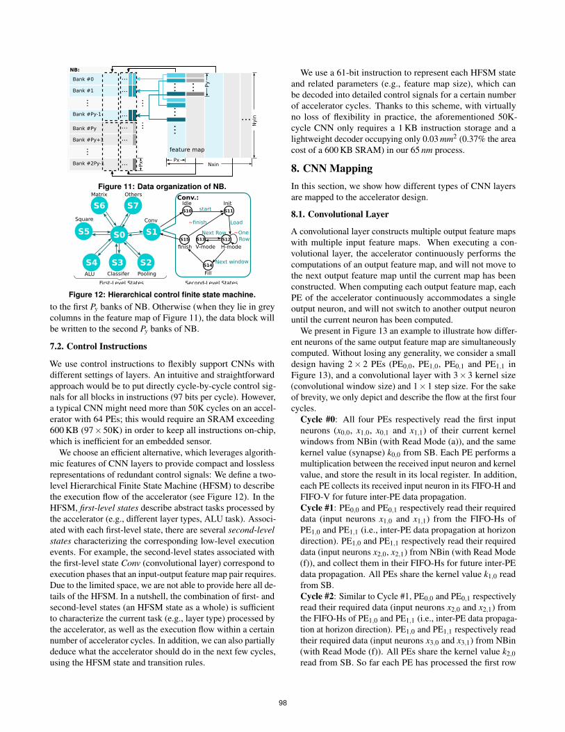
Figure 12: Hierarchical control finite state machine.
to the first Py banks of NB. Otherwise (when they lie in greycolumns in the feature map of Figure 11), the data block willbe written to the second Py banks of NB.
7.2. Control Instructions
We use control instructions to flexibly support CNNs withdifferent settings of layers. An intuitive and straightforwardapproach would be to put directly cycle-by-cycle control sig-nals for all blocks in instructions (97 bits per cycle). However,a typical CNN might need more than 50K cycles on an accel-erator with 64 PEs; this would require an SRAM exceeding600 KB (97×50K) in order to keep all instructions on-chip,which is inefficient for an embedded sensor.
We choose an efficient alternative, which leverages algorith-mic features of CNN layers to provide compact and losslessrepresentations of redundant control signals: We define a two-level Hierarchical Finite State Machine (HFSM) to describethe execution flow of the accelerator (see Figure 12). In theHFSM, first-level states describe abstract tasks processed bythe accelerator (e.g., different layer types, ALU task). Associ-ated with each first-level state, there are several second-levelstates characterizing the corresponding low-level executionevents. For example, the second-level states associated withthe first-level state Conv (convolutional layer) correspond toexecution phases that an input-output feature map pair requires.Due to the limited space, we are not able to provide here all de-tails of the HFSM. In a nutshell, the combination of first- andsecond-level states (an HFSM state as a whole) is sufficientto characterize the current task (e.g., layer type) processed bythe accelerator, as well as the execution flow within a certainnumber of accelerator cycles. In addition, we can also partiallydeduce what the accelerator should do in the next few cycles,using the HFSM state and transition rules.
We use a 61-bit instruction to represent each HFSM stateand related parameters (e.g., feature map size), which canbe decoded into detailed control signals for a certain numberof accelerator cycles. Thanks to this scheme, with virtuallyno loss of flexibility in practice, the aforementioned 50K-cycle CNN only requires a 1 KB instruction storage and alightweight decoder occupying only 0.03 mm2 (0.37% the areacost of a 600 KB SRAM) in our 65 nm process.
8. CNN MappingIn this section, we show how different types of CNN layersare mapped to the accelerator design.
8.1. Convolutional Layer
A convolutional layer constructs multiple output feature mapswith multiple input feature maps. When executing a con-volutional layer, the accelerator continuously performs thecomputations of an output feature map, and will not move tothe next output feature map until the current map has beenconstructed. When computing each output feature map, eachPE of the accelerator continuously accommodates a singleoutput neuron, and will not switch to another output neuronuntil the current neuron has been computed.
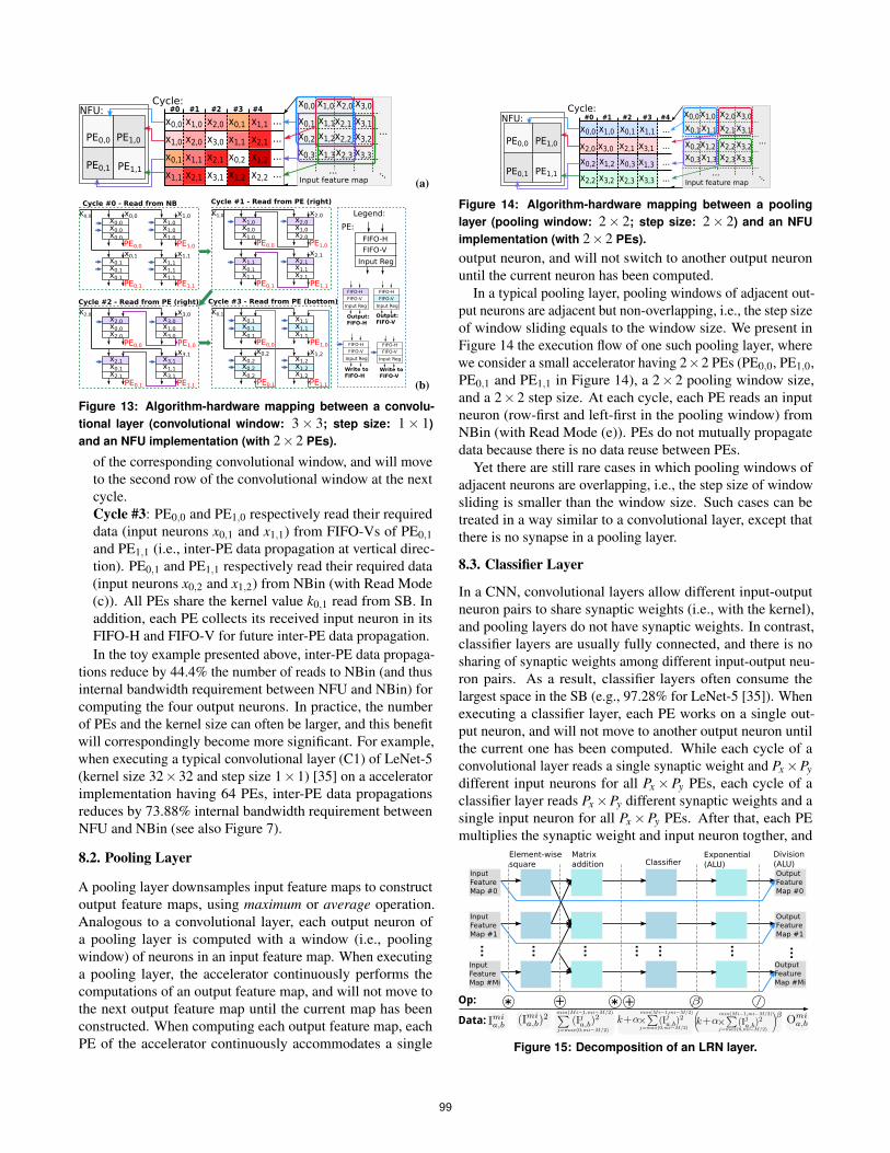
We present in Figure 13 an example to illustrate how differ-ent neurons of the same output feature map are simultaneouslycomputed. Without losing any generality, we consider a smalldesign having 2× 2 PEs (PE0,0, PE1,0, PE0,1 and PE1,1 inFigure 13), and a convolutional layer with 3× 3 kernel size(convolutional window size) and 1×1 step size. For the sakeof brevity, we only depict and describe the flow at the first fourcycles.
Cycle #0: All four PEs respectively read the first inputneurons (x0,0, x1,0, x0,1 and x1,1) of their current kernelwindows from NBin (with Read Mode (a)), and the samekernel value (synapse) k0,0 from SB. Each PE performs amultiplication between the received input neuron and kernelvalue, and store the result in its local register. In addition,each PE collects its received input neuron in its FIFO-H andFIFO-V for future inter-PE data propagation.Cycle #1: PE0,0 and PE0,1 respectively read their requireddata (input neurons x1,0 and x1,1) from the FIFO-Hs ofPE1,0 and PE1,1 (i.e., inter-PE data propagation at horizondirection). PE1,0 and PE1,1 respectively read their requireddata (input neurons x2,0, x2,1) from NBin (with Read Mode(f)), and collect them in their FIFO-Hs for future inter-PEdata propagation. All PEs share the kernel value k1,0 readfrom SB.Cycle #2: Similar to Cycle #1, PE0,0 and PE0,1 respectivelyread their required data (input neurons x2,0 and x2,1) fromthe FIFO-Hs of PE1,0 and PE1,1 (i.e., inter-PE data propaga-tion at horizon direction). PE1,0 and PE1,1 respectively readtheir required data (input neurons x3,0 and x3,1) from NBin(with Read Mode (f)). All PEs share the kernel value k2,0read from SB. So far each PE has processed the first row
98
x0,0 x1,0 x2,0 x0,1 x1,1
x1,0 x2,0 x3,0 x1,1 x2,1
x0,1 x1,1 x2,1 x0,2 x1,2
x1,1 x2,1 x3,1 x1,2 x2,2
...
...
...
...
NFU:
PE0,0 PE1,0
PE1,1PE0,1
Cycle: #0 #1 #2 #3 #4
...
... ...
x0,0 x1,0 x2,0 x3,0
x0,1 x1,1x2,1 x3,1
x0,2 x1,2x2,2 x3,2
x0,3 x1,3x2,3 x3,3
Input feature map (a)
K0,0
Cycle #0 - Read from NB
PE0,0
x0,0x0,0
x0,0x0,0
PE1,0
x1,0x1,0
x1,0x1,0
PE0,1
x0,1x0,1
x0,1x0,1
PE1,1
x1,1x1,1
x1,1x1,1
K1,0
x0,0x1,0
x1,0x1,0x2,0
x2,0x2,0
x0,1x1,1
x1,1x1,1x2,1
x2,1x2,1
Cycle #1 - Read from PE (right)
PE1,0PE0,0
PE0,1 PE1,1
K2,0
x0,0x2,0
x2,0x1,0x3,0
x3,0x3,0
x0,1x2,1
x2,1x1,1x3,1
x3,1x3,1
Cycle #2 - Read from PE (right)
PE1,0PE0,0
PE0,1 PE1,1
K0,1
x0,1x0,1
x0,1x1,1x1,1
x1,1
x0,2x0,2
x0,2x1,2x1,2
x1,2x1,2
x0,2
Cycle #3 - Read from PE (bottom)
PE1,0PE0,0
PE0,1 PE1,1
FIFO-H
FIFO-V
Input Reg
PE:
Output: FIFO-H
FIFO-H
FIFO-V
Input Reg
Output: FIFO-V
FIFO-H
FIFO-V
Input Reg
FIFO-H
FIFO-V
Input Reg
Write to FIFO-V
FIFO-H
FIFO-V
Input Reg
Legend:
Write to FIFO-H
(b)
Figure 13: Algorithm-hardware mapping between a convolu-tional layer (convolutional window: 3× 3; step size: 1× 1)and an NFU implementation (with 2×2 PEs).
of the corresponding convolutional window, and will moveto the second row of the convolutional window at the nextcycle.Cycle #3: PE0,0 and PE1,0 respectively read their requireddata (input neurons x0,1 and x1,1) from FIFO-Vs of PE0,1and PE1,1 (i.e., inter-PE data propagation at vertical direc-tion). PE0,1 and PE1,1 respectively read their required data(input neurons x0,2 and x1,2) from NBin (with Read Mode(c)). All PEs share the kernel value k0,1 read from SB. Inaddition, each PE collects its received input neuron in itsFIFO-H and FIFO-V for future inter-PE data propagation.In the toy example presented above, inter-PE data propaga-
tions reduce by 44.4% the number of reads to NBin (and thusinternal bandwidth requirement between NFU and NBin) forcomputing the four output neurons. In practice, the numberof PEs and the kernel size can often be larger, and this benefitwill correspondingly become more significant. For example,when executing a typical convolutional layer (C1) of LeNet-5(kernel size 32×32 and step size 1×1) [35] on a acceleratorimplementation having 64 PEs, inter-PE data propagationsreduces by 73.88% internal bandwidth requirement betweenNFU and NBin (see also Figure 7).
8.2. Pooling Layer
A pooling layer downsamples input feature maps to constructoutput feature maps, using maximum or average operation.Analogous to a convolutional layer, each output neuron ofa pooling layer is computed with a window (i.e., poolingwindow) of neurons in an input feature map. When executinga pooling layer, the accelerator continuously performs thecomputations of an output feature map, and will not move tothe next output feature map until the current map has beenconstructed. When computing each output feature map, eachPE of the accelerator continuously accommodates a single
x0,0 x1,0
x3,3
x0,1
x2,3
x2,0 x3,0
x1,1
x0,3 x1,3
x2,1
x0,2
x2,2 x3,2
x3,1
x1,2
...
...
...
...
NFU:
PE0,0 PE1,0
PE1,1PE0,1
Cycle: #0 #1 #2 #3 #4
...
......
x0,0x1,0 x2,0x3,0
x0,1x1,1 x2,1x3,1
x0,2x1,2 x2,2x3,2x0,3x1,3 x2,3x3,3
Input feature map
Figure 14: Algorithm-hardware mapping between a poolinglayer (pooling window: 2× 2; step size: 2× 2) and an NFUimplementation (with 2×2 PEs).
output neuron, and will not switch to another output neuronuntil the current neuron has been computed.
In a typical pooling layer, pooling windows of adjacent out-put neurons are adjacent but non-overlapping, i.e., the step sizeof window sliding equals to the window size. We present inFigure 14 the execution flow of one such pooling layer, wherewe consider a small accelerator having 2×2 PEs (PE0,0, PE1,0,PE0,1 and PE1,1 in Figure 14), a 2× 2 pooling window size,and a 2×2 step size. At each cycle, each PE reads an inputneuron (row-first and left-first in the pooling window) fromNBin (with Read Mode (e)). PEs do not mutually propagatedata because there is no data reuse between PEs.
Yet there are still rare cases in which pooling windows ofadjacent neurons are overlapping, i.e., the step size of windowsliding is smaller than the window size. Such cases can betreated in a way similar to a convolutional layer, except thatthere is no synapse in a pooling layer.
8.3. Classifier Layer
In a CNN, convolutional layers allow different input-outputneuron pairs to share synaptic weights (i.e., with the kernel),and pooling layers do not have synaptic weights. In contrast,classifier layers are usually fully connected, and there is nosharing of synaptic weights among different input-output neu-ron pairs. As a result, classifier layers often consume thelargest space in the SB (e.g., 97.28% for LeNet-5 [35]). Whenexecuting a classifier layer, each PE works on a single out-put neuron, and will not move to another output neuron untilthe current one has been computed. While each cycle of aconvolutional layer reads a single synaptic weight and Px×Pydifferent input neurons for all Px×Py PEs, each cycle of aclassifier layer reads Px×Py different synaptic weights and asingle input neuron for all Px×Py PEs. After that, each PEmultiplies the synaptic weight and input neuron togther, and
InputFeature Map #0
InputFeature Map #1
InputFeature Map #Mi
OutputFeature Map #0
OutputFeature Map #1
OutputFeature Map #Mi
+*Op:
Data:* +
ClassifierElement-wisesquare
Matrixaddition
Exponential(ALU)
Division (ALU)
...
...
...
...
...
...
...
Figure 15: Decomposition of an LRN layer.
99

...
...
...
...
...
InputFeature Map #0
InputFeature Map #1
InputFeature Map #Mi
OutputFeature Map #0
OutputFeature Map #1
OutputFeature Map #Mi
+* *-
...
* +Op:
Data:
Conv. Conv. Pooling/ClassifierMatrixaddition
Matrixaddtion
Element-wisesquare
Division (ALU)
Figure 16: Decomposition of an LCN layer.
accumulates the result to the partial sum stored at its local reg-ister. After a number of cycles, when the dot product (betweeninput neurons and synapses) associated with an output neuronhas been computed, the result will be sent to the ALU for thecomputation of activation function.
8.4. Normalization Layers
Normalization layers can be composed into a number of sub-layers and fundamental computational primitives in order to beexecuted by our accelerator. We illustrate detailed decomposi-tions in Figures 15 and 16, where an LRN layer is decomposedinto a classifier sub-layer, an element-wise square, a matrixaddition, exponential functions and divisions; and an LCNlayer is decomposed into two convolutional sub-layers, a pool-ing sub-layer, a classifier sub-layer, two matrix additions, anelement-wise square, and divisions. Convolutional, pooling,and classifier sub-layers can be tackled with the rules describedin former subsections, and exponential functions and divisionsare accommodated by the ALU. The rest computational primi-tives, including element-wise square and matrix addition, areaccommodated by the NFU. In supporting the two primitives,at each cycle, each PE works on an matrix element output withits multiplier or adder, and results of all Px×Py PEs are thenwritten to NBout, following the flow presented in Section 7.1.
9. Experimental Methodology
Measurements. We implemented our design in Verilog, syn-thesized it with Synopsys Design Compiler, and placed androuted it with Synopsys IC Compiler using the TSMC 65 nmGplus High VT library. We used CACTI 6.0 to estimate theenergy cost of DRAM accesses [42]. We compare our designwith three baselines:
CPU. The CPU baseline is a 256-bit SIMD (Intel XeonE7-8830, 2.13 GHz, 1 TB memory). We compile allbenchmarks with GCC 4.4.7 with options “-O3 -lm -march=native”, enabling the use of SIMD instructions suchas MMX, SSE, SSE2, SSE4.1 and SSE4.2.GPU. The GPU baseline is a modern GPU card (NVIDIAK20M, 5 GB GDDR5, 3.52 TFlops peak in 28 nm technol-ogy); we use the Caffe library, since it is widely regardedas the fastest CNN library for GPU [1].Accelerator. To make the comparison fair and adapted
Table 2: Benchmarks (C stands for a convolutional layer, S fora pooling layer, and F for a classifier layer).
Layer Kernel Size Layer Size Layer Kernel Size Layer Size#@size #@size #@size #@size
CN
P[4
6]
Input 1@42x42
MPC
NN
[43]
Input 1@32x32C1 6@7x7 6@36x36 C1 20@5x5 20@28x28S2 6@2x2 6@18x18 S2 20@2x2 20@14x14C3 61@7x7 16@12x12 C3 400@5x5 20@10x10S4 16@2x2 16@6x6 S4 20@2x2 20@5x5C5 305@6x6 80@1x1 C5 400@3x3 20@3x3F6 160@1x1 2@1x1 F6 6000@1x1 300@1x1
F7 1800@1x1 6@1x1
Layer Kernel Size Layer Size Layer Kernel Size Layer Size#@size #@size #@size #@size
Face
Rec
og.[
33] Input 1@23x28
LeN
et-5
[35]
Input 1@32x32C1 20@3x3 20@21x26 C1 6@5x5 6@28x28S2 20@2x2 20@11x13 S2 6@2x2 6@14x14C3 125@3x3 25@9x11 C3 60@5x5 16@10x10S4 25@2x2 25@5x6 S4 16@2x2 16@5x5F5 1000@1x1 40@1x1 F5 1920@5x5 120@1x1
F6 10080@1x1 84@1x1F7 840@1x1 10@1x1
Layer Kernel Size Layer Size Layer Kernel Size Layer Size#@size #@size #@size #@size
Sim
ple
Con
v[5
3]Input 1@29x29
CFF
[17]
Input 1@32x36C1 5@5x5 5@13x13 C1 4@5x5 4@28x32C2 250@5x5 50@5x5 S2 4@2x2 4@14x16F3 5000@1x1 100@1x1 C3 20@3x3 14@12x14F4 1000@1x1 10@1x1 S4 14@2x2 14@6x7
F5 14@6x7 14@1x1F6 14@1x1 1@1x1
Layer Kernel Size Layer Size Layer Kernel Size Layer Size#@size #@size #@size #@size
NE
O[4
4]
Input 1@24x24
Con
vNN
[9]
Input 3@64x36C1 4@5x5 1@24x24 C1 12@5x5 12@60x32S2 6@3x3 4@12x12 S2 12@2x2 12@30x16C3 14@5x5 4@12x12 C3 60@3x3 14@28x14S4 60@3x3 16@6x6 S4 14@2x2 14@14x7F5 160@6x7 10@1x1 F5 14@14x7 14@1x1
F6 14@1x1 1@1x1
Layer Kernel Size Layer Size Layer Kernel Size Layer Size#@size #@size #@size #@size
Gab
or[3
0]
Input 1@20x20
Face
Alig
n.[1
1]
Input 1@46x56C1 4@5x5 4@16x16 C1 4@7x7 4@40x50S2 4@2x2 4@8x8 S2 4@2x2 4@20x25C3 20@3x3 14@6x6 C3 6@5x5 3@16x21S4 14@2x2 14@3x3 S4 3@2x2 3@8x10F5 14@1x1 14@1x1 F5 180@8x10 60@1x1F6 14@1x1 1@1x1 F6 240@1x1 4@1x1
to the embedded scenario, we resized our previous work,i.e., DianNao [3] to have a comparable amount of arith-metic operators as our design—i.e., we implemented an8×8 DianNao-NFU (8 hardware neurons, each processes 8input neurons and 8 synapses per cycle) with a 62.5 GB/sbandwidth memory model instead of the original 16×16DianNao-NFU with 250 GB/s bandwidth memory model(unrealistic in a vision sensor). We correspondingly shrankthe sizes of on-chip buffers by half in our re-implementationof DianNao: 1 KB NBin/NBout and 16 KB SB. We haveverified that our implementation is roughly fitting to the orig-inal design. For instance, we obtained an area of 1.38 mm2
for our re-implementation versus 3.02 mm2 for the originalDianNao [3], which tracks well the ratio in computing andstorage resources.
100

NBin
NBout
SB
IB
NFU
Figure 17: Layout of ShiDianNao (65 nm).
Benchmarks. We collected 10 CNNs from representativevisual recognition applications and used them as our bench-marks (Table 2). Among all layers of all benchmarks, inputneurons consume at most 45 KB, and synapses consume atmost 118 KB, which do not exceed the SRAM capacities ofour design (Table 3).
10. Experimental Results
10.1. Layout Characteristics
We present in Tables 3 and 4 the parameters and layout char-acteristics of the current ShiDianNao version (see Figure 17),respectively. ShiDianNao has 8× 8 (64) PEs and a 64 KBNBin, a 64 KB NBout, a 128 KB SB, and a 32 KB IB. Theoverall SRAM capacity of ShiDianNao is 288 KB (11.1×larger than that of DianNao), in order to simultaneously storeall data and instructions for a practical CNN. Yet, the totalarea of ShiDianNao is only 3.52× larger than that of DianNao(4.86 mm2 vs. 1.38 mm2).
10.2. Performance
We compare ShiDianNao against the CPU, the GPU, and Di-anNao on all benchmarks listed in Section 9. The results areshown in Figure 18. Unsurprisingly, ShiDianNao significantlyoutperforms the general purpose architectures and is, on aver-age, 46.38 × faster than the CPU and 28.94× faster than theGPU. In particular, the GPU cannot take full advantage of itshigh computational power because the small computationalkernels of the visual recognition tasks listed in Table 1 mappoorly on its 2,496 hardware threads.
More interestingly, ShiDianNao also outperforms our accel-erator baseline on 9 out of 10 benchmarks (1.87× faster onaverage on all 10 benchmarks). There are two main reasons forthat: Firstly, compared to DianNao, ShiDianNao eliminatesoff-chip memory accesses during execution, thanks to a suffi-ciently large SRAM capacity and a correspondingly slightlyhigher cost. Secondly, ShiDianNao efficiently exploits the lo-cality of 2D feature maps with its dedicated SRAM controllersand its inter-PE data reuse mechanism; DianNao, on the otherhand, cannot make good use of that locality.
ShiDianNao performs slightly worse than the acceleratorbaseline on benchmark Simple Conv. The issue is that ShiD-ianNao works on a single output feature map at a time andeach PE works on a single output neuron of the feature map.
Table 3: Parameter settings of ShiDianNao and DianNao.
ShiDianNao DianNao
Data width 16-bit 16-bit# multipliers 64 64NBin SRAM size 64 KB 1 KBNBout SRAM size 64 KB 1 KBSB SRAM size 128 KB 16 KBInst. SRAM size 32 KB 8 KB
Table 4: Hardware characteristics of ShiDianNao at 1GHz,where power and energy are averaged over 10 benchmarks.
Accelerator Area (mm2) Power (mW ) Energy (nJ)
Total 4.86 (100%) 320.10 (100%) 6048.70 (100%)NFU 0.66 (13.58%) 268.82 (83.98%) 5281.09 (87.29%)NBin 1.12 (23.05%) 35.53 (11.10%) 475.01 (7.85%)NBout 1.12 (23.05%) 6.60 (2.06%) 86.61 (1.43%)SB 1.65 (33.95%) 6.77 (2.11%) 94.08 (1.56%)IB 0.31 (6.38%) 2.38 (0.74%) 35.84 (0.59%)
Therefore, when most of an application consists of uncom-monly small output feature maps with fewer output neuronsthan implemented PEs (e.g., 5× 5 in the C2 layer of bench-mark Simple Conv for 8× 8 PEs in the current acceleratordesign), some PEs will be idle. Although we played with theidea of alleviating this issue by adding complicated controllogic to each PE and allowing different PEs to simultaneouslywork on different feature maps, we ultimately decided againstthis option as it appeared a poor trade-off with a detrimentalimpact on the programming model.
Concerning the ability of ShiDianNao to process in realtime a stream of frames from a sensor, the longest time toprocess a 640x480 video frame is for benchmark ConvNNwhich requires 0.047 ms to process a 64× 36-pixel region.Since each frame contains d(640− 64)/16 + 1e × d(480−36)/16+1e= 1073 such regions (overlapped by 16 pixels),a frame takes a little more than 50 ms to process, resultingin a speed of 20 frames per second for the most demandingbenchmark. Since typical commercial sensors can streamdata at a desired rate and since streaming speed can thus bematched to the processing rate, the partial frame buffer muststore only the parts of the image reused across overlappingregions. This is of the order of a few tens of pixel rows and fitswell the 256 KB of commercial image processors. Althoughapparently low, the 640×480 resolution is in line with thefact that usually images are resized in certain range beforeprocessing [47, 34, 23, 16].
10.3. Energy
In Figure 19, we report the energy consumed by GPU, Dian-Nao and ShiDianNao, inclusive of main memory accesses toobtain the input data. Even if ShiDianNao is not meant toaccess DRAM, we have conservatively included main mem-ory accesses for the sake of a fair comparison. ShiDianNaois on average 4688.13× and 63.48× more energy efficientthan GPU and DianNao, respectively. We also evaluate anideal version of DianNao (DianNao-FreeMem, see Figure 19),where we assume that main memory accesses incur no en-ergy cost. Interestingly, we observe that ShiDianNao is still
101

Spe
edup
(vs
. CP
U)
020
4060
8010
0
CPUGPUDianNaoShiDianNao
CNPMPCNN
Face Reco.
Lenet−5
Simple Conv
CFFNEO
ConvNN
Gabor
Face align.
GeoMean
Figure 18: Speedup of GPU, DianNao, and ShiDianNao overthe CPU.
log(
Ene
rgy)
(nJ
)
34
56
78 GPU DianNao DianNao−FreeMem ShiDianNao
CNPMPCNN
Face Reco.
Lenet−5
Simple Conv
CFFNEO
ConvNN
Gabor
Face align.
GeoMean
Figure 19: Energy cost of GPU, DianNao, and ShiDianNao.
1.66× more energy efficient than DianNao-FreeMem. More-over, when ShiDianNao is integrated in an embedded visionsensor and frames are stored directly into its NBin, the superi-ority is even more significant: in this setting, ShiDianNao is87.39× and 2.37× more energy efficient than DianNao andDianNao-FreeMem, respectively.
We illustrate in Table 4 the breakdown of the energy con-sumed by our design. We observe that four SRAM buffersaccount for only 11.43% the overall energy, and the rest isconsumed by the logic (87.29%). This is significantly differentfrom Chen et al.’s observation made on DianNao [3], wheremore than 95% of the energy is consumed by the DRAM.
11. Related Work
Visual sensor and processing. Due to the rapid developmentof integrated circuits and sensor technologies, the size andcost of a vision sensor quickly scales down, which offers agreat opportunity to integrate higher-resolution sensors in mo-bile ends and wearable devices (e.g., Google Glass [54] andSamsung Gear [49]). Under emerging application scenariossuch as image recognition/search [19, 54], however, end de-vices do not locally perform intensive visual processing onimages captured by sensors, due to the limited computationalcapacity and power budget. Instead, computation-intensivevisual processing algorithms like CNNs [27, 17, 33, 30] are
performed at the sever end, leading to considerable workloadsto the server, which greatly limits the QoS and, ultimately, thegrowth of end users. Our study partially bridges this gap byshifting visual processing closer to sensors.
Neural network accelerators. Neural networks were con-ventionally executed on CPUs [59, 2], and GPUs [15, 51, 5].These platforms can flexibly adapt to various workloads, butthe flexibility is achieved at a large fraction of transistors, sig-nificantly affecting the energy-efficiency of executing specificworkloads such as CNNs (see Section 3). After a first waveof designs at the end of the last century [25], there have alsobeen a few more modern application-specific accelerator ar-chitectures for various neural networks, with implementationson either FPGAs [50, 46, 52] or ASICs [3, 16, 57]. For CNNs,Farabet et al. proposed a systolic architecture called NeuFlowarchitecture [16], Chakradhar et al. designed a systolic-likecoprocessor [2]. Although effective to handle 2D convolutionin signal processing [37, 58, 38, 22], systolic architectures donot provide sufficient flexibility and efficiency to support dif-ferent settings of CNNs [8, 50, 16, 2], which is exemplified bytheir strict restrictions on CNN parameters (e.g., size of con-volutional window, step size of window sliding, etc), as wellas their high memory bandwidth requirements. There havebeen some neural network accelerators adopting SIMD-likearchitectures. Esmaeilzadeh et al. proposed a neural networkstream processing core (NnSP) with an array of PEs, but thereleased version is still designed for Multi-Layer Perceptrons(MLPs) [12]. Peemen et al. [45] proposed to accelerate CNNswith an FPGA accelerator controlled by a host processor. Al-though this accelerator is equipped with a memory subsystemcustomized for CNNs, the requirement of a host processor lim-its the overall energy efficiency. Gokhale et al. [18] designeda mobile coprocessor for visual processing at mobile devices,which supports both CNNs and DNNs. The above studies didnot treat main memory accesses as the first-order concern, ordirectly linked the computational block to the main memoryvia a DMA. Recently, some of us [3] designed dedicated on-chip SRAM buffers to reduce main memory accesses, and theproposed DianNao accelerator cover a broad range of neuralnetworks including CNNs. However, in order to flexibly sup-port different neural networks, DianNao does not implementspecialized hardware to exploit data locality of 2D featuremaps in a CNN, but instead treats them as 1D data vectors incommon MLPs. Therefore, DianNao still needs frequent mem-ory accesses to execute a CNN, which is less energy efficientthan our design (see Section 10 for experimental comparisons).Recent members of the DianNao family [4, 40] have been op-timized for large-scale neural networks and classic machinelearning techniques respectively. However, they are not de-signed for embedded applications, and their architectures aresignificantly different from the ShiDianNao architecture.
Our design is substantially different from previous studiesin two aspects. First, unlike previous designs requiring mem-ory accesses to get data, our design does not access to the main
102
memory when executing a CNN. Second, unlike previous sys-tolic designs supporting a single CNN with a fixed parameterand layer setting [2, 8, 16, 50], or a single convolutional layerwith fixed parameters, our design flexibly accommodates dif-ferent CNNs with different parameter and layer settings. Dueto these attractive features, our design is more energy-efficientthan previous designs on CNNs, thus particularly suits visualrecognition in embedded systems.
12. Conclusions
We designed a versatile accelerator for state-of-the-art visualrecognition algorithms. Averaged on 10 representative bench-marks, our design is, respectively, about 50×, 30×, and 1.87×faster than a mainstream CPU, a GPU, and our own reim-plementation of the DianNao neural network accelerator [3].ShiDianNao consumes only about 4700x and 60x less energythan the GPU and DianNao, respectively. Our design hasan area of 4.86 mm2 in a 65 nm process and consumes only320.10 mW at 1 GHz. Thanks to its high performance, its lowpower consumption, as well as its small area, ShiDianNaoparticularly suits visual applications at mobile ends and wear-able devices. Our accelerator is suitable for integration in suchdevices, on the streaming path from sensors to hosts. Thiswould significantly reduce workloads at servers, greatly en-hance the QoS of emerging visual applications, and eventuallycontribute to the ubiquitous success of visual processing.
Acknowledgments
This work is partially supported by the NSF of China (underGrants 61100163, 61133004, 61222204, 61221062, 61303158,61432016, 61472396, 61473275, 60921002), the 973 Pro-gram of China (under Grant 2015CB358800, 2011CB302504),the Strategic Priority Research Program of the CAS (un-der Grants XDA06010403, XDB02040009), the Interna-tional Collaboration Key Program of the CAS (under Grant171111KYSB20130002), and the 10000 talent program.
References[1] Berkeley Vision and Learning Center, “Caffe: a deep learning
framework.” Available: http://caffe.berkeleyvision.org/[2] S. Chakradhar, M. Sankaradas, V. Jakkula, and S. Cadambi,
“A dynamically configurable coprocessor for convolutional neuralnetworks,” in Proceedings of the 37th annual international symposiumon Computer architecture (ISCA). New York, USA: ACM Press,2010, pp. 247–257.
[3] T. Chen, Z. Du, N. Sun, J. Wang, and C. Wu, “DianNao: asmall-footprint high-throughput accelerator for ubiquitous machine-learning,” in Proceedings of the 19th International Conference onArchitectural Support for Programming Languages and OperatingSystems (ASPLOS), Salt Lake City, UT, USA, 2014, pp. 269–284.
[4] Y. Chen, T. Luo, S. Liu, S. Zhang, L. He, J. Wang, L. Li, T. Chen, Z. Xu,N. Sun, and O. Temam, “DaDianNao: A Machine-Learning Supercom-puter,” in Proceedings of the 47th Annual IEEE/ACM InternationalSymposium on Microarchitecture (MICRO), 2015, pp. 609–622.
[5] D. C. Cires, U. Meier, J. Masci, and L. M. Gambardella, “Flexible, High Performance Convolutional Neural Networks for Image Clas-sification,” in Proceedings of the Twenty-Second International JointConference on Artificial Intelligence (IJCNN), 2003, pp. 1237–1242.
[6] A. Coates, B. Huval, T. Wang, D. J. Wu, and A. Y. Ng, “Deep learningwith COTS HPC systems,” in Proceedings of the 30th InternationalConference on Machine Learning (ICML), 2013, pp. 1337–1345.
[7] G. Dahl, T. Sainath, and G. Hinton, “Improving deep neural networksfor LVCSR using rectified linear units and dropout,” in IEEEInternational Conference on Acoustics, Speech and Signal Processing(ICASSP’13), 2013, pp. 8609–8613.
[8] S. A. Dawwd, “The multi 2D systolic design and implementation ofConvolutional Neural Networks,” in 2013 IEEE 20th InternationalConference on Electronics, Circuits, and Systems (ICECS). IEEE,Dec. 2013, pp. 221–224.
[9] M. Delakis and C. Garcia, “Text Detection with Convolutional NeuralNetworks,” in International Conference on Computer Vision Theoryand Applications (VISAPP), 2008, pp. 290–294.
[10] Z. Du, A. Lingamneni, Y. Chen, K. Palem, O. Temam, and C. Wu,“Leveraging the error resilience of machine-learning applicationsfor designing highly energy efficient accelerators,” 2014 19th Asiaand South Pacific Design Automation Conference (ASP-DAC), pp.201–206, Jan. 2014.
[11] S. Duffner and C. Garcia, “Robust Face Alignment Using Convolu-tional Neural Networks,” in International Conference on ComputerVision Theory and Applications (VISAPP), 2008, pp. 30–37.
[12] H. Esmaeilzadeh, P. Saeedi, B. Araabi, C. Lucas, and S. Fakhraie,“Neural Network Stream Processing Core (NnSP) for EmbeddedSystems,” 2006 IEEE International Symposium on Circuits andSystems (ISCS), pp. 2773–2776, 2006.
[13] H. Esmaeilzadeh, A. Sampson, L. Ceze, and D. Burger, “NeuralAcceleration for General-Purpose Approximate Programs,” 2012 45thAnnual IEEE/ACM International Symposium on Microarchitecture(MICRO), pp. 449–460, Dec. 2012.
[14] K. Fan, S. Mahlke, and A. Arbor, “Bridging the Computation GapBetween Programmable Processors and Hardwired Accelerators,” inIEEE 15th International Symposium on High Performance ComputerArchitecture (HPCA), 2009, pp. 313–322.
[15] C. Farabet, B. Martini, P. Akselrod, S. Talay, Y. LeCun, andE. Culurciello, “Hardware accelerated convolutional neural networksfor synthetic vision systems,” in Proceedings of 2010 IEEEInternational Symposium on Circuits and Systems (ISCS). IEEE,May 2010, pp. 257–260.
[16] C. Farabet, B. Martini, B. Corda, P. Akselrod, E. Culurciello, andY. LeCun, “NeuFlow: A runtime reconfigurable dataflow processor forvision,” in IEEE Computer Society Conference on Computer Visionand Pattern Recognition Workshops (CVPRW). IEEE, Jun. 2011, pp.109–116.
[17] C. Garcia and M. Delakis, “Convolutional face finder: a neuralarchitecture for fast and robust face detection.” IEEE Transactions onPattern Analysis and Machine Intelligence (PAMI), vol. 26, no. 11, pp.1408–23, Nov. 2004.
[18] V. Gokhale, J. Jin, and A. Dundar, “A 240 G-ops/s mobile coprocessorfor deep neural networks,” in Proceedings of the IEEE Conference onComputer Vision and Pattern Recognition Workshops (CVPRW), 2014,pp. 682–687.
[19] Google, “Google image search.” Available: http://www.google.com/insidesearch/features/images/searchbyimage.htm
[20] R. Hameed, W. Qadeer, M. Wachs, O. Azizi, A. Solomatnikov, B. C.Lee, S. Richardson, C. Kozyrakis, and M. Horowitz, “Understandingsources of inefficiency in general-purpose chips,” in Proceedings ofAnnual International Symposium on Computer Architecture (ISCA).New York, USA: ACM Press, 2010, p. 37.
[21] S. Haykin, Neural Networks: A Comprehensive Foundation, 2nd ed.Upper Saddle River, NJ, USA: Prentice Hall PTR, 1998.
[22] V. Hecht, K. Ronner, and P. Pirsch, “An Advanced Programmable2D-Convolution Chip for Real Time Image Processing,” in IEEE Inter-national Sympoisum on Circuits and Systems (ISCS), 1991, pp. 1897 –1900.
[23] G. E. Hinton, N. Srivastava, A. Krizhevsky, I. Sutskever, andR. R. Salakhutdinov, “Improving neural networks by preventing co-adaptation of feature detectors,” in arXiv: 1207.0580 (2012), pp. 1–18.
[24] P. S. Huang, X. He, J. Gao, and L. Deng, “Learning deepstructured semantic models for web search using clickthrough data,” inInternational Conference on Information and Knowledge Management(CIKM), 2013, pp. 2333–2338.
[25] P. Ienne, T. Cornu, and G. Kuhn, “Special-purpose digital hardwarefor neural networks: An architectural survey,” Journal of VLSI SignalProcessing, vol. 13, no. 1, pp. 5–25, 1996.
103

[26] K. Jarrett, K. Kavukcuoglu, M. A. Ranzato, and Y. LeCun, “Whatis the best multi-stage architecture for object recognition?” 2009IEEE 12th International Conference on Computer Vision (ICCV), pp.2146–2153, Sep. 2009.
[27] S. Kamijo, Y. Matsushita, K. Ikeuchi, and M. Sakauchi, “Trafficmonitoring and accident detection at intersections,” IEEE Transactionson Intelligent Transportation Systems, vol. 1, no. 2, pp. 108–118, Jun.2000.
[28] S. W. Keckler, W. J. Dally, B. Khailany, M. Garland, and D. Glasco,“GPUs and the future of parallel computing,” IEEE Micro, pp. 7–17,2011.
[29] A. Krizhevsky, I. Sutskever, and G. E. Hinton, “ImageNet Classifica-tion with Deep Convolutional Neural Networks,” Advances In NeuralInformation Processing Systems, pp. 1–9, 2012.
[30] B. Kwolek, “Face detection using convolutional neural networks andGabor filters,” Artificial Neural Networks: Biological Inspirations(ICANN), pp. 551–556, 2005.
[31] D. Larkin, A. Kinane, V. Muresan, and N. E. O’Connor, “An Effi-cient Hardware Architecture for a Neural Network Activation FunctionGenerator,” in Advances in Neural Networks, ser. Lecture Notes inComputer Science, vol. 3973. Springer, 2006, pp. 1319–1327.
[32] H. Larochelle, D. Erhan, A. Courville, J. Bergstra, and Y. Bengio,“An empirical evaluation of deep architectures on problems withmany factors of variation,” in International Conference on MachineLearning (ICML). New York, New York, USA: ACM Press, 2007,pp. 473–480.
[33] S. Lawrence, C. L. Giles, a. C. Tsoi, and a. D. Back, “Face recognition:a convolutional neural-network approach.” IEEE Transactions onNeural Networks, vol. 8, no. 1, pp. 98–113, Jan. 1997.
[34] Q. V. Le, M. A. Ranzato, M. Devin, G. S. Corrado, and A. Y. Ng,“Building High-level Features Using Large Scale Unsupervised Learn-ing,” International Conference on Machine Learning (ICML), pp. 8595– 8598, 2012.
[35] Y. LeCun, L. Bottou, Y. Bengio, and P. Haffner, “Gradient-BasedLearning Applied to Document Recognition,” Proceedings of the IEEE,vol. 86, no. 11, pp. 2278– 2324, 1998.
[36] Y. LeCun, K. Kavukcuoglu, and C. Farabet, “Convolutional networksand applications in vision,” Proceedings of 2010 IEEE InternationalSymposium on Circuits and Systems (ISCS), pp. 253–256, May 2010.
[37] J.-J. Lee and G.-Y. Song, “Super-Systolic Array for 2D Convolution,”2006 IEEE Region 10 Conference (TENCON), pp. 1–4, 2006.
[38] S. Y. Lee and J. K. Aggarwal, “Parallel 2D convolution on a MeshConnected Array Processor,” IEEE Transactions on Pattern Analysisand Machine Intelligence (PAMI), vol. PAMI-9, no. 4, pp. 590–594,1987.
[39] B. Liang and P. Dubey, “Recognition, Mining and Synthesis,” IntelTechnology Journal, vol. 09, no. 02, 2005.
[40] D. Liu, T. Chen, S. Liu, J. Zhou, S. Zhou, O. Temam, X. Feng,X. Zhou, and Y. Chen, “Pudiannao: A polyvalent machine learningaccelerator,” in Proceedings of the Twentieth International Conferenceon Architectural Support for Programming Languages and OperatingSystems (ASPLOS ), 2015, pp. 369–381.
[41] V. Mnih and G. Hinton, “Learning to Label Aerial Images from NoisyData,” in Proceedings of the 29th International Conference on MachineLearning (ICML), 2012, pp. 567–574.
[42] N. Muralimanohar, R. Balasubramonian, and N. Jouppi, “OptimizingNUCA Organizations and Wiring Alternatives for Large Caches withCACTI 6.0,” The 40th Annual IEEE/ACM International Symposium onMicroarchitecture (MICRO), pp. 3–14, Dec. 2007.
[43] J. Nagi, F. Ducatelle, G. A. D. Caro, D. Cires, U. Meier, A. Giusti, andL. M. Gambardella, “Max-Pooling Convolutional Neural Networksfor Vision-based Hand Gesture Recognition,” in IEEE InternationalConference on Signal and Image Processing Applications (ICSIPA),2011, pp. 342–347.
[44] C. Nebauer, “Evaluation of convolutional neural networks for visualrecognition.” IEEE Transactions on Neural Networks, vol. 9, no. 4, pp.685–96, Jan. 1998.
[45] M. Peemen, A. a. a. Setio, B. Mesman, and H. Corporaal, “Memory-centric accelerator design for Convolutional Neural Networks,” inInternational Conference on Computer Design (ICCD). IEEE, Oct.2013, pp. 13–19.
[46] C. Poulet, J. Y. Han, and Y. Lecun, “CNP: An FPGA-based processorfor Convolutional Networks,” in International Conference on FieldProgrammable Logic and Applications (FPL), vol. 1, no. 1, 2009, pp.32–37.
[47] M. Ranzato, F. J. Huang, Y. L. Boureau, and Y. LeCun, “Unsupervisedlearning of invariant feature hierarchies with applications to objectrecognition,” in Computer Vision and Pattern Recognition (CVPR).IEEE, Jun. 2007, pp. 1–8.
[48] R. Salakhutdinov and G. Hinton, “Learning a nonlinear embedding bypreserving class neighbourhood structure,” in AI and Statistics, ser.JMLR Workshop and Conference Proceedings, vol. 3, no. 5. Citeseer,2007, pp. 412–419.
[49] SAMSUNG, “SAMSUNG Gear2 Tech Specs,” Samsung Electronics,2014.
[50] M. Sankaradas, V. Jakkula, S. Cadambi, S. Chakradhar, I. Durdanovic,E. Cosatto, and H. P. Graf, “A Massively Parallel Coprocessorfor Convolutional Neural Networks,” 2009 20th IEEE InternationalConference on Application-specific Systems, Architectures andProcessors (ASAP), pp. 53–60, Jul. 2009.
[51] D. Scherer, H. Schulz, and S. Behnke, “Accelerating large-scaleconvolutional neural networks with parallel graphics multiprocessors,”in Artificial Neural Networks (ICANN), ser. Lecture Notes in ComputerScience, K. Diamantaras, W. Duch, and L. Iliadis, Eds. SpringerBerlin Heidelberg, 2010, vol. 6354, pp. 82–91.
[52] P. Sermanet and Y. LeCun, “Traffic sign recognition with multi-scaleConvolutional Networks,” in International Joint Conference on NeuralNetworks (IJCNN). Ieee, Jul. 2011, pp. 2809–2813.
[53] P. Y. Simard, D. Steinkraus, and J. C. Platt, “Best practices forconvolutional neural networks applied to visual document analysis,”in Seventh International Conference on Document Analysis andRecognition 2003 Proceedings (ICDAR), vol. 1. IEEE Comput. Soc,2003, pp. 958–963.
[54] T. Starner, “Project Glass: An Extension of the Self,” IEEE PervasiveComputing, vol. 12, no. 2, pp. 14–16, Apr. 2013.
[55] STV0986, 5 Megapixel mobile imaging processor (Data Brief), STMi-croelectronics, Jan. 2007.
[56] STV0987, 8 Megapixel mobile imaging processor (Data Brief), STMi-croelectronics, Mar. 2013.
[57] O. Temam, “A defect-tolerant accelerator for emerging high-performance applications,” 2012 39th Annual International Symposiumon Computer Architecture (ISCA), vol. 00, no. c, pp. 356–367, 2012.
[58] H. Tkung and D. Wl, “Two-level pipelined systolic array for multidi-mensional convolution,” Image and Vision Computing, vol. 1, no. 1,pp. 30–36, 1983.
[59] V. Vanhoucke, A. Senior, and M. Z. Mao, “Improving the speed of neu-ral networks on CPUs,” in Deep Learning and Unsupervised FeatureLearning Workshop, Neural Information Processing Systems Confer-ence (NIPS), 2011.
[60] G. Venkatesh, J. Sampson, N. Goulding-hotta, S. K. Venkata, M. B. Tay-lor, and S. Swanson, “QSCORES : Trading Dark Silicon for ScalableEnergy Efficiency with Quasi-Specific Cores Categories and SubjectDescriptors,” in Proceedings of the 44th Annual IEEE/ACM Interna-tional Symposium on Microarchitecture (MICRO), 2011, pp. 163–174.
[61] S. Yehia, S. Girbal, H. Berry, and O. Temam, “Reconciling special-ization and flexibility through compound circuits,” in IEEE 15th In-ternational Symposium on High Performance Computer Architecture(HPCA). IEEE, 2009, pp. 277–288.
104