IS49FL004T - · PDF fileis49fl004t integrated silicon solution, inc.- rev. c 2/1/2013 3 f wh f...
55
IS49FL004T Integrated Silicon Solution, Inc.- www.issi.com Rev. C 2/1/2013 1 2 Mbit / 4 Mbit 3.3 Volt-only Firmware Hub/LPC Flash Memory FEATURES • Single Power Supply Operation - Low voltage range: 3.0 V - 3.6 V • Standard Intel Firmware Hub/LPC Interface - Read compatible to Intel ® 82802 Firmware Hub devices - Conforms to Intel LPC Interface Specification Revision 1.1 • Memory Configuration - IS49FL002: 256K x 8 (2 Mbit) - IS49FL004: 512K x 8 (4 Mbit) • Cost Effective Sector/Block Architecture - IS49FL002: Sixty-four uniform 4 Kbyte sectors, or sixteen uniform 16 Kbyte blocks (sector group) - IS49FL004: One hundred and twenty-eight uniform 4 Kbyte sectors, or eight uniform 64 Kbyte blocks (sector group) • Top Boot Block - IS49FL002: 16 Kbyte top Boot Block - IS49FL004: 64 Kbyte top Boot Block • Automatic Erase and Program Operation - Build-in automatic program verification for extended product endurance - Typical 25 μs/byte programming time - Typical 50 ms sector/block/chip erase time • Two Configurable Interfaces - In-System hardware interface: Auto detection of Firmware Hub (FWH) or Low Pin Count (LPC) memory cycle for in-system read and write operations - Address/Address-Multiplexed (A/A Mux) interface for programming on EPROM Pro- grammers during manufacturing • Firmware HUB (FWH)/Low Pin Count (LPC) Mode - 33 MHz synchronous operation with PCI bus - 5-signal communication interface for in-system read and write operations - Standard SDP Command Set - Data# Polling and Toggle Bit features - Register-based read and write protection for each block (FWH mode only) - 4 ID pins for multiple Flash chips selection (FWH mode only) - 5 GPI pins for General Purpose Input Register - TBL# pin for hardware write protection to Boot Block - WP# pin for hardware write protection to whole memory array except Boot Block • Address/Address Multiplexed (A/A Mux) Mode - 11-pin multiplexed address and 8-pin data I/O interface - Supports fast programming on EPROM programmers - Standard SDP Command Set - Data# Polling and Toggle Bit features • Lower Power Consumption - Typical 2 mA active read current - Typical 7 mA program/erase current • High Product Endurance - Guarantee 100,000 program/erase cycles per single sector (preliminary) - Minimum 20 years data retention • Compatible Pin-out and Packaging - 32-pin (8 mm x 14 mm) VSOP - 32-pin PLCC - Optional Halogen-free package • Hardware Data Protection
Transcript of IS49FL004T - · PDF fileis49fl004t integrated silicon solution, inc.- rev. c 2/1/2013 3 f wh f...

IS49FL004T
Integrated Silicon Solution, Inc.- www.issi.com
Rev. C
2/1/2013
1
2 Mbit / 4 Mbit 3.3 Volt-only Firmware Hub/LPC Flash Memory
FEATURES
• Single Power Supply Operation
- Low voltage range: 3.0 V - 3.6 V
• Standard Intel Firmware Hub/LPC Interface
- Read compatible to Intel® 82802 Firmware Hub
devices
- Conforms to Intel LPC Interface Specification
Revision 1.1
• Memory Configuration
- IS49FL002: 256K x 8 (2 Mbit)
- IS49FL004: 512K x 8 (4 Mbit)
• Cost Effective Sector/Block Architecture
- IS49FL002: Sixty-four uniform 4 Kbyte
sectors, or sixteen uniform 16 Kbyte blocks
(sector group)
- IS49FL004: One hundred and twenty-eight
uniform 4 Kbyte sectors, or eight uniform 64
Kbyte blocks (sector group)
• Top Boot Block
- IS49FL002: 16 Kbyte top Boot Block
- IS49FL004: 64 Kbyte top Boot Block
• Automatic Erase and Program Operation
- Build-in automatic program verification for
extended product endurance
- Typical 25 µs/byte programming time
- Typical 50 ms sector/block/chip erase time
• Two Configurable Interfaces
- In-System hardware interface: Auto detection of
Firmware Hub (FWH) or Low Pin Count (LPC)
memory cycle for in-system read and write
operations
- Address/Address-Multiplexed (A/A Mux)
interface for programming on EPROM Pro-
grammers during manufacturing
• Firmware HUB (FWH)/Low Pin Count (LPC)
Mode
- 33 MHz synchronous operation with PCI bus
- 5-signal communication interface for in-system
read and write operations
- Standard SDP Command Set
- Data# Polling and Toggle Bit features
- Register-based read and write protection for
each block (FWH mode only)
- 4 ID pins for multiple Flash chips selection
(FWH mode only)
- 5 GPI pins for General Purpose Input Register
- TBL# pin for hardware write protection to Boot
Block
- WP# pin for hardware write protection to whole
memory array except Boot Block
• Address/Address Multiplexed (A/A Mux)
Mode
- 11-pin multiplexed address and 8-pin data I/O
interface
- Supports fast programming on EPROM
programmers
- Standard SDP Command Set
- Data# Polling and Toggle Bit features
• Lower Power Consumption
- Typical 2 mA active read current
- Typical 7 mA program/erase current
• High Product Endurance
- Guarantee 100,000 program/erase cycles per
single sector (preliminary)
- Minimum 20 years data retention
• Compatible Pin-out and Packaging
- 32-pin (8 mm x 14 mm) VSOP
- 32-pin PLCC
- Optional Halogen-free package
• Hardware Data Protection

IS49FL004T
Integrated Silicon Solution, Inc.- www.issi.com
Rev. C
2/1/2013
2
PP
GENERAL DESCRIPTION
The IS49FL002/004 are 2 Mbit/4 Mbit 3.3 Volt-only Flash Memories used as BIOS in PCs and Notebooks. These
devices are designed to use a single low voltage, ranging from 3.0 Volt to 3.6 Volt, power supply to perform in-
system or off-system read, erase and program operations. The 12.0 Volt V power supply are not required for the
program and erase operations of devices. The devices conform to Intel® Low Pin Count (LPC) Interface specification
revision 1.1 and also read-compatible with Intel 82802 Firmware Hub (FWH) for most PC and Notebook applications.
The IS49FL002/004 support two configurable interfaces: In-system hardware interface which can automatic de-
tect the FWH or LPC memory cycle for in-system read and write operations, and Address/Address Multiplexed (A/
A Mux) interface for fast manufacturing on EPROM Programmers. These devices are designed to work with
both Intel Family chipset and Non-Intel Family Chipset platforms, it will provide PC and Notebook manufacturers
great flexibility and simplicity for design, procurement, and material inventory.
The memory array of IS49FL002 is divided into uniform 4 Kbyte sectors, or uniform 16 Kbytes blocks (sector
group - consists of four adjecent sectors). The memory array of IS49FL004 is divided into uniform 4 Kbyte sectors,
or uniform 64 Kbyte blocks (sector group - consists of sixteen adjecent sectors). The sector or block erase feature
allows users to flexibly erase a memory area as small as 4 Kbyte or as large as 64 Kbyte by one single erase
operation without affecting the data in others. The chip erase feature allows the whole memory to be erased in one
single erase operation. The devices can be programmed on a byte-by-byte basis after performing the erase opera-
tion.
The program operation of IS49FL002/004 is executed by issuing the program command code into command
register. The internal control logic automatically handles the programming voltage ramp-up and timing. The erase
operation of the devices is executed by issuing the sector, block, or chip erase command code into command
register. The internal control logic automatically handles the erase voltage ramp-up and timing. The
preprogramming on the array which has not been programmed is not required before an erase operation. The
devices offer Data# Polling and Toggle Bit functions in FWH/LPC and A/A Mux modes, the progress or
completion of program and erase operations can be detected by reading the Data# Polling on I/O7 or Toggle Bit
on I/O6.
The IS49FL002 has a 16 Kbyte top boot block which can be used to store user security data and code. The
IS49FL004 has a 64 Kbyte top boot block. The boot block can be write protected by a hardware method controlled
by the TBL# pin or a register-based protection turned on/off by the Block Locking Registers (FWH mode only). The
rest of blocks except boot block in the devices also can be write protected by WP# pin or Block Locking Registers
(FWH mode only).
The IS49FL002/004 are manufactured on pFLASH™’s advanced nonvolatile technology. The devices are offered in
32-pin VSOP and PLCC packages with optional environmental friendly Halogen-free package.

IS49FL004T
Integrated Silicon Solution, Inc.- www.issi.com
Rev. C
2/1/2013
3
FW
H
FW
H1
LP
C
LA
D1
A/A
Mu
x
I/O
1
A/A
Mu
x L
PC
F
WH
G
PI2
A
8
GP
I2
FW
H2
I/
O2
L
AD
2
GP
I3
GP
I3
A9
GN
D
GN
D
GN
D
RS
T#
RS
T#
R
ST
#
FW
H3
L
AD
3
I/O
3
NC
N
C
NC
I/O
4
RE
S
RE
S
VC
C
V
CC
V
CC
RE
S
RE
S
I/O
5
R/C
#
CL
K
CL
K
RE
S
I/O
6
RE
S
A10
GP
I4
GP
I4
CONNECTION DIAGRAMS
FWH LPC A/A Mux
4 3 2 1 32 31 30
A/A Mux LPC FWH
GPI1 GPI1 A7 5 29 IC IC IC
GPI0 GPI0
A6 6
28 GND
GND GND
WP#
TBL#
ID3
ID2
WP#
TBL#
RES
RES
A5 7
A4 8
A3 9
A2 10
27 NC 26 NC 25 VCC
24 OE#
NC
NC
VCC
INIT#
NC
NC
VCC
INIT#
ID1
RES
A1 11
23 WE#
LFRAME# FWH4
ID0
FWH0
RES
LAD0
A0
I/O0
12
13
14 15
16 17
22
21
18 19 20
NC
I/O7
NC
RES
NC
RES
32-PIN PLCC
FWH
LPC
A/A Mux A/A Mux LPC FWH NC NC NC 1 32 OE# INIT# INIT# NC NC NC 2 31 WE# LFRAME# FWH4 NC NC NC 3 30 NC NC NC
GND GND GND 4 29 I/O7 RES RES IC IC IC 5 28 I/O6 RES RES
GPI4 GPI4 A10 6 27 I/O5 RES RES CLK CLK R/C# 7 26 I/O4 RES RES V
CC VCC V
CC 8 25 I/O3 LAD3 FWH3 NC NC NC 9 24 GND GND GND
RST# RST# RST# 10 23 I/O2 LAD2 FWH2 GPI3 GPI3 A9 11 22 I/O1 LAD1 FWH1 GPI2 GPI2 A8 12 21 I/O0 LAD0 FWH0 GPI1 GPI1 A7 13 20 A0 RES ID0 GPI0 GPI0 A6 14 19 A1 RES ID1 WP# WP# A5 15 18 A2 RES ID2
TBL# TBL# A4 16 17 A3 RES ID3
32-PIN (8mm x 14mm) VSOP

IS49FL004T
Integrated Silicon Solution, Inc.- www.issi.com
Rev. C
2/1/2013
4
PRODUCT ORDERING INFORMATION
IS49FL00x T -33 J C E
Environmental Attribute
E = Halogen-free Package
Blank = Standard Package
Temperature Range
C = Commercial (0°C to +85°C)
Package Type
J = 32-pin Plastic J-Leaded Chip Carrier (32J)
V = 32-pin (8 mm x 14 mm) VSOP (32V)
Speed Option
Boot Block Location
T = Top Boot Block
Device Number
IS49FL002 (2 Mbit)
IS49FL004 (4 Mbit)
Part Number
MHz Boot Block
Location
Package
Temperature Range
IS49FL002T-33JCE
33
Top
32J
Commercial o o
(0 C to + 85 C)
IS49FL002T-33JC
IS49FL002T-33VCE 32V
IS49FL002T-33VC
IS49FL004T-33JCE
33
Top
32J
Commercial o o
(0 C to +85 C)
IS49FL004T-33JC
IS49FL004T-33VCE 32V
IS49FL004T-33VC

IS49FL004T
Integrated Silicon Solution, Inc.- www.issi.com
Rev. C
2/1/2013
5
PIN DESCRIPTIONS
S Y M B O L
T Y P E In te rfa c e
D E S C R IP T IO N P P F W H L P C
A [1 0 :0 ]
I
X
A dd re s s Inp uts : F o r i np uti ng the m ulti p le x a d d re s s e s a nd c o m m ands i n
P P m o d e . R o w a nd c o lum n a d d re s s e s a re la tc hed d uri ng a re a d o r
w ri te c yc le c o ntro lle d by R /C # p i n. R/C #
I
X
R o w /C o lum n S e le c t: To i nd i c a te the ro w o r c o lum n a d d re s s i n P P
m o de . W he n thi s p i n go e s lo w, the ro w a d d re s s i s la tc he d . W he n thi s
p i n g o e s hi g h, the c o lum n a d d re s s i s la tc hed . I/O [7 :0 ]
I/O
X
D a ta Inp uts /O utp uts : U s e d fo r A /A M ux m o d e o nly, to i np ut
c o m m a nd /d a ta d uri ng w ri te o p e ra ti o n and to outp ut d a ta d uri ng re a d
o p e ra ti o n. T he d a ta p i ns flo a t to tri -s ta te w he n O E # i s d i s a b le d . W E # I X W ri te E na b le : A c ti va te the d e vi c e fo r w ri te o pe ra ti o n. W E # i s a c ti ve lo w.
OE #
I
X O utp ut E nab le : C o ntro l the de vi c e 's o utp ut buffe rs duri ng a re ad c yc le .
O E # i s ac ti ve lo w. IC
I
X
X
X
Inte rfa c e C o nfi g ura ti o n S e le c t: T hi s p i n d e te rm i ne s w hi c h m o d e i s
s e le c ted . W hen p ulls hi gh, the de vi c e e nte rs i nto A /A M ux m o d e . W he n
p ulls lo w, F W H /L P C m od e i s s e le c te d . T hi s p i n m us t b e s e tup d uri ng
p o w e r-up o r s ys tem re s e t, a nd s ta ys no c ha ng e duri ng o pe ra ti o n. Thi s
p i n i s i nte rna lly p ulle d d o w n w i th a re s i s to r b e tw e e n 2 0 -1 0 0 K R S T # I X X X R e s e t: To re s e t the o p e ra ti o n o f the de vi c e a nd re turn to s ta nd b y m o d e .
IN IT #
I
X
X Ini ti a li ze : Thi s i s a s e c o nd re s e t p i n fo r i n-s ys te m us e . IN IT # o r R S T # p i n
p ulls lo w w i ll i ni ti a te a d e vi c e re s e t.
GP I[4 :0 ]
I
X
X
F W H /L P C G e ne ra l P urp o s e Inp uts : U s e d to s e t the G P I_ R E G fo r
s ys tem de s i gn purp o s e only. T he va lue o f G P I_ R E G c a n b e re a d
thro ug h F W H i nte rfac e. Thes e p i ns s hould b e s e t a t de s i re d s ta te
b e fo re the s ta rt o f the P C I c loc k c yc le fo r re a d o p e ra ti o n and s hould
re m a i n no c ha nge unti l the end o f the re a d c yc le . U nus ed G P I p i ns m us t
no t b e flo a te d . TB L #
I
X
X
To p B loc k Lo c k : W he n p ulls lo w, i t e na b le s the ha rd w a re w ri te p ro te c ti on
fo r to p bo o t b loc k . W he n p ulls hi g h, i t d i s a b les the ha rd w a re w ri te
p ro te c ti on. W P #
I
X
X
W ri te P ro te c t: W he n p ulls lo w, i t enab le s the ha rd w a re w ri te p ro tec ti o n
to the m e m o ry a rra y e xc e p t the to p b o o t b loc k . W he n p ulls hi g h, i t
d i s a b les ha rd w a re w ri te p ro tec ti o n.
FW H [3 :0 ]
I/O
X F W H A d d re s s a nd D a ta : T he m a jo r I/O p i ns fo r tra ns m i tti ng d a ta ,
a d d re s s e s a nd c o m m a nd c o d e i n F W H m o d e .
FW H 4
I
X F W H Inp ut: To i nd i c a te the s ta rt o f a F W H m e m o ry c yc le op e ra ti on.
A ls o us e d to a b o rt a F H W m e m o ry c yc le i n p ro g re s s .
LA D [3 :0 ]
I/O
X L P C A d dres s a nd D a ta : T he m a jo r I/O p i ns fo r tra ns m i tti ng d a ta ,
a d d re s s e s a nd c o m m a nd c o d e i n L P C m o d e .
L F R A M E #
I
X L P C F ram e : To i nd i c a te the s ta rt o f a L P C m e m o ry c yc le op e ra ti o n.
A ls o us e d to a b o rt a LP C m e m o ry c yc le i n p ro g re s s .
C L K
I
X
X F W H /LP C C loc k : To p ro vi d e a s ync hronous c loc k fo r F W H a nd LP C
m od e o p era ti o ns .
ID [3 :0 ]
I
X
Id e nti fi c a ti o n Inputs : T hes e fo ur p i ns a re pa rt o f the m e c hani s m tha t
a llo ws m ulti p le F W H de vi c e s to b e a tta c hed to the s a m e bus . The
s tra pp i ng o f the s e p i ns i s us ed to i d enti fy the c o m p onent. T he b o o t
d e vi c e m us t ha ve ID [3 :0 ] = 0 0 0 0 b a nd i t i s re c o m m e nd e d tha t a ll
s ubs e q ue nt d e vi c e s s ho uld us e s e q ue nti a l up -c o unt s tra p p i ng . The s e
p i ns a re i nte rna lly p ulle d -d o w n w i th a re s i s to r b e tw e e n 2 0-1 0 0 K V
C C X X X D e vi c e P o w e r S up p ly GN D X X X Gro und N C X X X N o C o nne c ti o n

IS49FL004T
Integrated Silicon Solution, Inc.- www.issi.com
Rev. C
2/1/2013
6
R E S X X R e s e rve d : R e s e rve d func ti o n p i ns fo r future us e .
Note: I = Input, O = Output

IS49FL004T
Integrated Silicon Solution, Inc.- www.issi.com
Rev. C
2/1/2013
7
AD
DR
ES
S
LA
TC
H
BLOCK DIAGRAM
TBL#
W P#
INIT#
FWH[3:0 ] or
LAD[3:0 ]
FWH4 or LFRAME#
C L K
GPI[4:0]
F W H / L P C
M O D E
I N T E R F A C E
E R A S E / P R O G R A M
V O L T A G E
G E N E R A T O R
HIGH V O L T A G E
S W I T C H
I / O B U FFE R S
A[10:0]
I/O[7:0]
W E #
O E#
R/C#
IC
R ST#
P P M O D E
INTERFACE C O N T R O L
L O GI C
D A T A
L A T C H
S E N S E
A M P
Y - D E C O D E R
X - D E C O D E R
Y - GA T I N G
M E M O R Y
A R R A Y
DEVICE OPERATION
MODE SELECTION
The IS49FL002/004 can operate in two configurable interfaces: The In-System Hardware interface and Ad-
dress/Address Multiplexed (A/A Mux) interface con-
trolled by IC pin. If the IC pin is set to logic high (VIH),
the devices enter into A/A Mux interface mode. If the IC
pin is set logic low (VIL), the devices will be in in-system
hardware interface mode. During the in-system hard-
ware interface mode, the devices can automatically de-
tect the Firmware Hub (FWH) or Low Pin Count (LPC)
memory cycle sent from host system and response to
the command accordingly. The IC pin must be setup
during power-up or system reset, and stays no change during device operation.
When working in-system, typically on a PC or Notebook,
the IS49FL002/004 are connected to the host system
through a 5-pin communication interface operated based
on a 33-MHz synchronous clock. The 5-pin interface is
defined as FWH[3:0] and FWH4 pins under FWH mode
or as LAD[3:0] and LFRAME# pins under LPC mode for
easy understanding as to those existing compatible prod-
ucts. When working off-system, typically on a EPROM
Programmer, the devices are operated through 11-pin
multiplexed address - A[10:0] and 8-pin data I/O - I/O[7:
0] interfaces. The memory addresses of devices are in-
put through two bus cycles as row and column addresses
controlled by a R/C# pin.

IS49FL004T
Integrated Silicon Solution, Inc.- www.issi.com
Rev. C
2/1/2013
8
Description
Address
Data
Manufacturer ID
00000h
00002h 9Dh
7Fh
Device ID
IS49FL002
IS49FL004
2Mb
4Mb
00001h
6Dh
6Eh
PRODUCT IDENTIFICATION
The product identification mode can be used to read the
Manufacturer ID and the Device ID by a software Prod-
uct ID Entry command in both in-system hardware in-
terface and A/A Mux interface modes. The product
indentification mode is activated by three-bus-cycle com-
mand. Refer to Table 1 for the Manufacturer ID and De-
vice ID of IS49FL00x and Table 14 for the SDP Com-
mand Definition.
In FWH mode, the product identification can also be
read directly at FFBC0000h for Manufacturer ID - “9Dh”
and FFBC0001h for Device ID in the 4 GByte system
memory map.
Table 1: Product Identification

IS49FL004T
Integrated Silicon Solution, Inc.- www.issi.com
Rev. C
2/1/2013
9
IL
IL
IL
IH
DEVICE OPERATION (CONTINUED)
The IS49FL002/004 provide three levels of data protec-
tion for the critical BIOS code of PC and Notebook. It
includes memory hardware write protection, hardware
data protection and software data protection.
MEMORY HARDWARE WRITE PROTECTION
The IS49FL002 has a 16 Kbyte top boot block and the
IS49FL004 has a 64 Kbyte top boot block. When work-
ing in-system, the memory hardware write protection fea-
ture can be activated by two control pins - Top Block
Lock (TBL#) and Write Protection (WP#) for both FWH
and LPC modes. When TBL# is pulled low (V ), the boot
block is hardware write protected. A sector erase, block
erase, or byte program command attempts to erase or
program the boot block will be ignored. When WP# is
pulled low (V ), the Block 0 ~ Block 14 of IS49FL002,
or the Block 0 ~ Block 6 of IS49FL004 (except the boot
block) are hardware write protected. Any attemp to erase
or program a sector or block within this area will be
ignored.
SOFTWARE DATA PROTECTION
The devices feature a software data protection function
to protect the device from an unintentional erase or pro-
gram operation. It is performed by JEDEC standard Soft-
ware Data Protection (SDP) command sequences. See
Table 14 for SDP Command Definition. A program op-
eration is initiated by three memory write cycles of un-
lock command sequence. A chip (only available in A/A
Mux mode), sector or block erase operation is initiated
by six memory write cycles of unlock command
sequence. During SDP command sequence, any invalid
command or sequence will abort the operation and force
the device back to standby mode.
BYTE PROGRAMMING
In program operation, the data is programmed into the
devices (to a logical “0”) on a byte-by-byte basis. In FWH
and LPC modes, a program operation is activated by
writing the three-byte command sequence and program
address/data through four consecutive memory write
Both TBL# and WP# pins must be set low (V ) for pro- cycles. In A/A Mux mode, a program operation is acti-
tection or high (V ) for un-protection prior to a program vated by writing the three-byte command sequence and
or erase operation. A logic level change on TBL# or WP#
pin during a program or erase operation may cause un-
predictable results.
The TBL# and WP# pins work in combination with the
block locking registers. When active, these pins write
protect the appropriate blocks regardless of the associ-
ated block locking registers setting.
HARDWARE DATA PROTECTION
Hardware data protection protects the devices from un- intentional erase or program operation. It is performed by the devices automatically in the following three ways: (a) VCC Detection: if VCC is below 1.8 V (typical), the
program and erase functions are inhibited.
(b) Write Inhibit Mode: holding any of the signal OE#
low, or WE# high inhibits a write cycle (A/A Mux mode
only).
(c) Noise/Glitch Protection: pulses of less than 5 ns (typi-
cal) on the WE# input will not initiate a write cycle (A/A
Mux mode only).
program address/data through four consecutive bus
cycles. The row address (A10 - A0) is latched on the
falling edge of R/C# and the column address (A21 - A11)
is latched on the rising edge of R/C#. The data is latched
on the rising edge of WE#. Once the program operation
is started, the internal control logic automatically handles
the internal programming voltages and timing.
A data “0” can not be programmed back to a “1”. Only
erase operation can convert “0”s to “1”s. The Data# Poll-
ing on I/O7 or Toggle Bit on I/O6 can be used to detect
when the programming operation is completed in FWH,
LPC, and A/A Mux modes.
CHIP ERASE
The entire memory array can be erased by chip erase
operation available under the A/A Mux mode operated
by EPROM Programmer only. Pre-programs the device
is not required prior to the chip erase operation. Chip
erase starts immediately after a six-bus-cycle chip erase
command sequence. All commands will be ignored once
the chip erase operation has started. The Data# Polling
on I/O7 or Toggle Bit on I/O6 can be used to detect the
progress or completion of erase operation. The devices
will return back to standy mode after the

IS49FL004T
Integrated Silicon Solution, Inc.- www.issi.com
Rev. C
2/1/2013
10
completion of chip erase.

IS49FL004T
Integrated Silicon Solution, Inc.- www.issi.com
Rev. C
2/1/2013
11
DEVICE OPERATION (CONTINUED)
SECTOR AND BLOCK ERASE
The IS49FL002 contains sixty-four uniform 4 Kbyte sec-
tors, or sixteen uniform 16 Kbyte blocks (sector group -
consists of four adjecent sectors). The IS49FL004 con-
tains one hundred and twenty-eight uniform 4 Kbyte sec-
tors, or eight uniform 64 Kbyte blocks (sector group -
consists of sixteen adjecent sectors). A sector erase
command is used to erase an individual sector. A block
erase command is used to erase an individual block.
See Table 12 - 13 for Sector/Block Address Tables.
In FWH/LPC mode, an erase operation is activated by
writing the six-byte command sequence through six con-
secutive write memory cycles. In A/A Mux mode, an
erase operation is activated by writing the six-byte com-
mand in six consecutive bus cycles. Pre-programs the
sector or block is not required prior to an erase operation.
I/O7 DATA# POLLING
The devices provide a Data# Polling feature to indicate
the progress or the completion of a program or erase
operation in all modes. During a program operation, an
attempt to read the device will result in the complement
of the last loaded data on I/O7. Once the program cycle
is complete, the true data of the last loaded data is valid
on all outputs. During an erase operation, an attempt to
read the device will result a “0” on I/O7. After the erase
cycle is complete, an attempt to read the device will
result a “1” on I/O7.
I/O6 TOGGLE BIT
The IS49FL002/004 also provide a Toggle Bit feature to
detect the progress or the completion of a program or
erase operation. During a program or erase operation,
an attempt to read data from the devices will result in I/
O6 toggling between “1” and “0”. When the program or
erase operation is complete, I/O6 will stop toggling and
valid data will be read. Toggle bit may be accessed at
any time during a program or erase operation.
RESET
Any read, program, or erase operation to the devices
can be reset by the INIT# or RST# pins. INIT# and RST#
pins are internally hard-wired and have same function to
the devices. The INIT# pin is only available in FWH and
LPC modes. The RST# pin is available in all modes. It
is required to drive INIT# or RST# pins low during sys-
tem reset to ensure proper initialization.
During a memory read operation, pulls low the INIT# or
RST# pin will reset the devices back to standby mode
and then the FWH[3:0] of FWH interface or the LAD[3:
0] of LPC interface will go to high impedance state.
During a program or erase operation, pulls low the INIT#
or RST# pin will abort the program or erase operation
and reset the devices back to standby mode. A reset
latency will occur before the devices resume to standby
mode when such reset is performed. When a program
or erase operation is reset before the completion of such
operation, the memory contents of devices may be-
come invalid due to an incomplete program or erase
operation.
IS49FL004T
Integrated Silicon Solution, Inc.- www.issi.com
Rev. C
2/1/2013
12
FWH MODE OPERATION
FWH MODE MEMORY READ/WRITE OPERATION
In FWH mode, the IS49FL002/004 are connected
through a 5-pin communication interface - FWH[3:0] and
FWH4 pins to work with Intel® Family of I/O Controller
Hubs (ICH) chipset platforms. The FWH mode also sup-
port JEDEC standard Software Data Protection (SDP)
product ID entry, byte program, sector erase, and block
erase command sequences. The chip erase command
sequence is only available in A/A Mux mode.
The addresses and data are transmitted through the 4-
bit FWH[3:0] bus synchronized with the input clock on
CLK pin during a FWH memory cycle operation. The
address or data on FWH[3:0] bus is latched on the ris-
ing edge of the clock. The pulse of FWH4 pin inserted
for one clock indicates the start of a FWH memory read
or memory write cycle.
Once the FWH memory cycle is started, asserted by
FWH4, a START value “11xxb” is expected by
IS49FL002/004 as a valid command cycle and is used
to indicates the type of memory cycle (“1101b” for FWH
memory read cycle or “1110b” for FWH memory write
cycle). Addresses and data are transferred to and from
the device decided by a series of “fields”. Field sequences
and contents are strictly defined for FWH memory read
and write operations. Refer to Table 2 and 3 for FWH
Memory Read Cycle Definition and FWH Memory Write
Cycle Definition.
There are 7 clock fields in a FWH memory cycle that
gives a 28 bit memory address A27 - A0 through FWH
[3:0] pins, but only the last five address fields will be
decoded by the FWH devices. The IS49FL002 decodes
A17 - A0 with A19 and A18 ignored. The IS49FL004
decodes A18 - A0 with A19 ignored. The address A22
has the special function of directing reads and writes to
the Flash array when A22 = 1 or to the register space
with A22 = 0. The A27 - A23 and A21 - A20 are don’t
care for the devices under FWH mode.
The IS49FL002/004 are mapped within the top 4 Mbyte
address range devoted to the FWH devices in the 4 Gbyte
system memory space. Please see Table 11 for System
Memory Map.
FWH ABORT OPERATION
The FWH4 signal indicates the start of a memory cycle
or the termination of a cycle in FWH mode. Asserting
FWH4 for one or more clock cycle with a valid START
value on FWH[3:0] will initiate a memory read or memory
write cycle. If the FWH4 is driven low again for one or
more clock cycles during this cycle, this cycle will be
terminated and the device will wait for the ABORT com-
mand “1111b” to release the FWH[3:0] bus. If the abort
occurs during the program or erase operation such as
checking the operation status with Data# Polling (I/O7)
or Toggle Bit (I/O6) pins, the read status cycle will be
aborted but the internal program or erase operation will
not be affected. Only the reset operation initiated by RST#
or INIT# pin can terminate the program or erase operation.

IS49FL004T
Integrated Silicon Solution, Inc.- www.issi.com
Rev. C
2/1/2013
13
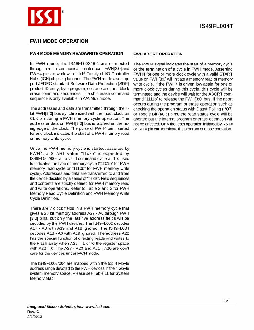
FWH MODE OPERATION (CONTINUED)
Table 2: FWH Memory Read Cycle Definition
Clock Cycle Field FWH[3:0] Direction Description
1
START
1101
IN Start of Cycle: "1101b" to indicate the start of a memory
read cycle.
2
IDSEL
0000 to
1111
IN
ID Select Cycle: Indicates which FWH device should respond.
If the IDSEL field matches the value set on ID[3:0] pins, then
the particular FWH device will respond to subsequent
commands.
3-9
IMADDR
YYYY
IN
Address Cycles: This is the 28-bit memory address. The
addresses transfer most-significant nibble first and least-
significant nibble last. (i.e., A27 - 24 on FWH[3:0] first, and
A3 - A0 on FWH[3:0] last).
10
IMSIZE
0000
IN
Memory Size Cycle: Indicates how many bytes will be or
transferred during multi-byte operations. The IS49FL00x only
support "0000b" for one byte operation.
11
TAR0
1111 IN then
Float Turn-Around Cycle 0: The Intel ICH has driven the bus then
float it to all "1"s and then floats the bus.
12
TAR1 1111
(float) Float then
OUT Turn-Around Cycle 1: The device takes control of the bus
during this cycle.
13
RSYNC 0000
(READY)
OUT Ready Sync: The FWH device indicates the least-significant
nibble of data byte will be ready in next clock cycle.
14-15
DATA
YYYY
OUT
Data Cycles: The 8-bits data transferred with least-significant
nibble first and most-significant nibble last. (i.e., I/O3 - I/O0 on
LAD[3:0] first, then I/O7 - I/O4 on FWH[3:0] last).
16
TAR0
1111 OUT then
Float Turn -Around Cycle 0: The FWH device has driven the bus
then float it to all "1"s and then floats the bus.
17
TAR1 1111
(float) Float then
IN Turn-Around Cycle 1: The Intel ICH resumes control of the bus
during this cycle.
FWH MEMORY READ CYCLE WAVEFORMS
CLK
RST# or INIT#
F W H 4
Memor y
Read
Star t
IDSEL
Address
IMSIZE
TAR
RSY N C
Data
TAR
Next Start
FWH[3:0] 1101b ID[3:0] xxxxb x1xxb
A[19:16] A[15:12] A[11:8] A[7:4] A [3:0]
0000b
1111b Tri-State 0000b D[3:0] D[7:4]
1111b Tri-State
1101b
1 Clock 1 Clock Load Address in 7 Clocks 2 Clocks 1 Clock Data Out 2 Clocks 2 Clocks 1 Clock
From Host to Device
From Device to Host
IS49FL004T
Integrated Silicon Solution, Inc.- www.issi.com
Rev. C
2/1/2013
14
FWH MODE OPERATION (CONTINUED)
Table 3: FWH Memory Write Cycle Definition
Clock Cycle Field FWH[3:0] Direction Description
1
START
1110
IN Start of Cycle: "1110b" to indicate the start of a memory
write cycle.
2
IDSEL
0000 to
1111
IN
ID Select Cycle: Indicates which FWH device should respond.
If the IDSEL field matches the value set on ID[3:0] pins, then
the particular FWH device will respond to subsequent
commands.
3-9
IMADDR
YYYY
IN
Address Cycles: This is the 28-bit memory address. The
addresses transfer most-significant nibble first and least-
significant nibble last. (i.e., A27 - 24 on FWH[3:0] first, and
A3 - A0 on FWH[3:0] last).
10
IMSIZE
0000
IN
Memory Size Cycle: Indicates how many bytes will be or
transferred during multi-byte operations. The IS49FL00x only
support "0000b" for one byte operation.
11-12
DATA
YYYY
IN
Data Cycles: The 8-bits data transferred with least-significant
nibble first and most-significant nibble last. (i.e., I/O3 - I/O0 on
LAD[3:0] first, then I/O7 - I/O4 on FWH[3:0] last).
13
TAR0
1111 IN then
Float Turn-Around Cycle 0: The Intel ICH has driven the bus then
float it to all "1"s and then floats the bus.
14
TAR1 1111
(float) Float then
OUT Turn-Around Cycle 1: The device takes control of the bus
during this cycle.
15
RSYNC 0000
(READY)
OUT Ready Sync: The FWH device indicates that it has received
the data or command.
16
TAR0
1111 OUT then
Float Turn-Around Cycle 0: The FWH device has driven the bus
then float it to all "1"s and then floats the bus.
17
TAR1 1111
(float) Float then
IN Turn-Around Cycle 1: The Intel ICH resumes control of the bus
during this cycle.
FWH MEMORY WRITE CYCLE WAVEFORMS
CLK
RST# or INIT#
F W H 4
Memor y
Wri te
Start IDSEL
FWH[3:0] 1110b ID[3:0] xxxxb
x1xxb
Address
A[19:16] A[15:12] A[11:8] A[7:4] A [3:0]
IMSIZE
0000b
D[3:0]
Data
D[7:4]
T A R RSY NC
1111b Tri-State 0000b
TAR
1111b Tri-State
Next Start
1110b
1 Clock 1 Clock Load Address in 7 Clocks 1 Clock Load Data in 2 Clocks 2 Clocks 1 Clock 2 Clocks 1 Clock
From Host to Device
From Device to Host

IS49FL004T
Integrated Silicon Solution, Inc.- www.issi.com
Rev. C
2/1/2013
15
FWH MODE OPERATION (CONTINUED)
FWH BYTE PROGRAM WAVEFORMS
CLK
RST# or INIT#
F W H 4
Memor y
Wri te
Cycle IDSEL
Address
IMSIZE
Data
T A R RSYN C
TAR
FWH[3:0] 1110b ID[3:0] xxxxb x1xxb xxxxb 0101b 0101b 0101b 0101b 0000b 1010b 1010b 1111b Tri-State 0000b 1111b Tri-State
1 Clock 1 Clock Load "5555h" in 7 Clocks Host to Device
1 Clock Load "AAh" in 2 Clocks 2 Clocks 1 Clock 2 Clocks Device to Host
CLK
RST# or INIT#
F W H 4
2nd Start
IDSEL
Address
IMSIZE
Data
T A R RSY NC
TAR
FWH[3:0] 1110b ID[3:0] xxxxb
x1xxb xxxxb
0010b
1010b
1010b
1010b 0000b
0101b
0101b
1111b Tri-State 0000b
1111b Tri-State
1 Clock 1 Clock Load "2AAAh" in 7 Clocks Host to Device
1 Clock Load "55h" in 2 Clocks 2 Clocks 1 Clock 2 Clocks Device to Host
CLK
RST# or INIT#
F W H 4
3rd Start
IDSEL
Address
IMSIZE
Data
T A R RSY NC
TAR
FWH[3:0] 1110b ID[3:0] xxxxb
x1xxb xxxxb
0101b
0101b
0101b 0101b
0000b
0000b
1010b
1111b Tri-State 0000b
1111b Tri-State
1 Clock 1 Clock Load "5555h" in 7 Clocks Host to Device
1 Clock Load "A0h" in 2 Clocks 2 Clocks 1 Clock 2 Clocks Device to Host
CLK
RST# or INIT#
F W H 4
4th Start
IDSEL
Address
IMSIZE
Data
T A R RSY NC
TAR
FWH[3:0] 1110b ID[3:0] xxxxb
x1xxb
A[19:16] A [15:12]
A[11:8] A[7:4]
A[3:1]
0000b
D[3:0]
D[7:4]
1111b Tri-State 0000b
1111b Tri-State
1 Clock 1 Clock Load Address in 7 Clocks Host to Device
1 Clock Load Data in 2 Clocks 2 Clocks 1 Clock 2 Clocks Device to Host
IS49FL004T
Integrated Silicon Solution, Inc.- www.issi.com
Rev. C
2/1/2013
16
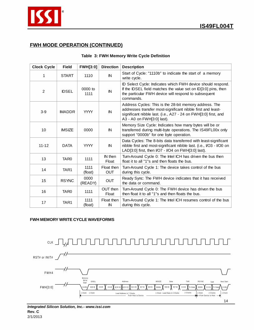
FWH SECTOR ERASE WAVEFORMS
C L K
RST# or INIT#
F W H 4
FWH[3 :0 ]
M em o ry
Wri te Cycl e I DSE L
1110b ID[3:0] xxxxb
x1xxb xxxxb
Address
0 1 0 1b
0 1 0 1b
0 1 0 1b 0 1 0 1b
IM S IZE
0 0 0 0b
D a ta
1 0 1 0b 1 0 1 0b
T A R R S Y N C
1 1 1 1b T r i -S tate 0 0 0 0b
TAR
1 1 1 1b T r i -S tate
1 C loc k 1 C lock Lo a d "55 55 h" in 7 Clocks Hos t to Dev ice
1 C lock Loa d "AAh" in 2 Clocks 2 C locks 1 C lock 2 C locks Dev ice to Hos t
C L K
RST# or INIT#
F W H 4
2nd S tar t I DSE L
Address
IM S IZE
D a ta
T A R R S Y N C
TAR
FWH[3 :0 ] 1110b ID[3:0] xxxxb
x1xxb xxxxb
0 01 0 b
1 01 0 b
1 01 0 b 1 01 0 b 0 0 00 b
0 10 1 b
0 10 1 b
1 11 1 b T r i -S tate 0 0 0 0b
1 11 1 b T r i -S tate
1 C loc k 1 C lock Lo ad "2AAAh " in 7 Clocks Hos t to Device
1 C lock Load "55 h" in 2 Clocks 2 C locks 1 C lock 2 C locks Device to Hos t
C L K
RST# or INIT#
F W H 4
3rd S tar t
I DSE L
Address
IM S IZE
D a ta
T A R R S Y N C
TAR
FWH[3 :0 ] 1110b ID[3:0] xxxxb x1xxb xxxxb
0 10 1 b
0 10 1 b
0 10 1 b 0 10 1 b
0 00 0 b
0 00 0 b 1 00 0 b
1 11 1 b T r i -S tate 0 00 0 b
1 11 1 b T r i -S tate
1 C loc k 1 C lock Lo ad "5 55 5h " in 7 Clocks Hos t to Device
1 C lock Load "80h " in 2 Clocks 2 C locks 1 C lock 2 C locks Device to Hos t
C L K
RST# or INIT#
F W H 4
4th S tar t
I DSE L
Address
IM S IZE
D a ta
T A R R S Y N C
TAR
FWH[3 :0 ] 1110b ID[3:0] xxxxb
x1xxb xxxxb
0 10 1 b
0 10 1 b
0 10 1 b 0 1 01 b 0 00 0 b
0 10 1 b
1 01 0 b
1 11 1 b T r i -S tate 0 0 0 0b
1 11 1 b T r i -S tate
1 Cloc k 1 Clock Loa d "55 5 5" in 7 C locks Hos t to Device
1 C lock Load "AAh" in 2 Clocks 2 C locks 1 C lock 2 C locks Device to Hos t
C L K
RST# or INIT#
F W H 4
5th S tar t
I DSE L
Address
IM S IZE
D a ta
T A R R S Y N C
TAR
FWH[3 :0 ] 1110b ID[3:0] xxxxb
x1xxb xxxxb
0 01 0 b
0 01 0 b
1 01 0 b 1 01 0 b
0 00 0 b
0 10 1 b 0 10 1 b
1 11 1 b T r i -S tate 0 00 0 b
1 11 1 b T r i -S tate
1 C loc k 1 C lock Lo ad "2AAAh " in 7 Clocks Hos t to Device
1 C lock Load "55h " in 2 Clocks 2 C locks 1 C lock 2 C locks Device to Hos t
C L K
RST# or INIT#
F W H 4
6th S tar t
I DSE L
Address
IM S IZE
D a ta
T A R R S Y N C
TAR
In terna l Erase
S tar t
FWH[3:0 ] 1110b ID[3:0] xxxxb
x1xxb xxxxb
S A [19 :16 ] S A [15:12 ]
xxxxb xxxxb
0 00 0 b
0 00 0 b
0 01 1 b
1 11 1 b T r i -S tate 0 0 0 0b
1 11 1 b T r i -S tate
1 Cloc k 1 Clock L oa d Sec t or Addr ess in 7 Clocks Hos t to Device
SA = S ec tor A ddr ess 1 C lock
Load
"30h" in 2 Clocks

IS49FL004T
Integrated Silicon Solution, Inc.- www.issi.com
Rev. C
2/1/2013
17
2 C locks 1 C lock 2
Clo
cks
Dev ice to Hos t

IS49FL004T
Integrated Silicon Solution, Inc.- www.issi.com
Rev. C
2/1/2013
18
FWH BLOCK ERASE WAVEFORMS
C L K
RST# or INIT#
F W H 4
FWH[3 :0 ]
M em o ry
Wri te Cycl e I DSE L
1110b ID[3:0] xxxxb
x1xxb xxxxb
Address
0 1 0 1b
0 1 0 1b
0 1 0 1b 0 1 0 1b
IM S IZE
0 0 0 0b
D a ta
1 0 1 0b 1 0 1 0 b
T A R R S Y N C
1 1 1 1b T r i -S tate 0 0 0 0b
TAR
1 1 1 1b T r i -S tate
1 C loc k 1 C lock L oa d "55 55 h " in 7 Clocks Hos t to Dev ice
1 C lock Loa d "AAh" in 2 Clocks 2 C locks 1 C lock 2 C locks Dev ice to Hos t
C L K
RST# or INIT#
F W H 4
2nd S tar t I D SE L
Address
IM S IZE
D a ta
T A R R S Y N C
TAR
FWH[3 :0 ] 1110b ID[3:0] xxxxb
x1xxb xxxxb
0 01 0 b
1 01 0 b
1 01 0 b 1 01 0 b 0 0 00 b
0 10 1 b
0 10 1 b
1 11 1 b T r i -S tate 0 00 0 b
1 11 1 b T r i -S tate
1 C loc k 1 C lock Lo ad "2AAAh " in 7 Clocks Hos t to Device
1 C lock Load "55 h" in 2 Clocks 2 C locks 1 C lock 2 C locks Device to Hos t
C L K
RST# or INIT#
F W H 4
3rd S tar t
I DSE L
Address
IM S IZE
D a ta
T A R R S Y N C
TAR
FWH[3 :0 ] 1110b ID[3:0] xxxxb x1xxb xxxxb
0 10 1 b
0 10 1 b
0 10 1 b 0 10 1 b
0 00 0 b
0 00 0 b 1 0 00 b
1 11 1 b T r i -S tate 0 00 0 b
1 11 1 b T r i -S tate
1 C loc k 1 C lock Lo ad "5 55 5h " in 7 Clocks Hos t to Device
1 C lock Load "80h " in 2 Clocks 2 C locks 1 C lock 2 C locks Device to Hos t
C L K
RST# or INIT#
F W H 4
4th S tar t
I DSE L
Address
IM S IZE
D a ta
T A R R S Y N C
TAR
FWH[3 :0 ] 1110b ID[3:0] xxxxb
x1xxb xxxxb
0 10 1 b
0 10 1 b
0 10 1 b 0 1 0 1b 0 00 0 b
0 10 1 b
1 01 0 b
1 11 1 b T r i -S tate 0 00 0 b
1 11 1 b T r i -S tate
1 Cloc k 1 Clock Loa d "55 5 5" in 7 C locks Hos t to Device
1 C lock Load "AAh" in 2 Clocks 2 C locks 1 C lock 2 C locks Device to Hos t
C L K
RST# or INIT#
F W H 4
5th S tar t
I DSE L
Address
IM S IZE
D a ta
T A R R S Y N C
TAR
FWH[3 :0 ] 1110b ID[3:0] xxxxb
x1xxb xxxxb
0 01 0 b
0 01 0 b
1 01 0 b 1 01 0 b
0 00 0 b
0 10 1 b 0 1 01 b
1 11 1 b T r i -S tate 0 00 0 b
1 11 1 b T r i -S tate
1 C loc k 1 C lock Lo ad "2AAAh " in 7 Clocks Hos t to Device
1 C lock Load "55h " in 2 Clocks 2 C locks 1 C lock 2 C locks Device to Hos t
C L K
RST# or INIT#
F W H 4
6th S tar t
I DSE L
Address
IM S IZE
D a ta
T A R R S Y N C
TAR
In terna l Erase
S tar t
FWH[3:0 ] 1110b ID[3:0] xxxxb
x1xxb xxxxb B A [19 :16 ]
B A [15:14 ] + xxb
xxxxb xxxxb
0 00 0 b
0 00 0 b
0 10 1 b
1 1 1 1b T r i -S tate 0 0 0 0b
1 1 1 1b T r i -S tate
1 Cloc k 1 Clock Lo a d B lock Address in 7 Clocks Hos t to Device
BA

IS49FL004T
Integrated Silicon Solution, Inc.- www.issi.com
Rev. C
2/1/2013
19
= B lock A ddr es s 1 C lock Load "50h " in 2 Clocks 2 C locks 1 C lock 2 C locks
Dev ice to Hos t

IS49FL004T
Integrated Silicon Solution, Inc.- www.issi.com
Rev. C
2/1/2013
20
FWH MODE OPERATION (CONTINUED)
FWH GPI REGISTER READ WAVEFORMS
CLK
RST# or INIT#
F W H 4
Memor y
Read
Cycle
IDSEL
Address
IMSIZE
TAR
RSY N C
Data
TAR
Next Start
FWH[3:0] 1101b ID[3:0] xxxxb
x0xxb 1100b 0000b 0001b 0000b 0000b 0000b 1111b Tri-State 0000b D[3:0 ] D[7:4] 1111b Tri-State
1101b
1 Clock 1 Clock Load Address "xBC0100h" in 7 Clocks 1 Clock 2 Clocks 1 Clock Data Out 2 Clocks 2 Clocks 1 Clock
From Host to Device
From Device to Host
FWH BLOCK LOCKING REGISTER READ WAVEFORMS
CLK
RST# or INIT#
F W H 4
Memor y
Read
Cycle
IDSEL
Address
IMSIZE
TAR
RSY N C
Data
TAR
Next Start
FWH[3:0] 1101b ID[3:0] xxxxb
x0xxb A [19:16] 0000b 0000b 0000b 0010b 0000b 1111b Tri-State 0000b D[3:0] D[7:4] 1111b Tri-State
1101b
1 Clock 1 Clock Load Address "xBx0002h" in 7 Clocks 1 Clock 2 Clocks 1 Clock Data Out 2 Clocks 2 Clocks 1 Clock
From Host to Device
From Device to Host

IS49FL004T
Integrated Silicon Solution, Inc.- www.issi.com
Rev. C
2/1/2013
21
LPC MODE OPERATION
LPC MODE MEMORY READ/WRITE OPERATION
In LPC mode, the IS49FL002/004 use the 5-pin LPC
interface includes 4-bit LAD[3:0] and LFRAME# pins to
communicate with the host system. The addresses and
data are transmitted through the 4-bit LAD[3:0] bus syn-
chronized with the input clock on CLK pin during a LPC
memory cycle operation. The address or data on LAD[3:
0] bus is latched on the rising edge of the clock. The
pulse of LFRAME# signal inserted for one or more clocks
indicates the start of a LPC memory read or write cycle.
Once the LPC memory cycle is started, asserted by
LFRAME#, a START value “0000b” is expected by the
devices as a valid command cycle. Then a CYCTYPE +
DIR value (“010xb” for memory read cycle or “011xb” for
memory write cycle) is used to indicates the type of
memory cycle. Refer to Table 4 and 5 for LPC Memory
Read and Write Cycle Definition.
There are 8 clock fields in a LPC memory cycle that
gives a 32 bit memory address A31 - A0 through LAD[3:
0] with the most-significant nibble first. The memory
space of IS49FL002/004 are mapped directly to top of
4 Gbyte system memory space. See Table 11 for Sys-
tem Memory Map.
The IS49FL002 is mapped to the address location of
(FFFFFFFFh - FFFC0000h), the A31- A18 must be
loaded with “1” to select and activate the device during a
LPC memory read or write operation. Only A17 - A0 is
used to decode and access the 256 Kbyte memory. The
I/O7 - I/O0 data is loaded onto LAD[3:0] in 2 clock cycles
with least-significant nibble first and most-significant
nibble last.
The IS49FL004 is mapped to the address location of
(FFFFFFFFh - FFF80000h), the A31- A19 must be
loaded with “1” to select and activate the device during a
LPC memory operation. Only A18 - A0 is used to de-
code and access the 512 Kbyte memory.

IS49FL004T
Integrated Silicon Solution, Inc.- www.issi.com
Rev. C
2/1/2013
22
LPC MODE OPERATION (CONTINUED)
Table 4: LPC Memory Read Cycle Definition
Clock Cycle Field LAD[3:0] Direction Description
1
START
0000
IN Start of Cycle: "0000b" indicates the start of a LPC memory
cycle.
2
CYCTYPE
+
DIR
010x
IN
Cycle Type: Indicates the type of a LPC memory read cycle.
CYCTYPE: Bits 3 - 2 must be "01b" for memory cycle. DIR:
Bit 1 = "0b" indicates the type of cycle for Read. Bit 0 is
reserved.
3 - 10
ADDR
YYYY
IN
Address Cycles: This is the 32-bit memory address. The
addresses transfer most-significant nibble first and least-
significant nibble last. (i.e., A31 - 28 on LAD[3:0] first, and A3
- A0 on LAD[3:0] last).
11
TAR0
1111 IN then
Float Turn-Around Cycle 0: The Chipset has driven the bus to all
"1"s and then float the bus.
12
TAR1 1111
(float) Float then
OUT Turn-Around Cycle 1: The device takes control of the bus
during this cycle.
13
SYNC
0000
OUT Sync: The device indicates the least-significant nibble of data
byte will be ready in next clock cycle.
14 - 15
DATA
YYYY
OUT
Data Cycles: The 8-bits data transferred with least-significant
nibble first and most-significant nibble last. (i.e., I/O3 - I/O0 on
LAD[3:0] first, then I/O7 - I/O4 on LAD[3:0] last).
16
TAR0
1111 OUT then
Float Turn-Around Cycle 0: The device has driven the bus to all
"1"s and then floats the bus.
17
TAR1 1111
(float) Float then
IN Turn-Around Cycle 1: The Chipset resumes control of the bus
during this cycle.
LPC MEMORY READ CYCLE WAVEFORMS
CLK
RST# or INIT#
LFRAME#
Star t
Memor y
Read
Cycle
Address
TAR
SYNC
Data
TAR
Next Start
LAD[3:0] 0000b 010Xb 1111b
1111b 1111b
11b + A[17:16]
A[15:12] A[11:8] A[7:4] A[3:0] 1111b Tri-State 0000b D[3:0] D[7:4]
1111b Tri-State
0000b
1 Clock 1 Clock Load Address in 8 Clocks 2 Clocks 1 Clock Data Out 2 Clocks 2 Clocks 1 Clock
From Host to Device
From Device to Host

IS49FL004T
Integrated Silicon Solution, Inc.- www.issi.com
Rev. C
2/1/2013
23
LPC MODE OPERATION (CONTINUED)
Table 5: LPC Memory Write Cycle Definition
Clock Cycle Field LAD[3:0] Direction Description
1
START
0000
IN Start of Cycle: "0000b" to indicate the start of a LPC
memory cycle.
2
CYCTYPE
+
DIR
011x
IN
Cycle Type: Indicates the type of a LPC memory write cycle.
CYCTYPE: Bits 3 - 2 must be "01b" for memory cycle. DIR:
Bit 1 = "1b" indicates the type of cycle for Write. Bit 0 is
reserved.
3 - 10
ADDR
YYYY
IN
Address Cycles: This is the 32-bit memory address. The
addresses transfer most-significant nibble first and least-
significant nibble last. (i.e., A31 - 28 on LAD[3:0] first, and A3
- A0 on LAD[3:0] last).
11 - 12
DATA
YYYY
IN
Data Cycles: The 8-bits data transferred with least-significant
nibble first and most-significant nibble last. (i.e., I/O3 - I/O0 on
LAD[3:0] first, then I/O7 - I/O4 on LAD[3:0] last).
13
TAR0
1111 IN then
Float Turn-Around Cycle 0: The Chipset has driven the bus to all
"1"s and then float the bus.
14
TAR1 1111
(float) Float then
OUT Turn-Around Cycle 1: The device takes control of the bus
during this cycle.
15
SYNC
0000
OUT Sync: The device indicates that it has received the data or
command.
16
TAR0
1111 OUT then
Float Turn-Around Cycle 0: The device has driven the bus to all
"1"s and then floats the bus.
17
TAR1 1111
(float) Float then
IN Turn-Around Cycle 1: The Chipset resumes control of the bus
during this cycle.
LPC MEMORY WRITE CYCLE WAVEFORMS
CLK
RST# or INIT#
LFRAME#
Star t
Memor y
Wri te
Cycle
Address
Data
TAR SYNC
TAR
Next Start
LAD[3:0] 0000b 011Xb 1111b
1111b 1111b
A[19:16] A[15:12] A[11:8] A[7:4] A[3:0] D[3:0]
D[7:4]
1111b Tri-State 0000b
1111b Tri-State
0000b
1 Clock 1 Clock Load Address in 8 Clocks Load Data in 2 Clocks 2 Clocks 1 Clock 2 Clocks 1 Clock
From Host to Device
From Device to Host

IS49FL004T
Integrated Silicon Solution, Inc.- www.issi.com
Rev. C
2/1/2013
24
LPC MODE OPERATION (CONTINUED)
LPC BYTE PROGRAM WAVEFORMS
CLK
RST# or INIT#
LFRAME #
1st S tart
Memor y
Wri te
Cycle
Address
Data
TAR Sync
TAR
LAD[3:0] 0000b 011Xb 1111b 1111b 1111b 11xxb 0101b 0101b 0101b 0101b 1010b 1010b 1111b Tri-State 0000b 1111b Tri-State
1 Clock 1 Clock Load "5555h" in 8 Clocks Load "AAh" in 2 Clocks Host to Device
2 Clocks 1 Clock 2 Clocks Device to Host
CLK
RST# or INIT#
LFRAME #
2nd Start
Memor y
Wri te Cycle
Address
Data
TAR Sync
TAR
LAD[3:0] 0000b 011Xb 1111b 1111b 1111b 11xxb 0010b 1010b 1010b 1010b 0101b 0101b 1111b Tri-State 0000b 1111b Tri-State
1 Clock 1 Clock Load "2AAAh" in 8 Clocks Load "55h" in 2 Clocks Host to Device
2 Clocks 1 Clock 2 Clocks Device to Host
CLK
RST# or INIT#
LFRAME #
3rd Start
Memor y
Wri te
Cycle
Address
Data
TAR Sync
TAR
LAD[3:0] 0000b 011Xb 1111b 1111b 1111b 11xxb 0101b 0101b 0101b 0101b 0000b 1010b 1111b Tri-State 0000b 1111b Tri-State
1 Clock 1 Clock Load "5555h" in 8 Clocks Load "A0h" in 2 Clocks Host to Device
2 Clocks 1 Clock 2 Clocks Device to Host
CLK
RST# or INIT#
LFRAME #
4th Start
Memor y
Wri te
Cycle
Address
Data
TAR Sync
TAR
LAD[3:0] 0000b 011Xb 1111b 1111b 1111b A[19:16] A [15:12] A[11:8] A[7:4] A[3:1] D[3:0] D[7:4] 1111b Tri-State 0000b 1111b Tri-State
1 Clock 1 Clock Load Address in 8 Clocks Load Data in 2 Clocks Host to Device
2 Clocks 1 Clock 2 Clocks Device to Host

IS49FL004T
Integrated Silicon Solution, Inc.- www.issi.com
Rev. C
2/1/2013
25
LPC SECTOR ERASE WAVEFORMS
C L K
RST# or INIT#
L F R AM E #
1s t S tar t
M em o ry
Wr i te
Cycle
Address
D a ta
T A R Sy nc
TAR
LAD[3:0 ] 0 0 0 0b 0 1 1X b 1 1 1 1 b
1 1 1 1b 1 1 1 1 b
11xxb
0 1 0 1b
0 1 0 1b 0 1 0 1b 0 1 0 1b 1 0 1 0b 1 0 1 0 b 1 1 1 1b T r i -S tate 0 0 0 0b 1 1 1 1b T r i -S tate
1 C loc k 1 C lock L oa d "55 55 h " in 8 Clocks Load "AAh" in 2 Clocks Hos t to Dev ice
2 C locks 1 C lock 2 C locks Dev ice to Hos t
C L K
RST# or INIT#
L F R AM E #
2nd S tar t
M em o ry
Wr i te
Cyc le
Address
D a ta
T A R Sy nc
TAR
LAD[3:0 ] 0 00 0 b 0 1 1X b 1 1 1 1b 1 11 1 b 1 1 1 1b 11xxb 0 01 0 b
1 01 0 b 1 01 0 b 1 0 10 b 0 10 1 b 0 10 1 b
1 11 1 b T r i -S tate 0 00 0 b
1 11 1 b T r i -S tate
1 C loc k 1 C lock Lo ad "2AAAh " in 8 Clocks Load "55 h" in 2 Clocks Hos t to Device
2 C locks 1 C lock 2 C locks Device to Hos t
C L K
RST# or INIT#
L F R AM E #
3rd S tar t
M em ory
Wr i te
Cyc le
Address
D a ta
T A R Sy nc
TAR
LAD[3:0 ] 0 00 0 b 0 1 1X b 1 1 1 1b 1 11 1 b 1 1 1 1b 11xxb 0 10 1 b
0 10 1 b 0 10 1 b 0 10 1 b 0 00 0 b 1 0 00 b 1 11 1 b T r i -S tate 0 00 0 b 1 11 1 b T r i -S tate
1 C loc k 1 C lock Lo ad "5 55 5h " in 8 Clocks Loa d "80h " in 2 Clocks Hos t to Device
2 C locks 1 C lock 2 C locks Device to Hos t
C L K
RST# or INIT#
L F R AM E #
4th S tar t
M em ory
Wr i te
Cyc le
Address
D a ta
T A R Sy nc
TAR
LAD[3:0 ] 0 00 0 b 0 1 1X b 1 1 1 1b 1 11 1 b 1 1 1 1b 11xxb 0 10 1 b 0 10 1 b 0 1 0 1b 0 10 1 b 0 10 1 b 1 01 0 b 1 11 1 b T r i -S tate 0 00 0 b
1 11 1 b T r i -S tate
1 Cloc k 1 Clock Loa d "55 5 5" in 8 C locks Load "AAh" in 2 Clocks Hos t to Device
2 C locks 1 C lock 2 C locks Device to Hos t
C L K
RST# or INIT#
L F R AM E #
5th S tar t
M em ory
Wr i te
Cyc le
Address
D a ta
T A R Sy nc
TAR
LAD[3:0 ] 0 00 0 b 0 1 1X b 1 1 1 1b 1 11 1 b 1 1 1 1b 11xxb 0 01 0 b
1 01 0 b 1 01 0 b 1 01 0 b 0 10 1 b 0 1 01 b 1 11 1 b T r i -S tate 0 00 0 b 1 11 1 b T r i -S tate
1 C loc k 1 C lock Lo ad "2AAAh " in 8 Clocks Load "55 h" in 2 Clocks Hos t to Device
2 C locks 1 C lock 2 C locks Device to Hos t
C L K
RST# or INIT#
L F R AM E #
6th S tar t
M em ory
Wr i te
Cyc le
Address
D a ta
T A R Sy nc
TAR
In terna l Erase
S tar t
LAD[3:0 ] 000 0 b 0 1 1X b 1 1 11 b 1 11 1 b 1 1 1 1b S A [19 :16 ] S A [15 :12 ] xxxxb xxxxb xxxxb 0 0 0 0b 0 0 1 1b 1 1 1 1b T r i -S tate 0 0 0 0b
1 1 1 1b T r i -S tate
1 Cloc k 1 Clock Lo ad S ec tor Ad dress in 8 Clocks Load "30h " in 2 Clocks 2 C locks 1 C lock 2 C locks

IS49FL004T
Integrated Silicon Solution, Inc.- www.issi.com
Rev. C
2/1/2013
26
Hos t to Device
Device to Hos t
SA = S ec tor A ddr es s

IS49FL004T
Integrated Silicon Solution, Inc.- www.issi.com
Rev. C
2/1/2013
27
LPC BLOCK ERASE WAVEFORMS
C L K
RST# or INIT#
L F R AM E #
1s t S tar t
M em o ry
Wr i te
Cycle
Address
D a ta
T A R Sy nc
TAR
LAD[3:0 ] 0 0 0 0b 0 1 1X b 1 1 1 1 b 1 1 1 1b 1 1 1 1 b
11xxb
0 1 0 1b
0 1 0 1b 0 1 0 1b 0 1 0 1b 1 0 1 0b 1 0 1 0 b 1 1 1 1b T r i -S tate 0 0 0 0b 1 1 1 1b T r i -S tate
1 C loc k 1 C lock L oa d "55 55 h " in 8 Clocks Load "AAh" in 2 Clocks Hos t to Dev ice
2 C locks 1 C lock 2 C locks Dev ice to Hos t
C L K
RST# or INIT#
L F R AM E #
2nd S tar t
M em o ry
Wr i te
Cyc le
Address
D a ta
T A R Sy nc
TAR
LAD[3:0 ] 0 00 0 b 0 1 1X b 1 1 1 1b 1 11 1 b 1 1 1 1b 11xxb 0 01 0 b
1 01 0 b 1 01 0 b 1 0 10 b 0 10 1 b 0 10 1 b
1 11 1 b T r i -S tate 0 00 0 b 1 11 1 b T r i -S tate
1 C loc k 1 C lock Lo ad "2AAAh " in 8 Clocks Load "55 h" in 2 Clocks Hos t to Device
2 C locks 1 C lock 2 C locks Device to Hos t
C L K
RST# or INIT#
L F R AM E #
3rd S tar t
M em ory
Wr i te
Cyc le
Address
D a ta
T A R Sy nc
TAR
LAD[3:0 ] 0 00 0 b 0 1 1X b 1 1 1 1b 1 11 1 b 1 1 1 1b 11xxb 0 10 1 b
0 10 1 b 0 10 1 b 0 10 1 b 0 00 0 b 1 0 00 b 1 11 1 b T r i -S tate 0 00 0 b 1 11 1 b T r i -S tate
1 C loc k 1 C lock Lo ad "5 55 5h " in 8 Clocks Loa d "80h " in 2 Clocks Hos t to Device
2 C locks 1 C lock 2 C locks Device to Hos t
C L K
RST# or INIT#
L F R AM E #
4th S tar t
M em ory
Wr i te
Cyc le
Address
D a ta
T A R Sy nc
TAR
LAD[3:0 ] 0 00 0 b 0 1 1X b 1 1 1 1b 1 11 1 b 1 1 1 1b 11xxb 0 10 1 b 0 10 1 b 0 1 0 1b 0 10 1 b 0 10 1 b 1 01 0 b 1 11 1 b T r i -S tate 0 00 0 b 1 11 1 b T r i -S tate
1 Cloc k 1 Clock Loa d "55 5 5" in 8 C locks Load "AAh" in 2 Clocks Hos t to Device
2 C locks 1 C lock 2 C locks Device to Hos t
C L K
RST# or INIT#
L F R AM E #
5th S tar t
M em ory
Wr i te
Cyc le
Address
D a ta
T A R Sy nc
TAR
LAD[3:0 ] 0 00 0 b 0 1 1X b 1 1 1 1b 1 11 1 b 1 1 1 1b 11xxb 0 01 0 b
1 01 0 b 1 01 0 b 1 01 0 b 0 10 1 b 0 1 01 b 1 11 1 b T r i -S tate 0 00 0 b 1 11 1 b T r i -S tate
1 C loc k 1 C lock Lo ad "2AAAh " in 8 Clocks Load "55 h" in 2 Clocks Hos t to Device
2 C locks 1 C lock 2 C locks Device to Hos t
C L K
RST# or INIT#
L F R AM E #
6th S tar t
M em ory
Wr i te
Cyc le
Address
D a ta
T A R Sy nc
TAR
In terna l Erase
S tar t
LAD[3:0 ] 000 0b 0 1 1X b 1 1 1 1 b 1 1 1 1b 1 1 11 b B A [19 :16 ] B A [15:14 ] + xxb
xxxxb xxxxb xxxxb 0 0 0 0b 0 10 1 b 1 11 1 b T r i -S tate 0 00 0 b 1 11 1 b T r i -S tate
1 Cloc k 1 Clock Lo a d B lock Address in 8 Clocks Load "50h " in 2 Clocks Ho
st

IS49FL004T
Integrated Silicon Solution, Inc.- www.issi.com
Rev. C
2/1/2013
28
to Dev ice
BA = B lock Ad dres s 2 C locks 1 C lock 2 C locks
Dev ice to Hos t

IS49FL004T
Integrated Silicon Solution, Inc.- www.issi.com
Rev. C
2/1/2013
29
LPC MODE OPERATION (CONTINUED)
LPC GPI REGISTER READ WAVEFORMS
CLK
RST# or INIT#
LFRAME#
Star t
Memor y
Read
Cycle
Address
TAR
SYNC
Data
TAR
Next Start
LAD[3:0] 0000b 010Xb 1111b
1111b 1011b
1100b 0000b 0001b 0000b 0000b 1111b Tri-State 0000b D[3:0] D[7:4]
1111b Tri-State
0000b
1 Clock 1 Clock Load Address "FFBC0100h" in 8 Clocks 2 Clocks 1 Clock Data Out 2 Clocks 2 Clocks 1 Clock
From Host to Device
From Device to Host
IS49FL004T
Integrated Silicon Solution, Inc.- www.issi.com
Rev. C
2/1/2013
30
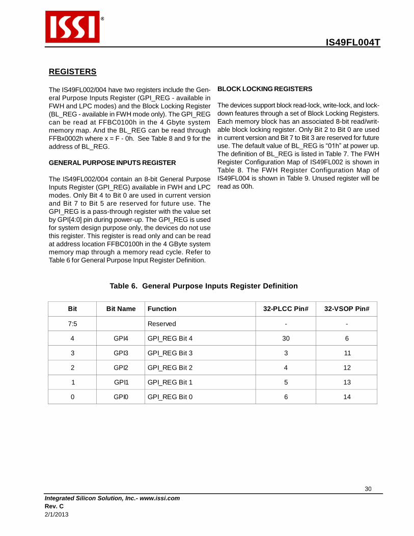
REGISTERS
The IS49FL002/004 have two registers include the Gen-
eral Purpose Inputs Register (GPI_REG - available in
FWH and LPC modes) and the Block Locking Register
(BL_REG - available in FWH mode only). The GPI_REG
can be read at FFBC0100h in the 4 Gbyte system
memory map. And the BL_REG can be read through
FFBx0002h where x = F - 0h. See Table 8 and 9 for the
address of BL_REG.
GENERAL PURPOSE INPUTS REGISTER
The IS49FL002/004 contain an 8-bit General Purpose
Inputs Register (GPI_REG) available in FWH and LPC
modes. Only Bit 4 to Bit 0 are used in current version
and Bit 7 to Bit 5 are reserved for future use. The
GPI_REG is a pass-through register with the value set
by GPI[4:0] pin during power-up. The GPI_REG is used
for system design purpose only, the devices do not use
this register. This register is read only and can be read
at address location FFBC0100h in the 4 GByte system
memory map through a memory read cycle. Refer to
Table 6 for General Purpose Input Register Definition.
BLOCK LOCKING REGISTERS
The devices support block read-lock, write-lock, and lock-
down features through a set of Block Locking Registers.
Each memory block has an associated 8-bit read/writ-
able block locking register. Only Bit 2 to Bit 0 are used
in current version and Bit 7 to Bit 3 are reserved for future
use. The default value of BL_REG is “01h” at power up.
The definition of BL_REG is listed in Table 7. The FWH
Register Configuration Map of IS49FL002 is shown in
Table 8. The FWH Register Configuration Map of
IS49FL004 is shown in Table 9. Unused register will be
read as 00h.
Table 6. General Purpose Inputs Register Definition
Bit Bit Name Function 32-PLCC Pin# 32-VSOP Pin#
7:5
Reserved
-
-
4
GPI4
GPI_REG Bit 4
30
6
3
GPI3
GPI_REG Bit 3
3
11
2
GPI2
GPI_REG Bit 2
4
12
1 GPI1 GPI_REG Bit 1 5 13
0 GPI0 GPI_REG Bit 0 6 14

IS49FL004T
Integrated Silicon Solution, Inc.- www.issi.com
Rev. C
2/1/2013
31
REGISTERS (CONTINUED)
Table 7. Block Locking Register Definition
Bit Function
7:3 Reserved
2
Read-Lock
"1" = Prevents read operations in the block where set.
"0" = Normal operation for reads in the block where clear. Default state.
1
Lock-Down
"1" = Prevents further set or clear operations to the Write-Lock and Read-Lock bits. Lock-
Down only can be set, but not cleared. The block will remain locked-down until reset (with
RST# or INIT#), or until the device is power-on reset.
"0" = Normal operation for Write-Lock and Read-Lock bit altering in the block where clear.
Default state.
0
Write-Lock
"1" = Prevents program or erase operations in the block where set. Default state.
"0" = Normal operation for programming and erase in the block where clear.
Data Bit[7:3] Bit 2 Bit 1 Bit 0 Resulting Block State
00h
00000
0
0
0
Full access.
01h
00000
0
0
1
Write locked. Default state at power-up.
02h
00000
0
1
0
Locked open (full access locked down).
03h
00000
0
1
1
Write-locked down.
04h
00000
1
0
0
Read locked.
05h
00000
1
0
1
Read and write locked.
06h
00000
1
1
0
Read-locked down.
07h
00000
1
1
1
Read-locked and write-locked down.

IS49FL004T
Integrated Silicon Solution, Inc.- www.issi.com
Rev. C
2/1/2013
32
REGISTERS (CONTINUED)
Table 8. IS49FL002 Block Locking Register Address
Register
Block Size
(Kbytes) Protected Block
Address Range
Memory Map Address
T_BLOCK_LK 16 3C000h - 3FFFFh FFBF8002h
T_MINUS01_LK
16
16
16
38000h - 3BFFFh
34000h - 37FFFh
30000h - 33FFFh
FFBF0002h
T_MINUS02_LK
16
16 2C000h - 2FFFFh
28000h - 2BFFFh
FFBE8002h
T_MINUS03_LK
16
16 24000h - 27FFFh
20000h - 23FFFh
FFBE0002h
T_MINUS04_LK
16
16 1C000h - 1FFFFh
18000h - 1BFFFh
FFBD8002h
T_MINUS05_LK
16
16 14000h - 17FFFh
10000h - 13FFFh
FFBD0002h
T_MINUS06_LK
16
16 0C000h - 0FFFFh
08000h - 0BFFFh
FFBC8002h
T_MINUS07_LK
16
16 04000h - 07FFFh
00000h - 03FFFh
FFBC0002h
Table 9. IS49FL004 Block Locking Register Address
Register Block Size
(Kbytes) Protected Block
Address Range
Memory Map Address
T_BLOCK_LK 64 70000h - 7FFFFh FFBF0002h
T_MINUS01_LK 64 60000h - 6FFFFh FFBE0002h
T_MINUS02_LK 64 50000h - 5FFFFh FFBD0002h
T_MINUS03_LK 64 40000h - 4FFFFh FFBC0002h
T_MINUS04_LK 64 30000h - 3FFFFh FFBB0002h
T_MINUS05_LK 64 20000h - 2FFFFh FFBA0002h
T_MINUS06_LK 64 10000h - 1FFFFh FFB90002h
T_MINUS07_LK 64 00000h - 0FFFFh FFB80002h

IS49FL004T
Integrated Silicon Solution, Inc.- www.issi.com
Rev. C
2/1/2013
33
A/A MUX MODE OPERATION
A/A MUX MODE READ/WRITE OPERATION
The IS49FL002/004 offers a Address/Address Multi-
plexed (A/A Mux) mode for off-system operation, typi-
cally on an EPROM Programmer, similar to a traditional
Flash memory except the address input is multiplexed.
In the A/A Mux mode, the programmer must drive the
OE# pin to low (VIL) for read or WE# pins to low for write
operation. The devices have no Chip Enable (CE#) pin
for chip selection and activation as traditional Flash
memory. The R/C#, OE# and WE# pins are used to
activate the device and control the power. The 11 multi-
plex address pins - A[10:0] and a R/C# pin are used to
load the row and column addresses for the target memory
location. The row addresses (internal address A10 - A0)
are latched on the falling edge of R/C# pin. The column
addresses (internal address A21 - A11) are latched on
the rising edge of R/C# pin. The IS49FL002 uses A17
- A0 internally to decode and access the 256 Kbytes
memory space. The IS49FL004 use A18 - A0
respectively.
During a read operation, the OE# signal is used to con-
trol the output of data to the 8 I/O pins - I/O[7:0]. During
a write operation, the WE# signal is used to latch the
input data from I/O[7:0]. See Table 10 for Bus Operation
Modes.
Table 10. A/A Mux Mode Bus Operation Modes
Mode RST# OE# WE# Address I/O
Read VIH VIL VIH X (1) DOUT
Write VIH VIH VIL
X DIN
Standby VIH VIH VIH
X
High Z
Output Disable VIH VIH
X
X
High Z
Reset VIL
X
X
X
High Z
Product Identification
VIH
VIL
VIH
A2 - A21 = X,
A1 = VIL, A0 = VIL
and A1 = VIH, A0 = VIH
Manufacturer ID (2)
A2 - A21 = X,
A1 = VIL, A0 = VIH
Device ID (2)
Notes:
1. X can be VIL or VIH.
2. Refer to Table 1 for the Manufacturer ID and Device ID of devices.

IS49FL004T
Integrated Silicon Solution, Inc.- www.issi.com
Rev. C
2/1/2013
34
SYSTEM MEMORY MAP
Sys tem M em ory
(Top 4 MBy tes)
FF FF FF FF h
F F F C 0 0 0 0 h
FF F8 0 0 0 0 h
FF F0 0 0 0 0 h
IS 4 9 F L 0 0 2
(2 Mbi ts)
IS 4 9 F L 0 0 4
(4 Mbi ts)
IS 4 9 F L 0 0 8
(8 Mbi ts)
Range for other
FW H D ev i ce s
FF C 0 00 0 0 h
Table 11. System Memory Map

IS49FL004T
Integrated Silicon Solution, Inc.- www.issi.com
Rev. C
2/1/2013
35
MEMORY BLOCKS AND ADDRESSES
Table 12. IS49FL002 Sector/Block Address Table
Hardware
Protection
Block
Block Size
(Kbytes)
Sector
Sector Size
(Kbytes)
Address Range
TBL#
Block 15 (Boot
Block)
16
"
"
3C000h - 3FFFFh
WP#
Block 14
16 " "
38000h - 3BFFFh
Block 13
16 " "
34000h - 37FFFh
Block 12
16 " "
30000h - 33FFFh
Block 11
16 " "
2C000h - 2FFFFh
Block 10
16 " "
28000h - 2BFFFh
Block 9
16 " "
24000h - 27FFFh
Block 8
16 " "
20000h - 23FFFh
Block 7
16 " "
1C000h - 1FFFFh
Block 6
16 " "
18000h - 1BFFFh
Block 5
16 " "
14000h - 17FFFh
Block 4
16 " "
10000h - 13FFFh
Block 3
16 " "
0C000h - 0FFFFh
Block 2
16 " "
08000h - 0BFFFh
Block 1
16 " "
04000h - 07FFFh
Block 0
16
Sector 3
4
03000h - 03FFFh
Sector 2
4
02000h - 02FFFh
Sector 1
4
01000h - 01FFFh
Sector 0
4
00000h - 00FFFh

IS49FL004T
Integrated Silicon Solution, Inc.- www.issi.com
Rev. C
2/1/2013
36
MEMORY BLOCKS AND ADDRESSES (CONTINUED)
Table 13. IS49FL004 Sector/Block Address Table
Hardware
Protection
Block
Block Size
(Kbytes)
Sector
Sector Size
(Kbytes)
Address Range
TBL#
Block 7 (Boot
Block)
64
"
"
70000h - 7FFFFh
WP#
Block 6
64 " "
60000h - 6FFFFh
Block 5
64 " "
50000h - 5FFFFh
Block 4
64 " "
40000h - 4FFFFh
Block 3
64 " "
30000h - 3FFFFh
Block 2
64 " "
20000h - 2FFFFh
Block 1
64 " "
10000h - 1FFFFh
Block 0
64
Sector 15
4
0F000h - 0FFFFh
: : :
Sector 1
4
01000h - 01FFFh
Sector 0
4
00000h - 00FFFh

IS49FL004T
Integrated Silicon Solution, Inc.- www.issi.com
Rev. C
2/1/2013
37
MS MS
COMMAND DEFINITION
Table 14. Software Data Protection Command Definition
Command
Sequence
Bus
Cycle
1st Bus
Cycle
Addr(2) Data
2nd Bus
Cycle
Addr Data
3rd Bus
Cycle
Addr Data
4th Bus
Cycle
Addr Data
5th Bus
Cylce
Addr Data
6th Bus
Cycle
Addr Data
Read 1 Addr DOUT
Chip Erase (1) 6 5555h AAh 2AAAh 55h 5555h 80h 5555h AAh 2AAAh 55h 5555h 10h
Sector Erase 6 5555h AAh 2AAAh 55h 5555h 80h 5555h AAh 2AAAh 55h SA (3) 30h
Block Erase 6 5555h AAh 2AAAh 55h 5555h 80h 5555h AAh 2AAAh 55h BA (4) 50h
Byte Program 4 5555h AAh 2AAAh 55h 5555h A0h Addr DIN
Product ID Entry 3 5555h AAh 2AAAh 55h 5555h 90h
Product ID Exit (5) 3 5555h AAh 2AAAh 55h 5555h F0h
Product ID Exit (5) 1 XXXXh F0h
Notes:
1. Chip erase is available in A/A Mux Mode only.
2. Address A[15:0] is used for SDP command decoding internally and A15 must be “0” in FWH/LPC and A/A
Mux modes. A - A16 = Don’t care where A is the most-significant address of IS49FL00x.
3. SA = Sector address to be erased.
4. BA = Block address to be erased.
5. Either one of the Product ID Exit command can be used.

IS49FL004T
Integrated Silicon Solution, Inc.- www.issi.com
Rev. C
2/1/2013
38
DEVICE OPERATIONS FLOWCHARTS
AUTOMATIC PROGRAMMING
Start
Load Data AAh
to
Address 5555h
Load Data 55h
to
Address 2AAAh
Address
Increment
Load Data A0h
to
Address 5555h
Load Program
Data to
Program Address
I /O7 = Data?
or
I /O6 Stop Toggle? No
Yes
Last Address?
No
Yes
Programmin g
Completed
Chart 1. Automatic Programming Flowchart

IS49FL004T
Integrated Silicon Solution, Inc.- www.issi.com
Rev. C
2/1/2013
39
DEVICE OPERATIONS FLOWCHARTS
(CONTINUED) AUTOMATIC ERASE
Start
Write Chip, Sector,
or Block
Erase Comman d
Data = FFh?
or
No I /O6 Stop Toggle?
Yes
Erasure
Completed
Notes:
1. Please see Table 12 to Table 13 for
Sector/Block Address Tables.
2. Only erase one sector or one block per
erase operation.
3. When the TBL# pin is pulled low (VIL),
the boot block will not be erased.
CHIP ERASE COMMAND SECTOR ERASE COMMAND BLOCK ERASE COMMAND
Load Data AAh
to
Address 5555h
Load Data 55h
to
Address 2AAAh
Load Data 80h
to
Address 5555h
Load Data AAh
to
Address 5555h
Load Data 55h
to
Address 2AAAh
Load Data 10h
to
Address 5555h (3)
Load Data AAh
to
Address 5555h Load Data 55h
to
Address 2AAAh
Load Data 80h
to
Address 5555h Load Data AAh
to
Address 5555h
Load Data 55h
to
Address 2AAAh
Load Data 30h
to
S A (1,2,3)
Load Data AAh
to
Address 5555h Load Data 55h
to
Address 2AAAh
Load Data 80h
to
Address 5555h Load Data AAh
to
Address 5555h
Load Data 55h
to
Address 2AAAh
Load Data 50h
to (1,2,3)
B A

IS49FL004T
Integrated Silicon Solution, Inc.- www.issi.com
Rev. C
2/1/2013
40
Chart 2. Automatic Erase Flowchart
IS49FL004T
Integrated Silicon Solution, Inc.- www.issi.com
Rev. C
2/1/2013
41
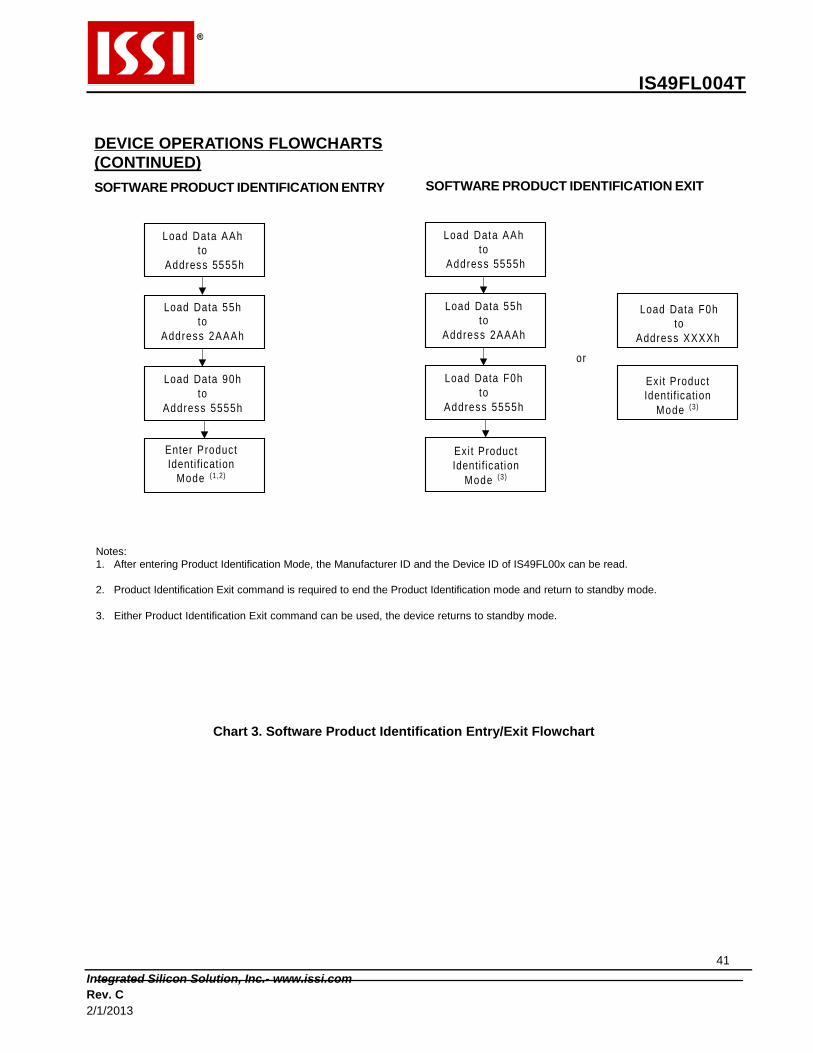
DEVICE OPERATIONS FLOWCHARTS
(CONTINUED)
SOFTWARE PRODUCT IDENTIFICATION ENTRY
SOFTWARE PRODUCT IDENTIFICATION EXIT
Load Data AAh
to
Address 5555h
Load Data AAh
to
Address 5555h
Load Data 55h
to
Address 2AAAh
Load Data 90h
to
Address 5555h
Load Data 55h
to
Address 2AAAh
Load Data F0h
to
Address 5555h
Load Data F0h
to
Address XXXXh
or
Exi t Product
Identif ication
Mode (3)
Enter Product
Identif ication
Mode (1,2)
Exi t Product
Identif ication
Mode (3)
Notes:
1. After entering Product Identification Mode, the Manufacturer ID and the Device ID of IS49FL00x can be read.
2. Product Identification Exit command is required to end the Product Identification mode and return to standby mode.
3. Either Product Identification Exit command can be used, the device returns to standby mode.
Chart 3. Software Product Identification Entry/Exit Flowchart

IS49FL004T
Integrated Silicon Solution, Inc.- www.issi.com
Rev. C
2/1/2013
42
ABSOLUTE MAXIMUM RATINGS (1)
Temperature Under Bias -55oC to +125oC
Storage Temperature -65oC to +150oC
Surface Mount Lead Soldering Temperature
Standard Package 240oC 3 Seconds
Lead-free Package 260oC 3 Seconds
Input Voltage with Respect to Ground on All Pins (2)
-0.5 V to VCC + 0.5 V
All Output Voltage with Respect to Ground -0.5 V to VCC + 0.5 V
VCC (2) -0.5 V to +6.0 V
Notes:
1. Stresses under those listed in “Absolute Maximum Ratings” may cause permanent damage
to the device. This is a stress rating only. The functional operation of the device or any other
conditions under those indicated in the operational sections of this specification is not
implied. Exposure to absolute maximum rating condition for extended periods may affected
device reliability.
2. Maximum DC voltage on input or I/O pins are +6.25 V. During voltage transitioning period, input or I/O pins may overshoot to VCC + 2.0 V for a period of time up to 20 ns. Minimum
DC voltage on input or I/O pins are -0.5 V. During voltage transitioning period, input or I/O pins may undershoot GND to -2.0 V for a period of time up to 20 ns.
DC AND AC OPERATING RANGE
Part Number IS49FL002 IS49FL004
Operating Temperature
0o C to 85oC
0o C to 85oC
Vcc Power Supply
3.0 V - 3.6 V
3.0 V - 3.6 V

IS49FL004T
Integrated Silicon Solution, Inc.- www.issi.com
Rev. C
2/1/2013
43
CC
DC CHARACTERISTICS
Symbol Parameter Condition Min Typ Max Units
II
Input Leakage Current for IC,
ID[3:0] pins
VIN = 0 V to VCC, VCC = VCC max
100
A
ILI Input Leakage Current VIN = 0 V to VCC, VCC = VCC max
A
ILO Output Leakage Current VI/O = 0 V to VCC, VCC = VCC max A
ISB
Standby VCC Current
(FWH/LPC Mode)
FWH4 or LFRAME# = VIH,
f = 33 MHz; VCC = VCC max
500
A
IRY
Ready Mode VCC Current
(FWH/LPC Mode)
FWH4 or LFRAME# = VIL,
f = 33 MHz; IOUT = 0 mA,
VCC = VCC max
10
mA
ICC1
VCC Active Read Current
(FWH/LPC Mode)
FWH4 or LFRAME# = VIL,
f = 33 MHz; IOUT = 0 mA,
VCC = VCC max
2
15
mA
ICC2 (1) VCC Program/Erase Current 7 20 mA
VIL Input Low Voltage -0.5 0.3 VCC V
VIH Input High Voltage 0.7 VCC VCC + 0.5 V
VOL Output Low Voltage IOL = 2.0 mA, VCC = VCC min 0.1 VCC V
VOH Output High Voltage IOH = -100 mA, VCC = VCC min 0.9 VCC V
Note: 1. Characterized but not 100% tested.
AC CHARACTERISTICS
PIN IMPEDANCE (V = 3.3 V, f = 1 MHz, T = 25°C )
Typ Max Units Conditions
CI/O (1)
I/O Pin Capacitance
12
pF
VI/O = 0 V
CIN (1)
Input Capacitance
12
pF
VIN = 0 V
LPIN (2)
Pin Inductance
20
nH
Notes:
1. These parameters are characterized but not 100% tested.
2. Refer to PCI specification.

IS49FL004T
Integrated Silicon Solution, Inc.- www.issi.com
Rev. C
2/1/2013
44
AC CHARACTERISTICS (CONTINUED)
FWH/LPC INTERFACE AC INPUT/OUTPUT CHARACTERISTICS
Symbol Parameter Condition Min Max Units
IOH (AC)
Switching current
high
0 < VOUT < 0.3 VCC
-12 VCC
mA
0.3 VCC < VOUT < 0.9 VCC
-17.1 (VCC - VOUT)
mA
0.7 VCC < VOUT < VCC Equation C (1)
(Test point)
VOUT = 0.7 VCC
-32 VCC
mA
IOL (AC)
Switching current low
VCC > VOUT > 0.6 VCC
16 VCC
mA
0.6 VCC > VOUT > 0.1 VCC
-17.1 (VCC - VOUT)
mA
0.18 VCC > VOUT > 0 Equation D (1)
(Test point)
VOUT = 0.18 VCC
38 VCC
mA
ICL
Low clamp current
-3 < VIN < -1
-25 + (VIN + 1) / 0.015
mA
ICH
High clamp current
VCC + 4 > VIN > VCC + 1
25 + (VIN - VCC - 1) /
0.015
mA
slewr (2)
Output rise slew rate
0.2 VCC - 0.6 VCC load
1
4
V/ns
slewf (2)
Output fall slew rate
0.6 VCC - 0.2 VCC load
1
4
V/ns
Notes:
1. See PCI specification.
2. PCI specification output load is used.
FWH/LPC INTERFACE CLOCK CHARACTERISTICS
Symbol Parameter Min Max Units
tCYC
Clock Cycle Time
30
ns
tHIGH
Clock High Time
11
ns
tLOW
Clock Low Time
11
ns
Clock Slew Rate
1
4
V/ns
INIT# or RST# Slew Rate
50
mV/ns

IS49FL004T
Integrated Silicon Solution, Inc.- www.issi.com
Rev. C
2/1/2013
45
AC CHARACTERISTICS (CONTINUED)
FWH/LPC INTERFACE CLOCK WAVEFORM
0.5 V C C
0.4 V C C
0.3 V C C
tHIG H
tC Y C
tL O W
0.6 V C C
(min imum)
0.2 V C C
FWH/LPC INTERFACE MEASUREMENT CONDITION PARAMETERS
Symbol Value Units
VTH1
0.6 VCC
V
VTL1
0.2 VCC
V
VTEST
0.4 VCC
V
VMAX1
0.4 VCC
V
Input Signal Edge Rate
1 V/ns
Note: 1. The input test environment is done with 0.1 VCC of overdrive over VIH and VIL. Timing parameters must
be met with no more overdrive that this. VMAX specifies the maximum peak-to-peak waveform allowed
for measuring input timing. Production testing may use different voltage values, but must correlate
results back to these parameter.
FWH/LPC MEMORY READ/WRITE OPERATIONS CHARACTERISTICS
Symbol Parameter Min Max Units
TCYC
Clock Cycle Time
30
ns
TSU
Input Set Up Time
7
ns
TH
Input Hold Time
0
ns
TVAL
Clock to Data Out
2
11
ns
TON
Clock to Active Time (float to active delay)
2
ns
TOFF
Clock to Inactive Time (active to float delay)
28
ns

IS49FL004T
Integrated Silicon Solution, Inc.- www.issi.com
Rev. C
2/1/2013
46
AC CHARACTERISTICS (CONTINUED)
FWH/LPC INPUT TIMING PARAMETERS
CLK
FWH[3:0] or
LAD[3:0] (Val id Input Data)
tS U
INPUT VALI D
V T ES T
tH
V T H
V T L
V
M A X
FWH/LPC OUTPUT TIMING PARAMETERS
CLK
FWH[3:0] or
LAD[3:0] (Val id Outpu t Data)
FWH[3:0] or
LAD[3:0] (Float Outpu t Data)
V
T ES T
tVAL
tO F F
tO N
V T H
V
TL

IS49FL004T
Integrated Silicon Solution, Inc.- www.issi.com
Rev. C
2/1/2013
47
AC CHARACTERISTICS (CONTINUED)
FWH/LPC RESET OPERATION CHARACTERISTICS
Symbol Parameter Min Max Units
TPRST
Reset Active Time to VCC Stable 1 ms
TKRST
Reset Active Time to Clock Stable 100 s
TRSTP
Reset Pulse Width 100 ns
TRSTF
Reset Active to Output Float Delay 50 ns
T (1)
RST
Reset Inactive Time to Input Active 1 s
Note: 1. There will be a 10 µs reset latency if a reset procedure is performed during a programming or erase
operation.
FWH/LPC RESET AC WAVEFORMS
V C C
T P R S T
CLK
RST#/INIT#
FWH[3:0] or
LAD[3:0]
FWH 4 or
LF RAME #
T
K R S T
T
R ST F
T
R S T P
T
R S T
A/A MUX MODE INPUT TEST MEASUREMENT CONDITION PARAMETERS
3.0 V
Input
0.0 V
1.5 V
A C
Measuremen t
Level
A/A MUX MODE TEST LOAD CONDITION
T O T E ST E R
T O D U T
C
L
30 pF

IS49FL004T
Integrated Silicon Solution, Inc.- www.issi.com
Rev. C
2/1/2013
48
AC CHARACTERISTICS (CONTINUED)
A/A MUX MODE READ OPERATIONS CHARACTERISTICS
Symbol
Parameter
Min
Max
Units
tRC
Read Cycle Time 270 ns
tACC
Address to Output Delay 120 ns
tRST
RST# High to Row Address Set-up Time 1 ms
tAS
R/C# Address Set-up Time 45 ns
tAH
R/C# Address Hold Time 45 ns
tOE
OE# to Output Delay 50 ns
tDF
OE# to Output High Z 0 30 ns
tOH
Output Hold from OE# or Address, whichever occured first 0 ns
tVCS
VCC Set-up Time 50 s
A/A MUX MODE READ OPERATIONS AC WAVEFORMS
RST#
A D D R E S S
tR S T
R OW ADD RES S
tR C
COLUMN ADDRESS
R/C#
O E #
W E #
tA S tA H tA S tA H
tAC C
tO E tD F
tO H
OU TPU T
V CC
tVC S
HIGH Z O UT PUT
VALID

IS49FL004T
Integrated Silicon Solution, Inc.- www.issi.com
Rev. C
2/1/2013
49
AC CHARACTERISTICS (CONTINUED) A/A MUX MODE WRITE (PROGRAM/ERASE) OPERATIONS CHARACTERISTICS
Symbol Parameter Min Max Units
tRST RST# High to Row Address Set-up Time 1 ms
tAS R/C# Address Set-up Time 50 ns
tAH R/C# Address Hold Time 50 ns
tCWH R/C# to WE# High Time 50 ns
tOES OE# High Set-up Time 20 ns
tOEH OE# High Hold Time 20 ns
tDS Data Set-up Time 50 ns
tDH Data Hold Time 5 ns
tWP Write Pulse Width 100 ns
tWPH Write Pulse Width High 100 ns
tBP Byte Programming Time 40 s
tEC Chip, Sector or Block Erase Cycle Time 80 ms
tVCS VCC Set-up Time 50 s
A/A MUX MODE WRITE OPERATIONS AC WAVEFORMS
RST# tR S T
tR C
A D D R E S S R OW ADD RES S COLUMN ADDRESS
R/C#
O E #
W E #
tVC S
tA S tA H tA S tA H
tC W H tO E H
tO E S
tD S tD H
OU TPU T HIGH Z
INPUT
DAT A
V CC

IS49FL004T
Integrated Silicon Solution, Inc.- www.issi.com
Rev. C
2/1/2013
50
DAT A
t
AC CHARACTERISTICS (CONTINUED)
A/A MUX MODE BYTE PROGRAM OPERATIONS AC WAVEFORMS
A D D R E S S
4-Byte Program Command
5555
2AAA
5555 B YTE ADDRESS
R/C#
W E #
tC W H
tW P
tW P H
B P
O E #
tD S
tD H
DA TA A A 5 5 A0 INPUT
VALID
DAT A
A/A MUX MODE CHIP ERASE OPERATIONS AC WAVEFORMS
6-Byte Chip Erase Command
A D D R E S S
5555
2AAA
5555
5555
2AAA
5555
R/C#
W E #
tC W H
tW P tW P H tE C
O E #
tD S
tD H
DATA IN A A 55 80 A A 55 10

IS49FL004T
Integrated Silicon Solution, Inc.- www.issi.com
Rev. C
2/1/2013
51
AC CHARACTERISTICS (CONTINUED)
A/A MUX MODE SECTOR/BLOCK ERASE OPERATIONS AC WAVEFORMS
6-Byte Block Erase Command
A D D R E S S
R/C#
5555
2AAA
5555
5555
2AAA
SECT O R O R
BL O CK ADDRES S
W E #
tC W H
tW P tW P H tE C
O E #
tD S
t
D H
DATA IN AA 55 8 0 A A 55 30/50
A/A MUX MODE TOGGLE BIT AC WAVEFORMS
ADDRES S R O W CO L UM N
R/C#
W E #
O E #
I /O6
tO E H
D
tO E
D
Note: 1. Toggling OE# will operate Toggle Bit.
2. I/O6 may start and end from “1” or “0” in random.

IS49FL004T
Integrated Silicon Solution, Inc.- www.issi.com
Rev. C
2/1/2013
52
AC CHARACTERISTICS (CONTINUED)
A/A MUX MODE DATA# POLLING AC WAVEFORMS
ADDRES S R O W CO L UM N
R/C#
W E #
O E #
I /O7
tO E H
D
tO E
D#
D# D# D
Note: Toggling OE# will operate Data# Polling.
PROGRAM/ERASE PERFORMANCE
Parameter Unit Typ Max Remarks
Sector/Block Erase Time
ms
50
80
From writing erase command to erase completion
Chip Erase Time
ms
50
80
From writing erase command to erase completion
Byte Programming Time
s
25
40
Excludes the time of four-cycle program command
execution
Note: These parameters are characterized but not 100% tested.
RELIABILITY CHARACTERISTICS (1)
Parameter Min Typ Unit Test Method
Endurance
100,000 (2)
Cycles
JEDEC Standard A117
Data Retention
20
Years
JEDEC Standard A103
ESD - Human Body Model
2,000
>4,000
Volts
JEDEC Standard A114
ESD - Machine Model
200
>400
Volts
JEDEC Standard A115
Latch-Up
100 + ICC1
mA
JEDEC Standard 78
Notes: 1. These parameters are characterized but not 100% tested.
2. Preliminary specification only and will be formalized after cycling qualification test.

IS49FL004T
Integrated Silicon Solution, Inc.- www.issi.com
Rev. C
2/1/2013
53
PACKAGE TYPE INFORMATION
32V 32-Pin Thin Small Outline Package (VSOP - 8 mm x 14 mm)( measure in millimeters)
Pin 1 I.D.
1.05
0.95
0.27
0.17
8 .10
7 .90
0.50
B S C
12.50
12.30
14.20
13.80
0.15
0.05
1.20
M A X
0.25
0.20
0 ° 0.10
5 ° 0 .70
0 .50
32J 32-Pin Plastic Leaded Chip Carrier (measured in millimeters)
12.57
12.32
11.51
11.35
15.11
14.86
14.05
Pin 1 I .D.
3 .56
3 .18
2 .41
1 .93
0 .74X30 °
13.89 SEAT ING
PLAN E
0.81
0.66
1.27 Typ.
0.53
0 .33
13.46
12.45

IS49FL004T
Integrated Silicon Solution, Inc.- www.issi.com
Rev. C
2/1/2013
54
TOP VIEW SIDE VIEW
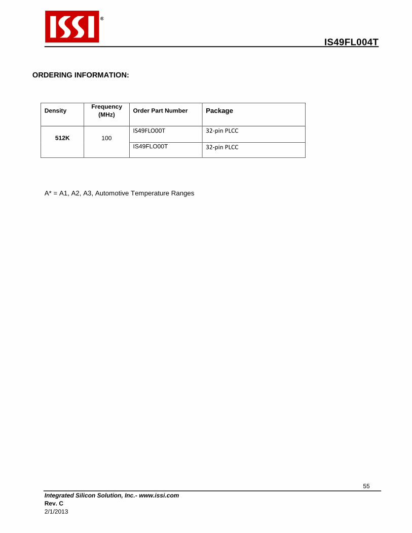
IS49FL004T
Integrated Silicon Solution, Inc.- www.issi.com
Rev. C
2/1/2013
55
ORDERING INFORMATION:
Density Frequency
(MHz) Order Part Number Package
512K 100
IS49FLO00T 32-pin PLCC
IS49FLO00T 32-pin PLCC
A* = A1, A2, A3, Automotive Temperature Ranges