IS31LT3505 Constant Current, Step-Up LED Driver · PDF fileIS31LT3505 Constant Current,...
5
IS31LT3505 Constant Current, Step-Up LED Driver Evaluation Board Guide Integrated Silicon Solution, Inc. – www.issi.com 1 R2, 6/12/2012 Description IS31LT3505 is a constant current boost converter with an internal NMOS. The device topology allows for series type connections of white LEDs, with identical output currents for each channel. This allows for consistent, uniform lighting output and it also ensures that any linked system components receive their respective voltage source(s). The LED current can be adjusted by tuning an external resistor. Dimming of the panel is achieved through Pulse-width-modulation (PWM) or through a DC voltage signal. The driver features a 1MHz switching frequency. Feedback voltage is set at 0.3V to minimize power drain. Safety features of the device include Over-voltage Protection, Over-temperature Protection, and Open-circuit LED protection. This ensures that the chip will maintain a maximum level of reliability for the overall system, even under abnormal situations such as when no load is present. IS31LT3505 may be used in a versatile array of general lighting applications. Features Supply Voltage: 6V to 30V Efficiency: 90% (typical) PWM or DC Voltage Dimming Control 1.0MHz Switching Frequency 35V High-powered Internal NMOS Open-circuit LED Protection Over-temperature, voltage Protection Package: MSOP-10 Recommended Equipment 30VDC Supply LED panel/array (1W LED, 9 LEDs in series) Multi-meter Quick Start Figure 1: Picture of IS31LT3505-SLS2-EBDC Recommended I/O Ratings Input Voltage: 10-25VDC Output Current: 4-9 LEDs (series) - 350mA/Ch. Note: The input voltage must be 10%*V OUT lower than the output voltage (∑V F ) and input average current should be ≤1000mA. Absolute Maximum Ratings Input voltage ≤ 30VDC Caution: Do not exceed the conditions listed above, otherwise the board will be damaged. Procedure Follow the steps listed below to verify board operation. Caution: Do not turn on the power supply until all connections are completed. 1) Connect the negative terminal of the power supply to the GND pin and the positive terminal to the V IN pin. 2) Connect the negative end of the LED panel (LED arrays) to the LED- terminal. 3) Connect the positive end of the LED panel (LED arrays) to the LED+ terminal. 4) Turn on the power supply and the LED panel (LED arrays) will turn on. Order information Part Number Description Package IS31LT3505-SLS2-EBDC 6-30V Input Voltage, <1000mA. Output: V IN /0.9 MSOP-10 Table 1: Ordering Information for IS31LT3505 Evaluation Board For information about ordering, deliveries, and pricing, please contact ISSI at [email protected] or (408)969-6600.
Transcript of IS31LT3505 Constant Current, Step-Up LED Driver · PDF fileIS31LT3505 Constant Current,...
IS31LT3505 Constant Current, Step-Up LED Driver Evaluation Board Guide
Integrated Silicon Solution, Inc. – www.issi.com 1 R2, 6/12/2012
Description
IS31LT3505 is a constant current boost converter with an internal NMOS. The device topology allows for series type connections of white LEDs, with identical output currents for each channel. This allows for consistent, uniform lighting output and it also ensures that any linked system components receive their respective voltage source(s). The LED current can be adjusted by tuning an external resistor. Dimming of the panel is achieved through Pulse-width-modulation (PWM) or through a DC voltage signal. The driver features a 1MHz switching frequency. Feedback voltage is set at 0.3V to minimize power drain. Safety features of the device include Over-voltage Protection, Over-temperature Protection, and Open-circuit LED protection. This ensures that the chip will maintain a maximum level of reliability for the overall system, even under abnormal situations such as when no load is present. IS31LT3505 may be used in a versatile array of general lighting applications.
Features
Supply Voltage: 6V to 30V
Efficiency: 90% (typical)
PWM or DC Voltage Dimming Control
1.0MHz Switching Frequency
35V High-powered Internal NMOS
Open-circuit LED Protection
Over-temperature, voltage Protection
Package: MSOP-10
Recommended Equipment
30VDC Supply
LED panel/array (1W LED, 9 LEDs in series)
Multi-meter
Quick Start
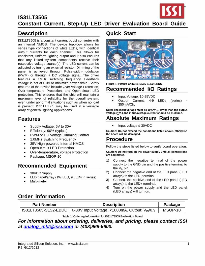
Figure 1: Picture of IS31LT3505-SLS2-EBDC
Recommended I/O Ratings
Input Voltage: 10-25VDC
Output Current: 4-9 LEDs (series) - 350mA/Ch.
Note: The input voltage must be 10%*VOUT lower than the output voltage (∑VF) and input average current should be ≤1000mA.
Absolute Maximum Ratings
Input voltage ≤ 30VDC
Caution: Do not exceed the conditions listed above, otherwise the board will be damaged.
Procedure
Follow the steps listed below to verify board operation.
Caution: Do not turn on the power supply until all connections are completed.
1) Connect the negative terminal of the power supply to the GND pin and the positive terminal to the VIN pin.
2) Connect the negative end of the LED panel (LED arrays) to the LED- terminal.
3) Connect the positive end of the LED panel (LED arrays) to the LED+ terminal.
4) Turn on the power supply and the LED panel (LED arrays) will turn on.
Order information
Part Number Description Package
IS31LT3505-SLS2-EBDC 6-30V Input Voltage, <1000mA. Output: VIN/0.9 MSOP-10
Table 1: Ordering Information for IS31LT3505 Evaluation Board
For information about ordering, deliveries, and pricing, please contact ISSI at [email protected] or (408)969-6600.
IS31LT3505 Constant Current, Step-Up LED Driver Evaluation Board Guide
Integrated Silicon Solution, Inc. – www.issi.com 2 R2, 6/12/2012
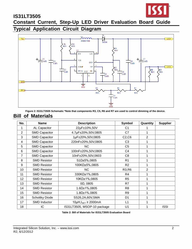
Typical Application Circuit Diagram
Figure 2: IS31LT3505 Schematic *Note that components R3, C5, R6 and R7 are used to control dimming of the device.
Bill of Materials
No. Name Description Symbol Quantity Supplier
1 AL Capacitor 22μF±10%,50V C1 1
2 SMD Capacitor 4.7μF±20%,50V,0805 C7 1
3 SMD Capacitor 1μF±20%,50V,0805 C2,C6 2
4 SMD Capacitor 220nF±20%,50V,0805 C3 1
5 SMD Capacitor NC C5 1
6 SMD Capacitor 100nF±20%,50V,0805 C4 1
7 SMD Capacitor 10nF±20%,50V,0603 C8 1
8 SMD Resistor 51Ω±5%,0805 R1 1
9 SMD Resistor 100KΩ±5%,0805 R2 1
10 SMD Resistor NC R3,R6 2
11 SMD Resistor 330KΩ±1%,0805 R4 1
12 SMD Resistor 10KΩ±1%,0805 R5 1
13 SMD Resistor 0Ω, 0805 R7 1
14 SMD Resistor 1.6Ω±1%,0805 R8 1
15 SMD Resistor 1.8Ω±1%,0805 R9 1
16 Schottky Diode SS26,2A,60V,SMA D1 1
17 SMD Inductor 10μH,ISET ≥ 2000mA L1 1
18 IC IS31LT3505, MSOP-10 package U1 1 ISSI
Table 2: Bill of Materials for IS31LT3505 Evaluation Board
IS31LT3505 Constant Current, Step-Up LED Driver Evaluation Board Guide
Integrated Silicon Solution, Inc. – www.issi.com 3 R2, 6/12/2012
Device Operation
Component Selection
The component selection is very important. They have a significant effect on the operating state of the demo board. The output capacitor must be a low ESR capacitor so as to minimize it’s affect on the line regulation and load regulation. Please read the datasheet carefully to get more information about the component selection.
LED Current Control The IS31LT3505 regulates the LED current by setting the external resistor connecting to feedback and ground. The internal feedback reference voltage is 0.3V (Typical) The LED current can be set from the Formula (1) easily. ILED = VFB/RSET Where: RSET=R8//R9 In order to have an accurate LED current, precision resistors must be used (1% is recommended).
PCB layout consideration As for all switching power supplies, especially those providing high current and using high switching frequencies, layout is an important design step. If layout is not carefully done, the regulator could show instability as well as EMI problems.
Wide traces should be used for connection of the high current loop.
When laying out signal ground (pin 5), it is recommended to use the traces separate from power ground (pin1) traces and connect them together at the input capacitor negative terminal or the large ground plane that will avoid the signal ground shift. Pin 3 GND must be connected to signal ground(pin 5). Both of signal and power ground should be as wide as possible. Other components ground must be connected to signal ground. Especially the RSET ground to signal ground (pin 5) connection should be as short as possible to have an accurate LED current.
The capacitor CVDD and CVP should be placed as close as possible to VDD and VP pin for good filtering.
LX pin is a fast switching node. The inductor and diode should be placed as close as possible to the switch pin and the connection between this pin to the inductor and the schottky diode should be kept as short and wide as possible. Avoid other traces cross and routing too long in parallel with this node to minimum the noise coupling into these traces.
The feedback network (FB, OVP) should be as short as possible and routed away from the inductor, the schottky diode and LX pin. The feedback pin and feedback network should be shielded with a ground plane or trace to minimize noise coupling into this circuit.
The thermal pad on the back of package must be soldered to the large ground plane for ideal power dissipation.
IS31LT3505 Constant Current, Step-Up LED Driver Evaluation Board Guide
Integrated Silicon Solution, Inc. – www.issi.com 4 R2, 6/12/2012
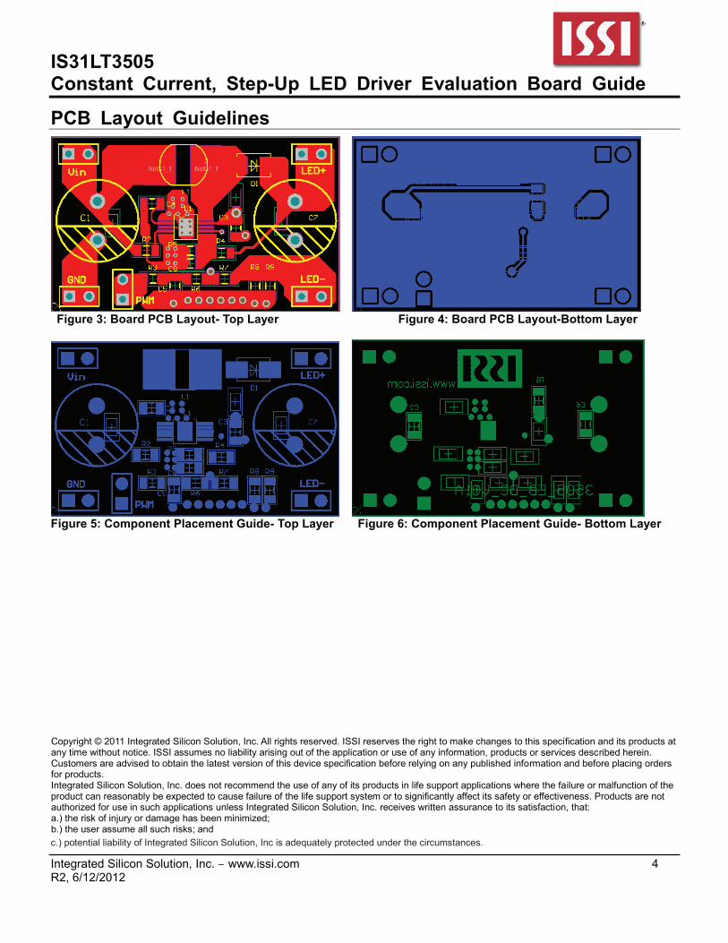
PCB Layout Guidelines
Figure 3: Board PCB Layout- Top Layer Figure 4: Board PCB Layout-Bottom Layer
Figure 5: Component Placement Guide- Top Layer Figure 6: Component Placement Guide- Bottom Layer
Copyright © 2011 Integrated Silicon Solution, Inc. All rights reserved. ISSI reserves the right to make changes to this specification and its products at any time without notice. ISSI assumes no liability arising out of the application or use of any information, products or services described herein. Customers are advised to obtain the latest version of this device specification before relying on any published information and before placing orders for products. Integrated Silicon Solution, Inc. does not recommend the use of any of its products in life support applications where the failure or malfunction of the product can reasonably be expected to cause failure of the life support system or to significantly affect its safety or effectiveness. Products are not authorized for use in such applications unless Integrated Silicon Solution, Inc. receives written assurance to its satisfaction, that: a.) the risk of injury or damage has been minimized; b.) the user assume all such risks; and c.) potential liability of Integrated Silicon Solution, Inc is adequately protected under the circumstances.