IS 7576 (1974): Bunched enamelled copper …IS : 7576 - 1974 1. SCOPE 1.1 This standard specifies...
23
Disclosure to Promote the Right To Information Whereas the Parliament of India has set out to provide a practical regime of right to information for citizens to secure access to information under the control of public authorities, in order to promote transparency and accountability in the working of every public authority, and whereas the attached publication of the Bureau of Indian Standards is of particular interest to the public, particularly disadvantaged communities and those engaged in the pursuit of education and knowledge, the attached public safety standard is made available to promote the timely dissemination of this information in an accurate manner to the public. इंटरनेट मानक “!ान $ एक न’ भारत का +नम-ण” Satyanarayan Gangaram Pitroda “Invent a New India Using Knowledge” “प0रा1 को छोड न’ 5 तरफ” Jawaharlal Nehru “Step Out From the Old to the New” “जान1 का अ+धकार, जी1 का अ+धकार” Mazdoor Kisan Shakti Sangathan “The Right to Information, The Right to Live” “!ान एक ऐसा खजाना > जो कभी च0राया नहB जा सकता ह ै” Bhartṛhari—Nītiśatakam “Knowledge is such a treasure which cannot be stolen” IS 7576 (1974): Bunched enamelled copper conductors with silk covering [ETD 33: Winding Wire]
Transcript of IS 7576 (1974): Bunched enamelled copper …IS : 7576 - 1974 1. SCOPE 1.1 This standard specifies...

Disclosure to Promote the Right To Information
Whereas the Parliament of India has set out to provide a practical regime of right to information for citizens to secure access to information under the control of public authorities, in order to promote transparency and accountability in the working of every public authority, and whereas the attached publication of the Bureau of Indian Standards is of particular interest to the public, particularly disadvantaged communities and those engaged in the pursuit of education and knowledge, the attached public safety standard is made available to promote the timely dissemination of this information in an accurate manner to the public.
इंटरनेट मानक
“!ान $ एक न' भारत का +नम-ण”Satyanarayan Gangaram Pitroda
“Invent a New India Using Knowledge”
“प0रा1 को छोड न' 5 तरफ”Jawaharlal Nehru
“Step Out From the Old to the New”
“जान1 का अ+धकार, जी1 का अ+धकार”Mazdoor Kisan Shakti Sangathan
“The Right to Information, The Right to Live”
“!ान एक ऐसा खजाना > जो कभी च0राया नहB जा सकता है”Bhartṛhari—Nītiśatakam
“Knowledge is such a treasure which cannot be stolen”
“Invent a New India Using Knowledge”
है”ह”ह
IS 7576 (1974): Bunched enamelled copper conductors withsilk covering [ETD 33: Winding Wire]


I6 : 7576 - 1974
Indian Standard SPECIFICATION FOR
BUNCHED ENAMELLED COPPER WI~RES WITH SILK COVERING
Winding Wires Sectional Committee, ETDC 33
Chairman
SHRl K. DORAISIVAMY
Members
Representing
Dr Beck b: Co (India) Ltd, Poona
SXRI S. B. BAI*.~T (Alternate to Shri. K. Doraiswamy)
A~~~~TANT DIRECTOR ELECTRICAL Naval Headquarters ENGINEERING (MATEIUAL)
ASSISTANT DI~UXTOR LOGISTIC Su~noars (TECHIVICAL) (Alternate)
SHRI G. K. BIIANDARKAR Crompton Greavcs Ltd, Bombay Snm S. V. MANEJUKM (Alima*)
SHRI C. IL BHASKAX RAO Bharat Bijlee Ltd, Bombay SHRI R. W. PRA~HAN IAltemate~
WC CDR H. S. BHATIA ’
SIIRI H. C. PANDE (Alternate) CHIEF ELECTRICAL ENGINEER
DEPUTY Ctnnv E~.ECTRICAL ENGINEER (Alternate)
DIRECTOR, CENTRAL POWIZR RE- SEARCII INSTITUTE
Dspvn DIRECTOR, CENTRAL POWI:R RESTARTS INSTITUTE (Alternate)
SHRI M. L. GAXGULY SHRX M. DEY (Alternate)
DR A. X. G~SWAMI SHRI S. KU~~AR (Alternate)
SHRI D. P. GUPTA
Directorate of Technical Development & Produc- tion (Air) (Ministry of &fence), New Delhi
Railway Board (_Ministry of Railways)
Central Water and Power Commission (Power Wing), New Delhi
Indian Cable Co Ltd, Calcutta
Bharat Heavy Electricals Ltd, Bhopal
Directorate General of Technical Development, New Delhi
SHRI K. GURURAJ.~ Bharat Electronics Ltd, Bangalore SIIRI R. SOMASEKIIARA’ (Al!ernate)
!&RI P. N. HIR~YANNAIIAH SIIRI K. N. JIIAVERI
Kirloskar Electric Co Ltd, Bangalore
SHRI kl. N. KUYAR (Alternate) 3hakti Insulated Wires Private Ltd, Bombay
(Continued on ;~a::” 2’
0 Copyright 1975
INDIAN STANDARDS INSTITUTION This publication is protected under the Indiun Copyright Act (XIV of 1957) and reproduction in whole or in part by any means except with written permission of the publisher shall be deemed to be an infringement of copyright under the said Xct
I
IS I 7576 - 1974
SHR~ R. R. JHUsrWALA SHRI A. M. GHATAK (Alternate)
Philips India Ltd, Bombay
Sxar hm -I K-I Hindustan Transmission Products, Bombay Srrnr N. R. LODH Devidayal Electronics &’ Wires Ltd, Bombay
SHRI N. P. SANGAMESWARAN (Alternate) SW’ D. R. MANOHAR National Insulated Cable Co of India Ltd, Calcutta
&RI J. S. BWAN (Aknatc) Sm S. K. MUKHERJEE National Test House, Calcutta. SHRr J. s. PAssI Directorate General of Supplies & Disposals (Ins-
SHRI J. L. CHWABRA (Ahnate) pection Wing), New Delhi
Drm G. H. PHADrcn Indian Electrical Manufacturers’ Association, Bombay
Srrru D. B. GUPTA (Alternate) &RI P. L. PRAmiAN
SHRI B. G. S-A (AZttmate) Snxu A. K. I(AIIAN Ssmr L. G. VARADARAJAN
SfiRI P. V. R.+o (Altematc) Sxuu N. SRINIVASAN,
Director (Elec tech)
Jyoti Ltd, Baroda
Asian Cables Corporation Ltd, Bombay Indii Telephone Industries Ltd, Bangalore
Director General, IS1 @k-o&o Mrmbcr)
secYeta?y
SHRI HARCHARAN S~G~K Assistant Director (Elec tech), IS1
2
IS : 7576 - I974
Indian Stmclkard SPECIFICATION FOR
BUNCHED ENAMELLED COPPER WIRES WITH SILK COVERING
0. FOREWORD
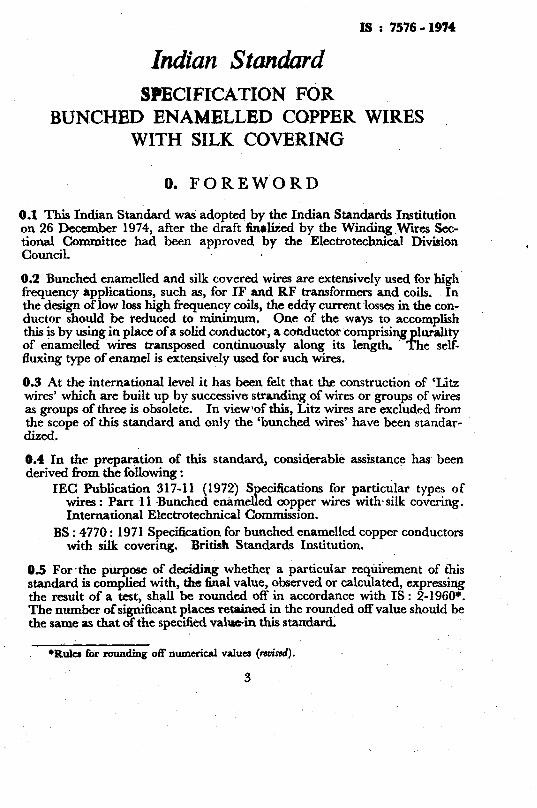
0.1 This Indian Standard was adopted by the Indian Standards Institution on 26 December 1974, after the draft finrlked by the Winding,Wires Set- tional Committee had been approved by the Electrotechnkal Division c0llnci1.
0.2 Bunched enamelled and silk covered wires are extensively used for high frequency applications, such as, for IF and RF transformers and coils. In the design of low loss high frequency coils, the eddy current losses in the con- ductor should be reduced to minimum. One of the ways to accomplish this is by using in place of a solid conductor, a conductor comprising of enamelled wires transposed continuously along its length. *
lh~y;ly -
fluxing type of enamel is extensively used for such wires.
0.3 At the international level it has been felt that the construction of ‘Litz wires’ which are built up by successive stranding of wires or groups of wires as groups of three is obsolete. In view$of this, Litz wires are excluded from the scope of this standard and only the ‘bunched wires’ have been standar- dized.
0.4 In the preparation of this standard, considerable assistance has been derived fkom the following :
IEC Publication 317-11 (1972) Specifications for particular types of wires : Part 11 Bunched enamelled oopper wires with.& covering. International Electrotechnical Commission.
BS : 4770 : 197 1 Specification for bunched enamelled copper conductors with silk covering. British Standards Institution.
0.5 For .the purpose of deciding whether a particdar requirement of this standard is complied with, the final value, observed or calculated, expressing the result of a test, shall be rounded off in accordance with IS : 2-1960*. The number of significant places retained in the rounded off value should be the same as that of the specified valmin thii starrdard.
*Rules for rounding off numerical values (rmiwd).
3
IS : 7576 - 1974
1. SCOPE
1.1 This standard specifies requirements and dimemionq for bunched ena- melled copper wires with silk covering normally used for high frequency a ‘cations. o!Y
The esMe&d conductor shall conform to Fine (F) covering S : 4800 (Part VT)-1968’.
1.2 The requirements of the standard are applicable to bunched wires made up of wires having conductor diameters from 0.025 to 0.071 mm.
2. TERMINOLOGY
2.0 For the purpose of this standard, the following definitions shall apply.
21 wire - The single enamelled conductor.
2.2 Conductor - The bare copper wire after the removal of the enamel film from the single wire.
2.3 Bun&cd Wire - The laid up compositi with it< textile covering.
2.4 Lay - The axial length of one complete turn of the helix formed by the bunched wire.
2.5 Toleramce that prescribed.
- The permissible divergence ~ti an actual magnitude from
2.6 Dielectric Dissipation factor (tan 8) - The tangent of the loss angle of an insulating material.
3. GENBRAL TBST CONDITIONS
3.1 Unless otherwise specified, all tests shall be carried out within a tem- perature range of 15 to 35’C and a relative humidity range of 45 to 75 per- cent. Before measurements are made, the specimens shall be precondi- tioned under these atmospheric conditions for a time sufficient to allow the wire to reach stability.
3.2 The bunched wire to be tested shall be removed from the packaging in such a way th%t the wire will not be subjected to tension or unnecessary
I bends.
3.3 Before each test discard sufficient length of wire to ensure that any damaged wire is not included in the test specimens.
3.4 Nor:a!ly all mandatory requirements for a method of test are given in the description, and diagrams are only intended to illustrate one possible arrangement for conducting the test.
*Specification for enamelled tound winding wires: Part VI Wires with s&fluxing properties.
4

IS a is6 l 1974
4.ovEBALLDlAMETER
4.1 Overall Diameter of Sk& Wire --- The maximum overall diameter and the minimum increase in diameter 01’ the single wire shall be in actor- dance with Table 1.
T-1 OVERAUBwdlGTBR OF ntE &GLE WIRE
NOM~~~~UCTOR MAx1Muu OVRRALL hhlMUM INCRRME IN
DJMETER DIAMRTRR
(1) (2) (9
0% o?ri
0.032 0440 ;g35
X:E 0.050 0462 ii% . r
0463 0.078 0+07 0.071 0.088 , 0408
Nc~ra - Bunched wires with a diameter ofsingle wire of0.07 1 mm are not recommended for neiv designs.
4.2 Nozninal OveraIl Diameter of Bunched Wim - The number of wires and the nominal overall diameter of the bunched wire when measured in accordance with Appendix A shall be in accordance with Table 2.
43.1 The figures given in Table 2 are related to the measurement on a mandrel. The real figures measured with a microscope arc approximately 8 percent lower.
4.5 Maximum Over& Diameter of Bunched wire - The maximum v&e of overall diameter, when measured on the mandrel, shall be not more than 10 percent higher than the figures given in Table 2.
5. RESISTANCE
5.1 The resistance for the preferred sizes at 20°C shall be within the limits given in Table 3 and shall be calculated as described in ARpendix C.
5.1.1 The nominal cross-sectional area calculated by the method des- cribed in Appendix D, and the nominal resistance calculated by the method described in Appendix C are given in Appendix D.
NOTE - Resistance of non-preferred sizes is given in Appendix B.
6. COVERING
6.1’ Application -The bunched enamelled copper wires shall have a covering of one or two lappings of silk.
The first lapping shall be applied to the bunched wires in a direction opposite to the twist of the bunched wire. If a second lapping is applied it shall be in the opposite direction to the 6rst lapping.
5

IS : 7576 - 1974
The covering shall be uniform in quality and each lapping shall be even and uniform.
6.2 Mudrel Winding To@ 7- The bunched wire shall be wound on a mandrel with a diameter 10 times the overall diameter given in Table 2 or Appendix B, under a tension calculated according to the following formula :
Tension in N = 65 x total nominal cross-sectional area of the conductor in mm2
In winding the wire round the mandrel, care shall be taken not to intro- duce a twist in the wire for each revolution.
The winding shall then be examined with normal vision in diffused light. The silk covering shall not open sufficiently to ex$ose clearly the enamelled wire.
Three tests shall be made,
TABLE 2 NOMINALOVKJL&L .DIAMETER OF BUNCHED WIRE (PB a)
(C&uses 4.2, 4.3 and 6.2)
NUNBaR NOMINAL OVERALL DIAMETER FOR
GUs NOMINAL CONWJCI-OR DIAMETER OF THE SINGLE WIRE
I *, \ 0.025 mm 0.032 mm O-040 mm 0.050 mm 0.063 mm
(1) (2) (3) (4) w (6)
: oyz!?5 oYY5 oYlY5 OYZO OYYO 0.105 0.125 0.150 0.180 0.215
2 0.115 0.120 0.150 0.140 0.175 0.165 0.195 0.210 0.255 0.235
8 0.135 0.165 0.200 0.240 0.290
:; 0.160 0.130 0.195 0.180 0.235 0.220 0.260 0.285 9.320 0.350 z: 0.220 0.200 0.275 0.245 0.300 0.335 0405 0.360 0.505 0.450
:; 0.245 0.270 X:E 0.375 0.415 0.455 0.505 0.565 0.630
60 0.320 0.405 0.506 0.615 0.785
100 0405 0.515 ~0.640 0.805 I*000
160 0.505 iG% zi% 1.005 1.255 250 0.625 0.820 1.015 1.245 l-550
NOTE 1 - The number of wires is taken from the R series of pr&rrcd numbers, and rounded for technical reasons.
NOTE 2 -Above the line, normally one silk layer is applied and below the line, a double silk layer is applied.
Nora 3 -The overall diimeter is calculated according to the method given in Appendix A.
NOTE 4- Overall diameters Ibr other commonly usal non-preferlEd sires arc given in Appendix B.
6

NUMBER
Iv%
(1)
-J s 2 8
:20 20
%3
40
1z :fi
TABLE 3 lUSI3TANCE OF THE BUNCHED, WIRE m fbE3) (Che 5.1)
h3lSTANCROP BUNCHEDWIRE POR NOMINAL CONDUCTOR DLUETER OF SINOLE WIRE
A
O-025 mm 0.032 mm O+%O mm O-050 mm 0.063 mm ’
’ ~Min Max ’ ’ Min Max ’ ’ Min Max ’ ’ Min Max ’ r Min
(2) (3) (4) (5)
Q/m Q/m Q/m b/m
(6)
Q/m
(7)
Q/m
IO.18 13-97 6.290 8.310 ’ 4.070 5.226 7,638 10.48 4,718 6.232 3-053 3.919 6,110 8.562 3.774 4.986 2442 3.135 5.092 6.985 3.145 4.155 2.035 2.613 3.819 5-239 2.359 3.116 l-526 l-960
3.055
::Z 1.222 0.955
X:CZ
00’:~’ 01122
4.191 3.493 Z-096 1.676 l-349
1,887 1.573 o-944 o-755 o-590
2.493
::z 0.977 O-802
l-221 1.018 0.611
8:Z
1.568 o-790 O-985 0.583 b306 O-659 0.82 1 0.429 0:784 0.395 0.493 O-252 O-627 O-316 o-394 o-201 0,505 0.247 o-317 o-157
l-079 0.719 O-432 O-270 o-173
0.472 0.315
<OS189 0.118 o-075 5
0642
E! . O-160 0.103
o-305 0.204 0.122 0.076 3 OG46 8
0404
:::?I 0.101 O-064 6
(8)
Q/m
::zi 1.581 i-317 0.988
0,198 0.132 0.079 0 o-049 4 0.031 6
(9) (10)
Q/m Q/m
3.284 1.678 2463 1.258 l-970 1.007 1.642 0.839 I.232 0.629
8% 0:101 0*063 4 0*040 6
0.126 1 0.083 9 O-050 3 O-031 5 oao 1
2.050 l-537 l-230
;:g
O-615 0,512 o-307 0.246 o* 198
O-158 R 0*106 . .
X’Eb G! 01025 3 3

IS : 7576 g-1974
7. DIELECTRIC DISSIPATION FACTOR
7.1 The bunched wire shall be tested by the method described in 5.13 of IS : 4800 (Part III)-1968* immediately after conditioning for 24 hours at a relative-humidity 91 to 95 percent and at a temperature of 20 to 30°C.
76.1 The dielectric dissipation factor at approximately 1 MHz shall not exceed 300 x 10-o.
8. SOLDER TEST
8.1 The bunched wire shall be tested by the method described in 5.14 of IS : 4800 (Part III)-1968*.
Temperature of the solder bath shall be 375 f 5°C. The immersion time shall be that specified in Table 4. The silk covering shall be removed.
On completion of the test, the solder shall have penetrated the .whole of the bunch and the outside shall have a smooth -coating with evidence of effective solder coating.
T-4 IMMERSION TIME IN SOLDBB BATH
NOMDL~L CROSS-SECTIONALA~EA OF THE BUNCHED WIRE
< L , Over UD to and
(1) mms
Ix&ding (2)
mm?
0.0s 0.08 0.125
0.125 0.2 8:;
;:; ;:8” 0.8 -
hMERSION
TIME
9. LENGTH OF -LAY
9.1 The length of lay shall not exceed 60 mm.
le. PAGEING AND MARKING
10.1 The bunched wire shall be wound evenly and compactly on reels complying with IS : 482-1968t. Each reel shall contain not more than two lengths of bunched wire.
+Spccification for enamelled round winding wires: Part III Methods of tests. tspeoification for reels for covered, round electrical winding wires (second rcvisian).
8
IS : 7576 - 1974
19.2 The label which is to be securely attached to the reel shall have the following information :
a) A reference to this Indian Standard, for example ‘Ref IS 7576’ b) Manufacturer’s name or trade-mark; / C) Type of enamel, that is, with self-fluxing properties; d) Number of wires and diameter of wire; and e) Weight of wire (gross and net).
10.2.1 The label may also be marked with the ISI Certification Mark. NOTE -The use of the IS1 Certification Mark is governed by the provisions of the
Indian Standards Institution (Certification Marks) Act, and the Rules and Regulations made thereunder. The IS1 mark on products covered by an Indian Standard conveys the assurance that they have been produced to comply with the requirements of that standard, under a well-defined system of inspection, testing and quality control, which is devised and supervised by IS1 and operated by the producer. IS1 marked products are also continuously checked by IS1 for conformity to that standard as a further safe- guard. Details of conditions under which a licence for the use of the IS1 Certification Mark may be granted to manufacturers or processors, may be obtained from the Indian Standards Institution.
11. SAMPLING
11.1 A recommendatorv sampling plan aild criteria t,r acceptance of lot are given in Appendix l?.
APPENDIX A
[Chuse 4.2 and Table 2 (Vote 3) ]
CALCULATION AND MEASUREMENT OF OVERALL DIAMETER OF BUNCHED WIRE
A-l. CALCULATION OF THE NOMINAL OVERALL DIAMETER
A-l .l The nominal overall diameter of the bunched wire has been calculated with the following formula :
D = pddii + the increase caused by the silk covering
where D = nominal bunched wire diameter,
p = the packing factor (see Table 5),
11 L= number of single wires, and
d = nominal overall diameter of the single wire (see Note) (see Table 6).

TAB&E 5 PACKING FACTOBk
(Clwsc A-1.1)
NUMBBROFWIRES PACK~NO @AUTQR (1) (2)
From “7 to.6 1.25 1.15
From 1: to 12 1.25 1.26
From zi to 400 1.27 1.28
N--Nominal overall diameter of! the single wire is the nominal conductor diii meter plus 2/S of the 1968’.
maximum lncre.aae of Fine wires according’to IS : 4800 (Part II)- The nominal overall diameter af the silk covered bunched enamelled conductors
is the nominal overall diameter of the bunched enamelled conductors plus the increase in dieter caused by the silk covering (se+ table below) :
&nainal Oosrall Dicun&r qfths Bunched Etumalied Candwtors
I L
covering
(11
Over
(2) mm
Upto and’ Including
(3) mm
Single silk o-450 * x’%
Double silk O%OO 1.000 l+OO
Increase in I$amtor Cawed by silk coveiing
(4) mm
o*oso to 0.035 0.035 to O-040
0.060 to o-070 0.070 to 0.080
The single silk uwerln is recommended for bunched enamelled conductors of overall diameters up to and m *CR ding 0.600 mm.
TABLE 6 lXLtXJUT&D NOMINAL OVERALL DIAMETER OF SING= WIRE
(&ure A-l. 1)
’ N”-YL%EwR NOMNAL OVERALL
DLNETER (1) (2)
mm mm
X:E$ o-029 0.037 4
0.040 o-047 0.050 O-058 a063 o-073 O*Ofl o-082
. *Specification for enamelled round winding wires: Part II Maximum overall diameters.
10

IS : 7576 - 1974
A-2. MBASmm, OF OVBRALL DIAMBTER
A-2.1 Gemad - The method indicated below does not ive accurate valuesfor use in practice but only an approtimation of an overa Yi diameter.
A-2.2 MeasuaGag Equipment - The overall diameter is determined with a polished conical mandrel having the dimensions shown in Fig. 1.
POLISHED SURFACE 7
All dimensions in millimetres.
FICL 1 CONICAL MANDI~ZL
A-2.3~easnring Method - The overail diameter is determined by closely winding the wire on the mandrel under ~a tension calculated according to the following formula :
Tension in N = 65 x total nominal cross-sectional area of the conductor in mms
The width of the layer so formed should be not less than 10 mm for wires with nominal overall diameters of up to and including 0.5 mm, and not less than 20 mm for larger diameter.
The width should be measured with an accuracy of 0.5 mm. The width of the layer divided by the number of turns gives the overall ’
diameter of the bunched wire rounded off to 0.01 mm. Three measurements shall be made.
APPENDIX’ B [Ckzu.w 6.2 and Tubb 2 (.h%te 4)]
OVERALL DIAMETER AND RESISTANCB OF BWCHEQ WIRE (NON-PREFERRED SIZES)
El. OVERALL DIAMETER AND RESISTANCE B-l.1 The overall diameter and resistance of non-p&erred sizes of bunched wires are given in Tables 7, 7A, and 8 mpecdvely.
11

I6 I 7576-1974'
TABLE 7 NOMINAL OVERALL DIAMETER o$ BUNCHED WIRE (NO- E-ERRED-1
qxrIlsc B-1.1)
N%Trrz%°F Noawlu. OVERALL DMETERFOR .
NO-AL C~NDIJCT~R DIAMETER OF THE SWGLE WIRE f * 1
0625 mm 0.032 mm 0640 mm ~0.050 mm 0.063 mm (1) (2) (3) (4) (5) (6)
mm 7 FlYo Cl:0 ET5
1: 0.146 0.130 0.220 0.175 0.270 0.210 tE& 01325 0400 %S
27 0.225 0.280 0.345 0.420 0.525
E 0.295 0.255 0.370 0.320 0466 0.395 0.560 0480 -E! 63 6.330 0.415 0.515 0.625 0.805 80 0.365 0460 0.575 0.725 0900 81 0.370 0.465 0.580 0.730 0905
120 0440 0.560 iFzF 0.875 1.095 135 0465
-FE 0.760 0.923 1.155
200 0.560 0.915 1.120 1.395 320 0.730 0.920 1.150 1.400 1.750 400 0.805 1.020 1.280 1.560 1940
NOTE - Above the line, normally one silk layer is applied and below the line, a double silk layer is applied.
TABLE 7A NOMINAL OVERALL DIAMETER OF BUNCHED WIRE FOR SINGLE wIREsxzEw71snm
(c&U.re B-1.1).
NUMISER
W&
(1)
NOMPTALCONDU~~R NUMBER DLUISTEROFTHE SINc4LRWIRE GIGS
0.071 mm (2) (1)
mm ‘I6
0.210 0.240 z: X:Z 63
0.285 60
NOMINAL CONDIXTOR DIAMETEROFTHE SINXLE~~
(2)
f;&
;:gg
1.005
t 0.325 10 X:Z!
1: 1.010 I.120 120 1.220
:% 0.445 6390 260 180 1.400 1.560
f ! 0.500 0.560 250 320 1.735 1.950 31 0.630 6585 400 2.180
12

TABLE 8 REslLlTANCE OF BUNCHED' WIRE (NON-B SIZIS)
(CkucscB-1.1)
N”GxIzaop REHSTANCEOFTHEBUNCHED WIRE FOR
(1)
’ O-025 nbn
‘Min
(2) (3)
Q/m Q/m
NOMINAL CONDUCTOR DIAMETER OF THE SINOLE WIRE L ,
0.032 mm 0*04O mm O-050 mm O-063 mm 0.071 mm
s-k? - ZG-QZ YGY---- M8.X
(6) (7) (8) (9) (18) (11) (12) (13)
4.364 5.987 3.394 4-657 1.909 2.619 l-131 1.599
Q/m Q/m Q/m Jab B/m Q/m Q/m Q/m P/m Q/m
;-6’$ 1:179
3.561 2.770 1.744 1.357 2~240 l-742 0.878 1.129 1407 1.095 0.719 0.559 zz 0443 0.569 0.689 o-536 1.558 O-763 0.980 O-616 0.315 0384 0.301
0.699 o-951 O-452 O-598 8’z * 0.376 0.186 0.235 8’z * O-184
O-849 l-198 0.524 o-713 O-611 0.863 0.377 o-514 0485 0.689 0.300 0408 0.382 o-540 0.236 O-321
81 120 135
0,377 o-533 0.255 o-360 O-226 0.320
::;: @317 0,214
0,140 0.190
O-339 0446 0.244 0323 O-194 O-256 o-153 0,202
0.151 0.199 cp2& 0”‘;;;
200 0.153 0.216 0.0944 0.128 0*061 1 0.080 7 320 0.095 5 0.135 O-059 0 o-080 2 0.038 2 0.050 5 400 0.076 4 0.108 0.0472 00642 O-030 5 O+Xl4
o-220 O-282 0.140 0.176 0.111 0.138 0.158 0.203 o* 101 0.127 0.079 7 0+x)9 3 O-125 0.161 o-079 9 0.101 0.063 3 0.078 0.098 8 0.127 0.062 9 0.079 2 O-049 8 0.062 0
U-097 6 0.125 0.062 1 o-0782 04492 0.0613 0.065 9 0.0846 OXI 9 0.052 8 0,033 2 0.0413 0.058 5 0.0752 0.037 3 0++69 0.0295 O-036 8
0.039 5 0.050 7 O-025 2 0.031 7 O-0199 0.0248 @ O-024 7 0.0317 O-015 7 O-0198 O-012 5 0.015 5 l * 0.0198 0.0254 O-0126 O-0158 0.00996 O-0124 2
_ NOTE - The limits shown above +re derived from calculation made according to Appendix C.

IS : 7576 - 1974
APPENDIX C
(Chties 5.1 and 5.1.1)
CALCULATION .AND MEASUREME NT OF RESISTANCE Ok BWWHED WIRE
c-1. CALCULATION OF THE .RESISTANCE
C-l.1 For the calculation of the resistance, the resistance of the single wires given in IS : 4800 (Part I)-1968* has been used:
Nominal resistance = Nominal resistance of single wire x 1 .02
Number of wires
Minimum resistance = Minimum resistance of single wire
Number of wires
Maximum resistance = Maximum resistance of single wire x l.02
(number of wires ~25) Number of wires
Maximum resistance = Maximum resistance of single wire x 1 .02 x l .03
(number of wires >25) Number of wires
NOTE I-The factor l-02 is taken bccausc of the decrease in length due to bunching.
NOTE 2-The factor 1.03 is taken because of the broken ends which may occur.
G2. MEASUREMENT BROKEN ENDS
OF RESISTANCE AND CHECKING~OR
G2.1 The resistance of the bunched wire is measured on a length of 10-m and is expressed as the dc resistance at 20°C. The method used should provide an accuracy of 0.5 percent.
Before the measurement, the ends are soldered. If the resistince R, is measured at a temperature t other than 20X, the
resistance R, at 20°C is calculated by means of the formula :
R* RsO = 1 + rc (t - 20)
where t id the actual temperature in “Cl d*urin the ‘measurement and 4 is the temperature coefficient (for the partic J ar case of copper, c=O*OO3 93).
One measurement should be made.
*Specification for enamelled round winding wirrs Part I Conductor data.
14

IfiB : 7576-1974
APPENDIX D
(CZuwe 5.1.1)
CALCULATED CBOSS43ECTIONA.L ABEA AND RESISTANCE OF BUNCHED WIRES
D-l. NOMINAL CROSS-SECTIONAL ABEA
* D-l.1 The nominal cross-sectional area (q) of the bunched wire given in Table 9 and 10 is calculated from the formula :
qz+ d2nom X n x I.02
where dnm = nominal diameter of the conductor, and
n = number of wires.
D-I.2 The factor 1.02 allows for the decrease in length due to~bufiching.
D-2. NOMINAL RESISTANCE
D-2.1 The nominal resistance has been calculated as described in .Appendix C.
.
(1) (2) mm’
O@S 51 0&451 oG88 01 0913 J 8*018 0
oa5 0 oa515 oe401 OQ408
o*a60 I 0.6676 O~loo o*wJ oc?oo
(3) (4)
wm null’
5,117 om5 74
23% tz: ICQ? sopa I w95 I 04x9 5
0716 oa410 0,569 0*0517 E 0-8
_ 0*0664
0299 0*096 4 0.265 0.111 0.179 WI64 0.112 0.263 0.099 8 0.328
(5) (6)
Q/m mm’
9.124 0906 97 2.430 0.011 5 1.367 oQ20 5’ 0.810 0.034 6 OS08 oa461
o.437 oQ64 1 0.347 0.080 8 0.273 O*lOS 0.270 WI04
0*162 0.154 0.162 0.173 0.109 0.256 0.066 3 0.410 oa54 7 0.513
tame seaon
(7) (6)
a/m mm’
1.999 0.014 0 1.555 0818 0 0.675 @OS2 0 0.318 0.054 1 0%989 0*072 1
0.260 WlOO 0.222 0.126 0.175 0*160 0.173 0.162
0.117 0.240 0.p 0.270 0.070 0 04ol 0.043 7 0.641 0.035 0 oarl1
tama lectlon
(9) (10)
Q/m mm’
1*260 0,022 3 o995 O*tX!8 6 Q560 ‘” 06509 0.332 0.095 8 O-249 0.114
Bl79 0159 @142 Q209 0.112 0.254 0.111 0.256
0.074 6 0.362 00663 0.429 OdI446 0.636 @028 0 1*017 0,022 4 1,272
_-_- tmca Kcttou
(11) (12)
n/m mm’
MO6 OIol8 8 b627 0@565 0355 O-6 em9 @lo9 0.157 @I45
0.119 om2 0.9995 oak4 OQ70 5 M23 0.069 8 &927
0.047 0 0,485 -18 oa31 0.0282 0*808 0.017 6 tq292 0.014 I 1.615
tance
(13)
oa5 0494 0.278 0,165 0123
@6698 0.070 5 Qm5 5 OWB
@QSS 0 a+32 9 0.022 2
OdlS 9 s @911 I ,,

IS : 7576 - E974
APPENDIX E (Chse 11.1)
RECOMMENDED SAMPLING PLAN AND CRITERL4 FOR ACCEPTANCE -OF LOT
E-l. LOT E-l .l In any consignment all the reels of bunched wire of the same size and manufactured from the same material under essentially similar conditions of production shall be grouped together to constitute a lot. ’
E2. SCALE OF SAMPLING E2.1 Tests for judging the conformity of a lot to the requirements of the specification shall be done for each lot separately. For this purpose, the number of reels to be selected at random from a lot shall be in accordance with Table Il.
E3. NUMBER OF TESTS AND CRITERIA FOR ACCEPTANCE E-3.1 From each of the reels selected according to co1 2 of Table 11 (Scale A), suitable lengths of test samples shall be taken after discarding approxi- mately l-5 metre length of the wire. These test samples shall be subjected to each of covering test, dielectric dissipation test, solder test and length of lay. A test sample is called defective if it fails in anyone or more of these requirements. If the number of test samples not fulfilling the requirements of any of the tests is less than or equal to the corresponding permissible number given in co1 3 of Table 11, the lot shall be declared as conforming to the requirement of these tests.
TABLE 11 SCALE OF SAMPIJNG AND PERMISSIBLE NUMBER OF DEFisCtiVES (Clawes E-2.1, E-3.1 and E-3.2)
LOT SIZE
(1) UD to 300
SCALFJ A r * \
Number of Permissible Reelstobe No. of SehxtedIn DdCCtiVCd
the Sample
(2) (3). 20 0
SCALE $ I ,
Number of Permissible Reels to be No. of Selected in Defectivcs the Sample
(4) (5) 13 0
-I- ~~
301 to 500 z 1 f; 0 501 to1 000 1 1001t03000 3 001 and above 1z.
f
5 z z
E3.2 For each of the characteristics, diameter and resistance, the number of tests to be carried out and’the permissible number of defectives shall be in accordance with co1 4 and 5 of Table 11 (Scale B). The test samples for carrying out, these tests under Scale B may be chosen from the reels already selected under Scale A.
18