Irradiation-induced switch power drift in optically bistable nonlinear interference filters at 514...
6
Irradiation-induced switch power drift in optically bistable nonlinear interference filters at 514 and 830 nm Robert J. Campbell, Gerald S. Buller, J. Gordon H. Mathew, S. Desmond Smith, and Andrew C. Walker Light-induced changes in the switch power of optically bistable ZnSe nonlinear interference filters have been studied experimentally at 514 and 830 nm wavelengths. This drift was found to be mainly caused by an irreversible change in the peak wavelength and transmission of the filter and is associated with high internal operating irradiances. These changes are apparently due to photostructural modifications of the material forming the central'spacer layer. The drift was shown to be dependent on the spacer thickness, incident spot size and the deposition technique used to grow the filter structures. The rate of switch power drift was also found to be reduced considerably when using an illuminating wavelength well removed from the band edge of the spacer material, e.g., 830 nm. 1. Introduction Optically bistable devices based on nonlinear thin- film interference filters (NLIF) have been reported by Smith et al. 1 and Olbright et al. 2 and shown to be suitable for use as logic elements in digital optical circuits 3 and pattern recognition applications. 4 These optothermal devices use ZnSe or ZnS as the active material and rely on optically induced temperature changes to modulate the refractive index and hence provide the required nonlinear response. They are usually fabricated by conventional thermal evaporation techniques which permit the deposition of highly uniform layers over large areas. The multilayer structures (up to 17 layers) take the form of a Fabry- Perot interferometer. The general construction is: HLHL.. m(HH).. LHLH, where H and L indicate quarter-wave optical thicknesses of, respectively, high and low refractive index materials, e.g., ZnSe or ZnS (H) and ThF 4 or cryolite (L). The HL stacks act as high reflecting mirrors around the thicker spacer layer which is, at the transmission maximum, an integer number () of half-wavelengths thick. NLIF devices have been operated at various wavelengths, including 514 nm (argon-ion laser)' and 830 nm (dye/diode la- sers). 5 Early experiments with optically bistable NLIFs op- erating at 514 nm showed highly irreproducible in- put-output characteristics. 67 That is, the input switch powers vary with time of illumination. For devices of this type to be useful in optical information The authors are with Heriot-Watt ment, Edinburgh EH14 4AS, U.K. Received 17 February 1989. 0003-6935/90/050638-06$02.00/0. © 1990 Optical Society of America. University, Physics Depart- processing experiments, the properties of the NLIFs must be stable with time. Here we describe the ex- perimental measurement of this switch power drift, the conditions in which it occurs, discuss the underly- ing mechanism, and present techniques by which it may be minimized. Finally, a comparison of the drift properties of ZnSe NLIFs when operated at 830 and 514 nm shows that operation at longer wavelengths significantly reduces the drift in switch power. II. Experimental Details To study the drift phenomenon a cw argon-ion laser beam (514 nm) of up to -200 mW power was focused onto the NLIF. The input power was varied using either a manually controlled variable attenuator or an acoustooptic modulator. The latter permitted the automatic sequencing of various power-scan pro- grams. Incident and transmitted power were moni- tored and the resultant input-output characteristics recorded, either directly using a storage oscilloscope in the x-y mode, or by a computer controlled digital data- acquisition system. The size of the light spot on the device was deter- mined by projecting a magnified image onto a screen, using a microscope objective, and substituting a 100- ,um grid in place of the device for calibration. A detec- tor scan of the irradiance profile confirmed that the light had an approximately Gaussian spatial distribu- tion. Variation of the spot diameter (l/e 2 ) over the range 25-150 m was achieved by using various lenses or by offsetting the focus position relative to the de- vice. A number of NLIFs were tested using the following procedure. By angular adjustment, the device was initially set up such that its (low power) peak wave- length was sufficiently detuned from the 514-nm oper- ating wavelength to obtain bistability (critical switch condition). For an m = 8 spacer filter with stack 638 APPLIED OPTICS / Vol. 29, No. 5 / 10 February 1990
Transcript of Irradiation-induced switch power drift in optically bistable nonlinear interference filters at 514...
Irradiation-induced switch power drift in opticallybistable nonlinear interference filters at 514 and830 nm
Robert J. Campbell, Gerald S. Buller, J. Gordon H. Mathew, S. Desmond Smith, and Andrew C. Walker
Light-induced changes in the switch power of optically bistable ZnSe nonlinear interference filters have beenstudied experimentally at 514 and 830 nm wavelengths. This drift was found to be mainly caused by anirreversible change in the peak wavelength and transmission of the filter and is associated with high internaloperating irradiances. These changes are apparently due to photostructural modifications of the materialforming the central'spacer layer. The drift was shown to be dependent on the spacer thickness, incident spotsize and the deposition technique used to grow the filter structures. The rate of switch power drift was alsofound to be reduced considerably when using an illuminating wavelength well removed from the band edge ofthe spacer material, e.g., 830 nm.
1. IntroductionOptically bistable devices based on nonlinear thin-
film interference filters (NLIF) have been reported bySmith et al.1 and Olbright et al.
2 and shown to besuitable for use as logic elements in digital opticalcircuits3 and pattern recognition applications.4 Theseoptothermal devices use ZnSe or ZnS as the activematerial and rely on optically induced temperaturechanges to modulate the refractive index and henceprovide the required nonlinear response.
They are usually fabricated by conventional thermalevaporation techniques which permit the deposition ofhighly uniform layers over large areas. The multilayerstructures (up to 17 layers) take the form of a Fabry-Perot interferometer. The general construction is:HLHL.. m(HH).. LHLH, where H and L indicatequarter-wave optical thicknesses of, respectively, highand low refractive index materials, e.g., ZnSe or ZnS(H) and ThF4 or cryolite (L). The HL stacks act ashigh reflecting mirrors around the thicker spacer layerwhich is, at the transmission maximum, an integernumber () of half-wavelengths thick. NLIF deviceshave been operated at various wavelengths, including514 nm (argon-ion laser)' and 830 nm (dye/diode la-sers).5
Early experiments with optically bistable NLIFs op-erating at 514 nm showed highly irreproducible in-put-output characteristics. 67 That is, the inputswitch powers vary with time of illumination. Fordevices of this type to be useful in optical information
The authors are with Heriot-Wattment, Edinburgh EH14 4AS, U.K.
Received 17 February 1989.0003-6935/90/050638-06$02.00/0.© 1990 Optical Society of America.
University, Physics Depart-
processing experiments, the properties of the NLIFsmust be stable with time. Here we describe the ex-perimental measurement of this switch power drift,the conditions in which it occurs, discuss the underly-ing mechanism, and present techniques by which itmay be minimized. Finally, a comparison of the driftproperties of ZnSe NLIFs when operated at 830 and514 nm shows that operation at longer wavelengthssignificantly reduces the drift in switch power.
II. Experimental DetailsTo study the drift phenomenon a cw argon-ion laser
beam (514 nm) of up to -200 mW power was focusedonto the NLIF. The input power was varied usingeither a manually controlled variable attenuator or anacoustooptic modulator. The latter permitted theautomatic sequencing of various power-scan pro-grams. Incident and transmitted power were moni-tored and the resultant input-output characteristicsrecorded, either directly using a storage oscilloscope inthe x-y mode, or by a computer controlled digital data-acquisition system.
The size of the light spot on the device was deter-mined by projecting a magnified image onto a screen,using a microscope objective, and substituting a 100-,um grid in place of the device for calibration. A detec-tor scan of the irradiance profile confirmed that thelight had an approximately Gaussian spatial distribu-tion. Variation of the spot diameter (l/e 2 ) over therange 25-150 m was achieved by using various lensesor by offsetting the focus position relative to the de-vice.
A number of NLIFs were tested using the followingprocedure. By angular adjustment, the device wasinitially set up such that its (low power) peak wave-length was sufficiently detuned from the 514-nm oper-ating wavelength to obtain bistability (critical switchcondition). For an m = 8 spacer filter with stack
638 APPLIED OPTICS / Vol. 29, No. 5 / 10 February 1990
reflectivities of 0.91 this corresponded to -3.5-nm de-tuning. To establish standard conditions for the ex-periments, the angle of incidence was then increasedby a further 20, thus adding a further -2.5-nm detun-ing. In this way reproducible starting characteristicscould be established with a well-defined region of bi-stability. The automated tests proceeded by firstscanning the incident power to establish the inputpower levels for switch-up (to high transmission) andswitch-down (to low transmission) and then holding atthe input level that is just sufficient to induce switch-up. In this state the device is under the most stress:with the internal irradiance and temperature at theirmaximum value. Thus any operationally induceddrift of switch powers should occur on the shortestpossible timescales. At regular intervals (typicallyevery 30 or 60 s) the input was briefly scanned down tozero and back to the (current) switch-up power. Inthis way the drift of the device characteristics (i.e.,switch-up and switch-down powers) were monitoredover a period of time in worst-case conditions.
Ill. Experimental ResultsFigure 1 shows the results obtained for a 13-layer
NLIF with a ZnSe, m = 8, spacer. It can be seen thatthe switch-down power varies only a little with time,while the switch-up level shows more significant varia-tion, initially moving to higher powers before driftingdown to become eventually equal to the switch-downpower so that there is no longer a region of bistability.These changes can be split into three distinct regions,as shown in Fig. 1. The first change, phase a, whichoccurs during the initial scans of the input power, canonly be observed if the input power is initially rampedup and down without being held in the upper level.The input-output characteristics of the first few scansare then found to vary significantly. This effect,which is quite distinct from the other laser inducedchanges, appears to correspond to a rapid initial condi-tioning. This process was not studied further since, inany practical system, the longer term changes limit theusefulness of the device.
In phase b there is an increase in the switch-uppower and the size of the bistable region expands witheach scan of the input power. This is similar to whatwas observed in the early experiments on interferencefilters.6 7
The second half of Fig. 1 (phase c) shows a slowdecrease in the switch-up powers of the device; it is thiseffect that reduces the usefulness of the NLIFs asoptical logic elements since the switch powers do notappear to reach stable values. The final change inswitch powers appeared to be permanent at least to theextent that, after leaving the tested devices for severalweeks with no input, they did not recover their originaloperating characteristics. This rules out simple grossheating and reversible exchange of atmospheric con-stituents as the mechanisms for the long-term drift inswitch powers. Cooling the device to below the initialoperating temperature, however, did reinstate the bi-stable response as a consequence of the increase in
PHASE a
IPHASE b
z',
Ea)
0 I
0
,, 1
1, ~
PHASE c
TIME (MINS)
Fig. 1. Variation of switch powers with irradiation time (see text)for a 13-layer ZnSe spacer NLIF. Upper trace, switch-up powers.
Lower trace, switch-down powers.
detuning between the band-pass peak (at low power)and the operating wavelength. This implies the peri-od of high irradiance shifts the initial band-pass peakto a longer wavelength and/or reduces the cavity fi-nesse.
To provide further information on the change inoptical properties, the high-state (on-resonance)transmission, observed just before switch-off, was si-multaneously monitored during the irradiation. Thisindicated a slight fall in the overall transmission of thedevice (-20%) by the end of this period. However, adifferent result was obtained when only the centralregion of the illuminated spot was imaged onto theoutput detector. This showed a significant increase incentral transmission over the exposure period. It isclear from these results that the changes being inducedin the NLIF are not uniform across the illuminatedspot and consequently caution must be exercised wheninterpreting the integrated whole beam characteris-tics.
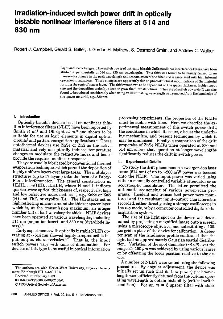
Additional information on the transverse variationin optical constants was obtained by illuminating theirradiated region of the NLIF with a large-area uni-form 514-nm beam at low power and observing a mag-nified image of the effected area. A CCD camera inconjunction with a Hamamatsu image-digitizer/pro-cessor was used to record and analyze the transmissionprofiles. By varying the angle of the NLIF relative tothe probe beam, the induced changes in the maximumtransmission and peak wavelength could be deter-mined as a function of position in the irradiated region.Figure 2 shows, as an example, a pseudo-3D plot of thespatial variation of 514-nm transmission over an areathat was irradiated for -15 min with 30-50 mW ofoptical power focused into a 45-gtm diam spot. Toobtain this plot, the filter was angle-tuned for maxi-mum transmission at the spot center. Similar plotstaken at different angles of incidence provided a fullset of data from which peak wavelength shifts andtransmission changes can be calculated for any chosenposition within the irradiated area.
10 February 1990 / Vol. 29, No. 5 / APPLIED OPTICS 639
1, :, 11 11�

50
o- 70
C-)
20
30
60
Fig. 2. Spatial variation of transmission over the irradiated area fora detuning corresponding to maximum transmission for the center ofthe damaged region. NLIF construction as in Fig. 1. Irradiation
time of -15 min., 30-50 mW into a spot diameter of 45 ,um.
Another aspect of these transverse spatial effects isthe dependence of this predamage phenomenon uponlaser spot size. Figure 3 shows the time for whichbistability was retained for a range of spot sizes. It isclear from these results that the switch-power drift ismuch more rapid with the smaller spot sizes. Thus, asthe spot diameter was reduced from 125 to 25,um, thetime for the bistable region to disappear reduced from-40 to <10 min, for a 13-layer, m = 4, ZnSe NLIF.
To study the influence of the substrate on the driftphenomena, a comparison of the switch drift rate forfilters deposited on glass and sapphire substrates wasmade. This showed that the filters which were grownon glass maintained bistable characteristics for 8 timeslonger than those on sapphire substrates. This alsocorresponded to the ratio of switch powers of the twodevices.
Finally, a further set of experiments was carried outin which the thickness of the central layer was variedbetween 0.2 m (m = 2) and 0.8 ,m (m = 8). Thevariations of switch power observed are summarized inFig. 4. It can be seen that increasing the spacer thick-ness dramatically reduces the rate of drift-in theseexperiments, by >10 times.
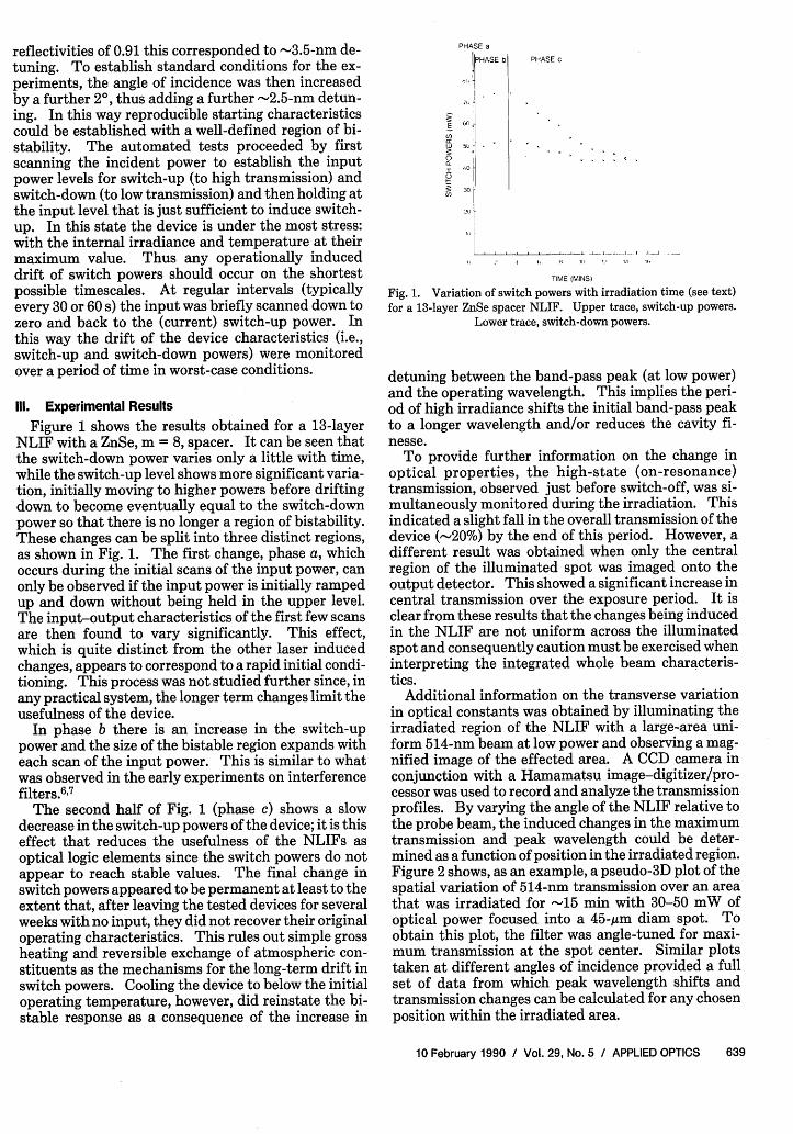
IV. Analysis of ResultsThe transmission values recorded over the damaged
area for different angles of incident (e.g., see Fig. 2),provide sufficient information for the deduction of thetransmission spectra at any position of the illuminatedarea. For example, Fig. 5 compares the central regionspectrum to that of an adjacent nonirradiated area. Inmodeling the properties of these points it was assumedthat any changes in the optical constants of the materi-al were dominantly irradiance dependent (see Sec. 5).Thus, because the irradiance inside the spacer is fargreater than that in the reflecting stacks, it follows thatthe optical constants of the latter can be assumed notto change significantly on irradiation.
Figure 5 compares the experimental transmissionand theoretically fitted spectra, corresponding to the
F
a
at
0
0
qrMu
Po
orLL
40
30
20
10
0 50 100
SPOT DIAMETER(pm)
Fig. 3. Dependence of irradiation time for loss of bistability uponincident spot diameter. The NLIF had a ZnSe spacer and a con-
struction 3(HL) 4(HH) 3(LH).
3.0
C)
3to1
5 10 15 20
TIME (mins)
Fig. 4. Variation of switch powers with irradiation time, for three13-layer NLIFs with (ZnSe) spacer orders: m = 2 (+), m = 4 (0) and
m = 8 (x). Irradiation spot diameter 60 im.
central spot region after irradiation, with spectra de-duced for the nonilluminated area. It can be seen thatthe peak wavelength has shifted by 1.8 nm and themaximum transmission increased from 26 to 34%as a result of the irradiation. The construction of thisfilter was [3(HL)] [8H'H'] [3(LH)], where H and H' arequarter-wave optical thicknesses of ZnS and ZnSe,respectively. The laser beam was incident from thesubstrate side. The optical constants used for model-ing the initial transmission spectrum of the filter werenH = 2.7, nH = 2.5 and nL = 1.5 with an absorptioncoefficient (a) of 1020 cm-' for the spacer layer. Sincethe effect of the stacks is assumed to be constant, only achange in the refractive index of the spacer could pro-duce the resonance peak shift. Similarly, only a de-crease in the absorption coefficient could increase thetransmission and finesse of the damaged spot. In theexample shown in Fig. 5, the refractive index was foundto increase by 0.01 (<1%) (after irradiation) while theabsorption value decreased to 760 cm-1.
640 APPLIED OPTICS / Vol. 29, No. 5 / 10 February 1990
4uu
175 - +
150 + $+ o
125.-,
100 00 0 o00o0o
75
50 . . . . . . . .
25
I
40
e
0
3Ico
as;
0 I I I I I , I
514 516 518 520 522 524
WAVELENGTH (nm)
Fig. 5. Linear transmission pass-band spectrum of (a) an undam-aged region of a filter, and (b) the center of an irradiated (damaged)region. See text for NLIF construction. The curves correspond tocalculated spectra, assuming spacer indices (a) 2.7 and (b) 2.71, and
spacer absorption coefficients (a) 1020 cm-' and (b) 760 cm-'.
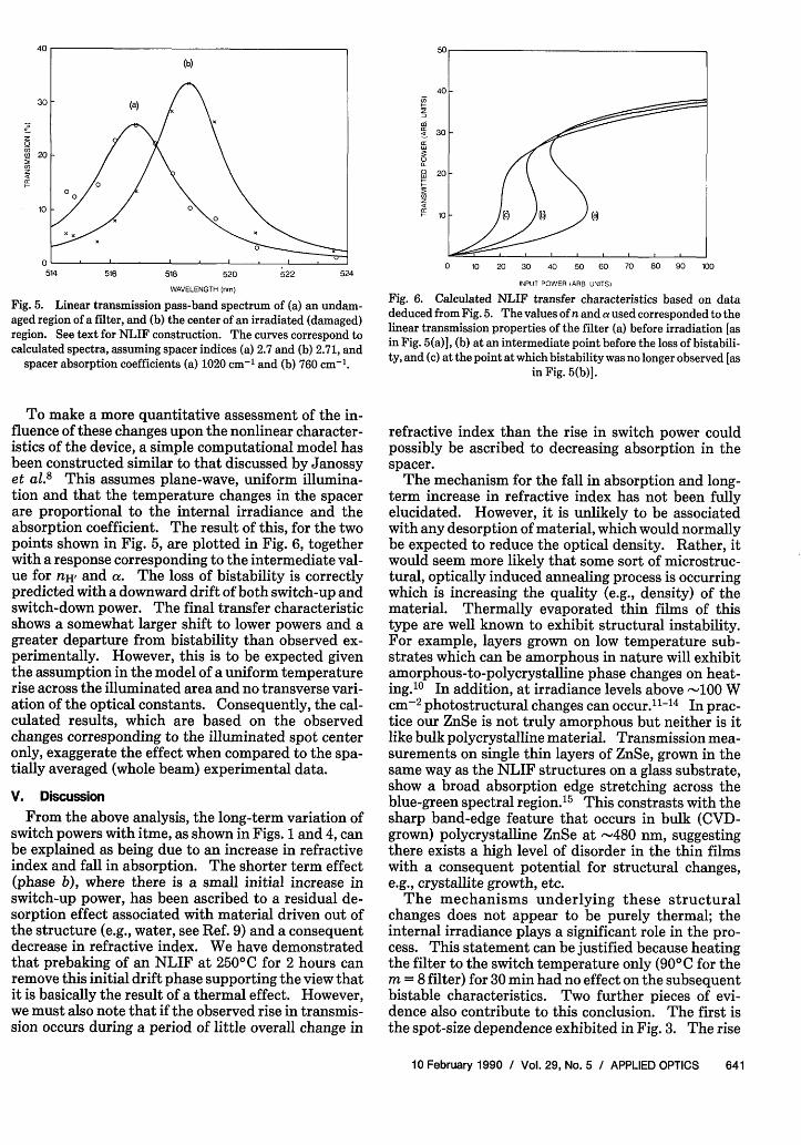
To make a more quantitative assessment of the in-fluence of these changes upon the nonlinear character-istics of the device, a simple computational model hasbeen constructed similar to that discussed by Janossyet al.
8 This assumes plane-wave, uniform illumina-tion and that the temperature changes in the spacerare proportional to the internal irradiance and theabsorption coefficient. The result of this, for the twopoints shown in Fig. 5, are plotted in Fig. 6, togetherwith a response corresponding to the intermediate val-ue for nH' and a. The loss of bistability is correctlypredicted with a downward drift of both switch-up andswitch-down power. The final transfer characteristicshows a somewhat larger shift to lower powers and agreater departure from bistability than observed ex-perimentally. However, this is to be expected giventhe assumption in the model of a uniform temperaturerise across the illuminated area and no transverse vari-ation of the optical constants. Consequently, the cal-culated results, which are based on the observedchanges corresponding to the illuminated spot centeronly, exaggerate the effect when compared to the spa-tially averaged (whole beam) experimental data.
V. DiscussionFrom the above analysis, the long-term variation of
switch powers with itme, as shown in Figs. 1 and 4, canbe explained as being due to an increase in refractiveindex and fall in absorption. The shorter term effect(phase b), where there is a small initial increase inswitch-up power, has been ascribed to a residual de-sorption effect associated with material driven out ofthe structure (e.g., water, see Ref. 9) and a consequentdecrease in refractive index. We have demonstratedthat prebaking of an NLIF at 2500C for 2 hours canremove this initial drift phase supporting the view thatit is basically the result of a thermal effect. However,we must also note that if the observed rise in transmis-sion occurs during a period of little overall change in
at
30-
0
20-
10 P E
0 10 20 30 40 50 60 70 80 90 100
INPUT POWER ARB UNITS)
Fig. 6. Calculated NLIF transfer characteristics based on datadeduced from Fig. 5. The values of n and a used corresponded to thelinear transmission properties of the filter (a) before irradiation [asin Fig. 5(a)], (b) at an intermediate point before the loss of bistabili-ty, and (c) at the point at which bistability was no longer observed [as
in Fig. 5(b)].
refractive index than the rise in switch power couldpossibly be ascribed to decreasing absorption in thespacer.
The mechanism for the fall in absorption and long-term increase in refractive index has not been fullyelucidated. However, it is unlikely to be associatedwith any desorption of material, which would normallybe expected to reduce the optical density. Rather, itwould seem more likely that some sort of microstruc-tural, optically induced annealing process is occurringwhich is increasing the quality (e.g., density) of thematerial. Thermally evaporated thin films of thistype are well known to exhibit structural instability.For example, layers grown on low temperature sub-strates which can be amorphous in nature will exhibitamorphous-to-polycrystalline phase changes on heat-ing.10 In addition, at irradiance levels above -100 Wcm-2 photostructural changes can occur.11-'4 In prac-tice our ZnSe is not truly amorphous but neither is itlike bulk polycrystalline material. Transmission mea-surements on single thin layers of ZnSe, grown in thesame way as the NLIF structures on a glass substrate,show a broad absorption edge stretching across theblue-green spectral region.15 This constrasts with thesharp band-edge feature that occurs in bulk (CVD-grown) polycrystalline ZnSe at -480 nm, suggestingthere exists a high level of disorder in the thin filmswith a consequent potential for structural changes,e.g., crystallite growth, etc.
The mechanisms underlying these structuralchanges does not appear to be purely thermal; theinternal irradiance plays a significant role in the pro-cess. This statement can be justified because heatingthe filter to the switch temperature only (900C for them = 8 filter) for 30 min had no effect on the subsequentbistable characteristics. Two further pieces of evi-dence also contribute to this conclusion. The first isthe spot-size dependence exhibited in Fig. 3. The rise
10 February 1990 / Vol. 29, No. 5 / APPLIED OPTICS 641

in temperature on switching is roughly constant for aparticular NLIF and initial detuning, independent ofspot size. Thus the increase in drift rate with smallspot sizes cannot be ascribed to higher temperatures.The switch irradiance (Is) however, does vary with spotsize. From Janossy et al.,8 it is found thatIS -P,/,rrO 21/ro, where P, is the switch power and r is the spotdiameter. Thus in going from a 125 to a 25-/im spotdiameter the switch irradiance increases by -5 times.(N.B. The switch power falls by a similar factor.8) Theresults in Fig. 3 indicate a similar change in the rate ofswitch power drift.
The second piece of evidence implicating the irradi-ance level as a crucial parameter was obtained fromstudies of the influence of substrate properties. Thetemperature rise required for switching is independentof substrate thermal conductivity K, while the switchpower is proportional to K (in the simplest model).8
Thus higher switching irradiance levels are expectedfor an NLIF deposited on a crystalline heat sink thanfor one on a glass substrate. (N.B. Switch times willalso be proportionally shorter). This was confirmedexperimentally with the filters deposited on the glassand sapphire substrates which had switch powers of9.5 and 80 mW, respectively, for a 10-,gm diam incidentspot size. This 8-fold increase in switch power, andhence internal irradiance, caused a corresponding in-crease in the rate of switch-power drift.
Further contributory evidence comes from the drift-rate dependence upon spacer thickness (m half-wave-lengths), shown in Fig. 4, which indicates much slowerdrift for higher m values. Although the thicker spacerlayers may be structurally more stable (e.g., due togreater crystalline sizes), there should also be a strongdependence of switch power, P8, upon the spacer thick-ness, D. In the circumstances of these experimentswhere the NLIF finesse is relatively high (>5) anddetermined dominantly by the stack reflectivitiesrather than spacer absorption, P8 c D-2 . Assuming aconstant spot size, the switch irradiances increase by afactor of -10 in going from an m = 8 to m = 2 spacer(allowing for the small change in finesse). Thus onceagain there is a strong correlation between drift rateand switch irradiance. However, in these experimentsthe temperature is also changing, as AT, a D-1.8 Con-sequently, the possibility that, in this case, thermalannealing may also be a contributory factor cannot beruled out.
As noted earlier, photostructural effects are seen inamorphous semiconductor films and it would appearthat similar optically induced structural changes areoccurring in these NLIF layers. Incident irradiancelevels at switch-up are typically in the 0.5-10-kW cm-2range. Assuming stack reflectivities of -0.92 and aD-0.02-0.08, then internal irradiances range from 3 kWto -150 kW cm- 2. These are clearly of sufficientmagnitude for photostructural changes to be occurringin the spacer material."
It is concluded that the irreversible changes inducedin the NLIFs occurred in a predamage irradiance re-gime in which photostructural and possibly thermal
12
70$
0
0
5
5
0 -
I
0
-
60 120 180 240 3uu
TIME ON-RESONANCE (mIs.)
Fig. 7. Variation of switch-up powers (upper trace) and switch-down powers (lower trace) for an NLIF with the construction4(H'L)(8H'H')(4LH')Al operated at 830 nm. The incident spot
diameter was -11 jam.
effects played significant roles. The irradiance de-pendent mechanism remains to be determined butcould be associated with free carrier excitation as sug-gested in Ref. 13.
VI. Techniques for Reducing Drift EffectsTo test whether the drift effects are wavelength
dependent, a filter was made with a peak wavelength of830 nm (i.e., corresponding to the output of GaAs laserdiodes). The filter was designed with a BEAT (bi-stable etalon with absorbed transmission)' 6 type con-struction so as to allow milliwatt operation despite thesmall absorption of ZnSe at this wavelength. Thefilter design was glass/4(H'L)/8(H'H')/4(LH')/Al.The role of the aluminum (Al) layer was to absorb thelight transmitted through the etalon, thus providingthe thermal feedback required for bistable switching(at 514 nm this is provided by the absorption in thespacer). For an 11-,um laser spot the critical switchpower of the filter was measured to be typically 3 mW.5This filter, tested in a manner similar to that describedin Sec. II, showed much less switch power drift than the514-nm devices. Figure 7 shows a typical drift resultfor a filter operated at this wavelength. During thefirst 3 h of operation there is some slow change in theswitch-power levels after which they settle to constantvalues. This shows a >30-fold improvement in stabil-ity, despite the internal irradiance being -10 timesgreater and the laser spot size being approximately afactor of 6 smaller.
A similar wavelength dependent peak shift was re-ported by Title' 4 for ZnS interference filters illuminat-ed with low intensity light over a period of severalmonths. Yokoyama has also observed this type ofwavelength dependence 3 for laser-enhanced growthof crystalline ZnSe. It would appear that the furtherthe filter is operated from the material band-edge, themore stable the characteristics will be.
It is also apparent, from the analysis in the previoussection, that the rate of switch-power drift can bedecreased by minimizing the operating internal irradi-
642 APPLIED OPTICS / Vol. 29, No. 5 / 10 February 1990
2
akj
ance. This can be achieved by using larger illumina-tion spot sizes, but at the expense of higher switchpowers and longer response times.8 Lower conductiv-ity substrates would reduce switch irradiance levelsbut again would increase the response time. Morepreferable is the alternative of employing thicker spac-ers (see Fig. 4), which besides reducing the internalirradiance and temperature changes can also reducethe switch power17 without significantly changing theresponse time.
It would clearly also be preferable to use betterquality thin-film material to make up the structure.We are currently investigating the exploitation of mo-lecular beam deposition (MBD) techniques in this con-text. This entails the use of UHV deposition equip-ment originally developed for epitaxial growth of highquality crystalline semiconductor films, as discussedmore fully by Lewis et al.1
8 In addition to providingbetter quality material, the MBD technique permitsthe growth of mechanically stable thick layers (e.g.,.10 gim). This has allowed a wider range of spacer
thicknesses to be obtained for NLIF optimization ex-periments.19 For comparison purposes, an NLIF (op-erated at 514 nm) with a MBD-grown spacer layer wastested for switch-power drift with the standard meth-od described in Sec. II. This particular device wasgrown on a glass substrate with conventional thermallyevaporated reflecting stacks [each 2(HL)] depositedbefore and after the growth of the 2.46-Am thick MBDZnSe spacer. For a 30-,um diam spot, only slow driftwas observed over a 75-min period, due to a variety ofexternal influences (e.g., room temperature changes,mechanical alignment, etc.), and a bistable responsewas maintained throughout-a considerable improve-ment over the earlier 514-nm NLIF designs.
In conclusion, it has been shown that significantswitch-power drift can occur in nSe NLIF devicesand that this can be associated with high internalirradiance levels and the wavelength of operation. Al-though the precise mechanism is not understood thepredamage structural changes cause an increase inrefractive index and a decrease in absorption withinthe spacer layer. This effect can be minimized byusing thicker spacer layers and longer wavelength ofoperation and should be entirely eliminated if theNLIF could be fabricated using structurally stablematerial. To this end, molecular beam deposition(MBD) is currently being investigated as a techniquefor providing such higher quality thin-film material foruse at a variety of wavelengths, particularly those wellremoved from the band-edge of ZnSe (e.g., at 830 nm).
The assistance of OCLI Optical Coatings, Ltd., inpreparing the thermally evaporated multilayer struc-ture is appreciated. The MBD-spacer filter was grownby Keith Lewis at the Royal Signals & Radar Estab-lishment, Malvern, and the assistance of both him andhis colleagues is gratefully acknowledged. This workwas financially supported by the U.K. Science & Engi-neering Research Council (GR/C/59635), the U.K.Ministry of Defence (2195/014/DCVD), and the Com-
mission of the European Communities through theEuropean Joint Optical Bistability Project (EJOB).
References1. S. D. Smith, J. G. H. Mathew, M. R. Taghizadeh, A. C. Walker,
B. S. Wherrett, and A. Hendry, "Room Temperature, VisibleWavelength Optical Bistability in ZnSe Interference Filters,"Opt. Commun. 51, 357-362 (1984).
2. G. R. Olbright, N. Peyghambarian, H. M. Gibbs, H. A. MacLeod,and F. Van Milligen, "Microsecond Room-Temperature OpticalBistability and Cross-Talk Studies in ZnS and ZnSe Interfer-ence Filters with Visible Light and Milliwatt Powers," Appl.Phys. Lett. 45, 1031-1033 (1984).
3. S. D. Smith, A. C. Walker, F. A. P. Tooley and B. S. Wherrett,"The Demonstration of Restoring Digital Optical Logic," Na-ture London 325, 27-31 (1987).
4. M. T. Tsao et al., "Symbolic Substitution Using ZnS Interfer-ence Filters," Opt. Eng. 26, 41-44 (1986).
5. G. S. Buller, C. R. Paton, S. D. Smith, and A. C. Walker, "Opti-cally Bistable Nonlinear Interference Filters for Use with Near-Infrared Laser Diodes," Opt. Commun. 70, 522-528 (1989).
6. F. V. Karpushko and G. V. Sinitsyn, "An Optical Logic Elementfor Integrated Optics in a Nonlinear Semiconductor Interfero-meter," J. Appl. Spectrosc. USSR 29, 1323-1326 (1978).
7. H. M. Gibbs, Optical Bistability: Controlling Light with Light(Academic, New York, 1955) p. 122.
8. I. Janossy, M. R. Taghizadeh, J. G. H. Mathew, and S. D. Smith,"Thermally Induced Optical Bistability in Thin-Film Devices,"IEEE J. Quantum Electron. QE-21, 1447-1452 (1985).
9. P. Roche, L. Bertrand, and E. Pelletier, "Influence of Tempera-ture on the Optical Properties of Narrow-Band InterferenceFilters," Opt. Acta 23, 433-444 (1976).
10. J. F. Gibbons, Ed., Semiconductors and Semimetals, Vol. 17(Academic, New York, 1984), p. 2.
11. S. Sugai, "Two-Directional Photoinduced Crystallisation inGaSe2 and SiSe2 Glasses," Phys. Rev. Lett. 57, 456-459 (1986).
12. J. Hajto and I. Janossy, "Optical Bistability Observed in Amor-phous Semiconductor Films," Philos. Mag. B 47, 347-366(1983).
13. M. Yokoyama, "Photoinduced Surface Morphology Improve-ments and Preferential Orientation Enhancement in Film De-position of Evaporated ZnS," Appl. Phys. Lett. 49, 1354-1356(1986).
14. A. M. Title, "Drift in Interference Filters. 2: Radiation Ef-fects," Appl. Opt. 13, 2680-2684 (1974).
15. A. C. Walker and F. A. P. Tooley, "Studies of Electronic Nonlin-earities in InSb and Thermal Nonlinearities in InSb and Zn," inOptical Bistability Towards Optical Computing, P. Mandel, S.D. Smith, and B. S. Wherrett, Eds. (North-Holland, Amster-dam, 1987), pp. 49-58.
16. A. C. Walker, "Reflection Bistable Etalons with AbsorbedTransmission," Opt. Commun. 59, 145-150 (1986).
17. B. S. Wherrett, D. Hutchings, and D. Russell, "Optically Bi-stable Interference Filters: Optimization Considerations," J.Opt. Soc. Am. B 3, 351-362 (1986).
18. K. L. Lewis and J. A. Savage, Proceedings of the Symposium onLaser Induced Damage in Optical Materials, National Bureauof Standards, Nat. Bur. Stand. (U.S.) Spec. Publ. 688 (1985), p.277.
19. Y. T. Chow et al., "Continuous-Wave Laser-Pumped OpticalBistability in Thermally Deposited and Molecular-Beam-Grown ZnSe Interference Filters," J. Opt. Soc. Am. B 3, 1535-1539 (1986).
10 February 1990 / Vol. 29, No. 5 / APPLIED OPTICS 643