IP Solutions for a Data-Centric World
7
WHITE PAPER IP Solutions for a Data-Centric World By Arif Khan, Cadence We’re in an era of sizeable growth in data and compute demand, along with increasing global data traffic. As a result, high-performance computing, data communications, networking, and storage systems are taking center stage in many application areas, driven by newer applications such as analytics, artificial intelligence (AI), genomics, and simulation-intensive workloads. Power efficiency, high performance and uptime, and small form factor (also referred to as power, performance, and area (PPA) are some of the key requirements for such systems, and these requirements impact their underlying electronic components and intellectual property (IP) building blocks. That’s why it’s essential for you to ensure that every level of your design meets these requirements and that each component operates as intended on its own and within the context of the entire communications infrastructure system. In this paper, we will examine how Cadence’s pre-verified, standards-based design IP can help in this regard, giving you the ability to deliver on your quality and time-to-market goals. Contents Introduction.................................................................2 Challenges of Designing for the Zettabyte Era ..............................................................2 Advantages of Designing with Pre-Verified IP.............................................................3 Integration-Focused IP and IP Subsystems......5 Optimizing Electronic System Design .................6 Summary ...................................................................... 7
Transcript of IP Solutions for a Data-Centric World
WHITE PAPER
IP Solutions for a Data-Centric WorldBy Arif Khan, Cadence
We’re in an era of sizeable growth in data and compute demand, along with increasing
global data traffic. As a result, high-performance computing, data communications,
networking, and storage systems are taking center stage in many application areas,
driven by newer applications such as analytics, artificial intelligence (AI), genomics, and
simulation-intensive workloads. Power efficiency, high performance and uptime, and
small form factor (also referred to as power, performance, and area (PPA) are some of
the key requirements for such systems, and these requirements impact their underlying
electronic components and intellectual property (IP) building blocks. That’s why it’s
essential for you to ensure that every level of your design meets these requirements and
that each component operates as intended on its own and within the context of the
entire communications infrastructure system. In this paper, we will examine how
Cadence’s pre-verified, standards-based design IP can help in this regard, giving you the
ability to deliver on your quality and time-to-market goals.
Contents
Introduction .................................................................2
Challenges of Designing for the Zettabyte Era ..............................................................2
Advantages of Designing with Pre-Verified IP .............................................................3
Integration-Focused IP and IP Subsystems ......5
Optimizing Electronic System Design .................6
Summary ......................................................................7
IP Solutions for a Data-Centric World
2www.cadence.com
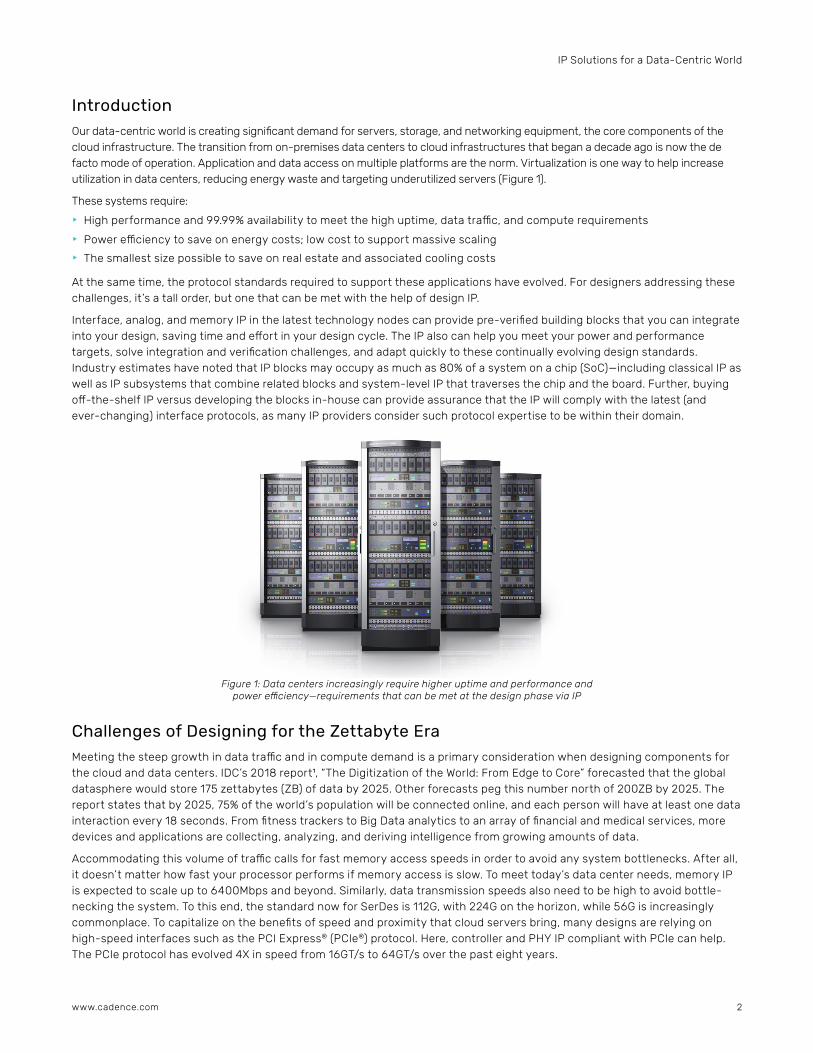
IntroductionOur data-centric world is creating significant demand for servers, storage, and networking equipment, the core components of the cloud infrastructure. The transition from on-premises data centers to cloud infrastructures that began a decade ago is now the de facto mode of operation. Application and data access on multiple platforms are the norm. Virtualization is one way to help increase utilization in data centers, reducing energy waste and targeting underutilized servers (Figure 1).
These systems require:
f High performance and 99.99% availability to meet the high uptime, data traffic, and compute requirements
f Power efficiency to save on energy costs; low cost to support massive scaling
f The smallest size possible to save on real estate and associated cooling costs
At the same time, the protocol standards required to support these applications have evolved. For designers addressing these challenges, it’s a tall order, but one that can be met with the help of design IP.
Interface, analog, and memory IP in the latest technology nodes can provide pre-verified building blocks that you can integrate into your design, saving time and effort in your design cycle. The IP also can help you meet your power and performance targets, solve integration and verification challenges, and adapt quickly to these continually evolving design standards. Industry estimates have noted that IP blocks may occupy as much as 80% of a system on a chip (SoC)—including classical IP as well as IP subsystems that combine related blocks and system-level IP that traverses the chip and the board. Further, buying off-the-shelf IP versus developing the blocks in-house can provide assurance that the IP will comply with the latest (and ever-changing) interface protocols, as many IP providers consider such protocol expertise to be within their domain.
Challenges of Designing for the Zettabyte EraMeeting the steep growth in data traffic and in compute demand is a primary consideration when designing components for the cloud and data centers. IDC’s 2018 report1, “The Digitization of the World: From Edge to Core” forecasted that the global datasphere would store 175 zettabytes (ZB) of data by 2025. Other forecasts peg this number north of 200ZB by 2025. The report states that by 2025, 75% of the world’s population will be connected online, and each person will have at least one data interaction every 18 seconds. From fitness trackers to Big Data analytics to an array of financial and medical services, more devices and applications are collecting, analyzing, and deriving intelligence from growing amounts of data.
Accommodating this volume of traffic calls for fast memory access speeds in order to avoid any system bottlenecks. After all, it doesn’t matter how fast your processor performs if memory access is slow. To meet today’s data center needs, memory IP is expected to scale up to 6400Mbps and beyond. Similarly, data transmission speeds also need to be high to avoid bottle-necking the system. To this end, the standard now for SerDes is 112G, with 224G on the horizon, while 56G is increasingly commonplace. To capitalize on the benefits of speed and proximity that cloud servers bring, many designs are relying on high-speed interfaces such as the PCI Express® (PCIe®) protocol. Here, controller and PHY IP compliant with PCIe can help. The PCIe protocol has evolved 4X in speed from 16GT/s to 64GT/s over the past eight years.
Figure 1: Data centers increasingly require higher uptime and performance and power efficiency—requirements that can be met at the design phase via IP
IP Solutions for a Data-Centric World
3www.cadence.com
Power is another key consideration, since data centers not only have high energy consumption, but also generate a lot of heat. U.S. data centers consume from 1.5 to 3% of the country’s energy production. Multiply the power consumption of all of the servers in a typical data center, and you can see that cooling the equipment becomes a considerably complex task. Past research has indicated that active servers use less than 20% of data center energy, while a substantial amount of energy is used to cool the servers and to support power consumption in idle states2. Large cloud providers such as Google focus on data center power usage effectiveness (PUE) to ensure that data centers are designed to use energy in the most efficient manner.3
Designing networking and other data center components is not getting any easier for other reasons as well. Meeting the power and performance needs of these designs pushes the technology envelope toward advanced geometries. From TSMC’s Q3 2020 earnings report4, over one-third of the quarter’s revenue was driven by AI and over half of it in advanced finFET technologies. At smaller geometries, you gain the advantages of a better power/performance mix, but you also face increased parasitics, challenging layout due to double and even triple patterning, and expanded design rule checks (DRCs). Larger designs are hitting the limits of Moore’s law and solutions relying on advanced interconnect such as high-bandwidth interface (HBI) and die-to-die interface are required to implement these solutions.
With time-to-market pressures always looming, your schedules are greatly constrained. In some cases, you may not be able to wait until a standard has been finalized if you’re aiming to capture a particular market opportunity.
Advantages of Designing with Pre-Verified IPPre-verified design and verification IP can help ease your design process, accelerate your time to market, and help you meet key considerations when designing SoCs for enterprise-level communications and storage systems:
f Compliance with industry standards
f Performance and power targets
f Customization requirements
f Reduced integration and verification effort
f Design risk mitigation
f High robustness for signal noise
Compliance with industry standards
IP really excels when it comes to supporting industry standards and helping you overcome any challenges or barriers related to knowledge gaps on a given standard. IP vendors gain a deep understanding of specifications, developing their IP according to the requirements of each standard. As a result, you don’t have to worry about keeping up to date with specification changes and can be assured that your design will, in turn, meet the PPA, bandwidth, and other relevant specifications. You can then focus more of your time on design priorities that provide differentiation for your SoC, rather than poring through hundreds of pages of specification guidelines for each protocol that your design needs to support.
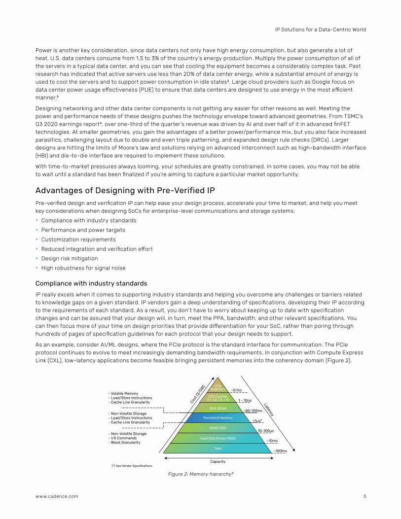
As an example, consider AI/ML designs, where the PCIe protocol is the standard interface for communication. The PCIe protocol continues to evolve to meet increasingly demanding bandwidth requirements. In conjunction with Compute Express Link (CXL), low-latency applications become feasible bringing persistent memories into the coherency domain (Figure 2).
CPU Registers ~0.1ns
1 - 10ns
~80-100ns
10-100us
~10ms
~100ms
<1us*
CPU Caches (L1, L2, L3, L4)
DDR DRAM
Persistent Memory
NAND SSD
Hard Disk Drives (HDD)
Tape
Capacity(*) See Vendor Specifications
- Non-Volatile Storage- I/O Commands- Block Granularity
- Non-Volatile Storage- Load/Store Instructions- Cache Line Granularity
- Volatile Memory- Load/Store Instructions- Cache Line Granularity
Figure 2: Memory hierarchy5

IP Solutions for a Data-Centric World
4www.cadence.com
PCIe and CXL 2.0 Controller and PHY IP products can help you meet changing PPA requirements. Hard IP (IP delivered as GDSII) can help you handle extreme operating temperature ranges over an extended period of time, as well as manage the effects of electromigration/IR drop (EM-IR)—important considerations in a networking or data center environment. Hard IP undergoes thorough testing under a variety of conditions, such as extreme operating temperatures, and is built to be durable beyond some single point in order to accommodate designers with different operating condition requirements. In fact, while standards generally address a common need, IP providers often go beyond the specifications outlined in the standards for factors such as temperate range, signal strength, noise tolerance, and voltage differences between SoCs to provide increased robustness in real-world environments.
Power and performance targets
The performance and power specifications discussed in the previous section are in the realm of the market’s available IP offerings. For example, Cadence® Denali® DDR controller and PHY IP support the latest protocols such as GDDR6 and DDR5/LPDDR5 and high-bandwidth memory (HBM). Cadence also offers a 32Gbps Multi-Protocol and Multi-Link PHY IP for PCIe 5.0 that operates at speeds from 1.25Gbps to 32Gbps and meets the most stringent data center and networking requirements: 10-year lifetime and 110°C for electromigration, all while operating at the lowest active power. These IP products are available in advanced finFET nodes needed to meet the performance targets for data-centric, high-performance computing (HPC)/AI applications.
PCIe 5.0, in particular, addresses the need for high performance and low latency to support east-west traffic, providing much needed capabilities including 32Gbps transfer speed (scalable to 512Gbps (x16)), multi-CPU data analytics, and broad deployment. Figure 3 compares old data center demands with new, where the emphasis is on east-west linear scalability. Cadence, in particular, has optimized its PCIe controller and PHY to provide significant power reductions at the highest active speeds while maintaining leadership in the lower power modes.
Considering the cost and effort of chip design, you may want to future-proof your designs by adapting one design for multiple target systems. For this approach, you would need to be able to adapt quickly to different standards. IP with support for multiple protocols can give you the flexibility to modify your design to accommodate standards across a range of application areas. Furthermore, the ability to multiplex a single port for different protocols also allows you to use one chip for different applications. For example, you might adapt your chip to an application that calls for PCIe x16 lane support and utilize the same chip for another application requiring PCIe x8 lane support and eight lanes for another communications protocol.
Figure 3: Requirements for meeting today’s data center demands
WAN Core Router
Fibre Channel Gateway
Fibre Channel Storage
OLD NEW
WAN Core Router
Difficult East-West ScalabilityHigh East-West LatencyComplex and Costly Switches
East-West Linear ScalabilityConsistent East-West LatencySimpler Cost-Effective Switches

IP Solutions for a Data-Centric World
5www.cadence.com
Customization requirements
IP designed with a configurable architecture, along with software and prototyping solutions, can help you meet your customi-zation requirements. Select an IP vendor who can provide specific features and performance levels targeted to your unique SoC design. This way, you can integrate the IP into your design, rather than having to build your design around the IP.
Reduced integration and verification effort
Integrating IP into your design can be a challenge, but much less so if you are using IP and IP subsystems designed from the ground up with an integration focus. Controller, PHY, and firmware solutions that are fully integrated at the interface and subsystem levels can reduce your design risks as well as your integration effort. By the same token, being able to use fully verified IP from a vendor saves you the step of doing the groundwork to ensure that the IP will work with your design.
Design risk mitigation
The breadth of verification in the IP is another important consideration. Not all IP vendors are the same in this regard. IP vendors who are focused on early development of IP, collaborating closely with end customers as they build out their SoCs, have an advantage. These vendors are privy to insights about design challenges as their customers encounter them, so they can adjust and update their IP accordingly. They build into their design process all of their lessons learned and continue to enhance future iterations of IP. Also, the more customers an IP vendor works with, the more access the vendor has to platforms on which to test their IP, ultimately helping you mitigate your design risks. Not every vendor has the ability to continually gather data about interoperability and also ensure verification of their IP across multiple platforms.
Integration-Focused IP and IP SubsystemsIn Cadence’s broad portfolio of fully verified design IP, you can find cores that are ideally suited to SoCs for communications infrastructure applications such as servers, storage systems, and networking equipment. Cadence focuses on early development of IP, building its products from the ground up while working closely with multiple customers who integrate the IP into their designs as they are building them. As customers test and verify their designs while progressing toward tapeout, our IP developers test the IP along with way, providing the benefits of distributed verification. With access to so much silicon data early on, our IP developers can quickly understand advanced processes and their limitations, as well as challenges, and incorporate what they’re learning into each generation of IP.
As an early driver of standards compliance, Cadence often plays a role in standards definition. Our technical experts are part of the working groups for various standards organizations. As another example, we were the first IP vendor to bring PCIe 3.0 controllers to market and today, our controller and PHY IP for PCIe supports the latest specification (5.0). Because we certify our IP in silicon, you can be assured that your design can pass the same certification.
Cadence develops integration-focused IP and IP subsystems that have demonstrated the ability to reduce risk and to accelerate SoC development. Strong relationships with foundries mean early access to their processes and, as a result, the ability to proceed with early development, validation, and certification.
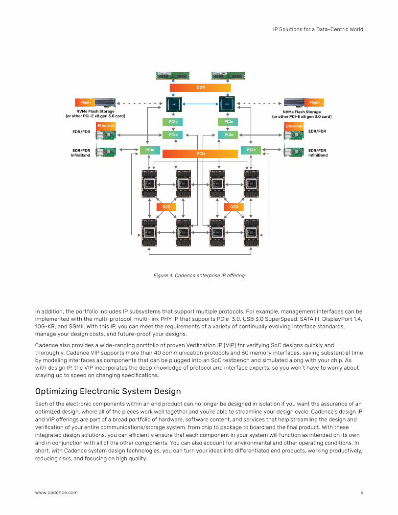
For enterprise-level data communications and storage systems, Cadence offers a variety of relevant design IP to meet performance, power efficiency, and other requirements (Figure 4), including:
f 32Gbps SerDes PHY IP for PCIe 5.0 for inter-device communication between chips, between boards, and between systems; high-performance data communication; high-performance storage access; and high-performance data center communication. In conjunction with CXL, it offers a low-latency solution for coherent systems.
f GDDR6 and DDR/LPDDR5/4 controller and PHY IP providing low-latency data access and enhanced memory utilization, such as for Big Data local computation support. Features such as error correction code (ECC), parity, and memory built-in self-test (MBIST) enhance data reliability by minimizing undetectable data corruption in high-density computing environments.
f Interconnect solutions such as Cadence UltraLink™ D2D PHY IP (die-to-die) solutions and HBI for chiplet implementations.
f NAND Flash IP, providing fast Boot ROM code storage.
f High-speed SerDes offerings for 56G/112G supporting 40+dB insertion loss with significant power advantages.
IP Solutions for a Data-Centric World
6www.cadence.com
In addition, the portfolio includes IP subsystems that support multiple protocols. For example, management interfaces can be implemented with the multi-protocol, multi-link PHY IP that supports PCIe 3.0, USB 3.0 SuperSpeed, SATA III, DisplayPort 1.4, 10G-KR, and SGMII. With this IP, you can meet the requirements of a variety of continually evolving interface standards, manage your design costs, and future-proof your designs.
Cadence also provides a wide-ranging portfolio of proven Verification IP (VIP) for verifying SoC designs quickly and thoroughly. Cadence VIP supports more than 40 communication protocols and 60 memory interfaces, saving substantial time by modeling interfaces as components that can be plugged into an SoC testbench and simulated along with your chip. As with design IP, the VIP incorporates the deep knowledge of protocol and interface experts, so you won’t have to worry about staying up to speed on changing specifications.
Optimizing Electronic System DesignEach of the electronic components within an end product can no longer be designed in isolation if you want the assurance of an optimized design, where all of the pieces work well together and you’re able to streamline your design cycle. Cadence’s design IP and VIP offerings are part of a broad portfolio of hardware, software content, and services that help streamline the design and verification of your entire communications/storage system, from chip to package to board and the final product. With these integrated design solutions, you can efficiently ensure that each component in your system will function as intended on its own and in conjunction with all of the other components. You can also account for environmental and other operating conditions. In short, with Cadence system design technologies, you can turn your ideas into differentiated end products, working productively, reducing risks, and focusing on high quality.
Server Block DiagramNumberSmasher 4U Tesla 8-GPU Server with NVLink
PCIe
PCIe
PCIe
PCIe
Ethernet
D2DD2D
Flash
Ethernet
Flash
NVMe Flash Storage(or other PCI-E x8 gen 3.0 card)
NVMe Flash Storage(or other PCI-E x8 gen 3.0 card)
EDR/FDR
EDR/FDRInfiniBand
EDR/FDR
EDR/FDRInfiniBand
DDR
PCIe PCIe
PCIe
Figure 4: Cadence enterprise IP offering
IP Solutions for a Data-Centric World
Cadence is a pivotal leader in electronic design and computational expertise, using its Intelligent System Design strategy to turn design concepts into reality. Cadence customers are the world’s most creative and innovative companies, delivering extraordinary electronic products from chips to boards to systems for the most dynamic market applications. www.cadence.com
© 2021 Cadence Design Systems, Inc. All rights reserved worldwide. Cadence, the Cadence logo, and the other Cadence marks found at www.cadence.com/go/trademarks are trademarks or registered trademarks of Cadence Design Systems, Inc. PCI Express and PCIe are registered trademarks or trademarks of PCI-SIG. All other trademarks are the property of their respective owners. 15844 03/21 SA/VY/PDF
SummaryIncreased reliance on servers, storage systems, networking equipment, and other communications infrastructure applications mean that high performance and uptime, low power consumption, and reduced area are more critical than ever for the underlying SoCs. Cadence’s proven, pre-verified design, analog, and memory IP and VIP go a long way in helping you mitigate design risks, lower costs, and meet PPA and time-to-market targets.
References1. David Reinsel, John Gantz, and John Rydning, “The Digitization of the World from Edge to Core”, an IDC White Paper
Sponsored by Seagate, November 2018: https://www.seagate.com/files/www-content/our-story/trends/files/idc-sea-gate-dataage-whitepaper.pdf
2. Arif Khan and Osman Javed, “Software and System Solutions Drive Datacenter Efficiency,” Electronic Design, October 2013: http://electronicdesign.com/power/software-and-system-solutions-drive-datacenter-energy-efficiency
3. “Efficiency”, Google Data Centers:https://www.google.com/about/datacenters/efficiency/
4. “2020 Third-Quarter Earnings Conference” TSMC, October 15, 2020: https://investor.tsmc.com/english/encrypt/files/encrypt_file/qr/phase5_support/3Q20PresentationUpload%28E%29.pdf
5. Persistent Memory Documentation: https://docs.pmem.io/persistent-memory/getting-started-guide/introduction