
IO60-M410 - WinSystems · The IO60-M410 is a data acquisition module for embedded systems with IO60...
27
WinSystems, Inc. | 715 Stadium Drive, Arlington, Texas 76011 | 817-274-7553 | [email protected] | www.winsystems.com IO60-M410 Data Acquisition Module Product Manual
Transcript of IO60-M410 - WinSystems · The IO60-M410 is a data acquisition module for embedded systems with IO60...

IO60-M410Data Acquisition Module
Product Manual
WinSystems, Inc. | 715 Stadium Drive, Arlington, Texas 76011 | 817-274-7553 | [email protected] | www.winsystems.com
IO60-M410
v1.0
Revision History
Copyright and TrademarksCopyright 2015, WinSystems, Inc.
No part of this document may be copied or reproduced in any form or by any means without the prior written consent of WinSystems, Inc. The information in the document is subject to change without notice. The information furnished by WinSystems, Inc. in this publication is believed to be accurate and reliable. However, WinSystems, Inc. makes no warranty, express, statutory, implied or by description, regarding the information set forth herein or regarding the freedom of the described devices from patent infringement. WinSystems, Inc. makes no warranty of merchantability or fitness for any purpose. WinSystems, Inc. assumes no responsibility for any errors that may appear in this document.
Trademark Acknowledgments
WinSystems is a registered trademark of WinSystems, Inc.
Duo-Clasp™ and Pico-Clasp™ are registered trademarks of Molex, Inc.
Analog Devices and RTI are registered trademarks of Analog Devices.
Linear Technology is a registered trademark of Linear Technology, Inc.
Ethernet is a trademark of Xerox Corporation.
Document Version
Last Updated Date Brief Description of Change
v1.0 08/2015 Initial release
www.winsystems.com Page i
IO60-M410
v1.0
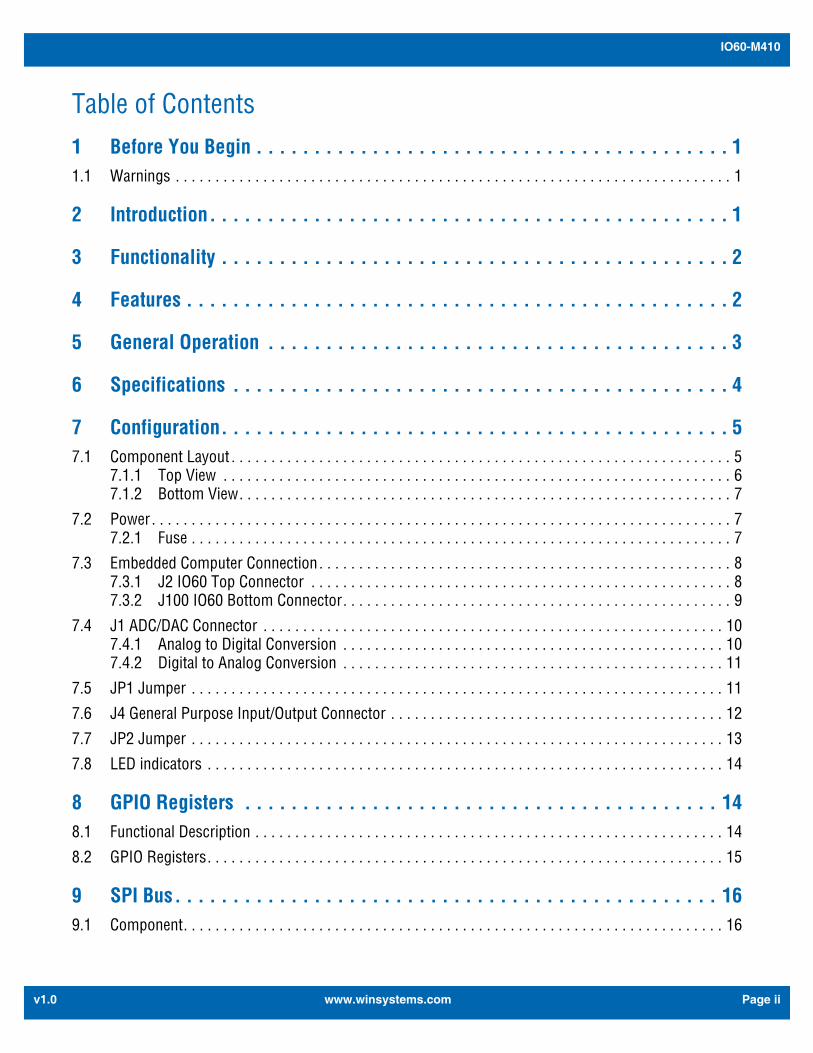
Table of Contents
1 Before You Begin . . . . . . . . . . . . . . . . . . . . . . . . . . . . . . . . . . . . . . . . . 11.1 Warnings . . . . . . . . . . . . . . . . . . . . . . . . . . . . . . . . . . . . . . . . . . . . . . . . . . . . . . . . . . . . . . . . . . . . . . 12 Introduction. . . . . . . . . . . . . . . . . . . . . . . . . . . . . . . . . . . . . . . . . . . . . 1
3 Functionality . . . . . . . . . . . . . . . . . . . . . . . . . . . . . . . . . . . . . . . . . . . . 2
4 Features . . . . . . . . . . . . . . . . . . . . . . . . . . . . . . . . . . . . . . . . . . . . . . . 2
5 General Operation . . . . . . . . . . . . . . . . . . . . . . . . . . . . . . . . . . . . . . . . 3
6 Specifications . . . . . . . . . . . . . . . . . . . . . . . . . . . . . . . . . . . . . . . . . . . 4
7 Configuration. . . . . . . . . . . . . . . . . . . . . . . . . . . . . . . . . . . . . . . . . . . . 57.1 Component Layout . . . . . . . . . . . . . . . . . . . . . . . . . . . . . . . . . . . . . . . . . . . . . . . . . . . . . . . . . . . . . . . 5
7.1.1 Top View . . . . . . . . . . . . . . . . . . . . . . . . . . . . . . . . . . . . . . . . . . . . . . . . . . . . . . . . . . . . . . . . 67.1.2 Bottom View. . . . . . . . . . . . . . . . . . . . . . . . . . . . . . . . . . . . . . . . . . . . . . . . . . . . . . . . . . . . . . 7
7.2 Power. . . . . . . . . . . . . . . . . . . . . . . . . . . . . . . . . . . . . . . . . . . . . . . . . . . . . . . . . . . . . . . . . . . . . . . . . 77.2.1 Fuse . . . . . . . . . . . . . . . . . . . . . . . . . . . . . . . . . . . . . . . . . . . . . . . . . . . . . . . . . . . . . . . . . . . . 7
7.3 Embedded Computer Connection. . . . . . . . . . . . . . . . . . . . . . . . . . . . . . . . . . . . . . . . . . . . . . . . . . . . 87.3.1 J2 IO60 Top Connector . . . . . . . . . . . . . . . . . . . . . . . . . . . . . . . . . . . . . . . . . . . . . . . . . . . . . 87.3.2 J100 IO60 Bottom Connector. . . . . . . . . . . . . . . . . . . . . . . . . . . . . . . . . . . . . . . . . . . . . . . . . 9
7.4 J1 ADC/DAC Connector . . . . . . . . . . . . . . . . . . . . . . . . . . . . . . . . . . . . . . . . . . . . . . . . . . . . . . . . . . 107.4.1 Analog to Digital Conversion . . . . . . . . . . . . . . . . . . . . . . . . . . . . . . . . . . . . . . . . . . . . . . . . 107.4.2 Digital to Analog Conversion . . . . . . . . . . . . . . . . . . . . . . . . . . . . . . . . . . . . . . . . . . . . . . . . 11
7.5 JP1 Jumper . . . . . . . . . . . . . . . . . . . . . . . . . . . . . . . . . . . . . . . . . . . . . . . . . . . . . . . . . . . . . . . . . . . 11
7.6 J4 General Purpose Input/Output Connector . . . . . . . . . . . . . . . . . . . . . . . . . . . . . . . . . . . . . . . . . . 12
7.7 JP2 Jumper . . . . . . . . . . . . . . . . . . . . . . . . . . . . . . . . . . . . . . . . . . . . . . . . . . . . . . . . . . . . . . . . . . . 13
7.8 LED indicators . . . . . . . . . . . . . . . . . . . . . . . . . . . . . . . . . . . . . . . . . . . . . . . . . . . . . . . . . . . . . . . . . 14
8 GPIO Registers . . . . . . . . . . . . . . . . . . . . . . . . . . . . . . . . . . . . . . . . . 148.1 Functional Description . . . . . . . . . . . . . . . . . . . . . . . . . . . . . . . . . . . . . . . . . . . . . . . . . . . . . . . . . . . 14
8.2 GPIO Registers. . . . . . . . . . . . . . . . . . . . . . . . . . . . . . . . . . . . . . . . . . . . . . . . . . . . . . . . . . . . . . . . . 15
9 SPI Bus. . . . . . . . . . . . . . . . . . . . . . . . . . . . . . . . . . . . . . . . . . . . . . . 169.1 Component. . . . . . . . . . . . . . . . . . . . . . . . . . . . . . . . . . . . . . . . . . . . . . . . . . . . . . . . . . . . . . . . . . . . 16
www.winsystems.com Page ii

IO60-M410
v1.0
9.2 Features . . . . . . . . . . . . . . . . . . . . . . . . . . . . . . . . . . . . . . . . . . . . . . . . . . . . . . . . . . . . . . . . . . . . . . 16
9.3 SPI Commands . . . . . . . . . . . . . . . . . . . . . . . . . . . . . . . . . . . . . . . . . . . . . . . . . . . . . . . . . . . . . . . . 17
10 Other Registers . . . . . . . . . . . . . . . . . . . . . . . . . . . . . . . . . . . . . . . . . 18
Appendix A. Best Practices . . . . . . . . . . . . . . . . . . . . . . . . . . . . . . . . . . . . 19
Appendix B. Mechanical Drawing . . . . . . . . . . . . . . . . . . . . . . . . . . . . . . . 22
Appendix C. Warranty Information . . . . . . . . . . . . . . . . . . . . . . . . . . . . . . . 23
www.winsystems.com Page iii
IO60-M410/Before You Begin
v1.0
1. Before You BeginReview the warnings (in this section) and the best practice recommendations (see “Best Practices” on page 19) when using and handling the WinSystems IO60-M410. Following these recommendations provides an optimal user experience and prevents damage. Read through this document and become familiar with the IO60-M410 before proceeding.
1.1 Warnings
Only qualified personnel should configure and install the IO60-M410. While observing the best practices, pay particular attention to the following:
2. IntroductionThis manual provides configuration and usage information for the IO60-M410. If you still have questions, contact Technical Support at (817) 274-7553, Monday through Friday, between 8 AM and 5 PM Central Standard Time (CST).
Refer to the WinSystems website for other accessories (including cable drawings and pinouts) that can be used with your IO60-M410.
FAILING TO COMPLY WITH THESE BEST PRACTICES MAY DAMAGE THE IO60-M410 AND VOID YOUR WARRANTY.
Avoid Electrostatic Discharge (ESD)Only handle the circuit board and other bare electronics when electrostatic discharge (ESD) protection is in place. Having a wrist strap and a fully grounded workstation is the minimum ESD protection required before the ESD seal on the product bag is broken.
Make sure the load is attached prior to operating the DAC in current mode. Putting the DAC into current mode and driving into an open load will cause high voltages to be generated.
Before supplying voltage to pin 49 of J4, remove any jumper installed on JP2. Damage to the board occurs if you apply a voltage to pin 49 of J4 and a jumper is installed on JP2.
www.winsystems.com Page 1

IO60-M410/Functionality
v1.0
3. FunctionalityThe IO60-M410 is a data acquisition module for embedded systems with IO60 expansion featuring 8 ADC (Analog-to-Digital Converter) channels, 4 DAC (Digital-to-Analog Converter) channels, and 24 GPIO (General Purpose Input-Output) tolerant to 30 V DC. Activity LEDs indicate device communication and DAC fault.
The following three functions are accessed though the host platform Serial Peripheral Interface (SPI) bus through the IO60 interface:
• Analog to digital inputs terminate to a single 30-pin Molex® Duo-Clasp™ connector. The ADC provides 8 single-ended inputs or four differential inputs with the follow-ing selectable ranges:
– 0 V to 5 V
– 0 V to 10 V
– ±5 V
– ±10 V
• Digital to Analog Conversion outputs terminate to a single 30-pin Molex® Duo-Clasp™ connector. The DAC provides four single-ended current or voltage mode outputs with the following selectable ranges:
– 0 V to 5 V
– 0 V to 10 V
– +/-5 V
– +/-10 V
– 4 mA to 20 mA.
• The field-programmable gate array (FPGA) provides 24 lines of General Purpose Input-Output (GPIO) terminating to a 50-pin Molex® Pico-Clasp™ connector. Level converters provide support for switching or sensing up to 30 VDC. The user must supply the IO voltage on pin 49 of J4.
NOTE WinSystems can provide custom configurations for OEM clients. Please contact an Application Engineer for details.
4. FeaturesThe IO60-M410 provides the following features:
Single Serial Peripheral Interface (SPI) chip select
• All three devices (FPGA, DAC, ADC) use the SPI bus
• All SPI signals route through the FPGA
• Supports future enhancements through firmware
www.winsystems.com Page 2
IO60-M410/General Operation
v1.0
Analog Input (ADC)
• Uses Linear Technology LTC1859 Analog-to-Digital Converter (16-bit)
• Provides eight single-ended inputs or four differential inputs: 0 V to 5 V, 0 V to 10 V, ±5 V, ±10 V
• Jumper installable 250 resistors can be used to transform a 4 mA to 20 mA cur-rent input to a 1 V to 5 V signal.
Analog Output (DAC)
• Uses Analog Devices, Inc. AD5755 (16-bit)
• Provides four single-ended voltage outputs: 0 V to 5 V, 0 V to 10 V, ±5 V, ±10 V, or 4 mA to 20 mA current output (current to voltage conversion)
• Unipolar and bipolar operation
• Single-ended or differential operation
General Purpose Input-Output (GPIO)
• 24 lines provided within the Lattice Semiconductor Corp., MachXO2™ FPGA (field-programmable gate array)
• Level converters provide support up to 30 VDC
• Each line programmable for input, output, or event sense
• I/O > 5V require external supply voltage to pin 49 of J4.
• Current: 12 mA sink, 5 mA source (dependent on the user provided voltage)
• Programmable interrupts
5. General OperationThe design of the IO60-M410 provides 24 bits of general purpose I/O organized in three 8-bit I/O ports (0, 1, and 2), an ADC converter, and a DAC converter. The ports are accessed through two Serial Peripheral Interface (SPI) commands.
The SPI interface is implemented through the MACH XO2 SPI-slave EFB (Embedded Function Block) interface. Each bit of each port is implemented as a bi-directional tri-state driver. Each bit of each port can also be configured and enabled to detect both rising and/or falling edge events and generate a system interrupt.
A read only interrupt status register is provided to simplify determination of the interrupt source when multiple simultaneous interrupts are enabled. The circuit is controlled by two simple SPI commands sent from an external SPI master device.
The SPI Master communicates with the PLD through the SPI bus comprised of four signals (SLCK, MISO, MOSI, and SCSN). The SCSN signal must first be driven low prior to a valid SPI operation. After SCSN is asserted, the embedded chip select decoder will decode the first 8 bits of data and generate a chip select for either the on-chip SPI SLAVE GPIO logic block, the external DAC, or the external ADC. Subsequent operands and data are then exchanged on the SPI bus.
www.winsystems.com Page 3
IO60-M410/Specifications
v1.0
All commands, address, and data bytes are transferred MSB first. SPI master data is captured on the rising clock edge and propagated on the falling clock edge. The SPI bus cycle is terminated by de-asserting SCSN. A SPI bus activity LED is also implemented and driven by the one-hot embedded device CS signals. Valid one-hot embedded chip select bytes are 0x01(GPIO), 0x02 (ADC), 0x04 (DAC).
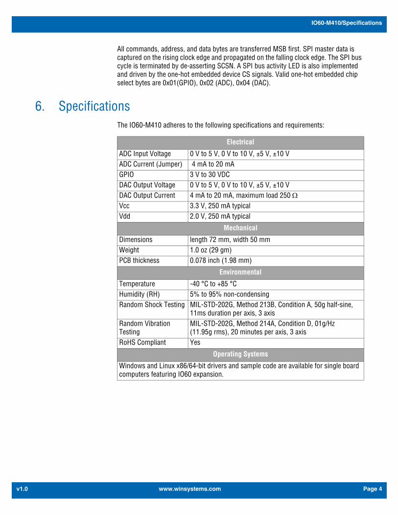
6. SpecificationsThe IO60-M410 adheres to the following specifications and requirements:
Electrical
ADC Input Voltage 0 V to 5 V, 0 V to 10 V, ±5 V, ±10 VADC Current (Jumper) 4 mA to 20 mAGPIO 3 V to 30 VDCDAC Output Voltage 0 V to 5 V, 0 V to 10 V, ±5 V, ±10 VDAC Output Current 4 mA to 20 mA, maximum load 250 Vcc 3.3 V, 250 mA typical Vdd 2.0 V, 250 mA typical
Mechanical
Dimensions length 72 mm, width 50 mmWeight 1.0 oz (29 gm)PCB thickness 0.078 inch (1.98 mm)
Environmental
Temperature -40 °C to +85 °CHumidity (RH) 5% to 95% non-condensingRandom Shock Testing MIL-STD-202G, Method 213B, Condition A, 50g half-sine,
11ms duration per axis, 3 axisRandom Vibration Testing
MIL-STD-202G, Method 214A, Condition D, 01g/Hz (11.95g rms), 20 minutes per axis, 3 axis
RoHS Compliant Yes
Operating Systems
Windows and Linux x86/64-bit drivers and sample code are available for single board computers featuring IO60 expansion.
www.winsystems.com Page 4
IO60-M410/Configuration
v1.0
Additional Accessories
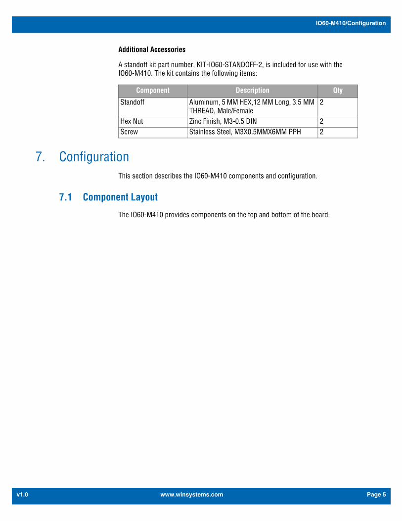
A standoff kit part number, KIT-IO60-STANDOFF-2, is included for use with the IO60-M410. The kit contains the following items:
7. ConfigurationThis section describes the IO60-M410 components and configuration.
7.1 Component Layout
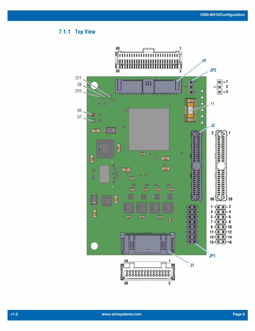
The IO60-M410 provides components on the top and bottom of the board.
Component Description Qty
Standoff Aluminum, 5 MM HEX,12 MM Long, 3.5 MM THREAD, Male/Female
2
Hex Nut Zinc Finish, M3-0.5 DIN 2Screw Stainless Steel, M3X0.5MMX6MM PPH 2
www.winsystems.com Page 5
IO60-M410/Configuration
v1.0
7.1.1 Top View
1
2
49
50
1
2
29
30
JP2
J4
F1
JP1
J2
J1
D7D6
D10
D11D8
123
12
5960
16151413121110987654321
www.winsystems.com Page 6
IO60-M410/Configuration
v1.0
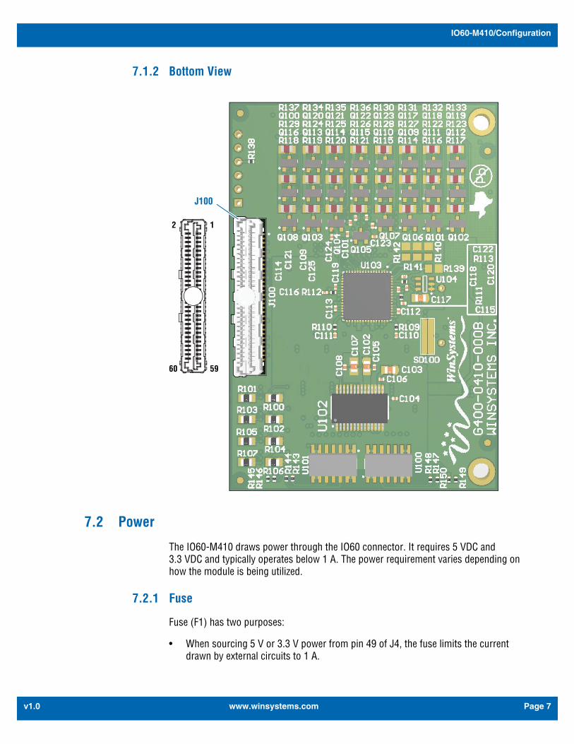
7.1.2 Bottom View
7.2 Power
The IO60-M410 draws power through the IO60 connector. It requires 5 VDC and 3.3 VDC and typically operates below 1 A. The power requirement varies depending on how the module is being utilized.
7.2.1 Fuse
Fuse (F1) has two purposes:
• When sourcing 5 V or 3.3 V power from pin 49 of J4, the fuse limits the current drawn by external circuits to 1 A.
J100
12
5960
www.winsystems.com Page 7

IO60-M410/Configuration
v1.0
• When receiving (3.3V – 30V) power on pin 49 of J4 from a user's system (for the purpose of supplying the logic level translation circuits), the fuse limits the current drawn by these circuits to 1 A.
Replace this fuse with only a fuse of the same rating: 1A,SB LITTLEFUSE (replacement part number 0454001). If the fuse repeatedly fails, correct the problem before replacing.
7.3 Embedded Computer Connection
The IO60-M410 is connected to a host embedded system through the IO60 interface (above the board through J2 or below the board through J100).
7.3.1 J2 IO60 Top Connector
Purpose: IO60 Expansion Interface Connection to host computer
Layout and Pin Reference:
Pin Name Pin Name1 VCC5 2 VCC5
3 VCC5 4 VCC5
5 TX 6 RX
7 RTS 8 CTS
9 GND 10 MUXCTRL
11 SCLK 12 MISO
13 SPI_CS0 14 MOSI
15 SPI_CS1 16 SPI_CS2
17 SPI_CS3 18 SPI_RDY
19 GND 20 GND
21 SCL 22 SDA
23 GND 24 GND
25 PWM0 26 EPITI
27 GND 28 GND
29 POR 30 GPIO_0
31 GPIO_1 32 GPIO_2
33 GPIO_3 34 GPIO_4
35 GPIO_5 36 GPIO_6
37 GPIO_7 38 NC
39 GND 40 GND
41 RSVD1 42 RSVD2
43 RSVD3 44 RSVD4
45 GND 46 GND
47 RSVD5 48 RSVD6
49 RSVD7 50 RSVD8
51 GND 52 GND
53 RSVD9 54 RSVD10
55 RSVD11 56 RSVD12
57 VCC3 58 VCC3
59 VCC3 60 VCC3
12
5960
www.winsystems.com Page 8

IO60-M410/Configuration
v1.0
Additional Information
This connection uses a Samtec LSEM-130-06.0-L-DV-A-N-K-TR connector (WinSystems part number: G650-0060-070). Same matching connector.
7.3.2 J100 IO60 Bottom Connector
Purpose: IO60 Expansion Interface Connection to host computer
Layout and Pin Reference:
Additional Information
This connection uses a Samtec LSEM-130-06.0-L-DV-A-N-K-TR connector (WinSystems part number: G650-0060-070). Same matching connector.
Pin Name Pin Name1 VCC5 2 VCC5
3 VCC5 4 VCC5
5 RX 6 TX
7 CTS 8 RTS
9 MUXCTRL 10 GND
11 MISO 12 SCLK
13 MOSI 14 SPI_CS0
15 SPI_CS2 16 SPI_CS1
17 SPI_RDY 18 SPI_CS3
19 GND 20 GND
21 SDA 22 SCL
23 GND 24 GND
25 EPITI 26 PWM0
27 GND 28 GND
29 GPIO_0 30 POR
31 GPIO_2 32 GPIO_1
33 GPIO_4 34 GPIO_3
35 GPIO_6 36 GPIO_5
37 GPIO_8 38 GPIO_7
39 GND 40 GND
41 RSVD2 42 RSVD1
43 RSVD4 44 RSVD3
45 GND 46 GND
47 RSVD6 48 RSVD5
49 RSVD8 50 RSVD7
51 GND 52 GND
53 RSVD10 54 RSVD9
55 RSVD12 56 RSVD11
57 VCC3 58 VCC3
59 VCC3 60 VCC3
12
5960
www.winsystems.com Page 9
IO60-M410/Configuration
v1.0
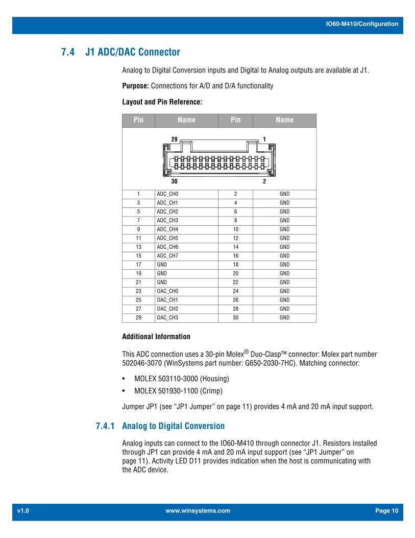
7.4 J1 ADC/DAC Connector
Analog to Digital Conversion inputs and Digital to Analog outputs are available at J1.
Purpose: Connections for A/D and D/A functionality
Layout and Pin Reference:
Additional Information
This ADC connection uses a 30-pin Molex® Duo-Clasp™ connector: Molex part number 502046-3070 (WinSystems part number: G650-2030-7HC). Matching connector:
• MOLEX 503110-3000 (Housing)
• MOLEX 501930-1100 (Crimp)
Jumper JP1 (see “JP1 Jumper” on page 11) provides 4 mA and 20 mA input support.
7.4.1 Analog to Digital Conversion
Analog inputs can connect to the IO60-M410 through connector J1. Resistors installed through JP1 can provide 4 mA and 20 mA input support (see “JP1 Jumper” on page 11). Activity LED D11 provides indication when the host is communicating with the ADC device.
Pin Name Pin Name
1 ADC_CH0 2 GND
3 ADC_CH1 4 GND
5 ADC_CH2 6 GND
7 ADC_CH3 8 GND
9 ADC_CH4 10 GND
11 ADC_CH5 12 GND
13 ADC_CH6 14 GND
15 ADC_CH7 16 GND
17 GND 18 GND
19 GND 20 GND
21 GND 22 GND
23 DAC_CH0 24 GND
25 DAC_CH1 26 GND
27 DAC_CH2 28 GND
29 DAC_CH3 30 GND
1
2
29
30
www.winsystems.com Page 10

IO60-M410/Configuration
v1.0
7.4.2 Digital to Analog Conversion
The IO60-M410 can provide Digital to Analog outputs through connector J1. Activity LED D10 provides indication when the host is communicating with the DAC device. LED D6 indicates when a DAC fault has occurred.
7.5 JP1 Jumper
The jumper at JP1 provides for 4 mA and 20 mA input support by connecting a 250 resistor across the input. This transforms a 4 mA to 20 mA current signal into a 1 V to 5 V signal to be read by the ADC. The ADC can be configured as 8 single-ended channels or 4 differential channels. If configured in differential mode, the sense resistors must be installed differently. See the following layout and pin reference for the proper settings of these jumpers for both single-ended and differential configurations.
Jumper Pin Reference:
Make sure the load is attached prior to operating the DAC in current mode. Putting the DAC into current mode and driving into an open load will cause high voltages to be generated.
Position Provides1-2 Ch0 Single Ended
3-4 Ch1 Single Ended
5-6 Ch2 Single Ended
7-8 Ch3 Single Ended
9-10 Ch4 Single Ended
11-12 Ch5 Single Ended
13-14 Ch6 Single Ended
15-16 Ch7 Single Ended
2-4 Ch0-1 Differential
6-8 Ch2-3 Differential
10-12 Ch4-5 Differential
14-16 Ch6-7 Differential
1615
1413
1211
109
87
65
43
21
www.winsystems.com Page 11
IO60-M410/Configuration
v1.0
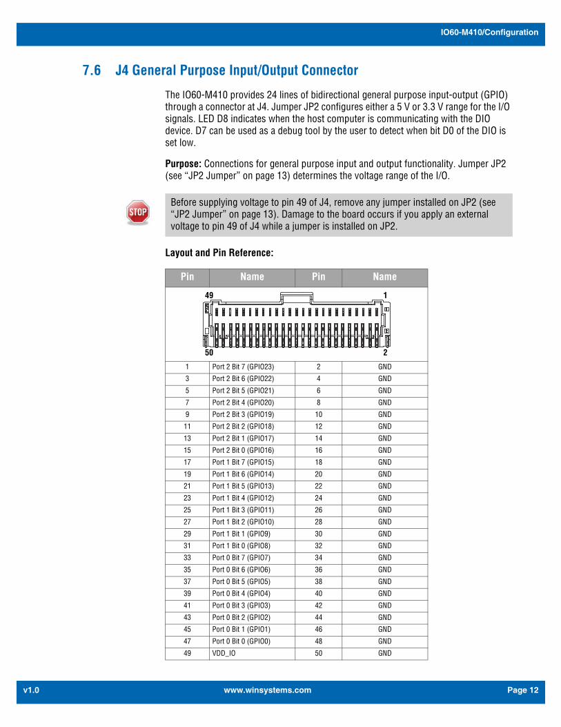
7.6 J4 General Purpose Input/Output Connector
The IO60-M410 provides 24 lines of bidirectional general purpose input-output (GPIO) through a connector at J4. Jumper JP2 configures either a 5 V or 3.3 V range for the I/O signals. LED D8 indicates when the host computer is communicating with the DIO device. D7 can be used as a debug tool by the user to detect when bit D0 of the DIO is set low.
Purpose: Connections for general purpose input and output functionality. Jumper JP2 (see “JP2 Jumper” on page 13) determines the voltage range of the I/O.
Layout and Pin Reference:
Before supplying voltage to pin 49 of J4, remove any jumper installed on JP2 (see “JP2 Jumper” on page 13). Damage to the board occurs if you apply an external voltage to pin 49 of J4 while a jumper is installed on JP2.
Pin Name Pin Name
1 Port 2 Bit 7 (GPIO23) 2 GND
3 Port 2 Bit 6 (GPIO22) 4 GND
5 Port 2 Bit 5 (GPIO21) 6 GND
7 Port 2 Bit 4 (GPIO20) 8 GND
9 Port 2 Bit 3 (GPIO19) 10 GND
11 Port 2 Bit 2 (GPIO18) 12 GND
13 Port 2 Bit 1 (GPIO17) 14 GND
15 Port 2 Bit 0 (GPIO16) 16 GND
17 Port 1 Bit 7 (GPIO15) 18 GND
19 Port 1 Bit 6 (GPIO14) 20 GND
21 Port 1 Bit 5 (GPIO13) 22 GND
23 Port 1 Bit 4 (GPIO12) 24 GND
25 Port 1 Bit 3 (GPIO11) 26 GND
27 Port 1 Bit 2 (GPIO10) 28 GND
29 Port 1 Bit 1 (GPIO9) 30 GND
31 Port 1 Bit 0 (GPIO8) 32 GND
33 Port 0 Bit 7 (GPIO7) 34 GND
35 Port 0 Bit 6 (GPIO6) 36 GND
37 Port 0 Bit 5 (GPIO5) 38 GND
39 Port 0 Bit 4 (GPIO4) 40 GND
41 Port 0 Bit 3 (GPIO3) 42 GND
43 Port 0 Bit 2 (GPIO2) 44 GND
45 Port 0 Bit 1 (GPIO1) 46 GND
47 Port 0 Bit 0 (GPIO0) 48 GND
49 VDD_IO 50 GND
1
2
49
50
www.winsystems.com Page 12

IO60-M410/Configuration
v1.0
Additional Information: This connector uses a 50-pin Molex® Pico-Clasp™ connector: Molex 501571-5007 (WinSystems part number: G650-2050-7HB). Matching connector:
• MOLEX 501189-5010 (Housing)
• MOLEX 501193-2000 (Crimp)
7.7 JP2 Jumper
The presence and position of a jumper at JP2 specifies the I/O voltage source or voltage. The voltage selected sets the upper limit for general purpose input-output (GPIO) logic level translation. If an external voltage is supplied on J4-49 then that voltage must not exceed 30 VDC and no jumpers should be installed on JP2. In position 2-3, 5 V IO is selected. In position 1-2, 3.3 V IO is selected. When the jumper is removed and the user supplies VIN <30 V on pin 49 of J4, VIN IO becomes the maximum range of the IO signals.
Purpose: Determining voltage for General Purpose Input-Output (GPIO)
Jumper Pin Reference:
Pin Reference:
Jumper Voltage source1-2 3.3 V
2-3 5 V
open External voltage supplied to Pin 49 of J4 (see STOP below)
Before supplying voltage to pin 49 of J4, remove any jumper installed on JP2. Damage to the board occurs if you apply an external voltage to pin 49 of J4 while a jumper is installed on JP2.
Pin Function1 +3.3 V
2 VDD_IO
3 +5 V
1
2
3
www.winsystems.com Page 13

IO60-M410/GPIO Registers
v1.0
7.8 LED indicators
8. GPIO Registers
8.1 Functional Description
The IO60-M410 programmable logic device implements 24 bits of 30 V tolerant General Purpose Input-Output (GPIO). The 24-bit GPIO interface is organized as a single port comprised of three 8-bit registers. Each bit of each port is individually configurable as an input or output. Additionally, the general purpose I/O may be pulled up to the system 3.3 V, 5 V, or optionally to an external user supplied voltage (VCC1). This extends the range of signal levels that can be interfaced to the port.
All commands, address, and data bytes are transferred MSB first. SPI master data is captured on the rising clock edge and propagated on the falling clock edge. The SPI bus cycle is terminated by de-asserting SCSN. A SPI bus activity LED is also implemented
VDD33
10K
5V
3V
DIO [0..23]IO [0..23]
D S
G
LED DescriptionD6 Indicates when a DAC fault has occurred.
D7 GPIO debug LED lights when bit D0 (of the DIO) is driven low.
D8 GPIO activity LED lights when a SPI transaction to the DIO occurs.
D10 Indicates when the host is communicating with the DAC device.
D11 Indicates when the host is communicating with the ADC device.
D7D6
D10
D11D8
www.winsystems.com Page 14
IO60-M410/GPIO Registers
v1.0
and driven by the one-hot embedded device CS signals. Valid one-hot embedded chip select bytes are 0x01(GPIO), 0x02 (ADC), 0x04 (DAC).
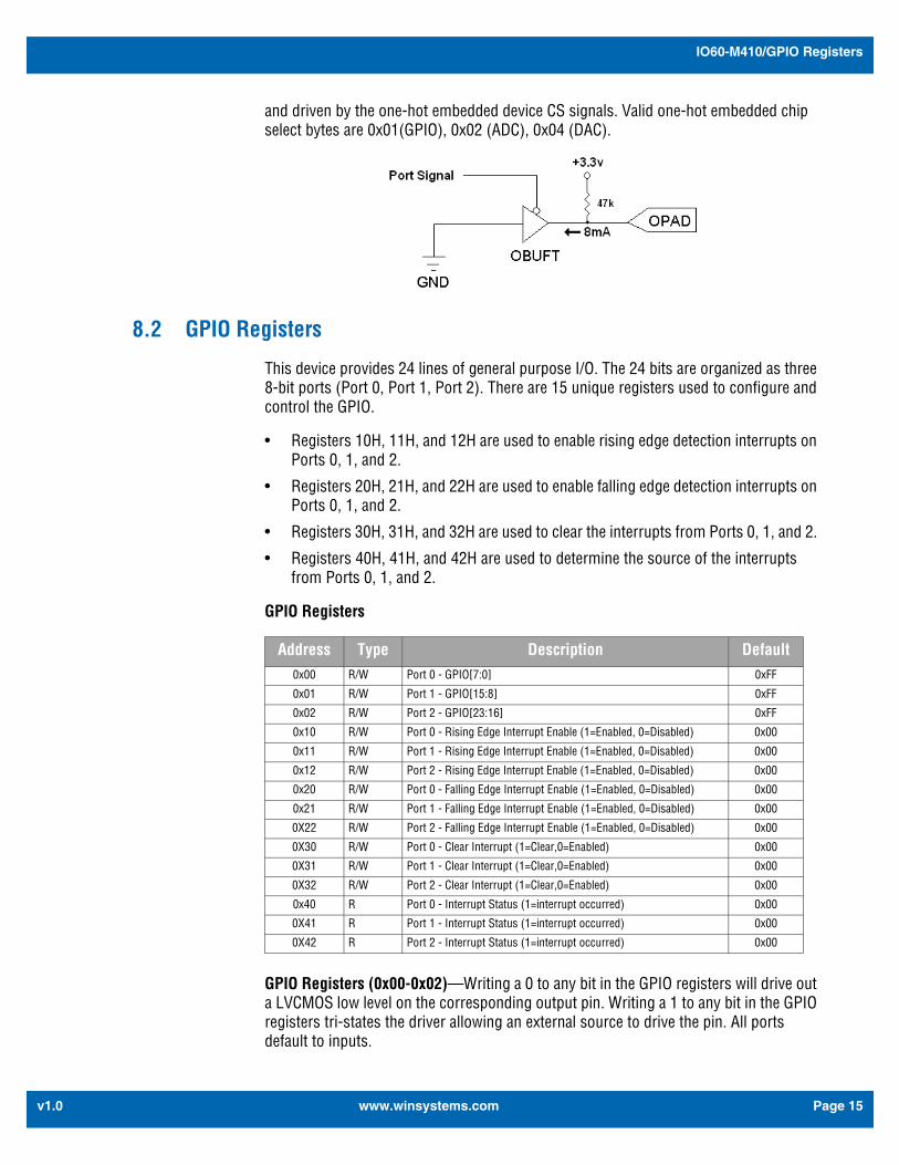
8.2 GPIO Registers
This device provides 24 lines of general purpose I/O. The 24 bits are organized as three 8-bit ports (Port 0, Port 1, Port 2). There are 15 unique registers used to configure and control the GPIO.
• Registers 10H, 11H, and 12H are used to enable rising edge detection interrupts on Ports 0, 1, and 2.
• Registers 20H, 21H, and 22H are used to enable falling edge detection interrupts on Ports 0, 1, and 2.
• Registers 30H, 31H, and 32H are used to clear the interrupts from Ports 0, 1, and 2.
• Registers 40H, 41H, and 42H are used to determine the source of the interrupts from Ports 0, 1, and 2.
GPIO Registers
GPIO Registers (0x00-0x02)—Writing a 0 to any bit in the GPIO registers will drive out a LVCMOS low level on the corresponding output pin. Writing a 1 to any bit in the GPIO registers tri-states the driver allowing an external source to drive the pin. All ports default to inputs.
Address Type Description Default0x00 R/W Port 0 - GPIO[7:0] 0xFF
0x01 R/W Port 1 - GPIO[15:8] 0xFF
0x02 R/W Port 2 - GPIO[23:16] 0xFF
0x10 R/W Port 0 - Rising Edge Interrupt Enable (1=Enabled, 0=Disabled) 0x00
0x11 R/W Port 1 - Rising Edge Interrupt Enable (1=Enabled, 0=Disabled) 0x00
0x12 R/W Port 2 - Rising Edge Interrupt Enable (1=Enabled, 0=Disabled) 0x00
0x20 R/W Port 0 - Falling Edge Interrupt Enable (1=Enabled, 0=Disabled) 0x00
0x21 R/W Port 1 - Falling Edge Interrupt Enable (1=Enabled, 0=Disabled) 0x00
0X22 R/W Port 2 - Falling Edge Interrupt Enable (1=Enabled, 0=Disabled) 0x00
0X30 R/W Port 0 - Clear Interrupt (1=Clear,0=Enabled) 0x00
0X31 R/W Port 1 - Clear Interrupt (1=Clear,0=Enabled) 0x00
0X32 R/W Port 2 - Clear Interrupt (1=Clear,0=Enabled) 0x00
0x40 R Port 0 - Interrupt Status (1=interrupt occurred) 0x00
0X41 R Port 1 - Interrupt Status (1=interrupt occurred) 0x00
0X42 R Port 2 - Interrupt Status (1=interrupt occurred) 0x00
www.winsystems.com Page 15

IO60-M410/SPI Bus
v1.0
Rising Edge Interrupt Enable Registers (0x10-0x12)—Writing a 1 to any bit in these registers enables interrupts for rising edge events on the corresponding GPIO bit. Writing a 0 disables rising edge interrupts on the same bit. The default value is all rising edge interrupts disabled.
Falling Edge Interrupt Enable Registers (0x20-0x22)—Writing a 1 to any bit in these registers enables interrupts for falling edge events on the corresponding GPIO bit. Writing a 0 disables falling edge interrupts on the same bit. The default value is all falling edge interrupts disabled.
Interrupt Clear Registers (0x30-0x32)—Writing a 0 to any bit in these registers clears the corresponding status register bit and disables the interrupts from the corresponding GPIO pin. Writing a 1 to the same bit then re-enables interrupts for the corresponding channel.
Interrupt Status Registers (0x40-0x42)—These are read only registers. If a bit is set it indicates that the corresponding channel has caused an interrupt.
9. SPI Bus
9.1 Component
The Lattice Semiconductors LCMXO2-4000HC is used on this board to implement a SPI slave to GPIO24 function. This device is part of the MACH XO2 family of PLDs with EFB (Embedded Function Blocks) and is scalable from 4000-N LUTs in a pin compatible BGA256 package.
9.2 Features
The PLD provides the system programmer an interface to any combination of 24 discrete digital inputs or outputs. Each GPIO signal is implemented as a bidirectional
www.winsystems.com Page 16
IO60-M410/SPI Bus
v1.0
open drain type output with a weak pull-up resistor. The GPIO signal pin sinks the net low (8mA) when a binary "0" is written to the port and is tri-stated and pulled to 3.3V through a weak 50K pull-up resistor when a binary "1" is written to the port. When the GPIO pin is tri-stated the pin functions as an input and the level is controlled by external system logic. When configured as an input or output a physical interrupt can be generated from the rising edge, falling edge, or both edges of any individual GPIO signal. Additionally, the PLD decodes an in-band one-hot embedded chip select byte and generates a chip select signal for either the on-chip 24bit SPI GPIO logic block, the external on-board ADC, or the external on-board DAC.
9.3 SPI Commands
The following table contains supported Serial Peripheral Interface (SPI) commands.
Write REG Command—The Write REG command is a four byte command. The first byte is the chip select byte. The second byte is the Command ID 0x01. The third byte is the register address (0x00-0x19). The fourth and last byte is the Write Data.
Read REG Command—The Read REG command is a five byte command. The first byte is the chip select byte. The second byte is the Command ID 0x05. The third byte is the
Operation Command Address byte Stuffing byte Data byteWRITE REG 0x01 1 - 1
READ REG 0x05 1 1 1
READ REVID 0x9F - 1 1
www.winsystems.com Page 17
IO60-M410/Other Registers
v1.0
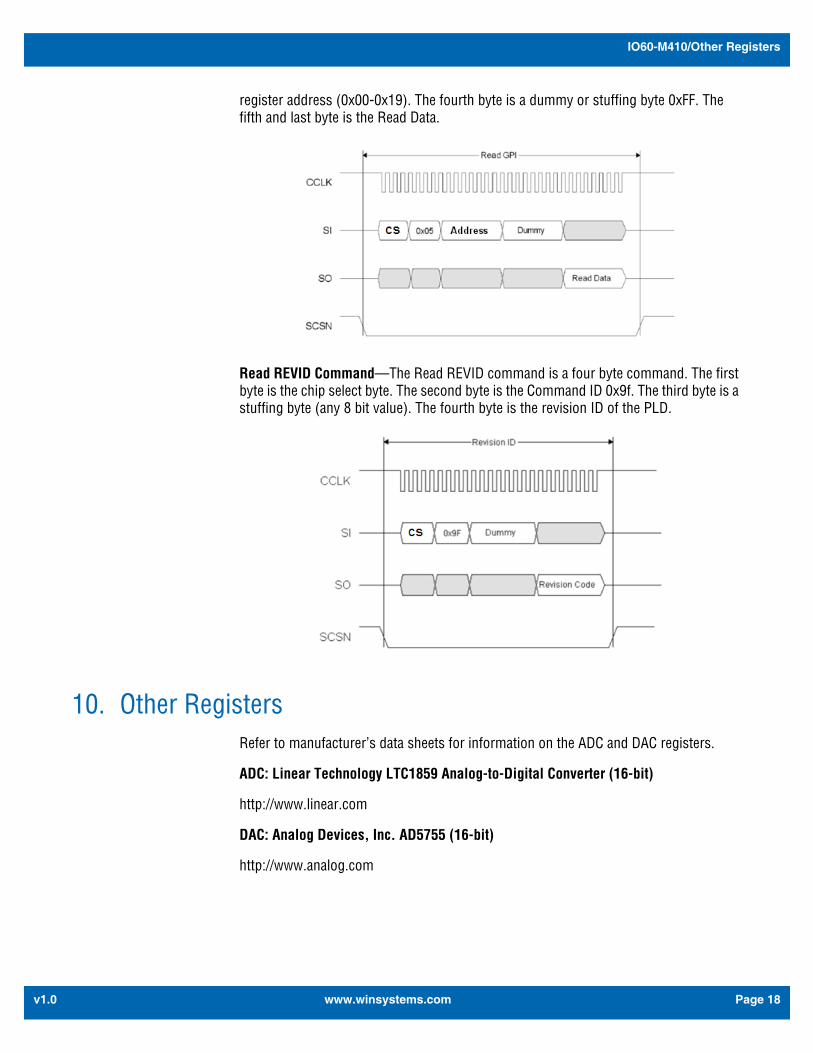
register address (0x00-0x19). The fourth byte is a dummy or stuffing byte 0xFF. The fifth and last byte is the Read Data.
Read REVID Command—The Read REVID command is a four byte command. The first byte is the chip select byte. The second byte is the Command ID 0x9f. The third byte is a stuffing byte (any 8 bit value). The fourth byte is the revision ID of the PLD.
10. Other RegistersRefer to manufacturer’s data sheets for information on the ADC and DAC registers.
ADC: Linear Technology LTC1859 Analog-to-Digital Converter (16-bit)
http://www.linear.com
DAC: Analog Devices, Inc. AD5755 (16-bit)
http://www.analog.com
www.winsystems.com Page 18

IO60-M410/Best Practices
v1.0
Appendix A. Best PracticesThe following sections outline the best practices for operating the IO60-M410 in a safe, effective manner, that will not damage the board. Please read this section carefully.
4 mA to 20 mA Current Loops
When using the ADC's jumperable shunt resistors to transform a 4 mA to 20 mA current input into a 1 V to 5 V signal (see “JP1 Jumper” on page 11), you have a choice of where in the loop to install the 249 shunt resistor. When choosing the low return net of the loop to connect the channel shunt resistance the 4 mA to 20 mA loop current will produce a signal with the following characteristics:
• VIL = 1 V
• VIH = 5 V
If connecting in the high source net of the loop, the same loop current will produce a signal with the following characteristics:
• VIL = Vsource - 4 V
• VIH = Vsource
If you choose to connect using the high source side of the loop, limit the source voltage below 10 VDC. The safest connection to a 4 mA to 20 mA loop is always in the low return net loop.
Power Down
Make sure that power has been removed from the system before making or breaking any connections.
I/O Connections OFF—I/O Connections should also be off before connecting them to the embedded computer modules or any I/O cards. Connecting hot signals can cause damage whether the embedded system is powered or not.
Avoid Electrostatic Discharge (ESD)—Only handle the circuit board and other bare electronics when electrostatic discharge (ESD) protection is in place. Having a wrist strap and a fully grounded workstation is the minimum ESD protection required before the ESD seal on the product bag is broken.
Power Supply OFF—The power supply should always be off before it is connected to the I/O Module.
www.winsystems.com Page 19
IO60-M410/Best Practices
v1.0
Mounting and Protecting the I/O Module
The IO60-M410 must be mounted properly to avoid damage.
You can order additional standoff kits from WinSystems, part number KIT-IO60-STANDOFF-2. The kit contains the following items:
Do Not Bend or Flex the I/O Module—Never bend or flex the embedded computer module. Bending or flexing can cause irreparable damage. Embedded computer modules are especially sensitive to flexing or bending around Ball-Grid-Array (BGA) devices. BGA devices are extremely rigid by design and flexing or bending the embedded computer module can cause the BGA to tear away from the printed circuit board.
Mounting Holes—The mounting holes are plated on the top, bottom and through the barrel of the hole and are connected to the embedded computer module’s ground plane. Traces are often routed in the inner layers right below, above or around the mounting holes.
• Never use a drill or any other tool in an attempt to make the holes larger.
• Never use screws with oversized heads. The head could come in contact with nearby components causing a short or physical damage.
• Never use self-tapping screws; they will compromise the walls of the mounting hole.
• Never use oversized screws that cut into the walls of the mounting holes.
• Always use all of the mounting holes. By using all of the mounting holes you will provide the support the embedded computer module needs to prevent bending or flexing.
Plug or Unplug Connectors Only on Fully Mounted Boards—Never plug or unplug connectors on a board that is not fully mounted. Many of the connectors fit rather tightly and the force needed to plug or unplug them could cause the embedded computer module to be flexed.
Avoid cutting of the I/O Module—Never use star washers or any fastening hardware that will cut into the I/O module.
Avoid Over-tightening of Mounting Hardware—Causing the area around the mounting holes to compress could damage interlayer traces around the mounting holes.
Use Appropriate Tools—Always use tools that are appropriate for working with small hardware. Large tools can damage components around the mounting holes.
Component Description Qty
Standoff Aluminum, 5 MM HEX,12 MM Long, 3.5 MM THREAD, Male/Female
2
Hex Nut Zinc Finish, M3-0.5 DIN 2Screw Stainless Steel, M3X0.5MMX6MM PPH 2
www.winsystems.com Page 20

IO60-M410/Best Practices
v1.0
Avoid Conductive Surfaces—Never allow the embedded computer module to be placed on a conductive surface. Many embedded systems use a battery to back up the clock-calendar and CMOS memory. A conductive surface such as a metal bench can short the battery causing premature failure.
Conformal Coating
Applying conformal coating to a WinSystems product will not in itself void the product warranty, if it is properly removed prior to return. Coating may change thermal characteristics and impedes our ability to test, diagnose, and repair products. Any coated product sent to WinSystems for repair will be returned at customer expense and no service will be performed.
Operations/Product Manuals
Every single board computer has an Operations manual or Product manual.
Periodic Updates—Operations/Product manuals are updated often. Periodically check the WinSystems website (http://www.winsystems.com) for revisions.
Check Pinouts—Always check the pinout and connector locations in the manual before plugging in a cable. Many I/O modules will have identical headers for different functions and plugging a cable into the wrong header can have disastrous results.
Contact an Applications Engineer—If a diagram or chart in a manual does not seem to match your board, or if you have additional questions, contact a WinSystems Applications Engineer at: +1-817-274-7553.
www.winsystems.com Page 21
IO60-M410/Mechanical Drawing
v1.0
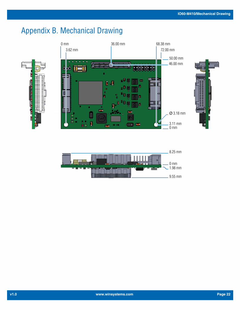
Appendix B. Mechanical Drawing0 mm 36.00 mm
3.62 mm68.38 mm
72.00 mm
0 mm
1.98 mm0 mm
9.55 mm
8.25 mm
50.00 mm
3.11 mm
Ø 3.18 mm
46.00 mm
www.winsystems.com Page 22

IO60-M410/Warranty Information
v1.0
Appendix C. Warranty InformationWinSystems warrants that for a period of two (2) years from the date of shipment, any Products and Software purchased or licensed hereunder which have been developed or manufactured by WinSystems shall be free of any defects and shall perform substantially in accordance with WinSystems' specifications therefor. With respect to any Products or Software purchased or licensed hereunder which have been developed or manufactured by others, WinSystems shall transfer and assign to Customer any warranty of such manufacturer or developer held by WinSystems, provided that the warranty, if any, may be assigned. The sole obligation of WinSystems for any breach of warranty contained herein shall be, at its option, either (i) to repair or replace at its expense any materially defective Products or Software, or (ii) to take back such Products and Software and refund the Customer the purchase price and any license fees paid for the same. Customer shall pay all freight, duty, broker's fees, insurance, charges and other fees and charges for the return of any Products or Software to WinSystems under this warranty. WinSystems shall pay freight and insurance charges for any repaired or replaced Products or Software thereafter delivered to Customer within the United States. All fees and costs for shipment outside of the United States shall be paid by Customer. The foregoing warranty shall not apply to any Products or Software which have been subject to abuse, misuse, vandalism, accident, alteration, neglect, unauthorized repair or improper installation.
THERE ARE NO WARRANTIES BY WINSYSTEMS EXCEPT AS STATED HEREIN. THERE ARE NO OTHER WARRANTIES EXPRESS OR IMPLIED INCLUDING, BUT NOT LIMITED TO, THE IMPLIED WARRANTIES OF MERCHANTABILITY AND FITNESS FOR A PARTICULAR PURPOSE. IN NO EVENT SHALL WINSYSTEMS BE LIABLE FOR CONSEQUENTIAL, INCIDENTAL OR SPECIAL DAMAGES FOR LOSS OF DATA, PROFITS OR GOODWILL. WINSYSTEMS' MAXIMUM LIABILITY FOR ANY BREACH OF THIS AGREEMENT OR OTHER CLAIM RELATED TO ANY PRODUCTS, SOFTWARE, OR THE SUBJECT MATTER HEREOF, SHALL NOT EXCEED THE PURCHASE PRICE OR LICENSE FEE PAID BY CUSTOMER TO WINSYSTEMS FOR THE PRODUCTS OR SOFTWARE OR PORTION THEREOF TO WHICH SUCH BREACH OR CLAIM PERTAINS.
Title to the Products shall remain vested in WinSystems until complete payment is made by Customer. Title to any Software shall remain vested in WinSystems, or WinSystems' licensor from whom WinSystems has obtained marketing rights, both before, during and after the term of the License. Nonpayment when due of the purchase price for any Products or the License fees for any Software, or, if applicable, taxes and/or the cost of any freight and insurance for any Products and/or Software, shall entitle WinSystems to take possession of the Products and/or Software without notice to Customer or prejudice to WinSystems' rights under contract or any other legal remedy.
Until title to the Products pass in accordance with the provision set out above, except with the prior written approval of WinSystems, no Products shall be modified, altered, moved or in any way assigned, sublet, mortgaged or charged nor may Customer part with possession of all or part of the same.
There are no understandings, agreements or representations, express or implied, other than those set forth herein. This Order embodies the entire agreement between the parties and may be waived, amended or supplemented only by a written instrument executed jointly by WinSystems and Customer as evidenced only by the signature of duly authorized officers of each party. The foregoing terms and conditions of any order which may be issued by Customer for the purchase of Products or licensing of Software hereunder.
In the event this Order is placed in the hands of an attorney or collection agency by WinSystems to collect any sums due hereunder to WinSystems, Customer shall pay all reasonable attorney's fees, expenses, collection and court costs incurred by WinSystems.
THIS AGREEMENT SHALL BE GOVERNED AND CONSTRUED UNDER THE TEXAS UNIFORM COMMERCIAL CODE AND THE APPLICABLE LAWS OF THE STATE OF TEXAS. THE PARTIES ACKNOWLEDGE THAT ANY ACTION BROUGHT HEREUNDER SHALL ONLY BE BROUGHT IN A COURT OF COMPETENT JURISDICTION IN TARRANT COUNTY, TEXAS.
Warranty Service
1. To obtain service under this warranty, obtain a return authorization number. In the United States, contact the WinSystems' Service Center for a return authorization number. Outside the United States, contact your local sales agent for a return authorization number.
2. You must send the product postage prepaid and insured. You must enclose the products in an anti-static bag to protect from damage by static electricity. WinSystems is not responsible for damage to the product due to static electricity.
www.winsystems.com Page 23


![Index [application.wiley-vch.de]digital memory 114 digital mirror device 215 digital MOS circuit 53 digital power management 485 digital products 568 digital signal 55 digital technology](https://static.fdocuments.us/doc/165x107/5f08ef357e708231d4246eeb/index-digital-memory-114-digital-mirror-device-215-digital-mos-circuit-53-digital.jpg)