INVITED PAPER TechnologiesforCofabricating MEMSandElectronics
526IEICE TRANS. ELECTRON., VOL.E104–C, NO.10 OCTOBER 2021
INVITED PAPER Special Section on Microwave and Millimeter-Wave Technologies
Overview and Prospects of High Power Amplifier Technology Trendfor 5G and beyond 5G Base Stations
Koji YAMANAKA†a), Shintaro SHINJO†, Senior Members, Yuji KOMATSUZAKI†, Shuichi SAKATA†,Keigo NAKATANI†, and Yutaro YAMAGUCHI†, Members
SUMMARY High power amplifier technologies for base transceiverstations (BTSs) for the 5th generation (5G) mobile communication sys-tems and so-called beyond 5G (B5G) systems are reviewed. For sub-6, which is categorized into frequency range 1 (FR1) in 5G, widebandDoherty amplifiers are introduced, and a multi-band load modulation am-plifier, an envelope tracking amplifier, and a digital power amplifier forB5G are explained. For millimeter wave 5G, which is categorized into fre-quency range 2 (FR2), GaAs and GaN MMICs operating at around 28GHzare introduced. Finally, future prospect for THz GaN devices is described.key words: 5G, beyond 5G, high power amplifier, base-station, Dohertyamplifier, digital power amplifier
1. Introduction
In 2019, the 5th generation mobile communication (5G) ser-vice has started in Korea, United States, and other countries.In Japan, 5G started in March 2020. In 5G systems, themaximum data transmission rate is upgraded up to 20 Gbps,which is roughly 20 times higher than that of the 4th gen-eration mobile telecommunication (4G) systems. The max-imum number of devices connected in a certain area is alsoextended to 1,000,000 devices/km2, which is 10 times largerthan that of 4G, and access delay (latency) is shortened to1ms, which is 1/10 of that of 4G. In addition, the next gen-eration system, which is called beyond 5G (B5G) or 6G, hasstarted to be discussed in the world [1], [2]. In B5G, a fur-ther higher maximum data rate, a further larger number ofconnected devices, and further lower latency are expected.
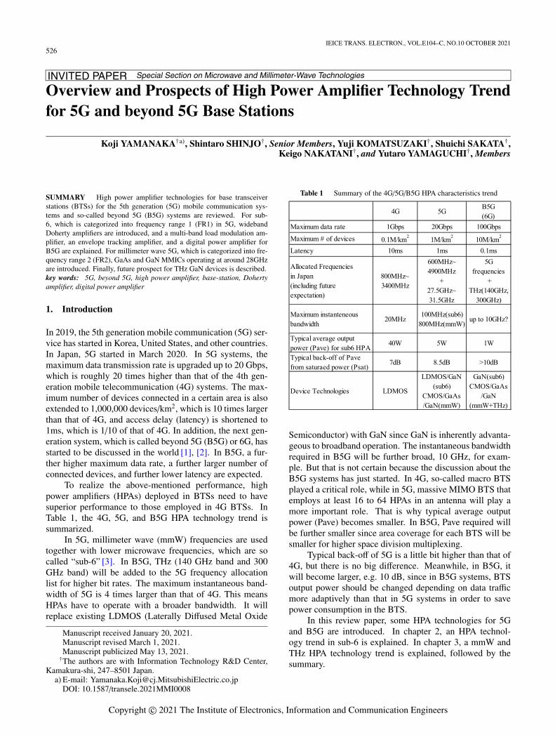
To realize the above-mentioned performance, highpower amplifiers (HPAs) deployed in BTSs need to havesuperior performance to those employed in 4G BTSs. InTable 1, the 4G, 5G, and B5G HPA technology trend issummarized.
In 5G, millimeter wave (mmW) frequencies are usedtogether with lower microwave frequencies, which are socalled “sub-6” [3]. In B5G, THz (140 GHz band and 300GHz band) will be added to the 5G frequency allocationlist for higher bit rates. The maximum instantaneous band-width of 5G is 4 times larger than that of 4G. This meansHPAs have to operate with a broader bandwidth. It willreplace existing LDMOS (Laterally Diffused Metal Oxide
Manuscript received January 20, 2021.Manuscript revised March 1, 2021.Manuscript publicized May 13, 2021.†The authors are with Information Technology R&D Center,
Kamakura-shi, 247–8501 Japan.a) E-mail: [email protected]
DOI: 10.1587/transele.2021MMI0008
Table 1 Summary of the 4G/5G/B5G HPA characteristics trend
Semiconductor) with GaN since GaN is inherently advanta-geous to broadband operation. The instantaneous bandwidthrequired in B5G will be further broad, 10 GHz, for exam-ple. But that is not certain because the discussion about theB5G systems has just started. In 4G, so-called macro BTSplayed a critical role, while in 5G, massive MIMO BTS thatemploys at least 16 to 64 HPAs in an antenna will play amore important role. That is why typical average outputpower (Pave) becomes smaller. In B5G, Pave required willbe further smaller since area coverage for each BTS will besmaller for higher space division multiplexing.
Typical back-off of 5G is a little bit higher than that of4G, but there is no big difference. Meanwhile, in B5G, itwill become larger, e.g. 10 dB, since in B5G systems, BTSoutput power should be changed depending on data trafficmore adaptively than that in 5G systems in order to savepower consumption in the BTS.
In this review paper, some HPA technologies for 5Gand B5G are introduced. In chapter 2, an HPA technol-ogy trend in sub-6 is explained. In chapter 3, a mmW andTHz HPA technology trend is explained, followed by thesummary.
Copyright c© 2021 The Institute of Electronics, Information and Communication Engineers

YAMANAKA et al.: OVERVIEW AND PROSPECTS OF HIGH POWER AMPLIFIER TECHNOLOGY TREND FOR 5G AND BEYOND 5G BASE STATIONS527
2. HPA Technology Trend in sub6 GHz
In Fig. 1, the BTS HPA technology trend is shown schemat-ically [4]. Doherty amplifier technology has been used since3G, and most of BTS HPAs in sub-6 are still based onthe Doherty amplifier technology. Although the conven-tional analogue Doherty amplifiers are advantageous to en-hance back-off efficiency for around 6 dB back-off, it isnot suitable for wide-band operation since the conventionalanalogue Doherty amplifiers usually employ quarter wave-length transmission lines. An optimum back-off power levelfor efficiency enhancement can be tuned by changing theoutput power ratio of a carrier (or main) amplifier to apeak (or auxiliary) amplifier. However, as the optimumback-off level goes up over 6 dB, the modulation-signal-based efficiency in the analogue Doherty amplifiers suffersfrom a relative large dip of efficiency observed in betweenthe optimum back-off power level and the saturation powerlevel. Moreover, an operation bandwidth for the Dohertyamplifiers becomes narrower as the output power ratio be-comes larger. To address these problems, some new types ofDoherty amplifiers have been proposed to date [5]–[13]. Forefficiency enhancement at arbitrary back-off levels, GaNenvelope tracking (ET) amplifiers have already been pro-posed [14], [15]. It has long been considered that ET ampli-fier is NOT suitable for BTS HPAs. Although high-voltageand large-current operation is required for the BTS HPAs,it was not easy for envelope amplifiers to handle such highvoltage and high current. However, by using GaN for bothan RF amplifier and an envelope amplifier, an ET BTS HPAhas become realistic. As the need for the arbitrary back-offoperation becomes more important, it is considered that adigital controlled transmitter with a switching amplifier willbe employed finally.
In Fig. 2, the photo of a wideband GaN Doherty poweramplifier with a frequency dependency compensating cir-cuit (FDCC) is shown [5]. As mentioned before, the con-ventional Doherty amplifiers are not good at wideband
Fig. 1 BTS HPA technology trend in sub6 GHz [4]
operation, because a quarter wave-length transmission lineconnected to the output of main amplifier limits the oper-ational bandwidth. The Doherty amplifier shown in Fig. 2features a novel FDCC that consists of a half wave-lengthtransmission line attached to the output of the peak am-plifier. This FDCC compensates for the parasitic reac-tance generated by the quarter wave-length transmission.Measured frequency dependences of drain efficiency (DE)and output power with ACLR using a digital predistortion(DPD) are shown in Fig. 3 [5], where DE and output powerat ACLR < −50 dBc are plotted. Thanks to the FDCC, morethan 34.3 dBm of output power and more than 45% of DEare successfully obtained over a 400 MHz operational band-width. This is well enough to cover 4 channels of a 5G newradio (NR) 100 MHz signal bandwidth.
To employ the Doherty amplifier configuration shownin Fig. 2 in realistic massive-MIMO 5G antennas, the cir-cuit area occupied by the amplifier should be miniaturizedto far less than unit antenna separation, typically 30 mm.The photo of the fully-integrated 2 stage GaN Dohertypower amplifier module with a compact FDCC is shownin Fig. 4 [16]. Matching circuits consist of lumped elementchip capacitors, chip inductors, and transmission lines fabri-cated on a laminate. The module size is as small as 10 mm x6 mm. Performance of the module with a compact FDCC
Fig. 2 Photo of wideband GaN Doherty power amplifier with frequencydependency compensating circuit (FDCC) [5]
Fig. 3 Measured frequency dependences of DE and output power withACLR of −50 dBc with DPD [5]

528IEICE TRANS. ELECTRON., VOL.E104–C, NO.10 OCTOBER 2021
Fig. 4 Photo of the fully-integrated 2-stage GaN Doherty power ampli-fier module with a compact FDCC (a) before molding and (b) after mold-ing [16]
Fig. 5 Performance of the 2-stage GaN DPA Module with a compactFDCC after molding [16]
after molding is shown in Fig. 5 [16]. More than 37.5 dBmoutput power and 43% power added efficiency (PAE) areobtained over 3.4 to 3.8 GHz, which is globally used for 5Gsub-6 applications.
The Doherty power amplifier module shown in Fig. 4 iswell enough for the early stage of 5G. However, in the laterstage of 5G or in the B5G era, it is considered that multiplespectrums in both 4G and 5G will be used to enhance thespectral efficiency. To fulfil the condition, BTS amplifiersshould be able to operate in every frequency band of 4G and5G. In the case of Japan, 800 MHz to 4.9 GHz operation (in-cluding so-called local 5G) is required for the BTS ampli-fiers. To realize such broadband operation fully a new-typeload modulation amplifier is proposed.
In Fig. 6, photo of a frequency-periodic load modulatedGaN power amplifier is shown [17]. In Fig. 7, measured fre-quency dependences of drain efficiency and output power at6 dB power back-off level are shown [17]. The amplifier isnot a conventional load modulated amplifier, but a dual in-put load modulated amplifier. By controlling the power ratioof the two inputs (RFin1 and RFin2) and phase differencebetween RFin1 and RFin2, periodic occurrence of Dohertyamplifier operation and outphasing amplifier operation is re-alized. By doing so, more than 30 dBm output power andmore than 45% drain efficiency is obtained over 1.4 GHzto 4.8 GHz. This is not enough to fully cover 800 MHz to4900 MHz range. But, most of the 4G and 5G frequency
Fig. 6 Photo of a frequency-periodic load modulated GaN power ampli-fier [17]
Fig. 7 Measured frequency dependences of drain efficiency and outputpower at 6 dB power back-off level [17]
Fig. 8 Circuit diagram of the soft-switching buck-converter and chipphoto [14]

YAMANAKA et al.: OVERVIEW AND PROSPECTS OF HIGH POWER AMPLIFIER TECHNOLOGY TREND FOR 5G AND BEYOND 5G BASE STATIONS529
Fig. 9 Measured PAE vs. output power of RF amplifier for ET at 3.6 GHzwith various fixed power supply voltages [14] Conversion efficiency ofbuck-converter is not included.
Fig. 10 Schematic of a CMOS/GaN digital power amplifier [18]
bands are covered.The circuit diagram of the soft-switching buck-
converter and GaN chip photo employed in the GaN ETamplifier are shown in Fig. 8 [14]. By using a GaN-basedbuck-converter configuration, high power and high conver-sion efficiency are realized simultaneously [15]. Moreover,with the resonance of parasitic capacitance and inductance,the current waveform is switched on and off softly, therebyresulting in the great reduction in switching noise withoutsacrificing efficiency. In Fig. 9, measured PAE vs. outputpower of RF amplifier for ET amplifier at 3.6 GHz is shownas a parameter of power supply voltage [14]. Conversion ef-ficiency of buck-converter is not included. What is worthnoticeable is that maximum drain efficiency is almost con-stant for power supplies ranging from 10 V to 30 V. Overalmost 10 dB output power dynamic range, the drain effi-ciency is quite high and flat. It means that even in more than10 dB back-off condition that is probably required for B5GBTSs, this amplifier can operate with high efficiency.
It is considered that the ultimate circuit configura-tion for BTS HPA is a digital switching amplifier sinceit is highly efficient and highly flexible at the same
Fig. 11 A spectrum with a full span of 2.5 GHz for the carrier frequen-cies of 500 MHz, 1.6016 GHz, and 1.9219 GHz with a bandwidth of18.75 MHz [21]
time [18]–[20]. One of such digital switching amplifiers isshown in Fig. 10 [18]. It uses a GaN FET connected with asilicon CMOS digital power amplifier. The CMOS digitalpower amplifier is capable of producing any kind of modu-lation signal at any frequency within transistor’s transitionfrequency (Ft), but output power is small. Meanwhile, aGaN FET is capable of handling high power. By driving theGaN FET with the CMOS digital power amplifier, digitalHPA operation is realized.
One of the benefits of employing DPA is generation ofmulti-tone signals. One example of an FPGA (Field Pro-grammable Gate Array)-based all-digital RF transmitter isshown in Fig. 11 [21]. Three carrier signals at 500 MHz,1.6 GHz and 1.92 GHz are generated.
3. HPA Technology Trend in Millimeter-Wave
As is mentioned in Introduction, mmW (e.g. 27.5 GHz ∼31 GHz) is also used in 5G. 5G mmW BTS is classified intothe following three categories; (a) short range BTS that isused for in-room or spot area high speed wireless connec-tions, where EIRP (Equivalent Isotropic Radiation Power)is, e.g. 45 dBm. (b) Middle range BTS for last one mileconnection or FWA (Fixed Wireless Access), where EIRPis, e.g. 60 dBm. (c) Long range BTS which is used for wire-less back-haul connections, where EIRP is, e.g. 70 dBm. Tothe short range BTS, an integrated silicon RF-IC [22], [23]solution will be advantageous since it is generally low cost.For the middle range BTS, a GaAs MMIC solution can beused since output power of GaAs MMICs is 10 dB to 15 dBhigher than that of silicon RF-ICs [24]–[26]. One exampleof GaAs MMIC frontend modules (FEMs) operating in a28 GHz band is shown in Fig. 12 [24]. A massive MIMOantenna, which consists of 64 RF FEMs shown in Fig. 12exhibits a maximum data transmission rate of 25.5 Gbps.
For the long range BTSs, a GaN solution will be morelikely to be used because its output power is far higher thanthat of silicon RF-IC or GaAs MMIC. One example of GaNMMIC high power amplifiers operating around 28 GHz isshown in Fig. 12 [27]. The final stage of the amplifier isDoherty configuration to enhance efficiency at a back-offcondition. Doherty operation is hard to realize at the usual

530IEICE TRANS. ELECTRON., VOL.E104–C, NO.10 OCTOBER 2021
Fig. 12 Photo of fabricated GaAs RF frontend module [24]
Fig. 13 Photograph of the GaN Doherty Amplifier MMIC [27]
Fig. 14 Measured and simulated large-signal characteristics of theMMIC amplifier under CW operation at Vd = 24 V, IdqMain = 50 mA/mmand IdqAux = 0 mA/mm. Frequency is 28.5 GHz [27]
mmW frequencies because parasitic capacitance of transis-tor prevents load modulation behavior that is essential toDoherty operation. In the amplifier shown in Fig. 13, par-asitic capacitance is cancelled with short-circuited stubs so
Fig. 15 State-of-the-art output power of GaN devices [31]
Fig. 16 Estimated Ft, Fmax and Foperate for short gate GaN FET [31]
that load modulation effect is induced. Measured Pin-Pout,PAE and Gain curves are shown in Fig. 14 together with sim-ulated (or designed) curves [27]. Each curve exhibits an in-flection point at around Pin = 18 dBm, which shows a loadmodulation in Doherty amplifier configuration. PAE at sat-uration is 25% and PAE at 6 dB back-off (Pin = 15 dBm) is23%. In typical class-A amplifiers, efficiency at 6 dB back-off is one-fourth of saturation efficiency. That means theDoherty configuration successfully enhances PAE at 6 dBback-off by 17 percentage points.
Carrier frequency of BTS will be raised up to THz inthe B5G era. There have already been some reports on theTHz (over 100 GHz) operation RF-ICs [28], [29]. Somepromising results for possible THz GaN devices have alsobeen reported [30]. Figure 15 summarizes the state-of-the-art output power of GaN devices [31]. Output power tends todecrease in inverse proportion to operation frequency. How-ever, more than 5 W of output power has been reported at
YAMANAKA et al.: OVERVIEW AND PROSPECTS OF HIGH POWER AMPLIFIER TECHNOLOGY TREND FOR 5G AND BEYOND 5G BASE STATIONS531
around 100 GHz.Generally speaking, maximum oscillation frequency
(Fmax) and Ft of field effect transistors are inversely pro-portional to gate length (Lg). It is also empirically knownthat a practical maximum operating frequency (Foperate)is proportional to Fmax and Ft. In Fig. 16, Ft, Fmax, andFoperate, which are estimated from experimental results inliteratures, is shown [31]. The figure suggests that Fmax ofGaN FET will exceed 300 GHz when Lg becomes smallerthan 0.1µm.
As Lg goes down below 0.02 µm, or 20 nm, Foperatewill reach 300 GHz. Considering that a 20 nm lithographyprocess is no more special process in silicon CMOS technol-ogy, THz GaN devices deployed in B5G BTS will be likelyto appear within a decade.
4. Conclusion
HPA technology for BTS trends have been overviewed onthe basis of several published papers. In sub-6, namely be-low 6GHz 5G, small form-factor and wide-band GaN HPAmodules is used in 5G, whereas broadband HPAs that willcover 4G and 5G frequencies and envelope tracking HPAwill be used in B5G. Finally, BTS HPAs will move to dig-ital power amplifiers. In mmW operation, silicon RFICs,GaAs MMICs and GaN MMICs are used for high data rate5G BTS. Operating frequency will exceed 100 GHz in B5G,where Si RF-ICs and GaN MMICs will be used.
Acknowledgments
The authors would like to acknowledge all the people in-volved in these works, especially Prof. Peter Asbeck in Uni-versity California San Diego, Dr. Rui Ma, Dr. Koon Teo,and Dr. Phil Orlik in Mitsubishi Electric Research Labora-tory, Prof. Ilthco Angelov in Chalmers University of Tech-nology, Prof. Toshiyuki Oishi in Saga University, and Dr.Sandro Lanfranco in Nokia Bell laboratory for their contin-uous collaborations.
References
[1] https://www.oulu.fi/6gflagship/[2] https://www.nttdocomo.co.jp/english/corporate/technology/
whitepaper 6g/[3] https://www.tele.soumu.go.jp/e/index.htm[4] R. Ma, K.H. Teo, S. Shinjo, K. Yamanaka, and P.M. Asbeck, “A
GaN PA for 4G LTE-Advanced and 5G: Meeting the Telecommu-nication Needs of Various Vertical Sectors Including Automobiles,Robotics, Health Care, Factory Automation, Agriculture, Education,and More,” IEEE Microw. Mag., vol.18, no.7, pp.77–85, Nov.-Dec.2017.
[5] Y. Komatsuzaki, K. Nakatani, S. Shinjo, S. Miwa, R. Ma, and K.Yamanaka, “3.0–3.6 GHz wideband, over 46% average efficiencyGaN Doherty power amplifier with frequency dependency compen-sating circuits,” 2017 IEEE Topical Conference on RF/MicrowavePower Amplifiers for Radio and Wireless Applications (PAWR),p.22, 2017.
[6] J. Shao, R. Ma, K.H. Teo, S. Shinjo, and K. Yamanaka, “A fully ana-log two-way sequential GaN power amplifier with 40% fractional
bandwidth,” 2015 IEEE International Wireless Symposium (IWS2015), 2015.
[7] C.M. Andersson, E. Kuwata, Y. Kawamura, S. Shinjo, and K.Yamanaka, “A 0.85 – 2.7 GHz two-cell distributed GaN power am-plifier designed for high efficiency at 1-dB compression,” 2015 Eu-ropean Microwave Conference (EuMC), 2015.
[8] J. Shao, R. Ma, S. Shinjo, S. Chung, and K.H. Teo, “Design ofbroadband three-way sequential power amplifiers,” 2016 IEEE In-ternational Symposium on Radio-Frequency Integration Technology(RFIT), 2016.
[9] S. Niu, A.M. Koushik, R. Ma, K.H. Teo, S. Shinjo, and Y.Komatsuzaki, “Stochastically approximated multiobjective opti-mization of dual input digital Doherty Power Amplifier,” 2017 IEEE10th International Workshop on Computational Intelligence and Ap-plications (IWCIA), 2017.
[10] R. Ma, M. Benosman, K.A. Manjunatha, Y. Komatsuzaki, S. Shinjo,K.H. Teo, and P.V. Orlik, “Machine-Learning Based Digital Do-herty Power Amplifier,” 2018 IEEE International Symposium on Ra-dio-Frequency Integration Technology (RFIT), 2018.
[11] S. Honda, S. Sakata, Y. Komatsuzaki, and S. Shinjo, “Efficiency En-hancement of GaN Doherty Power Amplifier at Large Power Back-Offwith Virtual Short Stub Technique,” 2019 IEEE Asia-Pacific Mi-crowave Conference (APMC), 2019.
[12] S. Sakata, Y. Komatsuzaki, and S. Shinjo, “Adaptive Input-PowerDistribution in Doherty Power Amplifier using Modified WilkinsonPower Divider,” 2020 IEEE Topical Conference on RF/MicrowavePower Amplifiers for Radio and Wireless Applications (PAWR),2020.
[13] Y. Komatsuzaki, R. Ma, S. Sakata, K. Nakatani, and S. Shinjo, “ADual-Mode Bias Circuit Enabled GaN Doherty Amplifier Operatingin 0.85-2.05GHz and 2.4-4.2GHz,” 2020 IEEE/MTT-S InternationalMicrowave Symposium (IMS), 2020.
[14] Y. Komatsuzaki, S. Lanfranco, T. Kolmonen, O. Piirainen, J.K.Tanskanen, S. Sakata, R. Ma, S. Shinjo, K. Yamanaka, andP. Asbeck, “A High Efficiency 3.6-4.0 GHz Envelope-TrackingPower Amplifier Using GaN Soft-Switching Buck-Converter,” 2018IEEE/MTT-S International Microwave Symposium – IMS, p.465,2018.
[15] S. Sakata, S. Lanfranco, T. Kolmonen, O. Piirainen, T. Fujiwara,S. Shinjo, and P. Asbeck, “An 80MHz modulation bandwidth highefficiency multi-band envelope-tracking power amplifier using GaNsingle-phase buck-converter,” 2017 IEEE MTT-S International Mi-crowave Symposium (IMS), 2017.
[16] S. Sakata, K. Kato, E. Teranishi, T. Sugitani, R. Ma, K. Chuang,Y.-C. Wu, K. Fukunaga, Y. Komatsuzaki, K. Horiguchi, K.Yamanaka, and S. Shinjo, “A Fully-Integrated GaN Doherty PowerAmplifier Module with a Compact Frequency-Dependent Com-pensation Circuit for 5G massive MIMO Base Stations,” 2020IEEE/MTT-S International Microwave Symposium (IMS), p.712,2020.
[17] Y. Komatsuzaki, R. Ma, M. Benosman, Y. Nagai, S. Sakata, K.Nakatani, and S. Shinjo, “A Novel 1.4-4.8 GHz Ultra-Wideband,over 45% High Efficiency Digitally Assisted Frequency-PeriodicLoad Modulated Amplifier,” 2019 IEEE MTT-S International Mi-crowave Symposium (IMS), p.706, 2019.
[18] V. Diddi, S. Sakata, S. Shinjo, V. Vorapipat, R. Eden, and P. Asbeck,“Broadband digitally-controlled power amplifier based on CMOS /GaN combination,” 2016 IEEE Radio Frequency Integrated CircuitsSymposium (RFIC), p.258, 2016.
[19] S. Chung, R. Ma, S. Shinjo, H. Nakamizo, K. Parsons, and K.H. Teo,“Concurrent Multiband Digital Outphasing Transmitter ArchitectureUsing Multidimensional Power Coding,” IEEE Trans. Microw. The-ory Techn., vol.63, no.2, pp.598–613, 2015.
[20] S. Chung, R. Ma, S. Shinjo, K. Yamanaka, and K.H. Teo, “A concur-rent triple-band digital transmitter using feedforward noise cancel-lation for delta-sigma modulation,” 2017 12th European MicrowaveIntegrated Circuits Conference (EuMIC), 2017.

532IEICE TRANS. ELECTRON., VOL.E104–C, NO.10 OCTOBER 2021
[21] D.C. Dinis, R. Ma, S. Shinjo, K. Yamanaka, K.H. Teo, P.V.Orlik, A.S.R. Oliveira, and J. Vieira, “A Real-Time Architecturefor Agile and FPGA-Based Concurrent Triple-Band All-Digital RFTransmission,” IEEE Trans. Microw. Theory Techn., vol.66, no.11,pp.4955–4966, 2018.
[22] https://www.anokiwave.com/[23] R. McMorrow, D. Corman, and A. Crofts, “All silicon mmW planar
active antennas: The convergence of technology, applications, andarchitecture,” 2017 IEEE International Conference on Microwaves,Antennas, Communications and Electronic Systems (COMCAS),2017.
[24] S. Shinjo, K. Nakatani, J. Kamioka, R. Komaru, H. Noto,H. Nakamizo, S. Yamaguchi, S. Uchida, A. Okazaki, and K.Yamanaka, “A 28GHz-band highly integrated GaAs RF frontendModule for Massive MIMO in 5G,” 2018 IEEE MTT-S InternationalMicrowave Workshop Series on 5G Hardware and System Technolo-gies (IMWS-5G), 2018.
[25] K. Nakatani, Y. Komatsuzaki, S. Shinjo, J. Kamioka, R. Komaru,H. Nakamizo, K. Miyawaki, and K. Yamanaka, “A highly integratedRF frontend module including Doherty PA, LNA and switch for highSHF wide-band massive MIMO in 5G,” 2017 IEEE Topical Confer-ence on RF/Microwave Power Amplifiers for Radio and WirelessApplications (PAWR), 2017.
[26] S. Shinjo, K. Nakatani, K. Tsutsumi, and H. Nakamizo, “Integratingthe Front End: A Highly Integrated RF Front End for High-SHFWide-Band Massive MIMO in 5G,” IEEE Microw. Mag., vol.18,no.5, pp.31–40, July-Aug. 2017.
[27] K. Nakatani, Y. Yamaguchi, Y. Komatsuzaki, S. Sakata, S. Shinjo,and K. Yamanaka, “A Ka-Band High Efficiency Doherty Power Am-plifier MMIC using GaN-HEMT for 5G Application,” 2018 IEEEMTT-S International Microwave Workshop Series on 5G Hardwareand System Technologies (IMWS-5G), 2018.
[28] K. Takano, S. Amakawa, K. Katayama, S. Hara, R. Dong, A.Kasamatsu, I. Hosako, K. Mizuno, K. Takahashi, T. Yoshida, andM. Fujishima, “17.9 A 105Gb/s 300GHz CMOS transmitter,” 2017IEEE International Solid-State Circuits Conference (ISSCC), 2017.
[29] S. Lee, S. Hara, T. Yoshida, S. Amakawa, R. Dong, A. Kasamatsu,J. Sato, and M. Fujishima, “An 80-Gb/s 300-GHz-Band Single-ChipCMOS Transceiver,” IEEE J. Solid-State Circuits, vol.54, issue 12,pp.3577–3588, Dec. 2019. DOI: 10.1109/JSSC.2019.2944855
[30] I. Watanabe, Y. Yamashita, and A. Kasamatsu, “Research and Devel-opment of GaN-based HEMTs for Millimeter- and Terahertz-WaveWireless Communications,” 2020 IEEE International Symposiumon Radio-Frequency Integration Technology (RFIT), 2020.
[31] K. Yamanaka, T. Oishi, K. Yamauchi, H. Uchida, and E. Kuwata,“Current Status and Future Prospect of High Frequency GaN De-vices,” MWP-THz Joint Workshop, NICT, Koganei, 4th Feb. 2011.
Koji Yamanaka received his B.S. degreein electric engineering and M.S. and Ph.D. de-grees in electronic engineering from the Uni-versity of Tokyo, Japan, in 1993, 1995, and1998, respectively. In 1998, he joined the In-formation Technology Research and Develop-ment Center, Mitsubishi Electric Corporation,Kamakura, Japan, where he engaged in de-velopment of GaAs low-noise monolithic mi-crowave integrated circuit amplifiers and GaNhigh-power amplifiers. From 2012 to 2018, he
has managed the Amplifier Group, in Mitsubishi Electric Corporation. Hewas in charge of the civil application GaN device business section in from2018 to 2020. He is a senior member of IEICE. He is the recipient of theBest Paper Prize of GAAS2005.
Shintaro Shinjo received the B.S. andM.S. degrees in physics and Ph.D. degree in en-gineering from Keio University, Tokyo, Japan,in 1996, 1998, and 2011, respectively. In1998, he joined Mitsubishi Electric Corporation,Kamakura, Japan, where he has been involvedin the research and development of microwavemonolithic integrated circuits and solid-statepower amplifiers. From 2011 to 2012, hewas a visiting scholar with the University ofCalifornia at San Diego, San Diego, CA, USA.
He is a senior member of Electrical and Electronics Engineers (IEEE). Hewas a recipient of the Prize for Science and Technology (Development Cat-egory) of the Commendation for Science and Technology by the Ministerof Education, Culture, Sports, Science and Technology in 2009 and theIEICE Electronics Society Award in 2011.
Yuji Komatsuzaki received the B.Sc.,M.Sc. and Ph.D. degrees in electrical engineer-ing from Waseda University, Tokyo, Japan, in2007, 2009 and 2012, respectively. Since 2012,he has been with the Information TechnologyResearch and Development Center, MitsubishiElectric Corporation, Kamakura, Japan, wherehe has been involved with the research and de-velopment of microwave amplifiers for telecom-munication systems. From 2016 to 2017, he wasa visiting scholar with the Center for Wireless
Communication, University of California, San Diego.
Shuichi Sakata received the B.S. degreein Materials Engineering, and M.S. and Ph.D.degree in Electrical Engineering from the Uni-versity of Tokyo, Tokyo, Japan, in 2008, 2010,and 2013, respectively. In 2013, he joined theMitsubishi Electric Corporation, Kamakura,Japan, where he has been involved in the re-search and development of microwave mono-lithic integrated circuits and solid-state poweramplifiers. From 2015 to 2016, he was a Vis-iting Scholar in the University of California at
San Diego, San Diego, CA, USA.
Keigo Nakatani received the B.S. andM.S. degrees in Science and Technology fromRyukoku University in 2013 and 2015, respec-tively. In 2015, he joined the InformationTechnology Research and Development Center,Mitsubishi Electric Corporation, Kanagawa,Japan, where he has been engaged in the re-search and development of GaN Power Am-plifiers and Microwave Monolithic IntegratedCircuits.

YAMANAKA et al.: OVERVIEW AND PROSPECTS OF HIGH POWER AMPLIFIER TECHNOLOGY TREND FOR 5G AND BEYOND 5G BASE STATIONS533
Yutaro Yamaguchi received the B.E. andM.E. degrees in Electrical Engineering fromTokyo Institute of Technology in 2009 and 2011,respectively. In 2011, he joined the InformationTechnology Research and Development Cen-ter, Mitsubishi Electric Corporation, Kanagawa,Japan, where he has been engaged in researchand development of GaN device modeling andmicrowave high power amplifiers.