Investigation of Novel Ferroelectrics and their...
240
Investigation of Novel Ferroelectrics and their Electrical and Optical Applications Yongyuan Zang Department of Electrical and Computer Engineering McGill University Montréal, Canada July, 2012 A thesis submitted to McGill University in partial fulfillment of the requirements for the degree of Doctor of Philosophy © 2012 Yongyuan Zang
Transcript of Investigation of Novel Ferroelectrics and their...

Investigation of Novel Ferroelectrics and their Electrical and Optical Applications
Yongyuan Zang
Department of Electrical and Computer Engineering
McGill University
Montréal, Canada
July, 2012
A thesis submitted to McGill University in partial fulfillment of the requirements for
the degree of Doctor of Philosophy
© 2012 Yongyuan Zang
About the Author
Yongyuan Zang received his B.Eng. (2006) in Electronic Engineering, and his M.Sc.
(2008) in Microelectronics, both from Tsinghua University in Beijing, China. He is
currently working towards his Ph.D. degree in Electrical and Computer Engineering
under the supervision of Prof. David V. Plant at McGill University in Canada.
His research interests span multi-disciplinary fields including next generation solar
and renewable energy, semiconductor technology, nanotechnology and its applications,
innovative functional ferroelectric/ferromagnetic materials, and microelectronic and
integrated optoelectronic devices. As of 2012, he is the first author of 16 papers
published in peer-reviewed journal articles and conference proceedings. He is a
current reviewer for Nanoscale, Natural Science, Journal of the Electrochemical
Society (J. Electrochem. Soc.), Royal Society of Chemistry Advances (RSC Adv.),
Journal of Sol-Gel Science and Technology (J. Sol-Gel Sci. Technol.), Journal of
Biomedical Science and Engineering (J. Biomed. Sci. Eng.), and Chemical Society
Reviews (Chem. Soc. Rev.)
Mr. Zang is an IEEE and IEEE-Electron Devices Society (EDS) student member.
He won the 2012 Dobbin Scholarship from the Ireland Canada University Foundation
(ICFU). He is a recipient of the 2011 Chinese Government Award for Outstanding
Students Abroad. Both in 2011 and 2012, he was granted twice le Fonds Québécoise
de la recherche sur la nature et les technologies (FQRNT) International Internship
Award. He won the Best Speaker Award at the 6th Interdisciplinary Graduate Student
Research Symposium, in Quebec in 2009. He was the recipient of a Provost’s
Graduate Fellowship (2008), McGill Engineering Doctoral Award (2008), and McGill
International Doctoral Award (2008). He won the Teradyne 1st Class Graduate
Fellowship in 2007 and the “JibuChun” Outstanding Fellowship in 2006. He was also
the recipient of the Award for Outstanding Laboratorial Contribution in 2007 and an
Outstanding Community Engagement Scholarship in 2007.
i
Abstract
Ferroelectric materials are considered essential components in a wide spectrum of
electrical and optical applications, including but not limited to ferroelectric random
access memory (FeRAM), piezoelectric transducers, and optical waveguides and
modulators, owing to their remarkable ferroelectric, piezoelectric, and electro-optic
properties. Since the first report of ferroelectrics in the 1920s, extensive research has
been invested and substantial achievements have been made in the ferroelectric
domain. The research presented in this thesis provides a comprehensive investigation,
including theoretical principles, fabrication technology, performance optimization,
and electrical/optical applications, of two innovative ferroelectric materials, namely,
Nd-doped bismuth titanate (BNdT) and bismuth ferrite (BFO).
We start by describing the material fabrication procedure, and then study the
dependence of ferroelectric properties on various fabrication parameters. By varying
the post annealing temperature and tuning the elemental constituents, ferroelectrics
with optimized performance parameters, such as large remnant polarization (39.6
μC/cm2), little fatigue degradation (<1.5%), low leakage density (5×10⁻⁷ A/cm2 at 5 V
DC), and so forth, are demonstrated in our work. Then, we further our study into the
optical characterization of the BNdT material, and provide a systematic investigation
of BNdT optical properties for the first time. Optical parameters including the optical
transmittance, refractive index, extinction coefficient, and optical band gap energy, are
examined and their correlation with different fabrication variables and microstructure
properties is studied both experimentally and theoretically. In the third part of this
thesis, by introducing the optimized BNdT ferroelectric thin film as a seeding layer
for the BFO material, we report the first room temperature (RT) ferroelectric
measurement of pure BFO material. A ferroelectric inducing effect in the BFO/BNdT
multilayer structure is identified as the reason behind this phenomenon of ferroelectric
enhancement.
We further advance our study by investigating the photovoltaic nature of
multiferroic BFO, and report enhanced photovoltaic performance of the BFO material
ii

in a graphene/polycrystalline BFO/Pt heterojunction structure for the first time. The
unique properties of the graphene electrode lead to a short circuit current density of 61
μA/cm2 and an open circuit voltage of 0.52 V in the heterojunction. These values are
much higher than the results previously reported in the literature. A theoretical model
that takes into consideration the ferroelectric polarization, interface states, and energy
band bending effect, is constructed to describe the ferroelectric photovoltaic effect
and carrier transport behaviour for the first time. Key photovoltaic parameters, such as
conversion efficiency, illumination intensity response, ON/OFF characteristics,
minority carrier lifetime, and external quantum efficiency (EQE), are investigated
through both theory and measurements. Finally, to improve the existing photovoltaic
performance of the graphene/polycrystalline BFO/Pt heterojunction, HNO3 treatment
and CdSe quantum dots (QDs) filling/sensitizing, as two independent chemical and
physical routines, are processed and compared. It can be seen that the photocurrent
density exhibits a significant improvement from 61 μA/cm2 to 8.67 mA/cm2 (~150
fold) after HNO3 treatment, while a considerable enhancement of ~5 fold is seen with
QDs filling/sensitizing. An optical application of a photosensitive detector and an
electrical application of a tunable switch are also demonstrated as two interesting
applications of the BFO photovoltaic effect.
Research in the field of novel BNdT and BFO ferroelectric materials continues to
thrive, and a number of interesting theoretical and application studies are currently
underway. The results achieved in this thesis may provide a useful understanding of
the principles and properties of two such ferroelectrics, and can serve as assistance in
future research perspectives.
iii
Sommaire
Les matériaux ferroélectriques sont des composantes essentielles pour plusieurs
applications en électriques et en optique comme les mémoires vives ferroélectriques
(FeRAM), les transducteurs piézoélectriques et les guides d’onde et modulateurs
optique, dues à leur propriétés ferroélectrique, piézoélectrique et électo-optique
remarquables. Depuis le premier rapport de ferroélectricité dans les années 1920,
l’intérêt de recherche et les réalisations massives dans le domaine de la ferroélectricité
n’ont cessé de croître. La recherche présentée dans cette thèse fournie une étude
compréhensive de deux nouveaux matériaux ferroélectriques, soit le bismuth de titane
dopé au néodyme (BNdT) et la ferrite de bismuth (BFO). Cette étude inclue les
principes théoriques, les technologies de fabrication, l’optimisation des performances
et les applications électriques et optiques.
Nous débutons avec la fabrication des matériaux, et nous étudions la dépendance
des propriétés ferroélectriques sur différents paramètres de fabrications. En modulant
différemment la température de post-hybridation et en accordant le constituant
élémentaire, nous démontrons des matériaux ferroélectriques ayant des paramètres de
performance optimisés, tel une large polarisation rémanente (39.6 μC/cm2), une faible
fatigue de dégradation (<1.5%), une faible fuite de densité (5×10⁻⁷ A/cm2 at 5 V DC),
etc. Ensuite nous approfondissons notre recherche dans la caractérisation du BNdT et
fournissons une étude systématique, en première, des propriétés optique du BNd.
Nous examinons les paramètres optiques tels la transmittance optique, l’index de
réfraction, les coefficients d’extinction et l’énergie de gap de bande et nous étudions
expérimentalement et théoriquement leur corrélation avec différents paramètres de
fabrication et de microstructure. Dans la troisième partie de cette thèse, en
introduisant le film mince optimisé de BNdT ferroélectrique comme couche
nourrissante du matériel BFO, nous rapportons la première mesure ferroélectrique à la
température pièce du matériel BFO pure. Un champ ferroélectrique induit dans la
structure multicouche BFO/BNdT est adressé pour expliquer une telle amélioration du
phénomène ferroélectrique.
iv
Nous faisons progresser notre étude en examinant la nature photovoltaïque de la
BFO multiferroïque et signalons pour la première fois une performance améliorée
photovoltaïque du matériel BFO dans une hétérojonction de graphène / BFO
polycristalline / Pt. Les propriétés uniques de l'électrode de graphène mènent à un
courant de court-circuit de la densité de 61μA/cm2 et un circuit ouvert du voltage de
0,52 V à l'hétérojonction. Ces valeurs sont beaucoup plus élevées que les résultats
précédemment rapportés dans la littérature. Un modèle théorique qui prend en
considération la polarisation ferroélectrique, les états d'interface et l'effet de flexion de
la bande d'énergie est, pour la première fois, construit pour décrire l'effet
photovoltaïque ferroélectrique et le comportement de transport des porteurs. Les
principaux paramètres photovoltaïques, tels que l'efficacité de conversion, la réponse
de l'intensité de l'éclairage, les caractéristiques d'ON / OFF, la durée de vie des
porteurs minoritaires et le rendement quantique externe (EQE), sont étudiés à la fois
par la théorie et par les mesures. Enfin, le traitement avec HNO3 et le remplissage / la
sensibilisation des points quantiques (PQ) de CdSe, comme deux routines
indépendantes chimiques et physiques, sont traités et comparés pour améliorer la
performance photovoltaïque existante de l'hétérojonction de graphène / BFO
polycristalline / Pt. Il peut être observé que la densité du photocourant montre un
accroissement significatif à partir de 61 μA/cm2 à 8,67 mA/cm2 (~ 150 fois) après le
traitement avec HNO3, tandis qu'un accroissement considérable de la ~5 fois est
observé avec le remplissage / la sensibilisation des points quantiques. Une application
optique d'un détecteur photosensible et une application électrique d'un interrupteur
accordable se également démontrent comme deux utilisations intéressantes de l'effet
photovoltaïque BFO.
La recherche continue à prospérer dans le domaine des nouveaux matériaux
ferroélectriques de BNDT et de BFO; un certain nombre d'études théoriques et sur
l'application intéressantes sont actuellement en cours. Les résultats obtenus dans cette
thèse-ci peuvent fournir une compréhension utile des principes et des propriétés des
deux matériaux ferroélectriques et peuvent aider à la recherche en perspective à
l'avenir.
v

Acknowledgments
First and foremost, I would like to express my immense appreciation to my supervisor
and dear friend Prof. David V. Plant. It is an exceptional honour and privilege to have
been given the opportunity to contribute to research under his supervision. From the
first time I met with him in 2008, and over the course of my four-year Ph.D. journey,
he has bestowed upon me much knowledge and has always provided me with support
and encouragement. Overall, I would like to thank him for having made a significant
positive influence on all spheres of my life.
I would also like to express my gratitude to Prof. Dan Xie from Tsinghua
University, an advisor and lifelong friend whom I have known for over eight years. I
am indebted to Prof. Dan Xie for her help, support, and guidance throughout the
course of my academic life. Prof. Xie is the mentor who guided me in academic
research, taught me about what it takes to succeed, and gave me considerable
counselling during my Master's and Ph.D., neither of which could have been
accomplished without her.
I would like to thank my Ph.D. supervisory committee member Prof. Zetian Mi for
his extensive help during my Ph.D. studies. His intellect, patience, and true
professionalism have made a substantial impact on my life. I am also grateful to Prof.
Andrew Kirk and Prof. Lawrence Chen for being on my Ph.D. supervisory committee
and for their invaluable feedback throughout my doctoral program.
I also want to show my warmest appreciation to Miss Emily Porter, who has given
me tremendous help with the writing process of my journal papers and Ph.D. thesis. I
am really indebted to her for her patience and long hours spent reading my thesis. Her
thoughtful suggestions have had a significant effect on my thesis and I greatly
appreciate her efforts.
I would like to thank Mr. Christopher Rolston, Ms. Carrie Serban, and Ms. Maru
Basanez for their administrative support, constant willingness to help, and for always
being there to listen.
I further acknowledge the following institutions for their financial support in the
vi

form of fellowships, scholarships, and funding. The Natural Sciences and Engineering
Research Council of Canada (NSERC), le Fonds Québécoise de la recherche sur la
nature et les technologies (FQRNT), Québec Regroupement Stratégique Center for
Advanced System and Technologies in Communications (SYTACom), Chinese
Scholarship Council, Interdisciplinary Graduate Student Research Symposium
(IGSRS) in Quebec, and the Faculty of Engineering at McGill University.
Finally, I want to show my most humble respect and sincere love to my parents,
who dedicated their lives to raising me; no other cause is as noble as this. Words
cannot describe their importance in my life. I thank my father for providing an
example of the phrase “Brave and Persistent” in my life, and my mother for being a
role model in “Sacrifice and Devotion”. I dedicate this thesis to them with all my
love.
Thank you all.
Yongyuan Zang
July, 2012
vii

Publications
All first-author peer-reviewed publications relating to Mr. Zang’s novel ferroelectric
research and its electrical and optical applications are listed below.
Journals: [1] Y. Y. Zang, D. Xie, Y. Chen, X. Wu, T. L. Ren, H. W. Zhu, J. L. Cao, and D. V.
Plant, “Investigation of the Improved Performance in a Graphene/polycrystalline
BiFeO3/Pt Photovoltaic Heterojunction: Experiment, Modeling, and Application,” J.
Appl. Phys., vol. 112, no. 5, pp. 054103 (10 pages), 2012.
[2] Y. Y. Zang, D. Xie, Y. Chen, X. Wu, T. L. Ren, J. Q. Wei, H. W. Zhu, and D. V.
Plant, “Electrical and Thermal Properties of a Carbon Nanotube/Polycrystalline
BiFeO3/Pt Photovoltaic Heterojunction with CdSe Quantum Dots Sensitization,”
Nanoscale, vol. 4, pp. 2926-2930, 2012.
[3] Y. Y. Zang, D. Xie, Y. Chen, M. H. Li, C. Chen, T. L. Ren, and D. V. Plant,
“Temperature dependence of optical and structural properties of ferroelectric
B3.15Nd0.85Ti3O12 thin film derived by sol–gel process,” J. Sol-Gel Sci. Technol.,
vol. 61, no. 1, pp. 236-242, 2012.
[4] Y. Y. Zang, D. Xie, Y. Chen, M. H. Li, X. G. Han, T. L. Ren, and D. V. Plant,
“Comparative Study on Structural and Ferroelectric Properties of Dual-Site
Rare-Earth ions Substituted Multiferroelectric BiFeO3,” Integr. Ferroelectr., vol. 132,
no. 1, pp. 30-38, 2012.
[5] Y. Y. Zang, D. Xie, Y. Chen, X. Wu, G. Li, and D. V. Plant, “Tuning the Structural
and Optical Properties of Bismuth Titanate by Different Nd Substitution Content,”
Integr. Ferroelectr., vol. 133, no. 1, pp. 73-80, 2012.
[6] Y. Y. Zang, D. Xie, X. Wu, Y. Chen, Y. X. Lin, M. H. Li, H. Tian, X. Li, Z. Li, H.
W. Zhu, T. L. Ren, and D. V. Plant, “Enhanced photovoltaic properties in
graphene/polycrystalline BiFeO3/Pt heterojunction structure,” Appl. Phys. Lett., vol.
99, no. 13, pp. 132904 (3 pages), 2011.
viii

[7] Y. Y. Zang, D. Xie, Y. H. Xiao, Y. Ruan, T. L. Ren, and L. T. Liu, “Microstructure
and Dielectric Properties of Nd-doped Bismuth Titanate,” Integr. Ferroelectr., vol. 98,
no. 1, pp. 97-104, 2008.
[8] Y. Y. Zang, D. Xie, Y. H. Xiao, Y. Ruan, T. L. Ren, and L. T. Liu, “Interface
Studies and Electronic Properties of Silicon Based Nd-doped Bismuth Titanate,”
Integr. Ferroelectr., vol. 98, no. 1, pp. 90-96, 2008.
Conferences: [1] Y. Y. Zang, D. Xie, M. H. Li, X. G. Han, T. T. Feng, X. Wu, T. L. Ren, and D. V.
Plant, “Comparative Study on Structure and Ferroelectric Properties of Different
Rare-earth Substituted Multiferroic BiFeO3,” International Symposium on Integrated
Functionalities, 2011.
[2] Y. Y. Zang, D. Xie, M. H. Li, and D. V. Plant, “Temperature Dependence of
Optical Properties of Nd-doped Bismuth Titanate Thin Film for Optical Application”
International Symposium on Integrated Functionalities, 2011.
[3] Y. Y. Zang, D. Xie et al. “A Pt/Bi3.15Nd0.85Ti3O12/SrTiO3/Si Gate Structure
using in Ferroelectric DRAM (FeDRAM).” International Materials Research
Conference, 2008.
[4] Y. Y. Zang, D. Xie et al. “Ferroelectric Properties Enhancement in YBa2Cu3O7 /
Bi3.15Nd0.85Ti3O12/YBa2Cu3O7 Multilayer Heterostructure for FeRAM
Application” The Seventh International Conference on High-Performance Ceramics,
2008.
[5] Y. Y. Zang, D. Xie et al. “Improvement in Ferroelectric Properties of BiFeO3
/Bi3.15Nd0.85Ti3O12 Multilayer Capacitor with YBa2Cu3O7 as a Conductive Buffer
Layer for the Application in FeRAM.” International Materials Research Conference,
2008.
[6] Y. Y. Zang, D. Xie et al. “The Induced Effect in the Pt/BFO/BNdT/Pt Capacitors
ix

for the Application in FeRAM.” International Materials Research Conference, 2008.
[7] Y. Y. Zang, D. Xie et al. “An Improvement in C-V Characteristics of the Metal
ferroelectric insulator semiconductor (MFIS) Transistor Using a Pt
/Bi3.15Nd0.85Ti3O12/SrTiO3/Si Structure.” Materials Research Society Fall
Meeting, 2007.
[8] Y. Y. Zang, D. Xie et al. “Preparation and characterization for
B3.15Nd0.85Ti3O12 thin film by sol-gel process.” International Workshop on
Electron Devices and Semiconductor Technology, 2007.
x

Contents
Abstract.............................................................................................................................ii
Sommaire ..........................................................................................................................iv
Acknowledgments ............................................................................................................vi
Publications ......................................................................................................................viii
List of Figures...................................................................................................................xvi
List of Tables.....................................................................................................................xxiii
List of Acronyms ..............................................................................................................xxiv
1 Introduction...................................................................................................................1
1.1 Motivation..................................................................................................................2
1.1.1 Ferroelectric random access memory ...................................................................2
1.1.2 Ferroelectrics based microwave devices...............................................................4
1.1.3 Ferroelectrics based optical applications ..............................................................7
1.1.4 Photovoltaic effect in ferroelectric........................................................................8
1.2 Problem statement......................................................................................................9
1.2.1 Ferroelectric material: Selection and optimization ...............................................9
1.2.2 Optical properties of ferroelectric materials .........................................................10
1.2.3 Ferroelectric properties enhancement ...................................................................11
1.2.4 Ferroelectric photovoltaic effect and its principle ................................................12
1.3 Research objectives....................................................................................................13
1.4 Original contributions ................................................................................................13
1.5 Thesis overview .........................................................................................................16
2 Review of Current State-of-the-Art Research ............................................................19
2.1 Introduction................................................................................................................19
2.2 Ferroelectric: Principle and material research .........................................................20
2.2.1 Ferroelectric principle...........................................................................................20
xi
2.2.2 Fabrication thin film research ...............................................................................25
2.2.3 Ferroelectric fabrication technology .....................................................................30
2.3 Ferroelectric based electrical application...................................................................35
2.3.1 Ferroelectric random access memory (FeRAM)...................................................37
2.3.2 Ferroelectric field effect transistor (FeFET) .........................................................39
2.4 Ferroelectric based optical application ......................................................................42
2.4.1 Ferroelectric optical MEMS .................................................................................42
2.4.2 Ferroelectric based EO devices.............................................................................45
2.5 Photovoltaic effect in ferroelectric.............................................................................49
3 Ferroelectric Properties and Optimization.................................................................53
3.1 Introduction................................................................................................................53
3.2 Fabrication and optimization ...................................................................................54
3.2.1 Sol-gel method ......................................................................................................54
3.2.2 Precursor preparation ............................................................................................58
3.2.3 Thin film fabrication .............................................................................................61
3.3 Structural characterization .........................................................................................64
3.3.1 X-ray diffraction ...................................................................................................64
3.3.2 Scanning electron microscope ..............................................................................67
3.3.3 Atomic force microscopy......................................................................................69
3.3.4 Transmission electron microscopy........................................................................72
3.4 Ferroelectric properties characterization....................................................................74
3.4.1 Remanent polarization ..........................................................................................74
3.4.2 Fatigue properties..................................................................................................78
3.4.3 Leakage properties ................................................................................................81
3.5 Doping methodologies and optimization ...................................................................83
3.5.1 Bi4-xNdxTi3O12 ferroelectric thin film fabrication .................................................83
3.5.2 Bi4-xNdxTi3O12 structure analysis ..........................................................................85
3.6 Conclusion .................................................................................................................88
4 Optical Properties of Ferroelectric and their Optimization .....................................89
4.1 Introduction................................................................................................................89
xii

4.2 Three impact mechanisms..........................................................................................90
4.2.1 Crystallization temperature...................................................................................91
4.2.2 Quantum Scale ......................................................................................................92
4.2.3 Ingredient substitution ..........................................................................................93
4.3 Crystallization temperature........................................................................................94
4.3.1 Optical transmission..............................................................................................94
4.3.2 Refractive index and extinction coefficient ..........................................................98
4.3.3 Optical band gap energy .......................................................................................103
4.4 Quantum Scale ...........................................................................................................105
4.4.1 Optical transmission..............................................................................................105
4.4.2 Optical band gap energy .......................................................................................106
4.5 Ingredient substitution ...............................................................................................107
4.5.1 Optical transmission..............................................................................................108
4.5.2 Refractive index and extinction coefficient ..........................................................110
4.5.3 Optical band gap energy .......................................................................................111
4.6 Conclusion .................................................................................................................113
5 Multiferroic and Optimization ....................................................................................115
5.1 Introduction................................................................................................................115
5.2 Different optimization approaches.............................................................................116
5.2.1 Multilayer technology...........................................................................................118
5.2.2 Rare-earth ions substitution ..................................................................................119
5.3 Multilayer fabrication ................................................................................................120
5.3.1 Seeding ferroelectric layer ....................................................................................120
5.3.2 Functional ferroelectric layer................................................................................120
5.4 Multilayer structural characterization ........................................................................124
5.4.1 X-ray diffraction analysis .....................................................................................124
5.5 Multilayer ferroelectric characterization....................................................................125
5.5.1 Ferroelectric polarization enhancement ................................................................125
5.5.2 Fatigue properties enhancement ...........................................................................128
5.5.3 CV/IV properties enhancement.............................................................................129
xiii

5.5.4 Magnetic enhancement .........................................................................................132
5.6 Multilayer dielectric properties enhancement............................................................133
5.7 Dual-site substitution fabrication...............................................................................135
5.8 Dual-site substitution structural characterization.......................................................135
5.8.1 X-ray diffraction analysis .....................................................................................135
5.8.2 Raman scattering analysis.....................................................................................137
5.8.3 Electron microscope analysis................................................................................139
5.9 Dual-site substitution ferroelectric properties characterization .................................141
5.9.1 Remanent polarization ..........................................................................................141
5.9.2 Leakage properties ................................................................................................144
5.10 Conclusion ...............................................................................................................145
6 Ferroelectrics: Photovoltaic Effect and Theoretical Modeling .................................147
6.1 Introduction................................................................................................................147
6.2 Ferroelectric photovoltaic heterojunction fabrication................................................149
6.3 Basic characterization ................................................................................................150
6.3.1 Graphene transparent electrode.............................................................................150
6.3.2 BFO characterization ............................................................................................153
6.4 Theoretical modeling .................................................................................................155
6.4.1 Band diagram construction ...................................................................................155
6.4.2 Theoretical J-V model...........................................................................................162
6.4.3 Equivalent electrical model construction..............................................................163
6.5 Photovoltaic characterization.....................................................................................166
6.5.1 Dark current properties .........................................................................................166
6.5.2 Photovoltaic performance characterization...........................................................167
6.5.3 Illumination intensity dependence ........................................................................169
6.5.4 Time dependence ..................................................................................................171
6.5.5 Minority carrier life time ......................................................................................173
6.5.6 External quantum efficiency .................................................................................174
6.5.7 Thermal modulation effect....................................................................................175
6.6 Conclusion .................................................................................................................177
xiv
7 Photovoltaic Performance Enhancement and Applications......................................179
7.1 Introduction................................................................................................................179
7.2 Performance enhancement ..........................................................................................180
7.2.1 Chemical enhancement .........................................................................................180
7.2.2 Physical enhancement...........................................................................................183
7.2.3 Comparison of Chemical and Physical enhancement...........................................186
7.3 Photovoltaic heterojunction application ....................................................................187
7.3.1 Optical application: Photo detector.......................................................................187
7.3.2 Electrical application: Tunable switch ..................................................................189
7.4 Conclusion .................................................................................................................192
8 Conclusion .....................................................................................................................193
8.1 Summary ....................................................................................................................194
8.2 Research methodologies ............................................................................................197
8.3 Future Research Avenues...........................................................................................198
9 References ......................................................................................................................201
xv
List of Figures
1.1 Schematic illustration of 1T1C and 2T2C FeRAM cell structures.........................1
1.2 Scanning electron microscope (SEM) image of serial 1T1C COP FeRAM cells
in a 4 M byte memory, built using a 0.13 μm five level Cu CMOS process .....................3
1.3 Schematic illustration of an yttrium iron garnet (YIG) and ferroelectric barium
strontium titanate (BST) resonator.....................................................................................5
1.4 Schematic configuration of the 3-pole back-to-back ferroelectric resonator
filter....................................................................................................................................5
1.5 Schematic illustration of parallel-plate and coplanar-plate ferroelectric varactor..7
1.6 Q factor dependence on operational frequency ......................................................7
2.1 Schematic illustration of the PbTiO3 crystal structure............................................22
2.2 Typical ferroelectric hysteresis loop .......................................................................23
2.3 PbTiO3 dielectric constant and spontaneous polarization dependence on
temperature ........................................................................................................................25
2.4 Schematic illustration of the SBT crystal structure ................................................27
2.5 Schematic illustration of the BLT crystal structure.................................................28
2.6 Schematic illustration of the BFO crystal structure................................................29
2.7 Schematic illustration of the sputtering technology................................................31
2.8 Schematic depicting of the PLD technology ..........................................................32
2.9 A schematic illustration of the MOCVD process ...................................................35
2.10 Schematic diagram of a 1T1C FeRAM unit ...........................................................38
2.11 Schematic diagram of a 2T2C FeRAM unit ...........................................................38
2.12 Schematic diagram of a FeRAM chain...................................................................38
2.13 (a) Schemetic diagram of a FeFET cell. (b) A typical transfer characteristic of
FeFET ................................................................................................................................40
2.14 Schemetic diagram of the MFIS FeFET cell ..........................................................41
2.15 SEM micrograph of the as-fabricated 2D piezoelectric scanner ............................44
2.16 (a) Conventional design where a tilting micromirror is attached to the PZT
actuators; (b) Innovative design where a torsional micromirror is detached from the
xvi
PZT actuators .....................................................................................................................44
2.17 (a) Schematic illustration of MEMS VOA. The PZT actuator can provide static
displacements to rotate the mirror against the torsion spring. (b) Optical microscope
photograph of the as-prepared MEMS VOA driven by two piezoelectric PZT actuators .45
2.18 Geometry of a c-axis type modulator and cross section view of a strip
waveguide ..........................................................................................................................47
2.19 Schematic diagram of the BaTiO3 EO waveguide modulator, cross section view .47
2.20 (a) A schematic diagram of the PLZT waveguide (b) Geometry of a
Mach-Zehnder modulator based on the PLZT waveguide ................................................48
2.21 The photovoltaic performance dependence on different polarization states of
incident light ......................................................................................................................49
2.22 Schematic illustration of different domains (71° and 109°) in the BFO crystal.....51
3.1 Fabrication flowchart of sol-gel technology ...........................................................56
3.2 Schematic illustration of Ostwald ripening.............................................................58
3.3 Precursor preparation recipe ...................................................................................61
3.4 A photographic image of the as-prepared BNdT solution ......................................61
3.5 Keyence photographic image of the upper electrode in the as-prepared BNdT
thin film..............................................................................................................................63
3.6 SEM image of the upper electrode in the as-prepared BNdT thin film ..................64
3.7 XRD patterns of BNdT thin films annealed at different post annealing
temperatures.......................................................................................................................66
3.8 Cross section SEM micrograph of BNdT thin film annealed at 650°C..................69
3.9 SEM top-view of the BNdT thin film processed at 650°C .....................................69
3.10 AFM images of BNdT thin film surface topography annealed at different
temperatures, (a) 300°C, (b) 400°C, (c) 500°C, and (d) 650°C.........................................72
3.11 (a) TEM micrograph of the BNdT thin film deposited on Si substrate. (b) High
resolution TEM image of the BNdT thin film deposited on Si substrate ..........................74
3.12 Ferroelectric hysteresis loops of BNdT thin films annealed at different
temperatures.......................................................................................................................75
3.13 Ferroelectric hysteresis loops of the BNdT thin films measured at different
xvii

frequencies from 100 Hz to 2 kHz.....................................................................................78
3.14 Fatigue curves of polarization as a function of switching cycles at (a) 2.5 V/1
MHz and (b) 2.5 V/10 MHz...............................................................................................79
3.15 Fatigue curves of polarization as a function of switching cycles at (a) 3 V/10
MHz and (b) 2 V/10 MHz..................................................................................................81
3.16 IV curves of BNdT thin film annealed at 650°C ..................................................82
3.17 AFM surface topography of (a) Bi4Ti3O12, (b) Bi3.75Nd0.25Ti3O12, (c)
Bi3.5Nd0.5Ti3O12, and (d) Bi3.15Nd0.85Ti3O12 thin films.......................................................86
3.18 Raman scattering spectrum of Bi4-xNdxTi3O12 (x=0, 0.25, 0.5, and 0.85) thin
films ...................................................................................................................................87
4.1 (a) Transmission spectra of BNdT thin films with thickness of 200 nm at
different post-annealing temperatures from 400°C to 650°C. (b) Zoomed-in figure of
optical absorption band in UV region................................................................................96
4.2 Schematic illustration of the multi-reflection and multi-refractive pattern of the
light transmission...............................................................................................................98
4.3 (a) Refractive index n of BNdT thin films at different post-annealing
temperatures. (b) Extinction coefficient k of BNdT thin films at different
post-annealing temperatures ...............................................................................................102
4.4 (a) Optical absorption coefficient vs. photon energy of BNdT thin film (250 nm)
processed at 300°C (b) Band gap energy of BNdT thin films (250 nm) at post
annealing temperatures from 300°C to 650°C...................................................................104
4.5 (a) Transmission spectra of BNdT thin films with thicknesses from 50 to 200
nm at 650°C post-annealing temperature. (b) Zoomed-in figure of optical absorption
band in UV region..............................................................................................................106
4.6 Band gap energy of BNdT thin films with thicknesses from 50 to 250 nm at
post annealing temperatures from 300°C to 650°C ...........................................................107
4.7 (a) Transmission spectra of Bi4-xNdxTi3O12 (x=0, 0.25, 0.5, and 0.85) thin films
with thickness of 500 nm. (b) Zoomed-in figure of the optical absorption band in the
region from 320 to 360 nm ................................................................................................4.7
4.8 Refractive index and extinction coefficient of Bi4-xNdxTi3O12 (x=0, 0.25, 0.5,
xviii
and 0.85) thin films ............................................................................................................111
4.9 Band gap energy variation with Nd substitution contents from 0 to 0.85 ..............112
5.1 A photographic image of the as-prepared BFO solution ........................................122
5.2 (a) Multilayer structure of Pt/BFO(200 nm)/BNdT(20 nm)/Pt, (b) Multilayer
structure of Pt/BNdT(20 nm)/BFO(200 nm)/Pt, (c) Pt/BFO(200 nm)/Pt, and (d)
Pt/BNdT(20 nm)/Pt............................................................................................................123
5.3 XRD patterns of multilayer Pt/BFO(200 nm)/BNdT(20 nm)/Pt, Pt/BFO(200
nm)/Pt and Pt/BNdT(200 nm)/Pt structures.......................................................................125
5.4 Ferroelectric hysteresis loops of (a) Pt/BFO(200 nm)/Pt, and (b) Pt/BFO(200
nm)/BNdT(20 nm)/Pt capacitors........................................................................................126
5.5 Ferroelectric hysteresis loops of (a) Pt/BNdT(20 nm)/Pt, and (b) Pt/BNdT(20
nm)/BFO(200 nm)/Pt capacitors........................................................................................128
5.6 (a) Fatigue curves of normalized polarization as a function of number of
switching cycles at 4V. (b) Ferroelectric hysteresis loop before and after the fatigue
test ......................................................................................................................................129
5.7 CV curves of the Pt/BFO/BNdT/Pt multilayer capacitor .......................................131
5.8 Leakage density characteristic of Pt/BFO/BNdT/Pt multilayer and BNdT
capacitors ...........................................................................................................................132
5.9 Magnetic hysteresis loop of the Pt/BFO/BNdT/Pt structure measured using a
vibrating sample magnetometer.........................................................................................133
5.10 (a) Dielectric constant of the multilayer as a function of frequency (b) Loss
tangent of the multilayer as a function of frequency .........................................................134
5.11 XRD patterns of BFO, BNFNO, BNFMO, and BLFNO thin films .......................136
5.12 (a) Measured Raman scattering spectrum and decomposed Raman active
phonon modes of the BFO thin film. (b) Comparison between the Raman spectra of
BFO, BNFNO, BNFMO, and BLFNO thin films..............................................................138
5.13 AFM surface topography of BFO (a), BNFMO (b), BNFNO (c), and BLFNO
(d) thin films ......................................................................................................................141
5.14 Ferroelectric hysteresis loops of BFO (a), BNFMO (b), BNFNO (c), and
BLFNO (d) thin films (Curves with different colours are obtained under different
xix

measurement voltages).......................................................................................................143
5.15 Leakage current density-voltage (J-V) curves of BFO, BNFNO, BNFMO, and
BLFNO thin films ..............................................................................................................145
6.1 Schematic illustration of the fabrication process. (a) Synthesis of the BFO
precursor. (b) Deposition of the BFO crystal onto the Pt/Ti/SiO2/Si substrate. (c)
Transfer of the PMMA isolation film onto the as-prepared BFO crystal. (d) Transfer
of the multilayer graphene sheet onto the PMMA isolation window. (e) Deposition of
the electrode contact. (f) Photograph of the packaged graphene/BFO/Pt photovoltaic
heterojunction. ...................................................................................................................150
6.2 SEM top view morphology of the as-deposited graphene film ..............................152
6.3 (a) Raman spectrum of as-deposited graphene showing G and 2D peaks. 2D
micro-Raman intensity mapping of (b) G band (1589 cm-1) and (c) 2D band (2685
cm-1). (d) 2D micro-Raman intensity ratio (I2D/IG) mapping from the same regions as
(b) and (c)...........................................................................................................................153
6.4 UV-vis transmission spectrum of the as-prepared graphene sheet .........................153
6.5 (a) XRD patterns of the BFO crystal achieved in the experiment. (b) Measured
Raman scattering spectrum and decomposed Raman active modes of the as-prepared
BFO thin film.....................................................................................................................155
6.6 (a) Optical transmittance of the as-grown BFO crystal. (b) Photon energy
dependence of the optical absorption coefficient in the as-prepared BFO thin film .........157
6.7 (a) Depletion regions are formed on both sides. Such a band diagram is
equivalent to two back-to-back diodes, and no current will be observed regardless of
whether the applied voltage is positive or negative. (b) Electrons are accumulated at
the graphene/BFO side and can be regarded as a variable resistance. The BFO/Pt side
is depleted and can be treated as a Schottky diode. (c) Electrons are accumulated at
the BFO/Pt side and can be regarded as a variable resistance. The graphene/BFO side
is depleted and can be treated as a Schottky diode ............................................................161
6.8 Equivalent electrical model of the graphene/BFO/Pt heterojunction .....................164
6.9 Modified equivalent electrical model of the graphene/BFO/Pt heterojunction ......165
6.10 Measured and simulated dark/photo current density of the graphene/BFO/Pt
xx

photovoltaic heterojunction with external voltage from -1 to 1 V (a) and -3 to 3 V (b)....167
6.11 Photocurrent density variation vs. incident light intensity (a). In situ conductive
AFM (CAFM) measurement of micro photocurrent distribution when incident light is
0.8 AM (b), 0.9 AM (c), 1.0 AM (d), 1.2 AM (e) and 1.4 AM (f) .....................................171
6.12 (a) Time dependence of the photocurrent in the graphene/BFO/Pt photovoltaic
heterojunction, zoomed-in versions provided for calculating (b) rise time and (c) fall
time ....................................................................................................................................172
6.13 Minority carrier lifetime mapping of the BFO crystal in a region of 1.5×2.5
cm2 (a) and the corresponding distribution histogram (b) .................................................174
6.14 External quantum efficiency (EQE) measurement of the graphene/BFO/Pt
photovoltaic heterojunction ...............................................................................................174
6.15 (a) J-V curves for different temperatures (313 to 373 K). (b) A 3D view of the
temperature/voltage dependence of the photocurrent density. (c) Simulated
temperature dependence of the junction bias. (d) Temperature dependence of
photocurrent density under different applied voltages (-1 to 1 V), and in the bottom
left inset is the simulated temperature dependence of J-V.................................................177
7.1 Photocurrent density vs. HNO3 treatment time.......................................................181
7.2 Comparison of photocurrent density before treatment and after treatment of
different Durations .............................................................................................................181
7.3 Graphene sheet resistance for different HNO3 treatment times..............................183
7.4 High resolution TEM image of CdSe QDs, exhibiting a random nanocrystallite
distribution, the inset is a colour photograph of the CdSe QDs solution...........................184
7.5 Photocurrent density variation before and after QDs filling/sensitizing ................184
7.6 BFO absorption variation before and after QDs sensitization ................................185
7.7 Schematic illustration of the redox and electron transfer process with QDs
filling/sensitizing................................................................................................................186
7.8 Schematic test bench of photochromic film using the graphene/BFO/Pt
photovoltaic heterojunction as a photosensitive detector ..................................................188
7.9 Transparency of the photochromic screen under dark (a) and illumination (b)
conditions...........................................................................................................................188
xxi
7.10 Dark/light photocurrent density and corresponding rectifying window of the
graphene/BFO/Pt photovoltaic heterojunction ..................................................................189
7.11 (a) Test bench of the graphene/BFO/Pt heterojunction as a bidirectional tunable
switch. Output current with rectangular pulse signals with different amplitudes (b) 3 V
and (c) 0.5 V. (d) Time domain test result for a sweep in voltage from -3 to 3 V .............191
7.12 Schematic diagram of the “small signal extractor” application based on
graphene/BFO/Pt................................................................................................................191
8.1 Methodologies of the research ................................................................................197
xxii

List of Tables
1.1 Comparison of FeRAM with other existing memory technologies ........................4
3.1 Chemicals used to prepare the BNdT precursor .....................................................59
5.1 Chemicals used to prepare the BFO precursor .......................................................121
xxiii

List of Acronyms
AFM Atomic force microscopy BFO Bismuth ferrite BJT Bipolar junction transistor BL Bite line BLT La-doped bismuth titanate BNdT Nd-doped bismuth titanate BST Barium strontium titanate BT Barium titanate BTO Bismuth titanate CAFM Conductive atomic force microscopy CMOS Complementary metal oxide semiconductor CNT Carbon nanotube CSD Chemical solution deposition CVD Chemical vapor deposition DRAM Dynamic random access memory EEPROM Erasable programmable read only memory EQE External quantum efficiency FeDRAM Ferroelectric dynamic random access memory FeFET Ferroelectric field effect transistor FeRAM Ferroelectric random access memory FWHM Full width at half maximum GBLC Grain boundary limited conduction HRTEM High resolution transmission electron microscopy ITO Indium tin oxide MBE Molecular beam epitaxy MEG Multiple exciton generation MEMS Micro electromechanical systems MFIS Metal ferroelectric insulator silicon MFM Metal ferroelectric metal MFMIS Metal ferroelectric metal insulator silicon MFS Metal ferroelectric semiconductor MOCVD Metal organic chemical vapor deposition MOSFET Metal oxide semiconductor field effect transistor NPT Normal pressure and temperature PCD Photo conductivity decay PE Polarization electric filed PLD Pulsed laser deposition PLP Pulsed common plate PLZT Lead lanthanum zirconate titanate PMMA Polymethyl methacrylate PT Lead titanate
xxiv
PV Polarization voltage PZT Lead zirconate titanate QDs Quantum dots RTA Rapid thermal annealing SA Sensitive amplifier SAW Surface acoustic wave SBT Strontium bismuth tantalite SEM Scanning electron microscope Sol-Gel Solution-gelatin SRAM Static random access memory TEM Transmission electron microscopy TM Tapping mode VOA Variable optical attenuator WDM Wavelength division multiplexers WDMA Wavelength division multiple access WL Word line XRD X-ray diffraction YIG Yttrium iron garnet
xxv

1 Introduction 1
Chapter 1
Introduction
F erroelectric materials have attracted much research interest since their
discovery in 1921 [1]. From the first ferroelectric phenomena reported in
NaKC4H4O6·4H2O by Valasek [2] to the recently discovered room
temperature ferroelectric BiFeO3 (BFO) [3], research on ferroelectrics has continued
ceaselessly over the past several decades. Initially, ferroelectric research focused mainly
on the physical understanding of the ferroelectric mechanism and established a complete
set of ferroelectric theories and models. Since the early 1960s, effort has been
increasingly devoted to applying ferroelectric materials to various electrical and optical
applications, because of their remarkable and unique electrical, dielectric, piezoelectric,
and optical properties [4-6]. Many technically demanding applications, such as
Ferroelectric Random Access Memory (FeRAM), ferroelectric piezoelectric microsensors
and microactuators, ferroelectric microwave varactors, ferroelectric optical Micro-
electromechanical systems (MEMS), and ferroelectric solar cells, etc., have been actively
investigated. Ferroelectric-based application devices all exhibit significant performance
enhancements over those designed with traditional materials, indicating that ferroelectric
1 Introduction 2
materials hold promise for use in the next generation of electrical and optical applications
[7-9].
1.1 Motivation
1.1.1 Ferroelectric random access memory
Memory technology is a fast growing field within modern electronics. With the
development of chip technology predicted by Moore’s Law [10], memory devices also
have the potential to undergo a rapid and dynamic development. Large memory space,
small device size, fast read/write speed, and good reliability, are the key concerns in
modern memory device development. From the first integration with silicon CMOS in
1987 [11], Ferroelectric Random Access Memory (FeRAM) has been extensively
investigated over the past two decades. Based on a simple one transistor, one ferroelectric
capacitor (1T1C) structure, and on the ferroelectric polarization reversal by an external
applied voltage, FeRAM has proven to exhibit superior performance than most existing
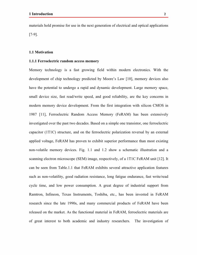
non-volatile memory devices. Fig. 1.1 and 1.2 show a schematic illustration and a
scanning electron microscope (SEM) image, respectively, of a 1T1C FeRAM unit [12]. It
can be seen from Table.1.1 that FeRAM exhibits several attractive application features
such as non-volatility, good radiation resistance, long fatigue endurance, fast write/read
cycle time, and low power consumption. A great degree of industrial support from
Ramtron, Infineon, Texas Instruments, Toshiba, etc., has been invested in FeRAM
research since the late 1990s, and many commercial products of FeRAM have been
released on the market. As the functional material in FeRAM, ferroelectric materials are
of great interest to both academic and industry researchers. The investigation of

1 Introduction 3
ferroelectric materials, including basic electrical properties and the optimization of
fabrication processes, can be valuable and directly impacts FeRAM development in the
modern memory technology field.
Fig.1.1 Schematic illustration of 1T1C and 2T2C FeRAM cell structures [12].
Fig.1.2 Scanning electron microscope (SEM) image of serial 1T1C COP FeRAM cells in a 4 Mbyte
memory, built using a 0.13μm five level Cu CMOS process [12].
1 Introduction 4
Table.1.1 Comparison of FeRAM with other existing memory technologies.
1.1.2 Ferroelectrics based microwave devices
With the development of wireless technology, electronic components working in high
frequency regions become essential to the market. Very high Q values, narrow
bandwidths, low power consumption, low insert loss, high isolation, and high operating
speeds are of great concern in such microwave components [12-14], such as resonators,
phase shifters, antennas, and tunable filters. However, in the RF-MEMS field in
particular, traditional materials such as silicon, silicon dioxide, and silicon nitride, cannot
provide efficient performance and competitive solutions due to the intrinsic nature of the
materials, and new candidate materials are in demand in the microwave electronics field.
Recently, ferroelectric materials with ultra high dielectric constants, well-defined
piezoelectric properties, and good magnetic performance, have been introduced into RF-
MEMS related research. Many filters, resonators, and delays lines, used for the resonance
of bulk or surface acoustic waves (BAWs or SAWs) are produced using ferroelectric
materials such as LiTaO3, and enhanced performance is demonstrated in such microwave
related applications [8,12]. A ferroelectric-based resonator and a ferroelectric back-to-
back resonator filler are shown in Fig.1.3 and Fig.1.4, respectively [15,16].

1 Introduction 5
Fig.1.3 Schematic illustration of an yttrium iron garnet (YIG) and ferroelectric barium strontium
titanate (BST) resonator [15].
Fig.1.4 Schematic configuration of the 3-pole back-to-back ferroelectric resonator filter [16].
Another interesting application of ferroelectrics in the microwave field is the
ferroelectric-based varactor. As a component that is of similar importance as transistors,
varactors are also widely used in microwave technologies for the purpose of analog
tuning. In order to match the application development with market demand, the III-V
semiconductor companies have put great effort into advancing existing CMOS and

1 Introduction 6
bipolar junction transistor (BJT) technologies and have succeeded in producing
commercial standard transistors with maximum oscillation frequencies above 100 GHz
[8,12,17]. However, compared to developments achieved with transistors, no
semiconductor-based varactor can provide a high enough Q factor even for frequencies
above 10-20 GHz. In a typical semiconductor varactor, the Q value decreases
proportionally with an increase in operational frequency, and falls below 10 when
operated at 50 GHz; this effectively blocks any further development of this component in
microwave electronics technology.
Reported in recent studies, the ferroelectric varactor may be employed to fulfill the need
for a high Q factor component over this frequency gap. By using tunable permittivity
ferroelectrics, it will be possible to make ferroelectric varactors with reasonable
performance at frequencies above 10-20 GHz [8,17]. With larger Q factors, high tuning
speeds, and low power consumption, the ferroelectric varactor and tunable devices have
been proven to be a feasible solution for the high frequency microwave application, and
can be well integrated with the standard silicon and GaAs fabrication processes.
Moreover, due to the intrinsic high dielectric permittivity in ferroelectrics, the size of the
ferroelectric varactor can be reduced significantly compared with CMOS technology,
which provides extra freedom and flexibility for scaling down. A schematic illustration of
a ferroelectric varactor and a typical varactor Q factor dependence on frequency are
shown in Fig.1.5 and Fig.1.6, respectively [12].

1 Introduction 7
Fig.1.5 Schematic illustration of parallel-plate and coplanar-plate ferroelectric varactor [12].
Fig.1.6 Q factor dependence on operational frequency [12].
1.1.3 Ferroelectric based optical applications
Optical applications are another important field in which ferroelectric materials can be
used. Over the last few decades, ferroelectric materials such as PZT and PLZT have been
extensively applied and investigated in photoelectron fields [18,19]. With remarkable
optoelectronic properties, high optical transparency, a large electro-optic coefficient (10-
20 times that of the traditional LiNbO3 material), good thermal stability, and fast

1 Introduction 8
switching response, ferroelectric materials have been considered a promising candidate in
the optical domain. In ferroelectric thin film based optical devices, the superior optical
properties of the ferroelectric material, along with the design flexibility of thin film
technology, offer more freedom in active optical applications and provide a number of
innovative optical devices such as micro-actuators, waveguide devices, optical memories,
optical phase retarders, optical and electro-optic switches, spatial light modulators, and
devices based on optical phase conjugation [20]. Ferroelectric optical MEMS and
ferroelectric-based E-O devices are two important application groups in the optical field,
and the large piezoelectric coefficient and large E-O coefficient of ferroelectric materials
provide a remarkable performance enhancement over traditional technologies.
1.1.4 Photovoltaic effect in ferroelectrics
Since the first report in Science 2009, the photovoltaic effect has been discovered and
studied in ferroelectric BFO [21]. The obvious photovoltaic performance improvement in
ferroelectric materials compared with traditional semiconductor p–n junctions is that the
magnitude of the built-in electrical field that separates the photo generated carriers in the
BFO crystal is nearly one order of magnitude higher than in a p–n junction. A higher
band gap photo voltage and a significant photocurrent are reported by using single crystal
BFO material of varying thickness and domain types [22,23]. As explained by the authors,
such improved photovoltaic behaviour can be attributed to the domain walls of the
ferroelectric material [22]. Another interesting phenomenon regarding this photovoltaic
effect is that the output photo voltage can be tunable in ferroelectrics. Since ferroelectric
domain structures can easily be modulated using an external electric field, by introducing
1 Introduction 9
an external electric field higher than the ferroelectric coercive field, the photovoltaic
voltage could be switched on and off, as well as flipped in polarity, after the manipulation
of ferroelectric domain structures [24]. Additionally, due to the multiferroic nature of
BFO, more control mechanics such as electricity, magnetism, heat, and stress, can be
employed to determine the photovoltaic performance of the BFO material and can
therefore be used to provide solar cells with novel functionalities [25].
1.2 Problem statement
1.2.1 Ferroelectric material: Selection and optimization
The family of ferroelectric materials has many group members. The first discovered
ferroelectric material was Rochelle Salt [2]. In 1945, ferroelectric behaviour was reported
in BaTiO3 [26]. Since then, a number of ferroelectric materials such as lead titanate
(PbTiO3), strontium bismuth tantalite (SBT), lead zirconate titanate (PZT), and lead
lanthanum zirconate titanate (PLZT), have been discovered. Among all ferroelectric
materials, the PZT material has been exploited extensively for various electrical [27-29]
and optical [30-32] applications, due to its high remanent polarization value, high optical
transmission, and strong electro-optic Kerr effect. However, PZT thin films are known to
exhibit low fatigue endurance, especially when platinum is used as electrodes. As
indicated by X. Du et al. [33], PZT thin films exhibit greater than 50% fatigue
degradation after 109 switching cycles in fatigue resistance measurements.
Recently, Nd-doped Bismuth Titanate B3.15Nd0.85Ti3O12 (BNdT) was reported by Chon
et al. [34] with a significantly larger remanent polarization (2Pr=103 μC/cm2) compared
to PZT. This surprisingly large remanent polarization can be attributed to the
1 Introduction 10
development of the polarization vector along the c-axis in the BNdT unit cell. Also, low
fatigue degradation was observed in BNdT after 1010 switching cycles, indicating
superior fatigue endurance versus PZT. There have been some studies based on the
fabrication process and ferroelectric properties characterization of the BNdT material.
However, a performance optimization process including an examination of different
fabrication parameters and elemental constituent dependence of BNdT ferroelectric
properties were not fully investigated, and research on this topic will provide a better
understanding of the nature of the BNdT ferroelectric. This work will thus help to employ
BNdT materials in more ferroelectric-based electrical applications.
1.2.2 Optical properties of ferroelectric materials
Since first being reported on by Chon et al. [34], there have been a number of papers
published that discuss the electrical properties of the BNdT ferroelectric material,
confirming the advantages of using this material in electrical related applications [35-37].
However, so far little attention has been paid to the optical properties of the BNdT
material. There was one study regarding the band gap energy fitting from an ellipsometer
measurement [38], which provided a basic theoretical understanding of the optical
properties of BNdT material. However, a detail optical investigation including parameters
such as transmittance T, refractive index n, extinction coefficient k, etc., was not
performed in its entirety. To the best of our knowledge, there has been no systematic
investigation of the optical properties of the BNdT material. Furthermore, different
impact mechanisms such as the crystallization temperature, quantum scale, and ingredient
substitution, of the BNdT thin film optical properties are never reported. Research on the
1 Introduction 11
optical properties of BNdT and its optimization process will offer a useful understanding
of the correlation between the structure and the optical properties of the material, and
thus provide more information for the future optical applications of the BNdT material.
1.2.3 Ferroelectric properties enhancement
Recently, BiFeO3 (BFO) has been recognized as a promising room temperature
multiferroic material that exhibits a ferroelectric phase transition and an anti-
ferromagnetic phase transition simultaneously [39]. Such room temperature multiferroic
behaviour offers BFO more flexibility in electrical and magnetic related applications.
However, the polarization properties of the BFO materials are only examined at low
temperature [39], due to the low electric resistivity of the BFO material at room
temperature; this is considered an obstacle which blocks the further application of the
BFO material at room temperature. The relatively low electric resistivity of BFO may be
attributed to the valence fluctuation of Fe ions (Fe2+ and F3+), which requires oxygen
vacancies for charge compensation and produces electron hopping in films. In order to
improve the polarization properties of BFO at room temperature, the site-engineering
concept has been proposed. Bi-site substitution with La and Nd atoms for controlling
volatile Bi atoms and suppressing oxygen vacancies generation has been attempted in
BFO thin films [40,41]. Meanwhile, Fe-sited substitution using Nb or Mn atoms have
been reported by S. K. Singh and C.F. Chung et al. [42,43] to fill oxygen vacancies in
bulk ceramics. However, un-doped BFO thin films still provide poor remnant polarization
at room temperature, and research in improving the room temperature ferroelectric
properties of pure BFO is necessary and will prove valuable to the ferroelectric research.
1 Introduction 12
1.2.4 Ferroelectric photovoltaic effect and its principles
Since the first report in late 2009, there have been a few studies on the photovoltaic effect
of the BFO material. Among the published works, T. Choi et al. [21] first reported the
photovoltaic effect and a direction of bulk electric polarization induced diode behaviour
in a single domain BFO crystal; S. Y. Yang et al. [22] demonstrated the electrical field
control over the domain structure in a BFO crystal and revealed the nature of the high
photovoltaic voltage in the BFO material; W. Ji et al. [44] studied the epitaxial BFO
crystal by sputtering deposition and examined photovoltaic performance dependence on
polarization. However, most of the research has focused on the single crystalline BFO
and little work has been done towards investigating the polycrystalline BFO. To the best
of our knowledge, there is only one report by B. Chen et al. [45] that presents the effect
of the top electrode (ITO and Au) on the photovoltaic response of the polycrystalline
BFO, with work that endeavors to investigate the photovoltaic properties in the sol-gel
derived BFO crystal. In fact, though single crystalline BFO derived by epitaxy
technology can exhibit well-defined photovoltaic properties, the single crystalline
fabrication process is very complicated and costly, and cannot be widely applied in large-
scale productions. The polycrystalline BFO fabricated using the sol-gel method has been
proven to be an effective and feasible candidate in commercial ferroelectric devices, and
research on the polycrystalline BFO photovoltaic effect can be an interesting topic from
the commercial perspective. Meanwhile, most of the existing photovoltaic studies are
focused on the experimental aspect, with few theoretical models having been proposed
for depicting the carriers’ transportation behaviour during the ferroelectric photovoltaic
process. Attaining and investigating the theoretical model can be an important milestone

1 Introduction 13
in understanding the photovoltaic behaviour of the BFO material and can provide us with
more theoretical support in further BFO photovoltaic applications. Moreover, all of the
work has used indium tin oxide (ITO) or metal (Au or Pt) as top electrodes, and searching
for an alternative transparent electrode and investigating the transparent enhancement to
the photovoltaic performance is always a key goal in photovoltaic research [23,45,46].
1.3 Research objective
The work conducted in this thesis aims to provide a systemic investigation of
ferroelectric materials and their electrical and optical applications. Both experimental and
theoretical examinations will be presented in detail. Broadly speaking, our research can
be divided into three phases. First, we start with fabrication of the ferroelectric material,
demonstrating a comprehensive ferroelectric parameter characterization and optimization.
Second, with the optimized ferroelectric performance, we further our research into the
optical investigation of the ferroelectric material, experimentally and theoretically, and
supplement the latter with a deeper understanding of ferroelectric optical parameters for
the first time. In the third phase, we advance our research into an innovative field of
ferroelectric research, which arose in late 2009, namely, the photovoltaic effect and its
applications; and fill some gaps existing in the development of ferroelectric photovoltaic
research.
1.4 Original contribution
As will be presented in the forthcoming chapters, our study provides novel contributions
to the field of ferroelectrics research; none of this work has been previously demonstrated.

1 Introduction 14
Evidence of the originality of our work is manifested through a series of peer-reviewed
publications based on our research, which can be found listed in the Associated
Publications Section of this thesis.
More specifically, the original contributions involved with each chapter are highlighted
and listed as follows.
Chapter 3: Ferroelectric Properties and Optimization
·Investigate and optimize the fabrication method of the BNdT ferroelectric material.
·Explore the BNdT ferroelectric properties dependence on different fabrication
parameters and elemental constituents.
Chapter 4: Optical Properties of Ferroelectrics and their Optimization
·Conduct a comprehensive optical investigation of the BNdT ferroelectric material.
·Present an experimental and theoretical investigation of the ferroelectric optical
parameters dependence on fabrication parameters.
Chapter 5: Multiferroic and Optimization
·Establish and characterize a BFO/BNdT multilayer ferroelectric structure.
·Succeed in measuring the room temperature ferroelectric remnant polarization of
pure BFO using the BFO/BNdT multilayer structure.
Chapter 6: Ferroelectric: Photovoltaic Effect and Theoretical Modeling
·Report the first photovoltaic enhancement of polycrystalline BFO ferroelectrics in a
graphene/BFO heterojunction.
·Establish the first ferroelectric photovoltaic theoretical model and explain the
carriers transportation behaviour.
1 Introduction 15
Chapter 7: Photovoltaic Performance Enhancement and Application
·Investigate the first chemical and physical enhancements of the BFO photovoltaic
performance, experimentally and theoretically.
·Implement the first optical application using the BFO photovoltaic effect.
Associated publications
The evidence of the original contributions to the overall existing body of the thesis is
manifested by the 6 peer-reviewed journal articles, as follows.
[1] Y. Y. Zang, D. Xie, Y. Chen, X. Wu, T. L. Ren, H. W. Zhu, J. L. Cao, and D. V. Plant,
“Investigation of the Improved Performance in a Graphene/polycrystalline BiFeO3/Pt
Photovoltaic Heterojunction: Experiment, Modeling, and Application,” J. Appl. Phys.,
(Under minor revision)
[2] Y. Y. Zang, D. Xie, Y. Chen, X. Wu, T. L. Ren, J. Q. Wei, H. W. Zhu, and D. V. Plant,
“Electrical and Thermal Properties of a Carbon Nanotube/Polycrystalline BiFeO3/Pt
Photovoltaic Heterojunction with CdSe Quantum Dots Sensitization,” Nanoscale, vol. 4,
pp. 2926-2930, 2012.
[3] Y. Y. Zang, D. Xie, Y. Chen, M. H. Li, C. Chen, T. L. Ren, and D. V. Plant,
“Temperature dependence of optical and structural properties of ferroelectric
B3.15Nd0.85Ti3O12 thin film derived by sol–gel process,” J. Sol-Gel Sci. Technol., vol.
61, no. 1, pp. 236-242, 2012.
[4] Y. Y. Zang, D. Xie, Y. Chen, M. H. Li, X. G. Han, T. L. Ren, and D. V. Plant,
“Comparative Study on Structural and Ferroelectric Properties of Dual-Site Rare-Earth
ions Substituted Multiferroelectric BiFeO3,” Integr. Ferroelectr., vol. 132, no. 1, pp. 30-

1 Introduction 16
38, 2012.
[5] Y. Y. Zang, D. Xie, Y. Chen, X. Wu, G. Li, and D. V. Plant, “Tuning the Structural and
Optical Properties of Bismuth Titanate by Different Nd Substitution Content,” Integr.
Ferroelectr., vol. 133, no. 1, pp. 73-80, 2012.
[6] Y. Y. Zang, D. Xie, X. Wu, Y. Chen, Y. X. Lin, M. H. Li, H. Tian, X. Li, Z. Li, H. W.
Zhu, T. L. Ren, and D. V. Plant, “Enhanced photovoltaic properties in
graphene/polycrystalline BiFeO3/Pt heterojunction structure,” Appl. Phys. Lett., vol. 99,
no. 13, pp. 132904 (3 pages), 2011.
1.5 Thesis overview
Following this introductory chapter, the organization of the remainder of the thesis is as
follows.
Chapter 2 provides the current state of the art in ferroelectric material research. We start
with an introduction to ferroelectric properties, including ferroelectric mechanisms,
fabrication methodologies, and ferroelectric performance characterization. Then,
ferroelectric-based electrical applications such as Ferroelectric Random Access Memory
(FeRAM) and the Ferroelectric Field Effect Transistor (FeFET) are briefly introduced.
We discuss current optical applications based on ferroelectric materials, such as
ferroelectric optical MEMS and ferroelectric-based EO devices. Finally, the ferroelectric
photovoltaic effect and its current research progress are presented.
In Chapter 3, we investigate the fabrication process of the Bi4-xNdxTi3O12 (BNdT)
ferroelectric thin film, and obtain an optimized fabrication routine for further applications.
We start with a discussion of the fabrication principle, and present the fabrication process

1 Introduction 17
of the BNdT ferroelectric thin film utilized in this work. Second, we continue to analyze
the structure, and show the obvious impacts of the fabrication conditions on BNdT
microstructure properties. Third, the ferroelectric and electric properties of the BNdT thin
films are investigated, and an optimized fabrication condition is obtained based on these
studies. Finally, the effect of Nd doping concentration on the BNdT thin film
optimization process is evaluated.
Chapter 4 presents the first systemic study on the correlation between different impact
mechanisms and the optical properties of the BNdT material. We start with a theoretical
analysis and introduce three different impact mechanisms, namely crystallization
temperature, quantum scale effect, and ingredient substitution, on the optical properties of
BNdT material. Then, we independently evaluate the effect of these three impact
mechanisms on the BNdT optical properties.
In Chapter 5, we explore various attempts to optimize the ferroelectric properties of
BFO material and realize room temperature characterization of the BFO material. We
start with a multilayer methodology to study the room temperature enhancement of the
BFO ferroelectric material. Fabrication technology, structural analysis, ferroelectric
characterization, and dielectric examination are described in detail in this chapter. Then,
we move on to another optimization approach, namely, dual-site substitution technology.
We process the corresponding characterization, as well as a characterization of dual-site
substituted BFO materials, demonstrated both experimentally and theoretically.
Chapter 6 presents an investigation of the enhanced photovoltaic properties in a
graphene/BFO/Pt photovoltaic heterostructure. An equivalent electrical and thermal
model is first proposed to aid in the understanding of carriers transportation behaviour.

1 Introduction 18
We start with an introduction of a five-step fabrication process for the graphene/BFO/Pt
heterojunction, followed by basic performance characteristics of the BFO material and
graphene top electrode. Then, with band diagram construction, we establish an equivalent
electrical model and calculate the BFO photocurrent J-V curves in theory. Third, we
demonstrate a detailed photovoltaic characterization of the graphene/BFO/Pt
heterojunction, and by using the theoretical model all aspects of photovoltaic
performance are investigated experimentally and theoretically.
In Chapter 7, we further our BFO photovoltaic research on performance enhancements
and the photovoltaic application. To start, we demonstrate the HNO3 treatment and
photovoltaic enhancement of the graphene/BFO/Pt. With comparison between the
experimental result and theoretical calculation, the nature of this chemical routine is
reported. We then introduce a study on physical improvements. The quantum dots (QDs)
sensitization process is explained and examined. As a comparison, we also examine the
chemical approach and the physical routine in the enhancement of the BFO photovoltaic
effect. Finally we apply our graphene/BFO/Pt photovoltaic heterojunction to the optical
and electrical fields; and a photo detector and tunable switch are built and their behaviour
demonstrated in detail.
Finally, this thesis is summarized in Chapter 8. We conclude and reiterate the central
points report in this study, and also provide ideas on the direction of future work and
other research perspectives.

2 Review of Current State-of-the-Art Research 19
Chapter 2
Review of Current State-of-the-Art Research
2.1 Introduction
he study of ferroelectric materials and their applications has been widely
reported over the past several decades, and significant research is still being
dedicated to this now flourishing field. A number of research milestones,
such as a comprehensive ferroelectric phenomenological theory and ferroelectric-based
electrical/optical applications, have been achieved in this field. In this chapter, we will
present the background and current progress of ferroelectrics research. This literature
review will help provide a solid understanding of the principles and unique properties of
ferroelectric materials, and will serve as an important theoretical basis for the
forthcoming chapters. More specifically, in Section 2.2, we start with a brief introduction
to the ferroelectric principle, followed by a review of current work on ferroelectric
materials. Different fabrication technologies for ferroelectric materials, and a comparison
of their advantages and disadvantages are also presented in this section. Section 2.3
presents ferroelectric-based electrical applications. As typical applications, ferroelectric
random access memory (FeRAM) and ferroelectric field effect transistor (FeFET) are
described in detail. In Section 2.4, we continue our discussion with ferroelectric-based
optical applications, and present current applications of ferroelectric based optical MEMS
T

2 Review of Current State-of-the-Art Research 20
and EO devices. In Section 2.5, the photovoltaic effect of ferroelectric materials and
related ongoing research is reviewed in detail.
2.2 Ferroelectric: Principles and material research
2.2.1 Ferroelectric principles
Ferroelectric materials are defined as a type of material that can possess spontaneous
polarization in a certain temperature region with external stimulation, and the intensity
and direction of the spontaneous polarization field can be modulated by external
stimulation, typically an external applied electric field. From the definition, it can be
noted that as a unique group of materials, ferroelectrics are recognized as a kind of polar
material. They have two basic features, namely, the existence of spontaneous polarization
and the ability to switch between these spontaneous polarizations. In fact, since the
discovery of the first ferroelectric in Rochelle Salt (NaKC4H4O6·4H2O), more than 200
ferroelectric materials have been discovered and reported on [2]. Ferroelectric materials
have become a large family with applications in novel functional and electrical materials.
From the crystallographic point of view, a dielectric medium that possesses a specific
crystal structure can have ferroelectric properties and can be regarded as a ferroelectric
material. As indicated in crystallographic point groups’ theory, there are 32
crystallographic point groups in total, 10 of which are polar point groups. Only crystals
that belong to these 10 polar point groups can exhibit spontaneous polarization. All
spontaneous polarized crystals possess the common property that the state of the
spontaneous polarization varies with the environmental temperature; such polarization
dependence on temperature is defined as pyroelectricity [12]. Due to the spontaneous
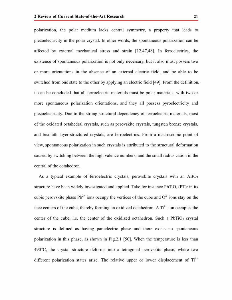
2 Review of Current State-of-the-Art Research 21
polarization, the polar medium lacks central symmetry, a property that leads to
piezoelectricity in the polar crystal. In other words, the spontaneous polarization can be
affected by external mechanical stress and strain [12,47,48]. In ferroelectrics, the
existence of spontaneous polarization is not only necessary, but it also must possess two
or more orientations in the absence of an external electric field, and be able to be
switched from one state to the other by applying an electric field [49]. From the definition,
it can be concluded that all ferroelectric materials must be polar materials, with two or
more spontaneous polarization orientations, and they all possess pyroelectricity and
piezoelectricity. Due to the strong structural dependency of ferroelectric materials, most
of the oxidated octahedral crystals, such as perovskite crystals, tungsten bronze crystals,
and bismuth layer-structured crystals, are ferroelectrics. From a macroscopic point of
view, spontaneous polarization in such crystals is attributed to the structural deformation
caused by switching between the high valence numbers, and the small radius cation in the
central of the octahedron.
As a typical example of ferroelectric crystals, perovskite crystals with an ABO3
structure have been widely investigated and applied. Take for instance PbTiO3 (PT): in its
cubic perovskite phase Pb2+ ions occupy the vertices of the cube and O2- ions stay on the
face centers of the cube, thereby forming an oxidized octahedron. A Ti4+ ion occupies the
center of the cube, i.e. the center of the oxidized octahedron. Such a PbTiO3 crystal
structure is defined as having paraelectric phase and there exists no spontaneous
polarization in this phase, as shown in Fig.2.1 [50]. When the temperature is less than
490°C, the crystal structure deforms into a tetragonal perovskite phase, where two
different polarization states arise. The relative upper or lower displacement of Ti4+
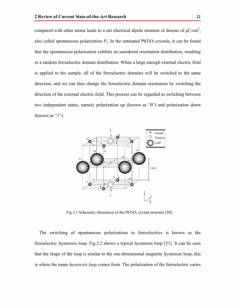
2 Review of Current State-of-the-Art Research 22
compared with other atoms leads to a net electrical dipole moment of dozens of μC/cm2,
also called spontaneous polarization Ps. In the untreated PbTiO3 crystals, it can be found
that the spontaneous polarization exhibits an unordered orientation distribution, resulting
in a random ferroelectric domain distribution. When a large enough external electric field
is applied to the sample, all of the ferroelectric domains will be switched to the same
direction, and we can thus change the ferroelectric domain orientation by switching the
direction of the external electric field. This process can be regarded as switching between
two independent states, namely polarization up (known as “0”) and polarization down
(known as “1”).
Fig.2.1 Schematic illustration of the PbTiO3 crystal structure [50].
The switching of spontaneous polarizations in ferroelectrics is known as the
ferroelectric hysteresis loop. Fig.2.2 shows a typical hysteresis loop [51]. It can be seen
that the shape of the loop is similar to the one-dimensional magnetic hysteresis loop; this
is where the name hysteresis loop comes from. The polarization of the ferroelectric varies

2 Review of Current State-of-the-Art Research 23
with the external electric field. When the electric field is large enough, the ferroelectric
polarization reaches saturation. Polarization decreases with decreasing external electric
field, but when electric field reaches zero the ferroelectric polarization is a non-zero value,
called remnant polarization (Pr). The remnant polarization is an important parameter in
ferroelectric-based applications. When the electric field reaches a certain value, the
ferroelectric polarization becomes zero; the electric field at this point is called the
coercive field (Ec). It should also be noted that the remnant polarization value is stable.
Ignoring the fatigue effect, both of these two remnant polarization states (Pr+ and Pr-) are
permanent without a large external electrical field, stress, or thermal stimulation; this is
the principle underlying the non-volatility of ferroelectric based memory devices.
Fig.2.2 Typical ferroelectric hysteresis loop [51].
Temperature is an important parameter in determining the performance of
ferroelectric materials. Ferroelectric materials can only exhibit ferroelectric properties
within a specific temperature region. When the temperature exceeds a certain value,

2 Review of Current State-of-the-Art Research 24
spontaneous polarization will disappear and the ferroelectric material will degrade into a
paraelectric [52]. This transformation temperature is called the Curie temperature (Tc).
The ferroelectric dielectric constant and permittivity will also exhibit an abnormal
tendency to vary when the temperature passes the Curie temperature. In the paraelectric
phase, the ferroelectric permittivity follows the Curie-Weiss Law as [53],
10C (T T )ε −= ⋅ − (
where
2.1)
ε is the low frequency ferroelectric permittivity, C is Curie constant of the material,
and T0 is the Curie-Weiss temperature. In second-order phase transition ferroelectrics
where the ferroelectric polarization exhibits a continuous variation, T0=Tc. In first-order
phase transition ferroelectrics where the ferroelectric polarization jumps with an increase
or decrease in temperature, T0<Tc。Such a dielectric anomaly leads to a large dielectric
constant in most ferroelectric materials. Fig 2.3 shows the dielectric constant and
spontaneous polarization variation pattern of the PbTiO3 ferroelectric [54]. In fact, the
ferroelectric dielectric constant exhibits correlation with many factors besides
temperature, such as applied voltage, chemical constituent, grain size, crystal axis, etc
[55]. For example, Ba1-xSrxTiO3 exhibits a dielectric peak when x=0.3 and BaTiO3 (BT)
shows the largest dielectric constant when the grain size is between 0.7 to 1.0 μm. Further,
in the tetragonal BaTiO3 crystal, along the c-axis the dielectric constant is 400 whereas
perpendicular to c-axis the dielectric constant is 4000 [56].
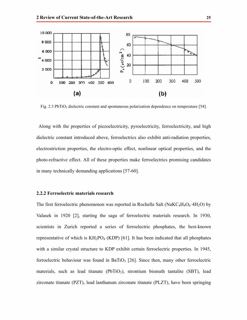
2 Review of Current State-of-the-Art Research 25
Fig. 2.3 PbTiO3 dielectric constant and spontaneous polarization dependence on temperature [54].
Along with the properties of piezoelectricity, pyroelectricity, ferroelectricity, and high
dielectric constant introduced above, ferroelectrics also exhibit anti-radiation properties,
electrostriction properties, the electro-optic effect, nonlinear optical properties, and the
photo-refractive effect. All of these properties make ferroelectrics promising candidates
in many technically demanding applications [57-60].
2.2.2 Ferroelectric materials research
The first ferroelectric phenomenon was reported in Rochelle Salt (NaKC4H4O6·4H2O) by
Valasek in 1920 [2], starting the saga of ferroelectric materials research. In 1930,
scientists in Zurich reported a series of ferroelectric phosphates, the best-known
representative of which is KH2PO4 (KDP) [61]. It has been indicated that all phosphates
with a similar crystal structure to KDP exhibit certain ferroelectric properties. In 1945,
ferroelectric behaviour was found in BaTiO3 [26]. Since then, many other ferroelectric
materials, such as lead titanate (PbTiO3), strontium bismuth tantalite (SBT), lead
zirconate titanate (PZT), lead lanthanum zirconate titanate (PLZT), have been springing
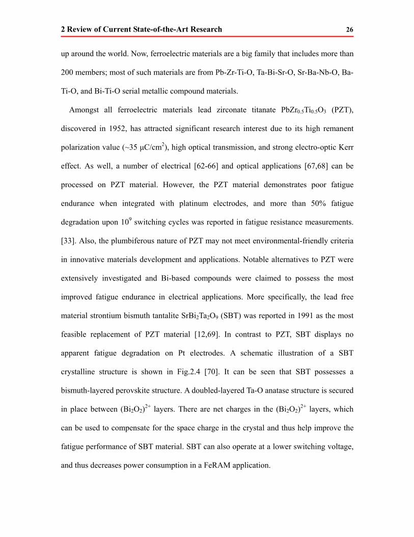
2 Review of Current State-of-the-Art Research 26
up around the world. Now, ferroelectric materials are a big family that includes more than
200 members; most of such materials are from Pb-Zr-Ti-O, Ta-Bi-Sr-O, Sr-Ba-Nb-O, Ba-
Ti-O, and Bi-Ti-O serial metallic compound materials.
Amongst all ferroelectric materials lead zirconate titanate PbZr0.5Ti0.5O3 (PZT),
discovered in 1952, has attracted significant research interest due to its high remanent
polarization value (~35 μC/cm2), high optical transmission, and strong electro-optic Kerr
effect. As well, a number of electrical [62-66] and optical applications [67,68] can be
processed on PZT material. However, the PZT material demonstrates poor fatigue
endurance when integrated with platinum electrodes, and more than 50% fatigue
degradation upon 109 switching cycles was reported in fatigue resistance measurements.
[33]. Also, the plumbiferous nature of PZT may not meet environmental-friendly criteria
in innovative materials development and applications. Notable alternatives to PZT were
extensively investigated and Bi-based compounds were claimed to possess the most
improved fatigue endurance in electrical applications. More specifically, the lead free
material strontium bismuth tantalite SrBi2Ta2O9 (SBT) was reported in 1991 as the most
feasible replacement of PZT material [12,69]. In contrast to PZT, SBT displays no
apparent fatigue degradation on Pt electrodes. A schematic illustration of a SBT
crystalline structure is shown in Fig.2.4 [70]. It can be seen that SBT possesses a
bismuth-layered perovskite structure. A doubled-layered Ta-O anatase structure is secured
in place between (Bi2O2)2+ layers. There are net charges in the (Bi2O2)2+ layers, which
can be used to compensate for the space charge in the crystal and thus help improve the
fatigue performance of SBT material. SBT can also operate at a lower switching voltage,
and thus decreases power consumption in a FeRAM application.

2 Review of Current State-of-the-Art Research 27
Fig.2.4 Schematic illustration of the SBT crystal structure [70].
However, the switchable polarization charge of SBT is much lower than for the
traditional PZT material. Another disadvantage of SBT, which may constrain its further
application, is the processing and fabrication concerns. The crystallization temperature of
SBT is significantly higher (150°C -200°C) than that of PZT. Though it is not a big issue
in laboratory research, with the increase of device density, especially under integration
with standard CMOS transistors, high process temperatures will lead to a compatibility
issue in electrical and optical applications [71]. Therefore, the search for an ideal
ferroelectric material is still of great importance in research circles today and work is
continually being performed in this field.
In 1999, B. H. Park et al. [72] reported an innovative ferroelectric material made by
replacing part of the Bi+ ions in the traditional Bi4Ti3O12 (BTO) crystal with La+ ions;
they named this new ferroelectric BLT (Bi4-xLaxTi3O12), as shown in Fig.2.5 [73].
Experiments have shown that when x=0.75, the BLT compound demonstrates the largest

2 Review of Current State-of-the-Art Research 28
remnant polarization. BLT also exhibits well-defined fatigue endurance, and little fatigue
deformation can be found upon 3×10¹⁰ switching cycles. Thereafter, lanthanide ions (La,
Sm) substituted BTO ferroelectric materials have been widely studied and reported.
Unfortunately, BLT materials are always derived using pulsed laser deposition (PLD),
which is expensive in large-scale production and can only be used in laboratory studies.
Fig.2.5 Schematic illustration of the BLT crystal structure [73].
In 2002, U. Chon et al. [34] reported a novel ferroelectric material BNdT (Bi4-
xNdxTi3O12) with remarkable ferroelectric properties, created by replacing some Bi+ ions
in the BTO with Nd+ ions. In the highly c-axis orientated BNdT, the remnant polarization
(2Pr) can reach 103 μC/cm2, compared with that of 30 μC/cm2 in the BLT material. Also,
BNdT exhibits remarkable fatigue endurance under 6.5×10¹⁰ switching cycles. As
explained by the author, this unexpected phenomena results from orientation of the
polarization vector along the c-axis of the BNdT unit cell. The expected consequence of
the higher c-axis orientation achieved in the BNdT material is that the remnant
polarization will be higher [74].

2 Review of Current State-of-the-Art Research 29
Recently, multiferroic materials have attracted ample research interest due to their
unique ferroelectric and ferromagnetic coupling [75]. The coupling of the electric and
magnetic polarization provides an extra degree of freedom in device applications such as
data storage, spintronics, sensors, actuators, and micro-electromechanical systems
(MEMS) [76-77]. As reported by J. Wang et al. [3], multiferroic BiFeO3 (BFO), as shown
in Fig.2.6, has been considered among promising room temperature multiferroic
candidates, since it exhibits both a ferroelectric phase transition at a high Curie
temperature (TC~850°C) and an anti-ferromagnetic phase transition at a high Néel
temperature (TN~370°C), rendering it both ferroelectric and ferromagnetic
simultaneously [39,78,79]. Compared with other multiferroic materials which can only
exhibit co-existing ferroelectric and ferromagnetic phase at ultra low temperatures, BFO
can be utilized in novel memory applications at room temperature.
Fig.2.6 Schematic illustration of the BFO crystal structure [3].
However, due to an intrinsic constraint of the BFO material, it is difficult to
characterize the ferroelectric properties of the pure phase BFO at room temperature

2 Review of Current State-of-the-Art Research 30
[80,81]. The low resistivity of BFO is at the root of this phenomenon. During the
annealing process, the density of oxygen vacancies reaches a dynamic balance at high
temperatures. When the material cools down, some of the oxygen vacancies are stranded
into assembled oxygen vacancies groups, resulting in an unbalanced oxygen distribution.
Such an inequilibrium leads to a Fe atom valence variation from Fe3+ to Fe2+, resulting in
a large conductivity, and thus increasing the leakage density of the BFO material. On the
other hand, BFO also possesses low dielectric constant and resistivity; this creates some
difficulty in characterizing a saturated ferroelectric hysteresis loop at room temperature.
To reduce the conductivity of BFO and measure the room temperature BFO ferroelectric
properties, different routines such as single phase technology [82], a formation of solid
solution with other ABO3 pervoskite materials [83], and ion atoms substitution at Bi and
Fe sites in the BFO crystal [84] have been widely investigated with some promising
results having been achieved thus far.
2.2.3 Ferroelectric fabrication technology
In modern electrical and optical applications, ferroelectric materials are always used in
the form of a thin film. There are many fabrication technologies for ferroelectric thin
films, and most of the existing thin film fabrication technologies have already been
attempted on ferroelectric materials. There are four major fabrication routines used in
laboratory research and in commercial development; they are discussed in turn below.
Sputtering
In sputtering technology, a high-energy particle stream bombards the target material, and
the target atoms fall and depose onto the surface of the substrate, thereby forming the

2 Review of Current State-of-the-Art Research 31
desired material thin film, as indicated in Fig.2.7 [85]. Sputtering is a mature technology
that was used in early titanates and bismuth ferroelectric thin film preparations. It has
wide application perspectives for modern ferroelectric material thin film deposition. Due
to the high energy of the sputtering particle stream, thin films prepared by sputtering can
always exhibit a high surface mobility in electrical applications.
Fig.2.7 Schematic illustration of the sputtering technology [85].
The advantages of sputtering can be summarized as follows:
(1) The thin film achieved can exhibit a well-defined degree of crystallization, and with
appropriate fabrication parameters even single crystal thin film can be obtained;
(2) A low fabrication temperature;
(3) Good compatibility with the CMOS integration process;
(4) Flexibility in depositing various kinds of ferroelectric materials.
However, there are also some disadvantages with using sputtering technology, such as
the low deposition rate, small guaranteed chip area, and the constituent variation at
different chip locations. Recently, many optimized sputtering technologies, such as RF

2 Review of Current State-of-the-Art Research 32
sputtering, reactive sputtering, multiple targets sputtering, and ion beam sputtering, have
been widely reported in fabricating ferroelectric thin films such as BaTiO3, Bi4Ti3O12,
and SrBi2Ta2O9. FeRAM from Ramtron is also fabricated using RF sputtering technology.
Pulsed Laser Deposition (PLD)
In PLD technology, a high intensity pulsed laser beam created by an excimer laser is
focused on the surface of the target, heating and fusing the target material into a high
temperature and high pressure plasma. This plasma expands and emits in a specific
direction, and deposits on the heated substrate surface. Fig.2.8 shows a schematic
depicting the PLD technology [86]. The advantages of the PLD method can be
summarized as follows,
(1) Capable of fabricating complex constituent ferroelectric thin films;
(2) Introduces active gases such as oxygen, and can improve the crystallization quality
of most multi-oxide ferroelectric materials;
(3) Capable of depositing multilayer thin films;
(4) Provides a well-defined ferroelectric crystal structure;
(5) Can have an in-situ annealing process for the deposited thin film.
Fig.2.8 Schematic depicting of the PLD technology [86].

2 Review of Current State-of-the-Art Research 33
PLD technology was initially used in depositing TC superconductive thin films. It has
now been successfully applied to fabrication of ferroelectric thin films such as PZT,
PLZT, and BST. However, the high cost and low yield make it inappropriate for large-
scale production, and it is for this reason that the technology is currently widely used only
at the laboratory research level.
Sol-gel method
In the Sol-gel method, different metal alkoxides are dissolved into a predetermined
solvent, and react into a complex alkoxide. With the help of the solvent and catalyst,
complex alkoxide hydrolyzes or alcoholizes into solution and gelatin. A ferroelectric thin
film can then be obtained using spin coating technology, drying, and sintering. There are
two major steps that ensure the success of the sol-gel technology, namely, obtaining a
stable solution and effective control over the condensation reaction during the gelation
process. In order to obtain a stable solution, the following criteria for the metal alkoxides
solute should be met:
(1) Rich in metal content;
(2) High solubility in the solvent;
(3) No melting or evaporating during the drying and annealing processes;
(4) Stable at room temperature.
The annealing temperature and ramping rate are two important parameters in sol-gel
technology. The annealing temperature determines the final crystal structure achieved in
the ferroelectric thin film. For example, the annealing temperature can fully determine the
pyrochlore or perovskite structures in the as-prepared thin film. Meanwhile, the ramping
rate determines the stress relaxation process and thus the microstructure of the thin film.

2 Review of Current State-of-the-Art Research 34
Sol-gel technology has several advantages including low cost, high production yield, high
deposition rate, and that it is a promising fabricating method in large-scale commercial
production. On the other hand, the crystals prepared using sol-gel are always
polycrystalline, and may not compare with the materials achieved using other physical
deposition methods such as PLD and RF sputtering. Many ferroelectric materials, such as
PbTiO3, PZT, PLZT, BaTiO3, KNbO3, Bi4Ti3O12, and (Sr, Ba)NbO3, have been reportedly
fabricated using the sol-gel method.
Metal organic chemical vapor deposition (MOCVD)
In MOCVD technology, the metal organic chemical vapor is transported into the reaction
chamber, decomposed and deposited on the surface of the heated substrate. Fig.2.9 shows
a schematic illustration of the MOCVD process [87]. The vapor sources are always
hydroxyl compounds, alkoxide, and aryl compounds. The advantages of MOCVD
technology can be summarized as follows:
(1) Low substrate temperature;
(2) High growth rate;
(3) Precise control in element constituent;
(4) Large area of uniformity and consistency;
(5) Can be deposited on non-planar substrates to directly fabricate a patterned device;
(6) Suitable for large-scale commercial fabrication.

2 Review of Current State-of-the-Art Research 35
Fig.2.9 A schematic illustration of the MOCVD process [87].
There are more than ten ferroelectric materials including PZT, PbTiO3, and BaTiO3, that
can be grown using MOCVD; however, due to limited suitable source vapors, many
ferroelectric materials cannot yet be fabricated using this technology. Research and
development for innovative, low volatilization temperature, and low toxic MO sources
are still popular topics in the MOCVD field.
2.3 Ferroelectric based electrical application
In 1987, the first ferroelectric-based memory device was reported in the U.S., and
significant attention has been paid to this thriving field ever since. Many academic and
industrial institutions have invested substantial effort in the investigation and
commercialization processes of this new technology, which also accelerates the
development of ferroelectric-based electrical applications. As introduced in Chapter 1,

2 Review of Current State-of-the-Art Research 36
ferroelectric-based memory devices demonstrate remarkable application advantages over
other existing memory devices. Due to their nonvolatile nature and unique ferroelectric
related properties, ferroelectric based memory devices can not only replace existing
nonvolatile memory devices, but may also be employed in novel applications that were
unfathomable with traditional memory devices. For instance, ferroelectric based memory
devices can be used in aerospace applications because of their significant anti-radiation
resistance; and they can be employed in specific applications such as TV channel
memories, digital memories for game machines, and counters for odometers or printers,
owing to their well defined Read/Write endurance. This type of device could also be
introduced into memory units in mobiles, beepers, and Radio frequency identifications
(RFID), thanks to its natural low power consumption. Moreover the device’s re-
programmability, low power consumption and long lasting properties make it a promising
candidate in IC card related applications. In fact, some semiconductor companies have
already begun research on integrating ferroelectric materials into the non-contact IC card
application.
The operating principle of ferroelectric based memory devices is that the ferroelectric
thin film memory unit can be polarized into two different polarization states (Pr+ and Pr-)
by an external electric field, and these two states can be regarded as “1” and “0”,
respectively, thus effectively realizing binary storage. There are two major application
forms of ferroelectric based memory devices, namely, Ferroelectric Random Access
Memory (FeRAM) and Ferroelectric Field Effect Transistor (FeFET).

2 Review of Current State-of-the-Art Research 37
2.3.1 Ferroelectric random access memory (FeRAM)
The operating principle of FeRAM is based on the ferroelectric spontaneous polarization,
making FeRAM a kind of nonvolatile memory device. FeRAM has the fast Read/Write
feature of static random access memory (SRAM), the high integration density of dynamic
random access memory (DRAM), the nonvolatility of read only memory (ROM), and can
be widely applied to many technically demanding applications.
In general, FeRAM has three different application structures, namely 1T1C, 2T2C and
Chain structure. In the 2T2C structure, the cell circuit of FeRAM is similar to that of
DRAM. In Fig.2.10, the schematic of one 1T1C ferroelectric memory unit is shown. One
side of the ferroelectric capacitor is connected to the bit line (BL) through a MOSFET,
for which ON/OFF is controlled by a word line (WL), and the other side is connected to a
pulsed common plate (PLP) [88]. If two such memory units are operated as a pair, storing
opposite data information, they can operate as a reference for each other. By employing a
sensitive amplifier (SA) connected to the BL output, such a ferroelectric memory unit
composed of two MOSFETs and two ferroelectric capacitors is defined as a 2T2C unit, as
shown in Fig.2.11 [88]. The 2T2C unit is the most common FeRAM unit. It possesses
high reliability and low design complexity. However, the large occupied chip area in such
a structure does not meet the high-density design principle requirements. Compared with
the 2T2C unit, the 1T1C unit saves 50% of the chip area, which is beneficial to the high-
density design. However, the generation of a reference signal and the reliability of the
design involve more design and fabrication issues.

2 Review of Current State-of-the-Art Research 38
Fig.2.10 Schematic diagram of a 1T1C FeRAM unit [88].
Fig.2.11 Schematic diagram of a 2T2C FeRAM unit [88].
In the chain structure, shown in Fig.2.12 [89], multiple 1T1C FeRAM units are placed
in series, and the ferroelectric capacitors are short-circuited by MOSFETs when accessed.
Compared with the traditional memory structure, such chain structures exhibit a more
compact design and can be employed in ultra high-density circuit applications.
Fig.2.12 Schematic diagram of a FeRAM chain [89].

2 Review of Current State-of-the-Art Research 39
2.3.2 Ferroelectric field effect transistor (FeFET)
An alternative approach to ferroelectric based nonvolatile storage is the ferroelectric field
effect transistor (FeFET). Fig 2.13 (a) shows a cell diagram of a 1T FeFET cell, where a
ferroelectric layer replaces the gate oxide layer on a typical MOSFET [12]. Using a p-
type substrate, for example, the operating principle can be explained as follows. When
the gate voltage exceeds the threshold voltage, a conducting channel is established
between the source and drain. Unlike with the traditional MOSFET, an external applied
voltage polarizes the ferroelectric thin film, and when the gate voltage is removed the
conducting channel still exists due to the ferroelectric remnant polarization. The drain
current can still be measured when an external voltage is applied between the source and
drain electrodes. When a negative voltage is applied to the gate, the ferroelectric
polarization will decrease and then reverse polarization. Consequently, the conducting
channel will narrow or disappear, and the drain current will decrease correspondingly.
When the voltage is removed, a negative ferroelectric remnant polarization field will
maintain the majority carrier accumulation state, and prevent the formation of drain
current. A transfer characteristic is given in Fig 2.13 (b), and it can be seen that by
introducing a ferroelectric material as the dielectric layer, the drain current can be
significantly amplified or reduced compared with that of the traditional MOSFET, and
thus the drain current can be used to read the stored “1” or “0” information [12].

2 Review of Current State-of-the-Art Research 40
Fig.2.13 (a) Schemetic diagram of a FeFET cell. (b) A typical transfer characteristic of FeFET [12].
Although there has been significant research on FeFETs, compared with the wide
application of FeRAM there have not yet been any commercial FeFET products reported.
The major problems that constrain further application of FeFETs are the retention time
and fabrication integration issues. Unlike the FeRAM, where the ferroelectric capacitor is
approximately 100 nm apart from the MOSFET, the ferroelectric material is in direct
contact with the conducting channel of the MOSFET transistor [12]. The FeFET itself is
a single device and the ferroelectric thin film acts as the functional and active part in the
transistor. Therefore, the interface properties, such as localized states and impurities
between the ferroelectric thin film and silicon wafer, will play an important role in
determining the electrical performance of parameters including threshold voltage,
saturation voltage, C-V curves, etc., of the FeFET. In fact, research indicates that there is
considerable inter-diffusion between the ferroelectric material and silicon, especially
during the annealing process [90,91]. Such inter-diffusion, along with some charge
parasitic effects, will deteriorate the interface properties and reduce the retention time of
the FeFET [12]. Several approaches have been proposed to increase the retention time of
the FeFET; the most effective solution is to incorporate a high-K dielectric buffer layer
between the ferroelectric thin film and the silicon substrate, as shown in Fig 2.14 [12].

2 Review of Current State-of-the-Art Research 41
Such a metal-ferroelectric-insulator-silicon (MFIS) structure will significantly reduce the
diffusion around the interface and improve the retention time of the FeFET [92,93].
Many buffer layer materials, such as SiO2, Si3N4, SrTiO3, TiO2, etc., have been
investigated over the past decade [94-96], and HfO2 in particular has proven to be a
promising candidate with which the retention time of the SBT based FeFET can be
improved to more than 30 days [92,97].
Fig.2.14 Schemetic diagram of the MFIS FeFET cell [12].
Besides research on the insulating layer, there exist other approaches for improving the
current performance of the FeFET. For example, more complex gate sequences, namely,
a metal-ferroelectric-metal-insulator-silicon (MFMIS) structure has been reported, where
the optimized MFM structure from FeRAM can be employed during FeFET fabrication.
Also, such a multilayer gate can provide more flexibility in optimizing and matching the
infection charge issue between the ferroelectric thin film and the silicon substrate
[12,92,98]. Meanwhile, inspired by the refresh unit in DRAM, a FeDRAM unit, namely,
a FeFET unit with a refresh circuit is also reported as a compromise to the retention
concern in the traditional FeFET. Unlike the high refresh frequency in DRAM, the
refresh frequency in the FeDRAM can be as low as one per month, and methods to

2 Review of Current State-of-the-Art Research 42
improve the retention time of the FeFET unit can even further reduce the refresh
frequency [99,100]. Though research aimed at solving many application concerns of
FeFET is on going, development of innovative designs and fabrication optimization will
make possible the commercialization of FeFET in the near future.
2.4 Ferroelectric based optical applications
2.4.1 Ferroelectric optical MEMS
Micro-electromechanical systems (MEMS) have been extensively investigated for use in
various applications, including as integrated accelerometers for auto-sensors, micro-
mirrors for display and telecommunications, and micro-cantilevers for microscopes
[12,101-105]. In its early stages, silicon based technology was well incorporated into the
MEMS production process, which provided a remarkable contribution to the
commercialization of MEMS technology. It is for this reason that the term MEMS has
been associated with CMOS for such a long time. As an important application device,
flat micro-mirrors driven by MEMS actuators are widely used in laser scanner displays,
barcode readers, and laser printers [106,107]. Due to limited material selection, the
actuators that are used to drive the micro-mirrors are all silicon based electrostatic
actuators or electrothermal actuators [105,108]. With the development of modern MEMS
technology, especially with the increase in flat micro-mirror area, use of the traditional
electrostatic force or electrothermal force cannot meet the requirements of modern
driving forces, due to their high operation voltage, non-linear operation and pull-in
phenomenon. Electromagnetic actuators can provide a large driving force, but the large
bulk volume cannot meet the micro design criteria [101]. Innovative actuators that can
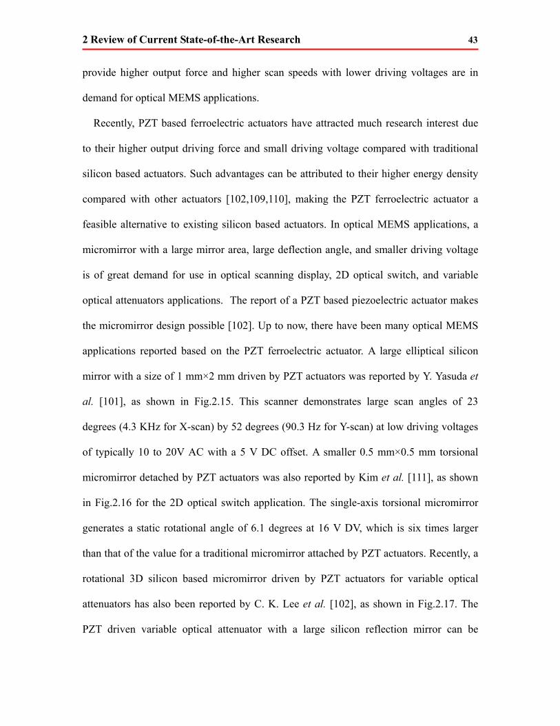
2 Review of Current State-of-the-Art Research 43
provide higher output force and higher scan speeds with lower driving voltages are in
demand for optical MEMS applications.
Recently, PZT based ferroelectric actuators have attracted much research interest due
to their higher output driving force and small driving voltage compared with traditional
silicon based actuators. Such advantages can be attributed to their higher energy density
compared with other actuators [102,109,110], making the PZT ferroelectric actuator a
feasible alternative to existing silicon based actuators. In optical MEMS applications, a
micromirror with a large mirror area, large deflection angle, and smaller driving voltage
is of great demand for use in optical scanning display, 2D optical switch, and variable
optical attenuators applications. The report of a PZT based piezoelectric actuator makes
the micromirror design possible [102]. Up to now, there have been many optical MEMS
applications reported based on the PZT ferroelectric actuator. A large elliptical silicon
mirror with a size of 1 mm×2 mm driven by PZT actuators was reported by Y. Yasuda et
al. [101], as shown in Fig.2.15. This scanner demonstrates large scan angles of 23
degrees (4.3 KHz for X-scan) by 52 degrees (90.3 Hz for Y-scan) at low driving voltages
of typically 10 to 20V AC with a 5 V DC offset. A smaller 0.5 mm×0.5 mm torsional
micromirror detached by PZT actuators was also reported by Kim et al. [111], as shown
in Fig.2.16 for the 2D optical switch application. The single-axis torsional micromirror
generates a static rotational angle of 6.1 degrees at 16 V DV, which is six times larger
than that of the value for a traditional micromirror attached by PZT actuators. Recently, a
rotational 3D silicon based micromirror driven by PZT actuators for variable optical
attenuators has also been reported by C. K. Lee et al. [102], as shown in Fig.2.17. The
PZT driven variable optical attenuator with a large silicon reflection mirror can be
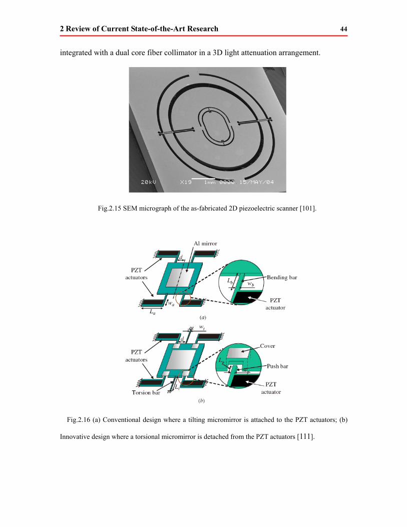
2 Review of Current State-of-the-Art Research 44
integrated with a dual core fiber collimator in a 3D light attenuation arrangement.
Fig.2.15 SEM micrograph of the as-fabricated 2D piezoelectric scanner [101].
Fig.2.16 (a) Conventional design where a tilting micromirror is attached to the PZT actuators; (b)
Innovative design where a torsional micromirror is detached from the PZT actuators [111].
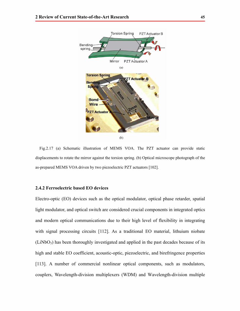
2 Review of Current State-of-the-Art Research 45
Fig.2.17 (a) Schematic illustration of MEMS VOA. The PZT actuator can provide static
displacements to rotate the mirror against the torsion spring. (b) Optical microscope photograph of the
as-prepared MEMS VOA driven by two piezoelectric PZT actuators [102].
2.4.2 Ferroelectric based EO devices
Electro-optic (EO) devices such as the optical modulator, optical phase retarder, spatial
light modulator, and optical switch are considered crucial components in integrated optics
and modern optical communications due to their high level of flexibility in integrating
with signal processing circuits [112]. As a traditional EO material, lithuium niobate
(LiNbO3) has been thoroughly investigated and applied in the past decades because of its
high and stable EO coefficient, acoustic-optic, piezoelectric, and birefringence properties
[113]. A number of commercial nonlinear optical components, such as modulators,
couplers, Wavelength-division multiplexers (WDM) and Wavelength-division multiple

2 Review of Current State-of-the-Art Research 46
access (WDMA), are produced based on lithium niobate (LiNbO3). However, recent
studies indicate that many typical ferroelectric materials, especially single crystalline
ferroelectrics, may serve as a promising replacement for traditional LiNbO3 materials
thanks to their ultra high EO coefficients. Compared with LiNbO3, whose high frequency
EO coefficient (r33) is 30.8 pm/V, single crystalline lithium titanate (LiTaO3)
demonstrates a r33 of 35.8 pm/V, the r33 value is reported to be as high as 820 pm/V in
single crystalline barium titanate (BaTiO3), and single crystalline potassium niobate
(KNbO3) exhibits a linear EO coefficient of 450 pm/V. Moreover, a solid solution of
KNbO3 and KTaO3 (KTaxNb1-xO3) has been reported with an ultra high EO coefficient of
~2000 pm/V [114,115].
Among the various ferroelectric materials, BaTiO3 and PLZT should be highlighted for
use in optical applications. The BaTiO3 material exhibits a high self pumped phase
conjugation reflection and optical two wave mixing efficiency, and has been widely
applied in the optical modulator field. As shown in Fig.2.18, an optical waveguide
modulator is built using the BaTiO3 material; the low Vπ voltage at 1550 nm wavelength
and the short electrodes (3 nm) make it a promising candidate for use in modulators [116].
Also, another study demonstrates a BaTiO3 waveguide modulator with voltage-length
products of 0.5 Vcm and an effective EO coefficient of 360 pm/V at 1561 nm, as shown
in Fig. 2.19 [117].
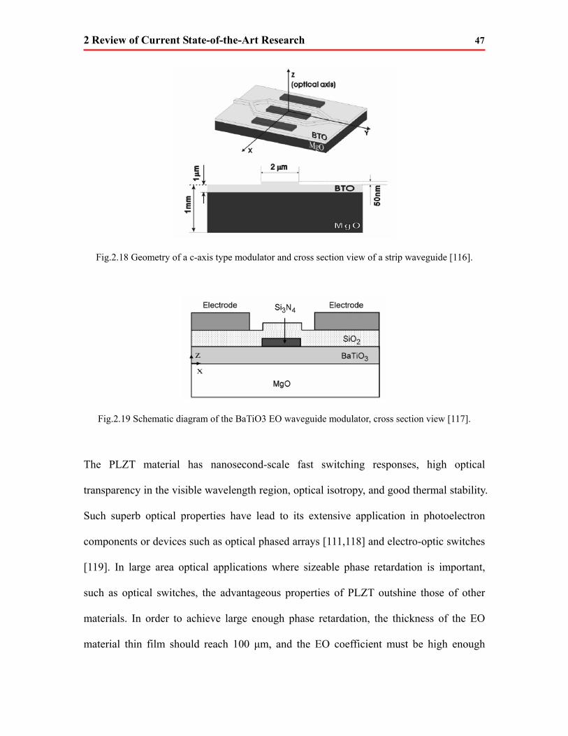
2 Review of Current State-of-the-Art Research 47
Fig.2.18 Geometry of a c-axis type modulator and cross section view of a strip waveguide [116].
Fig.2.19 Schematic diagram of the BaTiO3 EO waveguide modulator, cross section view [117].
The PLZT material has nanosecond-scale fast switching responses, high optical
transparency in the visible wavelength region, optical isotropy, and good thermal stability.
Such superb optical properties have lead to its extensive application in photoelectron
components or devices such as optical phased arrays [111,118] and electro-optic switches
[119]. In large area optical applications where sizeable phase retardation is important,
such as optical switches, the advantageous properties of PLZT outshine those of other
materials. In order to achieve large enough phase retardation, the thickness of the EO
material thin film should reach 100 μm, and the EO coefficient must be high enough

2 Review of Current State-of-the-Art Research 48
[120]. However, there are many fabrication concerns with thick film deposition, such as
film uniformity and inner stress release, which constrains the further research of such
optical applications. The employment of PLZT can somewhat reconcile the thickness
requirement and thus reduce the complexity of the device’s fabrication and integration.
Also, the high optical transparency of PLZT offers more economical benefits in the
device design and implementation. Further, the dielectric and optical properties of PLZT
can be modulated by changing the elemental constituents of the PLZT material [121].
Such changes in elemental constituents can create materials with different EO
performance and can be attractive in modern optical applications where optical parameter
matching is of importance. Fig.2.20 shows the design of a ridge type Mach-Zehnder
modulator based on a PLZT waveguide [122].
Fig.2.20 (a) A schematic diagram of the PLZT waveguide (b) Geometry of a Mach-Zehnder modulator
based on the PLZT waveguide [122].

2 Review of Current State-of-the-Art Research 49
2.5 Photovoltaic effect in ferroelectrics
In 2009, the photovoltaic effect was first reported in multiferroic BFO materials by T.
Choi et al. [21]. Since most ferroelectric materials possess relatively large band gap
energy, the small optical band gap of ~2.2 eV in bulk BFO makes its use possible in
photovoltaic applications. By using an Au electrode, the BFO single crystal bulk exhibits
a diode-like photocurrent under visible light illumination. The ferroelectric photovoltaic
effect also varies with the direction of the polarized-light electric field, as shown in
Fig.2.21. When the BFO bulk rotates under illumination with a linearly polarization light,
the photovoltaic effect reaches maximum when the polarized-light electric field and in-
plane component of the ferroelectric polarization are parallel, and it becomes minimum
when the field is perpendicular to the in-plane component.
Fig.2.21 The photovoltaic performance dependence on different polarization states of incident light
[21].
Immediately following this, in a report in Nature nanotechnology, S. Y. Yang et al.
investigated specifically patterned ferroelectric bulks with different domain types, and
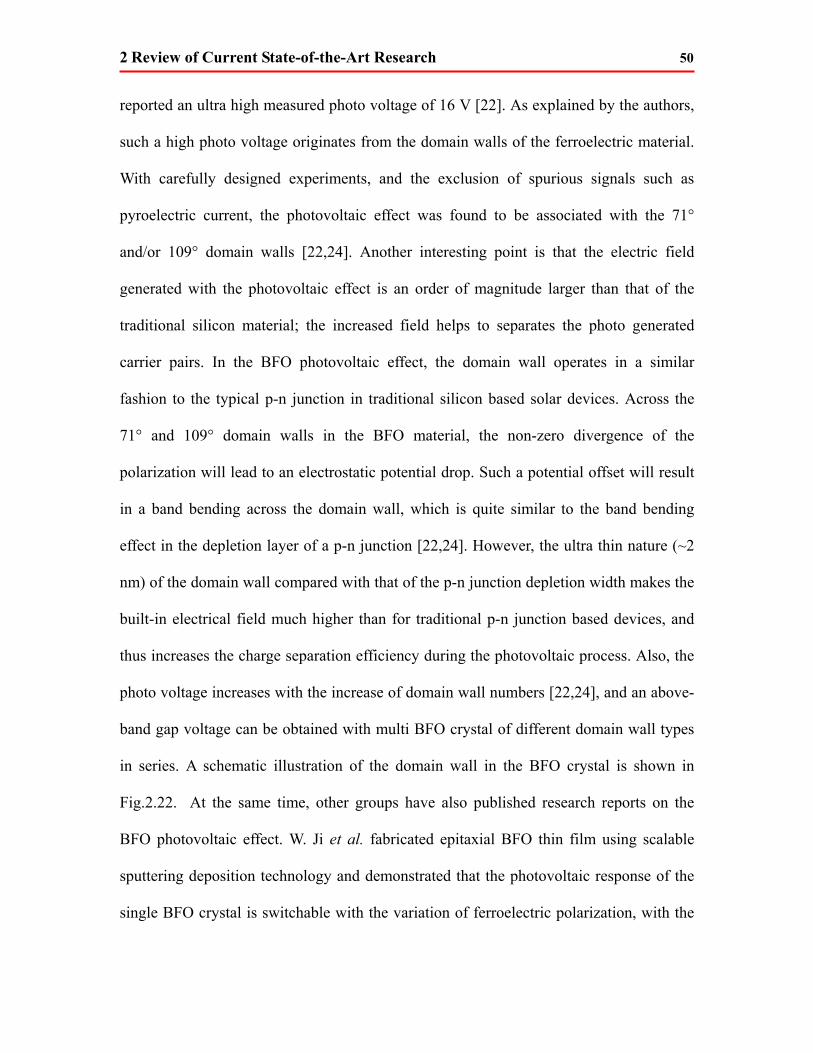
2 Review of Current State-of-the-Art Research 50
reported an ultra high measured photo voltage of 16 V [22]. As explained by the authors,
such a high photo voltage originates from the domain walls of the ferroelectric material.
With carefully designed experiments, and the exclusion of spurious signals such as
pyroelectric current, the photovoltaic effect was found to be associated with the 71°
and/or 109° domain walls [22,24]. Another interesting point is that the electric field
generated with the photovoltaic effect is an order of magnitude larger than that of the
traditional silicon material; the increased field helps to separates the photo generated
carrier pairs. In the BFO photovoltaic effect, the domain wall operates in a similar
fashion to the typical p-n junction in traditional silicon based solar devices. Across the
71° and 109° domain walls in the BFO material, the non-zero divergence of the
polarization will lead to an electrostatic potential drop. Such a potential offset will result
in a band bending across the domain wall, which is quite similar to the band bending
effect in the depletion layer of a p-n junction [22,24]. However, the ultra thin nature (~2
nm) of the domain wall compared with that of the p-n junction depletion width makes the
built-in electrical field much higher than for traditional p-n junction based devices, and
thus increases the charge separation efficiency during the photovoltaic process. Also, the
photo voltage increases with the increase of domain wall numbers [22,24], and an above-
band gap voltage can be obtained with multi BFO crystal of different domain wall types
in series. A schematic illustration of the domain wall in the BFO crystal is shown in
Fig.2.22. At the same time, other groups have also published research reports on the
BFO photovoltaic effect. W. Ji et al. fabricated epitaxial BFO thin film using scalable
sputtering deposition technology and demonstrated that the photovoltaic response of the
single BFO crystal is switchable with the variation of ferroelectric polarization, with the
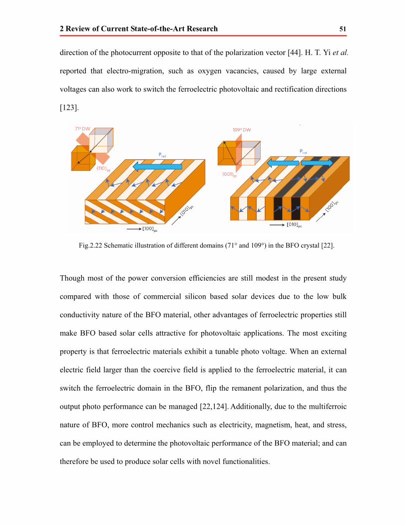
2 Review of Current State-of-the-Art Research 51
direction of the photocurrent opposite to that of the polarization vector [44]. H. T. Yi et al.
reported that electro-migration, such as oxygen vacancies, caused by large external
voltages can also work to switch the ferroelectric photovoltaic and rectification directions
[123].
Fig.2.22 Schematic illustration of different domains (71° and 109°) in the BFO crystal [22].
Though most of the power conversion efficiencies are still modest in the present study
compared with those of commercial silicon based solar devices due to the low bulk
conductivity nature of the BFO material, other advantages of ferroelectric properties still
make BFO based solar cells attractive for photovoltaic applications. The most exciting
property is that ferroelectric materials exhibit a tunable photo voltage. When an external
electric field larger than the coercive field is applied to the ferroelectric material, it can
switch the ferroelectric domain in the BFO, flip the remanent polarization, and thus the
output photo performance can be managed [22,124]. Additionally, due to the multiferroic
nature of BFO, more control mechanics such as electricity, magnetism, heat, and stress,
can be employed to determine the photovoltaic performance of the BFO material; and can
therefore be used to produce solar cells with novel functionalities.

2 Review of Current State-of-the-Art Research 52

3 Ferroelectric Properties and Optimization 53
Chapter 3
Ferroelectric Properties and Optimization
3.1 Introduction
he fabrication process and ferroelectric characterization are a fundamental
part of all research related to ferroelectric materials. The investigation of an
optimized fabrication process for ferroelectric materials is crucial in our
work and is the basis of the optical and photovoltaic research in the coming chapters. In
this chapter, we investigate the fabrication process of the Bi4-xNdxTi3O12 (BNdT)
ferroelectric thin film, and obtain an optimized fabrication process routine for further
applications. More specifically, Section 3.2 discusses the principle behind the sol-gel/spin
coating process, describes the precursor preparation process for the BNdT ferroelectric
solution, and illustrates the fabrication process of the BNdT ferroelectric thin film
achieved in this work. Section 3.3 starts with the structural analysis, and shows the
obvious impacts of the fabrication conditions on the BNdT XRD, SEM, AFM, TEM, etc.
microstructure properties. Next, in Section 3.4, the ferroelectric and electric properties of
the BNdT thin films are investigated, and an optimized fabrication condition is obtained
based on these studies. In Section 3.5, the Nd doping concentration, as a different point of
T

3 Ferroelectric Properties and Optimization 54
view, is evaluated in the BNdT thin film optimization process. Finally, this chapter is
summarized and concluded in Section 3.6.
3.2 Fabrication and optimization
The fabrication technology of ferroelectric materials involves all of the traditional
semiconductor fabrication technologies, such as solution-gelatin (sol-gel), chemical vapor
deposition (CVD), radio-frequency sputtering (RF sputtering), metal organic chemical
vapor deposition (MOCVD), pulsed laser deposition (PLD), and molecular beam epitaxy
(MBE), etc. Physical fabrication approaches, such as PLD, RF sputtering, and MBE, can
provide a better ferroelectric phase orientation and precise control over the elemental
constituents that make up the compounds; thus enabling better ferroelectric properties in
applications. However, the high cost and low growth rate constrain their application in
large-scale fabrications. Chemical routines, on the other hand, including sol-gel, CVD,
and MOVCD, demonstrate a large fabrication efficiency and low facility cost, and have
been widely utilized in many commercial ferroelectric industries.
In this study, the sol-gel/spin coating method is chosen as the principle fabrication
method for the BNdT ferroelectric material. The low operation temperature and high
uniformity and consistency make it a promising method in optical related applications.
3.2.1 Sol-gel technology
Sol-gel technology: Theory
The sol-gel method is a typical wet chemical route, with the starting material (precursor)
being prepared with either inorganic salt or metal alkoxide. The principle reaction routine

3 Ferroelectric Properties and Optimization 55
can be classified through three steps. First, the precursor dissolves in water or an organic
solvent until becoming a uniform and stable solution. Second, the precursor hydrolyzes or
alcoholize, and the product assembles in particles with 1 nm in diameter, thereby creating
the solution. Finally, the solution evaporates and turns into gelatin. This process can be
explained through the following equations [125].
(1) Solvation: M(H2O)nz+——M(H2O)n-1(OH)(z-1)++H+
The metal cation Mz+ in the salt ionizes and combines with a water molecule, resulting
in the solvent unit M(H2O)z+. Many H+ have been released in this process to maintain the
ligancy of the metal cation. If other cations exist, a complex polyreaction can occur at
this time.
(2) Hydrolyzation: M(OR)n+XH2O——M(OH)X(OR)n-X+XROH
The unionized molecule precursor, such as metal alkoxide M(OR)n, hydrolyzes and
produces M(OH)n.
(3) Condensation, which includes:
Dehydration condensation: M-OH+HO-M——M-O-M+H2O
Loss of alcohol condensation: MOR+HO-M——M-O-M+ROH
The reaction products are colloidal particles with different structures and sizes.
Sol-gel technology: Fabrication process
The sol-gel fabrication process can be described in three steps, as illustrated in Fig.3.1

3 Ferroelectric Properties and Optimization 56
Fig 3.1 Fabrication flowchart of sol-gel technology.
First, dissolve the metal alkoxide in solvent. Since the solubility of the metal alkoxide
in the water is limited, alcohol is always introduced to aide the dissolution process.
Catalysts such as HCl and NH4OH will also be added to this process to modulate the rate
of hydrolysis and condensation. In order to ensure the uniformity and homogeneity of the
precursor, stirring is both necessary and indispensable throughout this process. The
second step is to prepare the solution. There are two major routines during the solution
preparation process, namely, solution polymerization and the particle method. The core
difference between these two methods is the amount of solvent added to the system. In
the solution polymerization, little solvent is introduced, and hydrolysate can continue to
react with the non-hydrolyzed metal alkoxide. However, the particle method ensures the
reaction occurs under completed hydrolyzation of the metal alkoxide, and therefore
adequate solvent should be provided. Since the hydrolyzation and condensation play an

3 Ferroelectric Properties and Optimization 57
important role in the solation reaction, reaction parameters such as the solvent load,
catalyst, and pH of the solution, should be well managed in this process. Third, age the
solution into the wet gelatin. When the as-prepared solution is left to stand in an open or
closed container, the existing particles in the solution will exhibit a “survival growth”,
namely, particles with larger size will expand while smaller particles will further shrink.
This process is named Ostwald ripening [125], as illustrated in Fig.3.2. During the aging
process, the solution particles connect into a network structure, and the fluidness of the
entire system decreases, changing the solution system from a Newtonian fluid to
Bingham plastic [125-127]. The forming processes such as fibrosis, spin coating, and
casting can be implemented during this step. Fourth, dry the gelatin. There is a large
amount of solvent or water in the wet gelatin, and the volume of the system shrinks
significantly during the drying process, increasing the possibility of deformation and
cracking. Therefore, the prevention of deforming and cracking is a key technology during
the sol-gel/spin coating process, especially for large bulk substrates. Precise control over
the drying conditions, addition of chemical additives, and supercritical drying, are some
of the commonly used technologies in the current sol-gel fabrication field. Finally, anneal
the as-prepared dry gelatin. The purpose of this step is to minimize the remaining air and
solvent in the gelatin, increase the gelatin density, and help to achieve the desired
crystalline phase. Due to the high specific surface area and high activity of the gelatin,
the annealing temperature is much lower compared with that of ceramic sintering. Hot
pressed sintering is always introduced as a popular technology to reduce the sintering
time and increasing sintering quality [127,128].

3 Ferroelectric Properties and Optimization 58
Fig 3.2 Schematic illustration of Ostwald ripening.
3.2.2 Precursor preparation
In this study, the molecular formula of the BNdT sample is Bi4-xNdxTi3O12 (x=0.85),
namely, Bi3.15Nd0.85Ti3O12. To obtain the desired element ratio in the BNdT thin film, the
appropriate metal salt solute and corresponding solvent should be employed to provide a
stable and uniform solution.
According to the literature, there are two major routines for preparing the BNdT
precursor, as follows:
(a) As reported in the literature [34], three organic metal alkoxides can be introduced
to provide the Nd, Bi, and Ti element, as follows:
Neodymium(III) acetate hydrate, namely, Nd(CH3COO)3; Bismuth 2-Ethylhexanoate,
namely, Bi(C5H11COO)3; and Titanium(IV) isopropoxide, namely, Ti(OCH2CH2OCH3)3.
(b) Reported by J. H. Li et al. [129], three metal inorganic salts can be introduced to
provide the Nd, Bi, and Ti element, as follows:
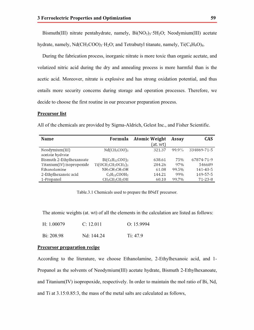
3 Ferroelectric Properties and Optimization 59
Bismuth(III) nitrate pentahydrate, namely, Bi(NO3)3·5H2O; Neodymium(III) acetate
hydrate, namely, Nd(CH3COO)3·H2O; and Tetrabutyl titanate, namely, Ti(C4H9O)4.
During the fabrication process, inorganic nitrate is more toxic than organic acetate, and
volatized nitric acid during the dry and annealing process is more harmful than is the
acetic acid. Moreover, nitrate is explosive and has strong oxidation potential, and thus
entails more security concerns during storage and operation processes. Therefore, we
decide to choose the first routine in our precursor preparation process.
Precursor list
All of the chemicals are provided by Sigma-Aldrich, Gelest Inc., and Fisher Scientific.
Table.3.1 Chemicals used to prepare the BNdT precursor.
The atomic weights (at. wt) of all the elements in the calculation are listed as follows:
H: 1.00079 C: 12.011 O: 15.9994
Bi: 208.98 Nd: 144.24 Ti: 47.9
Precursor preparation recipe
According to the literature, we choose Ethanolamine, 2-Ethylhexanoic acid, and 1-
Propanol as the solvents of Neodymium(III) acetate hydrate, Bismuth 2-Ethylhexanoate,
and Titanium(IV) isopropoxide, respectively. In order to maintain the mol ratio of Bi, Nd,
and Ti at 3.15:0.85:3, the mass of the metal salts are calculated as follows,
3 Ferroelectric Properties and Optimization 60
M[Nd(CH3COO)3]= 0.025 0.2 321.37 0.8599.9%
× × ×= 1.367 g
M[Bi(CH3COO)3]= 0.025 0.2 638.61 3.15 (1 10%)75%
× × × × += 14.752 g
M[Ti(OCH2CH2OCH3)3]= 0.025 0.2 284.26 397%
× × ×= 4.396 g
As shown in Fig 3.3, a detailed precursor preparation process can be described as
follows,
(1) 1.367 g Nd(CH3COO)3 is dissolved in NH2CH2CH2OH until 10 ml.
(2) 14.752 g Bi(CH3COO)3 is dissolved in C5H11COOH3 until 25 ml. Excess bismuth
nitrate of 10% is added to compensate the Bi loss during the thermal annealing process.
(3) 4.396 g Ti(OCH2CH2OCH3)3 is dissolved in CH3CH2CH2OH until 25 ml.
(4) Pour the Nd(CH3COO)3 solution into the Bi(CH3COO)3 solution, and clean the wall
of the beaker using CH3CH2CH2OH. Stir the mixed solution for 1 hr.
(5) Pour the Ti(OCH2CH2OCH3)3 solution into the as-prepared mixed solution, and
clean the wall of the beaker using CH3CH2CH2OH. Stir the mixed solution for 48 hrs.
(6) Add appropriate amount of CH3CH2CH2OH until 50 ml. Stir the mixed solution for
1 hr.
(7) Filter the as-prepared solution using a 0.2 μm filter and store the solution in a
conical beaker.
A photographic image of the as-prepared BNdT solution is shown in Fig 3.4; it can be
seen that a clear, uniform, and stable solution is achieved in our experiment.

3 Ferroelectric Properties and Optimization 61
Fig 3.3 Precursor preparation recipe.
Fig.3.4 A photographic image of the as-prepared BNdT solution.
3.2.3 Thin film fabrication
The fabrication process of the BNdT ferroelectric thin film can be concluded as follows.
(1) Substrate cleaning. A P-type (100) silicon wafer is ultrasonically cleaned using
hydrofluoric acid (HF), acetone, isopropanol, and deionized water, in that order, prior to
deposition. The hydrofluoric acid is introduced to remove the natural oxide layer on the

3 Ferroelectric Properties and Optimization 62
silicon wafer, and the acetone and isopropanol are used to remove the organic impurities
attached to the wafer surface. One thing to note is the order of the chemical cleaning:
since there might be some hydrogen dangling bonds introduced during the HF cleaning
process, the acetone, isopropanol, and deionized water cleaning must be done after the
HF cleaning so as to minimize the hydrogen dangling bonds generated in the previous
step.
(2) Thermal oxidization. 300 nm silicon dioxide (SiO2) is deposited on top of the
silicon wafer by a wet oxidation process at 1100°C.
(3) Bottom electrode sputtering. A bottom electrode consisting of a platinum (Pt) layer
of 200 nm and a titanium (Ti) layer of 30 nm is then deposited using a DC-sputtering
process. Since the Pt layer and SiO2 possess an intrinsic poor adhesiveness, the Ti layer is
applied to increase the adhesiveness between the Pt layer and SiO2 substrate, and thus
preventing the upper layer from being peeled-off in subsequent fabrication steps.
(4) Recovery annealing. The as-prepared platinum substrate is introduced to a rapid
thermal annealing (RTA) process (heating rate: 120 °C/s) at 650°C for 1 minute in an
oxygen atmosphere to remove the residual stress during the sputtering process.
(5) Spin coating deposition. The BNdT thin film is then deposited on top of the Pt(200
nm)/Ti(30 nm)/SiO2(300 nm)/Si(100) substrate, with a spin rate of 3000 rpm lasting for
30 s. This process is repeated until the desired thickness (300 nm) of the BNdT thin film
is obtained.
(6) Pyrogenation. The as-prepared BNdT thin film is left to a pyrogenation process at
380°C for 30 s in the air atmosphere, in order to help the organic solvent volatilize and
the ferroelectric crystallize.

3 Ferroelectric Properties and Optimization 63
(7) Pre-crystallization annealing. The BNdT thin film is introduced to a RTA process
in an oxygen atmosphere. The temperature quickly rises from room temperature to 200°C
where it is kept for 20 s, and then increases up to 650°C in 3.9 s (heating rate:110°C/s)
and is held for a further 60 s.
(8) Crystallization annealing. After processes (5) to (7) have been repeated an
appropriate amount of times, a crystallization annealing process is applied to the as-
prepared BNdT thin films. Different annealing temperatures of 300°C, 400°C, 500°C,
and 650°C, for 45 min in an oxygen atmosphere, are investigated to seek an optimized
fabrication recipe for the BNdT thin film.
(9) Top electrode sputtering. Top Pt electrodes are introduced by means of DC
magnetron sputtering with a shadow mask. The diameter of the top electrode is typically
200 μm.
The as-prepared BNdT thin film demonstrates a neat and clear surface, which can be
evaluated by the Keyence photographic image (as shown in Fig 3.5) and scanning
electron microscope (SEM) image (as shown in Fig 3.6). More advanced structure and
performance characterization methodologies will be examined in the coming sections.
Fig 3.5 Keyence photographic image of the upper electrode in the as-prepared BNdT thin film.
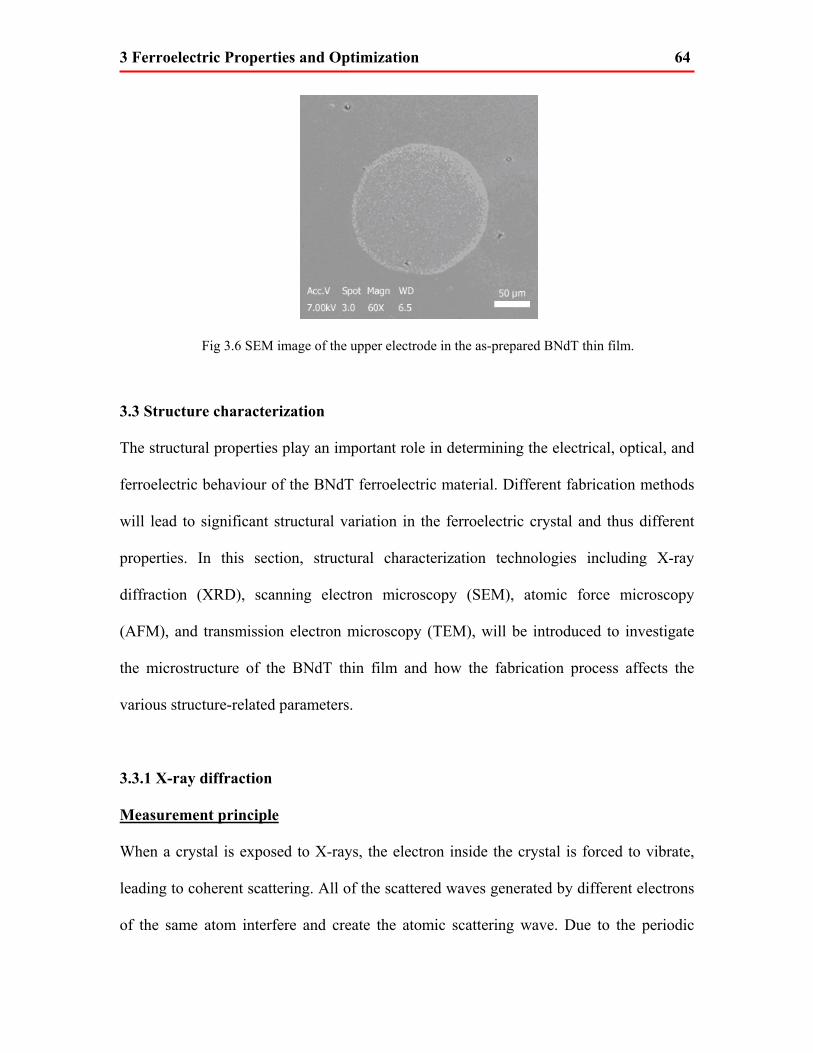
3 Ferroelectric Properties and Optimization 64
Fig 3.6 SEM image of the upper electrode in the as-prepared BNdT thin film.
3.3 Structure characterization
The structural properties play an important role in determining the electrical, optical, and
ferroelectric behaviour of the BNdT ferroelectric material. Different fabrication methods
will lead to significant structural variation in the ferroelectric crystal and thus different
properties. In this section, structural characterization technologies including X-ray
diffraction (XRD), scanning electron microscopy (SEM), atomic force microscopy
(AFM), and transmission electron microscopy (TEM), will be introduced to investigate
the microstructure of the BNdT thin film and how the fabrication process affects the
various structure-related parameters.
3.3.1 X-ray diffraction
Measurement principle
When a crystal is exposed to X-rays, the electron inside the crystal is forced to vibrate,
leading to coherent scattering. All of the scattered waves generated by different electrons
of the same atom interfere and create the atomic scattering wave. Due to the periodic

3 Ferroelectric Properties and Optimization 65
manner of the atoms inside the crystal, all atomic scattering waves exhibit a set phase
difference, and thus interfere with each other. In some specific directions, constructive
interference occurs, resulting in a diffracted wave. Therefore, the diffracted wave of the
crystal comes from the superposition of the atomic scattering waves.
XRD is based on the measurement of the diffracted wave of the crystal, as stimulated
by external X-ray radiation. The diffraction direction and diffraction intensity are two
important parameters in such an analysis. The XRD analysis method is non-destructive,
and the diffraction patterns can offer following information regarding the as-measured
crystal:
(1) Qualitative phase analysis,
(2) Quantitative phase analysis,
(3) Degree of crystallinity analysis,
(4) Residual stress analysis,
(5) Grain size and distribution analysis,
(6) Orientation and structural analysis.
Measurement parameter configuration
Instrument: X-Ray Diffractometer (Philips PW1710, Holland) with Cu Kα radiation
Parameter configuration: At Normal Pressure and Temperature (NPT), due to the
existence of silicon substrate in the BNdT sample, the strong single crystal diffraction
will damage the diffractometer. Therefore, the scan angle (2θ) is set from 5° to 65° so as
to skip over the silicon diffraction peak in our experiment.
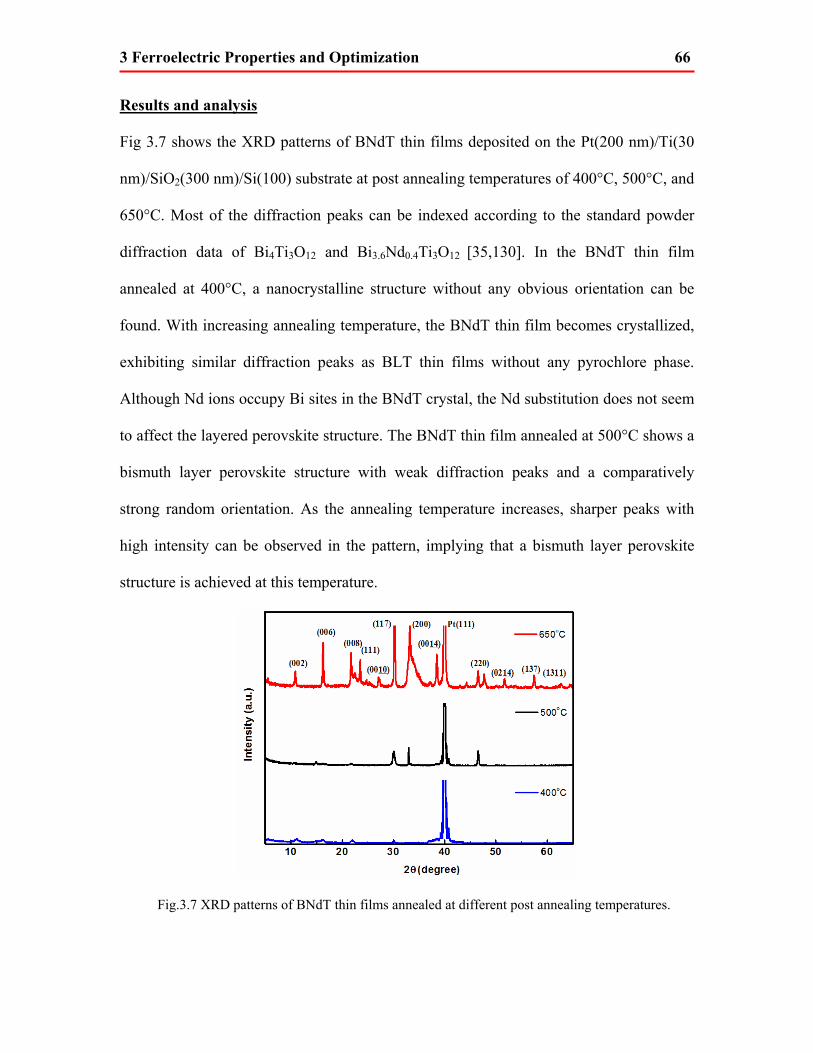
3 Ferroelectric Properties and Optimization 66
Results and analysis
Fig 3.7 shows the XRD patterns of BNdT thin films deposited on the Pt(200 nm)/Ti(30
nm)/SiO2(300 nm)/Si(100) substrate at post annealing temperatures of 400°C, 500°C, and
650°C. Most of the diffraction peaks can be indexed according to the standard powder
diffraction data of Bi4Ti3O12 and Bi3.6Nd0.4Ti3O12 [35,130]. In the BNdT thin film
annealed at 400°C, a nanocrystalline structure without any obvious orientation can be
found. With increasing annealing temperature, the BNdT thin film becomes crystallized,
exhibiting similar diffraction peaks as BLT thin films without any pyrochlore phase.
Although Nd ions occupy Bi sites in the BNdT crystal, the Nd substitution does not seem
to affect the layered perovskite structure. The BNdT thin film annealed at 500°C shows a
bismuth layer perovskite structure with weak diffraction peaks and a comparatively
strong random orientation. As the annealing temperature increases, sharper peaks with
high intensity can be observed in the pattern, implying that a bismuth layer perovskite
structure is achieved at this temperature.
Fig.3.7 XRD patterns of BNdT thin films annealed at different post annealing temperatures.

3 Ferroelectric Properties and Optimization 67
C-axis oriented peaks such as (004), (006), (008), and (0014), can be found in the
BNdT thin film processed at 650°C. In order to estimate the degree of preferred
orientation, the volume fraction α(00l) of c-axis-oriented grains in the BNdT thin film can
be defined as: [131,132]
(00 ) (00 ) / ( )i il
i iI l I hkα =∑ ∑ l (3.1)
where I(hkl) is the measured intensity of the (hkl) peaks for the thin film. The α(00l) values
obtained at the three different temperature are: 15.8%, 21.4%, and 44.7%, respectively,
indicating a remarkable increase of c-axis-oriented grains in the thin films with increasing
annealing temperature. The BNdT thin film annealed at 650°C possesses an α(00l) of
44.7%, indicating a preferred c-axis orientation. As reported by Chon et al. [34] such
highly orientated BNdT thin films will exhibit good ferroelectric properties.
Assuming that the BNdT thin film has an orthorhombic structure, the lattice
parameters of the BNdT thin film can be calculated to be a=5.413 Å, b=5.285 Å,
c=32.916 Å, compared with the lattice parameters of the Bi3.6Nd0.4Ti3O12 (a=5.429 Å,
b=5.406 Å, c=32.832 Å), indicating that the substituted Nd ions do not affect the
perovskite structure of the crystal.
3.3.2 Scanning electron microscope
Measurement principle
In the SEM characterization, an ultra-narrow electron beam scans a test sample. Many
secondary electrons are stimulated around the surface of the sample, and the amount of
secondary electrons is determined by the incidence angle of the electron beam. In other
words, the amount of the secondary electrons is determined by the surface structure of the

3 Ferroelectric Properties and Optimization 68
sample. Secondary electrons will be collected by a specific detector and changed into an
optical signal by a photoelectric converter. Then, the optical signal will be amplified and
converted back to an electrical signal to control the intensity of the electron beam on the
fluorescent screen, resulting in a scanning pattern image that is synchronous with the
electron beam. In order to increase the emission efficiency of the secondary electron, and
thus increase the imaging quality, a heavy metal atom such as Au or Cr will be coated on
top of the sample’s surface before the SEM measurement.
Measurement parameter configuration
Instrument: Field-emission scanning electron microscopy (Hitachi S-4700, Japan)
Parameter configuration: The SEM measurement is classified in two segments,
namely, cross section analysis and top-view analysis. The cross section analysis is used to
examine the longitudinal performance of the multilayer, such as consistence and
compactness. On the other hand, the top-view analysis reveals the surface properties of
the sample including smoothness, flatness, and uniformity.
After cutting the sample into an appropriate size (1cm*1cm), a thin layer of amorphous
Cr is coated using a DC-sputtering process. The thickness of the Cr layer is estimated to
be 0.05 nm/s*300s = 15 nm.
Results and analysis
Fig. 3.8 shows the cross section SEM micrograph of the BNdT thin film annealed at
650°C, exhibiting a clear and sharp boundary between different layers. We conclude that
a dense and smooth film is achieved and the film thickness is estimated to be 300 nm in
this measurement. The surface morphology of the same sample can be seen from Fig.3.9,
indicating that the perovskite layer was oriented randomly and that the surface is uniform
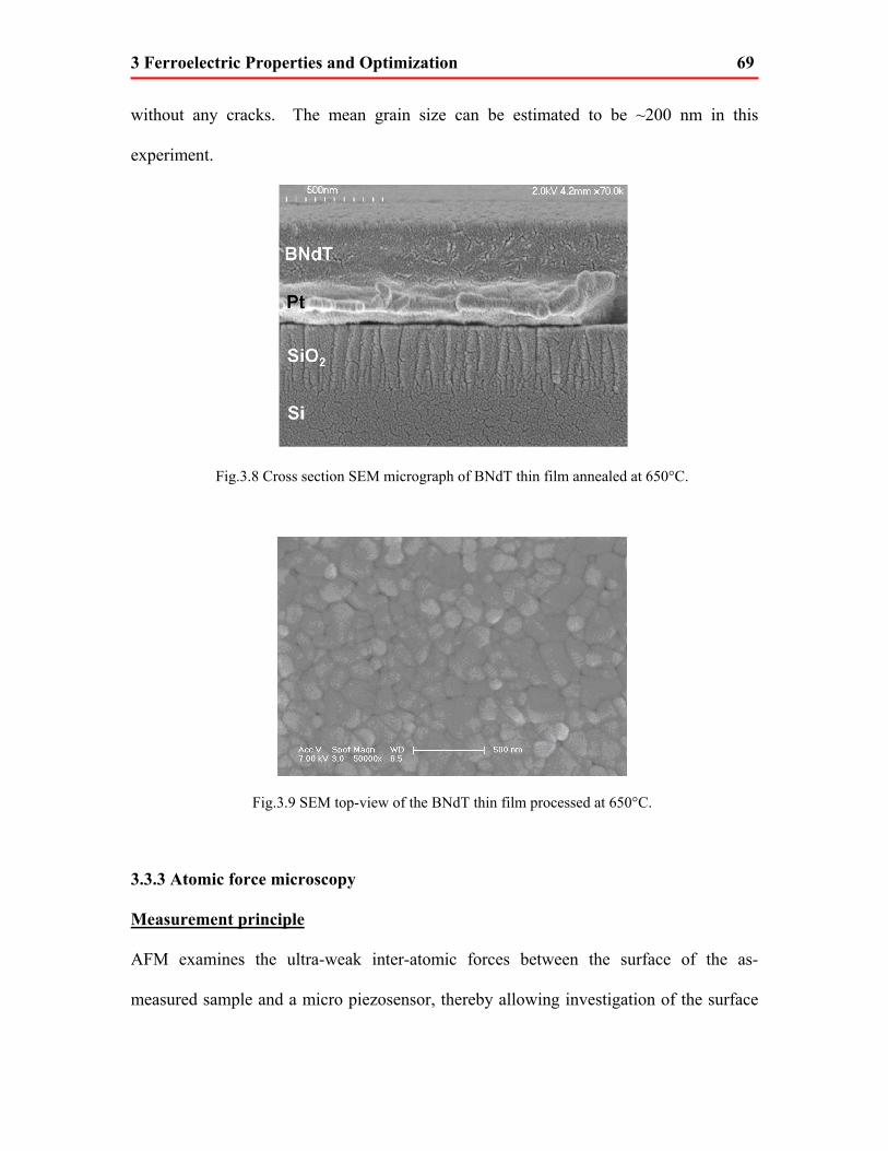
3 Ferroelectric Properties and Optimization 69
without any cracks. The mean grain size can be estimated to be ~200 nm in this
experiment.
Fig.3.8 Cross section SEM micrograph of BNdT thin film annealed at 650°C.
Fig.3.9 SEM top-view of the BNdT thin film processed at 650°C.
3.3.3 Atomic force microscopy
Measurement principle
AFM examines the ultra-weak inter-atomic forces between the surface of the as-
measured sample and a micro piezosensor, thereby allowing investigation of the surface

3 Ferroelectric Properties and Optimization 70
structure and properties. In general, during the AFM measurement, a microprobe is
placed on one end of an elastic micro-cantilever beam, while the other end of the micro-
cantilever beam is fixed. When the probe scans over the surface of the sample, the atomic
repulsion between the probe and the surface of the sample will cause a tiny distortion in
the micro-cantilever beam. Such distortion in the micro-cantilever beam can be regarded
as an indirect measure of the atomic repulsion between the probe and the surface of the
sample. A laser beam reflected off the back of the micro-cantilever beam is guided into a
photodetector. It can precisely measure the tiny distortion of the micro-cantilever beam
and thus the surface topography of the sample can be indirectly reflected by the repulsion
between the probe and the surface of the sample.
Measurement parameter configuration
Instrument: Atomic force microscopy (Dimension/Veeco 3100, USA).
Parameter configuration: At NPT, the sample is prepared into an appropriate size
(2cm*2cm), and the measurement range is ~2.5 nm*2.5 nm.
Results and analysis
Fig.3.10 (a)-(d) shows the AFM surface morphologies of BNdT thin films annealed at
different temperatures. A smooth and uniform surface is observed and the BNdT thin film
is seen to be composed of close-packed spherical grains. The grain size measured
increases remarkably with increasing post annealing temperatures, from 79 nm at 300°C
to 202 nm at 650°C, in agreement with the sol-gel derived BNdT thin film reported by J.
H. Li et al. [129]. The surface roughness (Ra) of the 250 nm BNdT thin film also
increases with increasing post annealing temperature as follows: Ra is 1.77 nm, 2.36 nm,
2.79 nm, and 3.90 nm, for the samples annealed at 300°C, 400°C, 500°C, and 650°C,

3 Ferroelectric Properties and Optimization 71
respectively. The surface roughness variations and the grain size changes are consistent
with the results reported by G. Jang et al., [133] C. P. Luo et al., [134] X. Z. Ding et al.,
[135] and can be corroborated by the increase of peak sharpness in XRD patterns shown
in Fig.3.7.
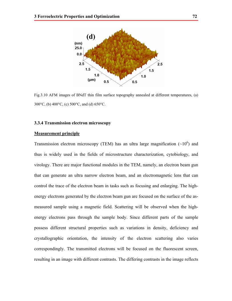
3 Ferroelectric Properties and Optimization 72
Fig.3.10 AFM images of BNdT thin film surface topography annealed at different temperatures, (a)
300°C, (b) 400°C, (c) 500°C, and (d) 650°C.
3.3.4 Transmission electron microscopy
Measurement principle
Transmission electron microscopy (TEM) has an ultra large magnification (~106) and
thus is widely used in the fields of microstructure characterization, cytobiology, and
virology. There are major functional modules in the TEM, namely, an electron beam gun
that can generate an ultra narrow electron beam, and an electromagnetic lens that can
control the trace of the electron beam in tasks such as focusing and enlarging. The high-
energy electrons generated by the electron beam gun are focused on the surface of the as-
measured sample using a magnetic field. Scattering will be observed when the high-
energy electrons pass through the sample body. Since different parts of the sample
possess different structural properties such as variations in density, deficiency and
crystallographic orientation, the intensity of the electron scattering also varies
correspondingly. The transmitted electrons will be focused on the fluorescent screen,
resulting in an image with different contrasts. The differing contrasts in the image reflects
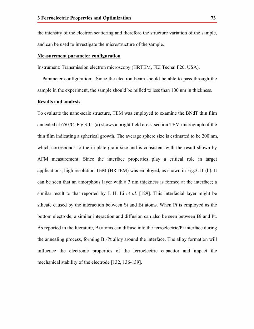
3 Ferroelectric Properties and Optimization 73
the intensity of the electron scattering and therefore the structure variation of the sample,
and can be used to investigate the microstructure of the sample.
Measurement parameter configuration
Instrument: Transmission electron microscopy (HRTEM, FEI Tecnai F20, USA).
Parameter configuration: Since the electron beam should be able to pass through the
sample in the experiment, the sample should be milled to less than 100 nm in thickness.
Results and analysis
To evaluate the nano-scale structure, TEM was employed to examine the BNdT thin film
annealed at 650°C. Fig.3.11 (a) shows a bright field cross-section TEM micrograph of the
thin film indicating a spherical growth. The average sphere size is estimated to be 200 nm,
which corresponds to the in-plate grain size and is consistent with the result shown by
AFM measurement. Since the interface properties play a critical role in target
applications, high resolution TEM (HRTEM) was employed, as shown in Fig.3.11 (b). It
can be seen that an amorphous layer with a 3 nm thickness is formed at the interface; a
similar result to that reported by J. H. Li et al. [129]. This interfacial layer might be
silicate caused by the interaction between Si and Bi atoms. When Pt is employed as the
bottom electrode, a similar interaction and diffusion can also be seen between Bi and Pt.
As reported in the literature, Bi atoms can diffuse into the ferroelectric/Pt interface during
the annealing process, forming Bi-Pt alloy around the interface. The alloy formation will
influence the electronic properties of the ferroelectric capacitor and impact the
mechanical stability of the electrode [132, 136-139].

3 Ferroelectric Properties and Optimization 74
Fig.3.11 (a) TEM micrograph of the BNdT thin film deposited on Si substrate. (b) High resolution
TEM image of the BNdT thin film deposited on Si substrate.
3.4 Ferroelectric properties characterization
3.4.1 Remnant polarization
Research into ferroelectric properties is the principle part of the BNdT ferroelectric thin
film investigation, and the remnant polarization plays an important role in such properties.
As a crucial parameter of ferroelectrics, almost all ferroelectric properties can be
reflected in the ferroelectric hysteresis loop. Important ferroelectric parameters such as
the remnant polarization and coercive field can both be extracted from examination of the
hysteresis loop.
According to the literature, the most significant advantage of the BNdT thin film is the
remarkable remnant polarization value compared with traditional ferroelectrics such as
PZT and SBT. Fabrication methods can impact the ferroelectric remnant polarization
significantly. As reported by T. Kojima et al. [140], BNdT deposited by the MOCVD
method possesses a remnant polarization of ~25 μC/cm2, while MOD derived BNdT can

3 Ferroelectric Properties and Optimization 75
exhibit a remnant polarization of >56 μC/cm2. Meanwhile, the annealing temperature also
plays a key role in determining the remnant polarization of the BNdT thin film. In this
section, the variation of BNdT remnant polarization for different annealing temperatures
is demonstrated and investigated.
Fig.3.12 shows the polarization-voltage (PV) hysteresis loops of the BNdT thin film
capacitors with different annealing temperatures in an oxygen atmosphere. It can be
concluded that the remnant polarization (2Pr) increases with increasing annealing
temperature from 400°C to 650°C. In the BNdT sample processed at 650°C, a well
established hysteresis loop is obtained exhibiting a remnant polarization (2Pr) of 39.6
μC/cm2 and a coercive field of 85 kV/cm with an applied voltage of 5 V, which is much
larger than for with BNdT prepared by RF magnetron sputtering (~13.2 μC/cm2) [133]
and chemical solution deposition (~21 μC/cm2) [141]. This result indicates that 650°C is
an optimized annealing temperature, and it can help the crystallization process of the
BNdT ferroelectric thin film. All of the forthcoming research will be conducted based on
the 650°C processed samples.
Fig. 3.12 Ferroelectric hysteresis loops of BNdT thin films annealed at different temperatures.
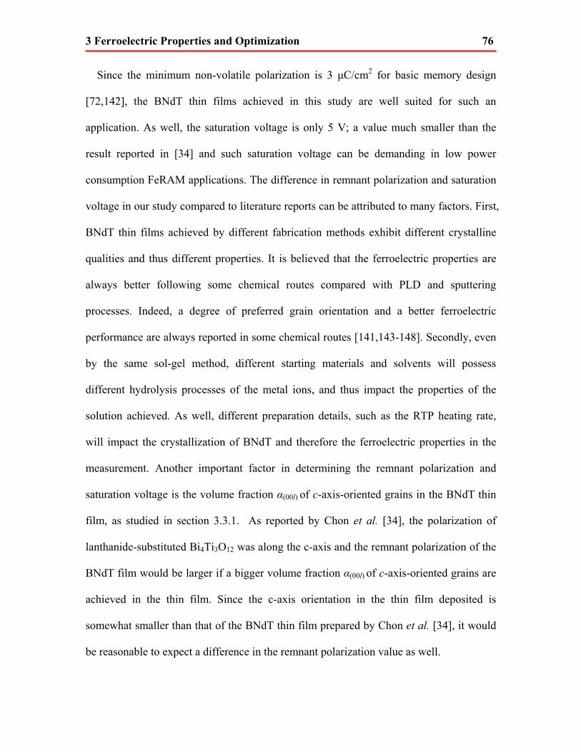
3 Ferroelectric Properties and Optimization 76
Since the minimum non-volatile polarization is 3 μC/cm2 for basic memory design
[72,142], the BNdT thin films achieved in this study are well suited for such an
application. As well, the saturation voltage is only 5 V; a value much smaller than the
result reported in [34] and such saturation voltage can be demanding in low power
consumption FeRAM applications. The difference in remnant polarization and saturation
voltage in our study compared to literature reports can be attributed to many factors. First,
BNdT thin films achieved by different fabrication methods exhibit different crystalline
qualities and thus different properties. It is believed that the ferroelectric properties are
always better following some chemical routes compared with PLD and sputtering
processes. Indeed, a degree of preferred grain orientation and a better ferroelectric
performance are always reported in some chemical routes [141,143-148]. Secondly, even
by the same sol-gel method, different starting materials and solvents will possess
different hydrolysis processes of the metal ions, and thus impact the properties of the
solution achieved. As well, different preparation details, such as the RTP heating rate,
will impact the crystallization of BNdT and therefore the ferroelectric properties in the
measurement. Another important factor in determining the remnant polarization and
saturation voltage is the volume fraction α(00l) of c-axis-oriented grains in the BNdT thin
film, as studied in section 3.3.1. As reported by Chon et al. [34], the polarization of
lanthanide-substituted Bi4Ti3O12 was along the c-axis and the remnant polarization of the
BNdT film would be larger if a bigger volume fraction α(00l) of c-axis-oriented grains are
achieved in the thin film. Since the c-axis orientation in the thin film deposited is
somewhat smaller than that of the BNdT thin film prepared by Chon et al. [34], it would
be reasonable to expect a difference in the remnant polarization value as well.

3 Ferroelectric Properties and Optimization 77
Since the operation frequency is an important performance parameter in many
electrical and optical applications, the frequency dependence of the polarization-voltage
(PV) hysteresis loops is also investigated, as shown in Fig. 3.13. It can be seen that the
remnant polarization values and the saturation of loops decrease significantly with an
increase in operation frequency. This can be explained by the nature of ferroelectricity. In
ferroelectrics, the remnant polarization field is created by an external electric field.
However, the variation of remnant polarization field does not occur simultaneously with
that of the external electric field. Such hysteretic behaviour can be observed through the
existence of remnant polarization when the external electric field is removed. Since there
is a hysteretic behaviour between the remnant polarization field and the external electric
field, the variation of external electric field cannot be too rapid. Otherwise, the remnant
polarization field will not be able to catch up with the external electric field, and there
will be degradation in the ferroelectric properties due to the ferroelectric relaxation
phenomenon. In Fig. 3.13, it can be seen that in the 100 Hz frequency region, the external
electric field varies within the ferroelectric relaxation, and the polarization dipoles in the
BNdT crystal have sufficient response time to be set along the polaxis and thus exhibit a
high remnant polarization value. Increasing the measurement frequency to 1 KHz, the
kinetics of polarization reversal of the BNdT thin film becomes unable to follow the
increase in measurement frequency, and ferroelectric degradation is then observed.
Actually, most ferroelectric materials reveal well-defined performance in such a high
frequency application. As introduced earlier in this section, a polarization of 3 μC/cm2 is
adequate for non-volatile applications. Since the remnant polarization is higher than
necessary but the operational frequency is relatively low, a trade-off such as increasing
3 Ferroelectric Properties and Optimization 78
the frequency with a reasonable sacrifice in remnant polarization, can make this material
feasible for modern usage.
Fig. 3.13 Ferroelectric hysteresis loops of the BNdT thin films measured at different frequencies from
100 Hz to 2 KHz.
3.4.2 Fatigue properties
The BNdT ferroelectric exhibits a superb fatigue endurance compared with traditional
ferroelectric PZT [149]. Reported by Chon et al. [34], with an applied voltage of 5 V,
BNdT exhibits <2% degradation in remnant polarization and <1.5% degradation in
coercive field after 6.5×10¹⁰ switching cycles. In this section, we will investigate the
fatigue performance of the BNdT ferroelectric, and the fatigue variation with different
test frequencies and test amplitudes.
Fig. 3.14 (a) and (b) shows the BNdT polarization as a function of the polarization
switching cycles at 2.5 V/10 MHz and 2.5 V/1 MHz. It can be seen that in the 2.5 V/10
MHz test case, the BNdT thin film exhibits good fatigue properties, and little fatigue
degradation in remnant polarization (<1.5%) and coercive field (<1.6%) is demonstrated

3 Ferroelectric Properties and Optimization 79
under 1×10¹⁰ switching cycles; indicating that a good fatigue endurance for the BNdT
thin film is achieved in this experiment. However, in the 2.5 V/1 MHz test case, >29.4%
degradation in remnant polarization and 12.7% degradation in coercive field are observed.
Fig. 3.14 Fatigue curves of polarization as a function of switching cycles at (a) 2.5 V/1 MHz and (b)
2.5 V/10 MHz.
Such a frequency dependence of the ferroelectric fatigue can be explained by the
ferroelectric domains reorientation effect. Due to the nature of remnant polarization, the
ferroelectric domains re-orient to a preferred direction when an external electrical field is
applied. This results in the redistribution of crystalline lattice stress, which can be
characterized by an atomic force analysis. As reported by N. X. Zhang et al. [150], the

3 Ferroelectric Properties and Optimization 80
external electric field plays an important role in the ferroelectric domains re-orientation
process, and only external electric fields meeting certain criteria can cause the re-
orientation. The minimum electric field Emin required for ferroelectric domain re-
orientation, and the switching time τs, should satisfy the following relationship [151],
E ≥ Emin=ζ(τs)α , (3.2)
where ζ and α are two set empirical constants derived in the experiment.
It can be seen that given a fixed external electrical field Eγ and a switching time τγ, the
switching frequency 1/τγ can be calculated; and any external electric field with frequency
higher than 1/τγ cannot cause ferroelectric domain re-orientation. Therefore, application
in this frequency range will cause little fatigue degradation. Hence, from an application
point of view, the higher operational frequency a material can reach, the more application
prospects it will have. As discussed in section 3.3.1, we can sacrifice some remnant
polarization of the BNdT ferroelectric in order to increase the operational frequency. This
compromise not only expands the potential application fields, but also skips the “fatigue
frequency interval” and as such is a method that achieves both goals simultaneously.
The amplitude dependence of the BNdT fatigue variation is shown in Fig. 3.15 (a) and
(b). It can be seen that under polarization switching cycles at 2 V/10 MHz and 3 V/1
MHz, BNdT demonstrated a similar fatigue performance (<1.5%). This can also be
explained by Eq.3.2. Since there is no amplitude term in the equation, the amplitude of
the external electric field does not affect determination of the fatigue degradation of the
BNdT thin film.

3 Ferroelectric Properties and Optimization 81
Fig. 3.15 Fatigue curves of polarization as a function of switching cycles at (a) 3 V/10 MHz and (b) 2
V/10 MHz.
3.4.3 Leakage properties
The large remnant polarization in the BNdT thin film can be attributed to the good
interaction properties of the BNdT ferroelectric thin film and the Pt substrate. As studied
in section 3.3.4, the amorphous inter-diffusion is only 3 nm in thickness between the
BNdT ferroelectric thin film and the Pt substrate, indicating a well-defined interface
property.

3 Ferroelectric Properties and Optimization 82
Leakage properties can also allow examination of the interface behaviour of the
BNdT/Pt capacitor. The leakage current density of the BNdT thin film is measured to be
5×10⁻⁷ A/cm2 at an applied voltage of 5 V, as shown in Fig. 3.16, indicating a fairly low
leakage density.
Fig.3.16. IV curves of BNdT thin film annealed at 650°C.
Such a leakage density value is desirable in FeRAM and FeFET related applications. A
low leakage density indicates a slow discharge process and thus a strong charge retention
endurance. In the FeFET application, charge retention endurance plays a significant role
in determining the reliability and lifetime of the memory device. In fact, there has been
significant research reported towards further increasing the leakage properties of the
ferroelectric capacitor and thus improving the reliability and lifetime of the applications.
Buffer layer technology, for example, has been regarded as an effective method for
increasing the retention properties. By inserting an ultra thin dielectric buffer layer such
as HfO2, ZnO, or SrTiO3, between the ferroelectric thin film and the substrate, the high-K
essence of these buffer layers will further prevent inter-diffusion between the
ferroelectric layer and the substrate, and increase the leakage endurance of the

3 Ferroelectric Properties and Optimization 83
ferroelectric structure. Moreover, some buffer layers with ABO3 structures possess a
similar lattice constant with ferroelectric crystal, and will help the crystallization process
of the upper ferroelectric thin film.
3.5 Doping methodologies and optimization
In the previous section, we discussed the variation of ferroelectric structural and electrical
properties for different annealing temperatures. Actually, since the BNdT ferroelectric is
Nd doped bismuth titanate in nature; different Nd doping concentrations can also
modulate the structural and ferroelectric properties in the application. Since the major
application concern of the BNdT thin film is the ferroelectric remnant polarization and
Bi3.15Nd0.85Ti3O12 is proven to possess the largest 2Pr value, Bi4-xNdxTi3O12 (x=0.85) is
always utilized in memory based ferroelectric research. However, different Nd doping
concentrations and their impact on structural properties have not been widely reported in
the literature. In this section, we fabricate Bi4-xNdxTi3O12 (x=0, 0.25, 0.5, and 0.85)
materials with different Nd contents, and report the dependence of the Bi4-xNdxTi3O12
structural properties on the Nd content. Our work indicates that Nd substitution can be
utilized to tune and modify the structural parameters of Bi4-xNdxTi3O12 in ferroelectric-
based applications.
3.5.1 Bi4-xNdxTi3O12 ferroelectric thin film fabrication
Precursor preparation recipe
In a procedure comparable to that described in section 3.2.1, we choose a similar recipe
to fabricate the Bi4-xNdxTi3O12 (x=0, 0.25, 0.5, and 0.85) precursors.

3 Ferroelectric Properties and Optimization 84
In order to maintain the desired mol ratio of Bi, Nd, and Ti, the corresponding mass of
all the metal salts are calculated as follows,
(1) x=0, Bi4Ti3O12
M[Nd(CH3COO)
3]= 0.025 0.2 321.37 0
99.9%× × ×
= 0 g
M[Bi(CH3COO)3]= 0.025 0.2 638.61 4 (1 10%) 18.73375%
× × × × += g
M[Ti(OCH2CH
2OCH
3)
3]= 0.025 0.2 284.26 3
97%× × ×
= 4.395g
(2) x=0.25, Bi3.75Nd0.25Ti3O12
M[Nd(CH3COO)
3]= 0.025 0.2 321.37 0.25
99.9%× × ×
= 0.402 g
M[Bi(CH3COO)3]= 0.025 0.2 638.61 3.75 (1 10%) 17.56275%
× × × × += g
M[Ti(OCH2CH
2OCH
3)
3]= 0.025 0.2 284.26 3
97%× × ×
= 4.395g
(3) x=0.5 Bi3.5Nd0.5Ti3O12
M[Nd(CH3COO)
3]= 0.025 0.2 321.37 0.5
99.9%× × ×
= 0.804 g
M[Bi(CH3COO)3]= 0.025 0.2 638.61 3.5 (1 10%) 16.39175%
× × × × += g
M[Ti(OCH2CH
2OCH
3)
3]= 0.025 0.2 284.26 3
97%× × ×
= 4.395g
(4) x=0.85 Bi3.15Nd0.85Ti3O12
M[Nd(CH3COO)3]= 0.025 0.2 321.37 0.8599.9%
× × ×= 1.367 g

3 Ferroelectric Properties and Optimization 85
M[Bi(CH3COO)3]= 0.025 0.2 638.61 3.15 (1 10%)75%
× × × × += 14.752 g
M[Ti(OCH2CH2OCH3)3]= 0.025 0.2 284.26 397%
× × ×= 4.396 g
Excess bismuth nitrate of 10% is added in all of the precursors to compensate the Bi
loss during the thermal annealing process.
Fabrication process
Similar to the procedure described in section 3.2.3, Pt(200 nm)/Ti(30 nm)/SiO2(300
nm)/Si(100) was introduced as the substrate and ultrasonically cleaned in acetone,
isopropanol, and deionized water prior to deposition. The spin rate was 3000 rpm, lasting
for half a minute for each step. The as-deposited BNdT films were introduced to a rapid
thermal annealing (RTA) process (heating rate: 120°C/s) at 650°C for 1 minute in oxygen
atmosphere. To obtain the desired thickness, the spin coating process was repeated
several times. The as-deposited BNdT films were then introduced to a rapid thermal
annealing (RTA) process at 600°C for 10 minutes in the air.
3.5.2 Bi4-xNdxTi3O12 structure analysis
Fig.3.17 (a)-(d) shows the surface topography of the BNdT thin films measured by
atomic force microscopy (AFM). Smooth and uniform surfaces and close-packed
spherical grains can be observed in all BNdT samples. The mean grain size decreases
from 190 to 80 nm with increasing Nd substitution content; indicating a suppression of
crystal upon Nd substitution.
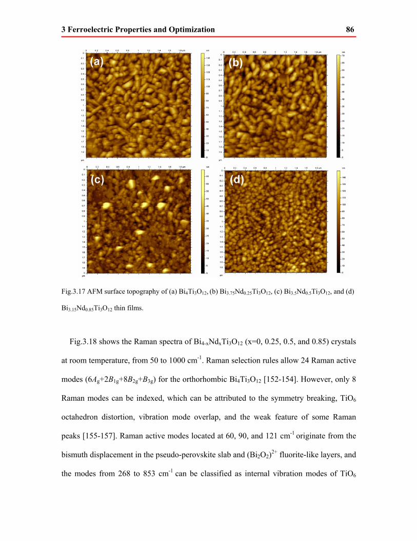
3 Ferroelectric Properties and Optimization 86
Fig.3.17 AFM surface topography of (a) Bi4Ti3O12, (b) Bi3.75Nd0.25Ti3O12, (c) Bi3.5Nd0.5Ti3O12, and (d)
Bi3.15Nd0.85Ti3O12 thin films.
Fig.3.18 shows the Raman spectra of Bi4-xNdxTi3O12 (x=0, 0.25, 0.5, and 0.85) crystals
at room temperature, from 50 to 1000 cm-1. Raman selection rules allow 24 Raman active
modes (6Ag+2B1g+8B2g+B3g) for the orthorhombic Bi4Ti3O12 [152-154]. However, only 8
Raman modes can be indexed, which can be attributed to the symmetry breaking, TiO6
octahedron distortion, vibration mode overlap, and the weak feature of some Raman
peaks [155-157]. Raman active modes located at 60, 90, and 121 cm-1 originate from the
bismuth displacement in the pseudo-perovskite slab and (Bi2O2)2+ fluorite-like layers, and
the modes from 268 to 853 cm-1 can be classified as internal vibration modes of TiO6

3 Ferroelectric Properties and Optimization 87
octahedral of perovskite unit [156,158]. Moreover, the internal modes of 268 and 329 cm-
1 can be attributed to the O-Ti-O bending, while the mode at 853 cm-1 is caused by the Ti-
O symmetric stretching of TiO6 octahedral, and the Raman modes at 552 and 627 cm-1
can be ascribed to the combination of bending and stretching of TiO6 octahedral [154].
Fig.3.18 Raman scattering spectrum of Bi4-xNdxTi3O12 (x=0, 0.25, 0.5, and 0.85) thin films.
It can be seen that Raman modes at 90 and 121 cm-1 corresponding to the Bi mode in
(Bi2O2)2+ layers become broad and soft with high Nd substitution content, indicating an
increased lattice distortion due to the substitution of Bi with Nd atoms. However, no
obvious mode shift is observed in this region, showing that the Nd additive stays mainly
inside the perovskite units and does not incorporate into the fluorite-like layers
[144,154,158]. Meanwhile, significant changes can be indexed at modes from 268 to 853
cm-1 with the increase of Nd doping concentration, such as the shift of the mode at 268
cm-1, and the broadening and softening of the modes at 268, 552, and 853 cm-1, indicating
tilting and distortion in TiO6 octahedral and more difficulty in achieving perovskite phase
with increased Nd content [156,158].

3 Ferroelectric Properties and Optimization 88
3.6 Conclusion
In this chapter, we demonstrated the fabrication process and properties characterization of
the BNdT ferroelectric thin film. From the precursor preparation to the sol-gel/spin
coating fabrication, and from the structural characterization to the ferroelectric
investigation, the fabrication dependence of BNdT properties were investigated in detail.
An optimized fabrication process was obtained based on previous research, and will be
further applied in the coming chapters. Bi4-xNdxTi3O12 thin films with different Nd doping
concentrations were also prepared to study the dependence of BNdT properties on Nd
doping concentration.

4 Optical Properties of Ferroelectrics and their Optimization 89
Chapter 4
Optical Properties of Ferroelectrics and
their Optimization
4.1 Introductio
ince the first report by Chon et al. [34], there has been much research done
examining the electrical properties of BNdT ferroelectric thin films,
confirming the advantages of using this material in electrical-domain
applications [35-37]. However, so far little attention has been paid to the optical
properties of the BNdT material. There was one report regarding the band gap energy
fitting from an ellipsometer measurement [38], which provided a basic theoretical
understanding of the optical properties of the BNdT material. However, a detail optical
investigation including parameters such as transmittance T, refractive index n, extinction
coefficient k, etc. was not entirely done. To the best of our knowledge, there has been no
systematic investigation of the optical properties of the BNdT material. Furthermore,
different impact mechanisms such as the crystallization temperature, quantum scale, and
ingredient substitution on the BNdT thin film optical properties are never investigated. In
this chapter, we present the first experimental study on the subject, and provide a useful
S n
4 Optical Properties of Ferroelectrics and their Optimization 90
understanding of the correlation between different impact mechanisms and the optical
properties of BNdT thin films.
The remainder of this chapter is organized as follows. Section 4.2 introduces three
different impact mechanisms on the optical properties of BNdT thin film, and discusses
the physical nature of these impact mechanisms. From Sections 4.3 to 4.5, we
independently evaluate the effect of these three impact mechanisms on the BNdT optical
properties. More specifically, Section 4.3 explores the dependence of the BNdT optical
parameters on the crystallization temperature such as the transmittance spectrum,
refractive index, extinction coefficient, and band gap energy. In Section 4.4, the impact of
quantum scale is presented and investigated. Section 4.5 continues this research by
testing scenarios of different Nd ingredient substitution. Finally, this chapter is
summarized and concluded in Section 4.6.
4.2 Three different mechanisms
Optical properties are an intrinsic part of all ferroelectric materials. The optical behaviour
is determined by the material itself and by the microstructure of the as-prepared samples.
Different materials possess different optical properties; for example, PZT and SBT
materials exhibit different refractive indexes and EO coefficients, and thus have different
application prospects. Even within the same material, optical properties may exhibit
significant variations due to different fabrication approaches. As explained in the
previous section, different fabrication methods will provide obvious differences in crystal
quantity, residual stress, lattice constant, etc., and will thusly impact the properties of the
material in optical applications. In general, microstructure plays an important role in

4 Optical Properties of Ferroelectrics and their Optimization 91
determining the properties of the ferroelectric material. As discussed in the previous
chapter, the ferroelectric properties are significantly affected by the microstructure of the
material itself; similarly, the optical properties of the ferroelectric thin film are also
impacted. There are three major mechanisms that can be involved when researching the
optical properties of the BNdT ferroelectric thin film, namely, crystallization temperature,
quantum scale, and ingredient substitution.
4.2.1 Crystallization temperature
As a critical fabrication parameter, the crystallization process directly determines the
growth and properties of the BNdT ferroelectric material. During the crystallization
process, the ferroelectric material transforms from an amorphous phase to the desired
perovskite phase [132]. The annealing temperature and annealing time determine the
transformation rate and efficiency. If the annealing temperature is too low, the BNdT will
end up with pyrochlore phase rather than perovskite phase [158,159]. If the annealing
temperature rises too high, a large amount of Bi will volatilize, resulting in more
vacancies and defects in the crystal. The annealing time is also very important in this
process, as even though the temperature rises past the phase transition temperature, the
transformation process will still start with amorphous phase to pyrochlore phase as an
intermediate state, and it will continue to change to a perovskite phase. Moreover, due to
the sparse nature of the pyrochlore phase, compared with the dense structure in the
perovskite phase, the intermediate pyrochlore phase will tend to stay during the
transformation process [158,159]. Only with a sufficiently long annealing time can the
transformation process go forward and allow the transition from the amorphous phase to

4 Optical Properties of Ferroelectrics and their Optimization 92
the desired perovskite phase. However, a long annealing time will also accelerate the
volatilization of the Bi atoms and introduce crystal defects.
Recently, the wide usage of RTA has reconciled this dilemma to some degree. In the
RTA process, the high gradient of temperature variation (>100 °C/s) will create active
crystal vibrations and will help the BNdT material transform from amorphous phase to
the desired perovskite phase in less than 1 s. The intermediate pyrochlore phase can be
negligible in this process and all the energy will go towards the perovskite crystal
nucleation and growth process. However, when reducing the annealing time and thus the
Bi volatilization, the high gradient of temperature variation leads to more residual stress
in the thin film and impacts the microstructure of the BNdT crystal. In summary, the
crystallization process plays an important role in determining the microstructure and thus
the optical properties of the BNdT thin film. In the coming subsection, more experiments
will be presented to investigate this correlation.
4.2.2 Quantum scale
Though optical properties are intrinsic properties of materials and correlate with their
microstructure and constituent components, the thin film thickness can also be an
important parameter that has an impact on the optical performance of the material. The
thickness of the thin film will affect the optical transmittance and absorption of the
incident light, and therefore changes the transmittance of the material in the visible region.
Moreover, when the film thickness is on the quantum scale, namely ~100 nm, this
thickness dependence will be more notable. As reported by D. H. Bao et al. [160] and J.
Puustinena et al. [161], a so-called “quantum-size” effect can be observed in the

4 Optical Properties of Ferroelectrics and their Optimization 93
semiconducting thin film when the film thickness drops below 200 nm. It can be
observed that the optical band gap energy of the thin film increases with decreasing thin
film thickness. As explained by the authors, when the crystallite dimension decreases,
atoms are separated, unit cell volume is reduced by the strong residual compression stress,
and grain boundaries and imperfections are increased, resulting in a quantum-size effect
in the thin film and increasing the optical band gap energy. In the coming section, the
optical properties dependence on film thickness will be investigated in detail.
4.2.3 Ingredient substitution
The BNdT ferroelectric material is Nd-doped bismuth titanate, where Nd atoms substitute
the Bi atoms in the crystal. Since Nd and Bi possess different atomic radii, Nd
substitution introduces distortion of the lattice and thus changes the lattice constant of the
Bi4-xNdxTi3O12 material. Different Nd doping concentrations will provide different
degrees of lattice distortion, from pure BiTi3O12 crystal to highly distorted
Bi3.15Nd0.85Ti3O12 crystal. As discussed in the previous chapter, Raman scattering
analysis shows the shift, and broadening and softening, of the active modes with the
increase of Nd substitution concentration. These effects indicate a tilting and distorting in
the TiO6 octahedral, and lead to more difficulty achieving perovskite phase upon
increased Nd content [156,158]. Such a tendency for variation leads to a deterioration in
the microstructure and modulates the optical properties of the BNdT thin film
correspondingly. In this chapter, different Nd substitution concentrations from x=0 to
x=0.85 will be investigated in the Bi4-xNdxTi3O12 material and accordingly, the optical
property variation will be recorded and illustrated.
4 Optical Properties of Ferroelectrics and their Optimization 94
4.3 Crystallization temperature
In this section, the Bi3.15Nd0.85Ti3O12 thin film is processed at different crystallization
temperatures from 300°C to 650°C, and different optical parameters such as the optical
transmittance spectrum T(λ), refractive index n, extinction coefficient k, and optical band
gap Eg, are characterized and investigated.
4.3.1 Optical transmittance
Measurement principle
The optical transmittance of a thin film material is always characterized by an
Ultraviolet-visible-near infrared (UV-Vis-NIR) Spectrophotometer. The absorption
spectrum of a material is explained as follows: molecules and atoms absorb photons at a
specific wavelength of incident light, resulting in transition of the corresponding
molecular vibration level or electron level. Since different materials possess different
molecules and atoms and thus different molecular vibrations and electron levels, the
absorption spectrum can be used to distinguish between different materials. Moreover,
the same material with different microstructures also possesses different transition levels
and can possess different absorption spectrums in measurements. Therefore, the
absorption spectrum can be used as an identification method to differentiate between
different material natures and structures. Absorption or transmittance intensities at a
specific wavelength can be further used to analyze the constituents of the material
achieved. Spectrophotometric analysis can be a simple but effective way of
characterizing the material constituent, structure, and inter-reaction. According to the
different absorption spectrum regions, spectrophotometric analysis can be classified into
4 Optical Properties of Ferroelectrics and their Optimization 95
the ultraviolet region (100 to 400 nm), the visible region (400 to 800 nm) and the near
infrared region (800 to 3000 nm).
The major principle of UV-Vis-NIR analysis is the Lambert-Beer law, described as
follows,
101A log ( ) blT
ε= = , (4.1)
where A is the absorption coefficient, T is the optical transmittance, ε is the molar
absorption coefficient, b is the molar concentration, and l is the thickness of the sample.
The Lambert-Beer law is an ideal formula that assumes that the incident light is
monochromatic and normally incident, the absorbance media are homogeneous, and
incident optical path lengths are equivalent. Under imperfect measurement conditions, the
Lambert-Beer law can only provide an approximation.
Measurement parameter configuration
Instrument: Lambda 19 spectrophotometer (Perkin Elmer, USA).
Parameter configuration: Samples are cut into 2cm*2cm squares. To minimize the
substrate absorption in the UV region, optical graded fused quartz was employed as the
substrate, and a blank contrast sample was used to calibrate the spectrophotometer each
time after a full wavelength scan.
Results and analysis
Fig.4.1 (a) shows the optical transmission spectra T(λ) of the BNdT samples at UV-
Vis-NIR wavelengths from 200 to 2000 nm. There are three transmission spectra for
BNdT thin films with 200 nm thickness post-annealed at temperatures from 400°C to
650°C. The absorption edge can be observed in the vicinity of 350 nm. According to the
definition by R. Swanepoel et al. [162], the region from 930 to 2000 nm can be

4 Optical Properties of Ferroelectrics and their Optimization 96
considered as the weak absorption region of BNdT, while from 480 to 930 nm, BNdT
shows medium absorption capacity and up to 480 nm is the strong absorption region.
Around the 1550 nm region, which is the typical operating range for optical
communications, the BNdT thin film exhibits more than 80% transmittance [132]. Based
on the oscillatory characteristics of the transmission curves, we conclude that BNdT thin
films have a flat surface and a uniform thickness, consistent with the SEM and AFM
results shown in the previous sections.
Fig.4.1 (a) Transmission spectra of BNdT thin films with thickness of 200 nm at different post-
annealing temperatures from 400°C to 650°C. (b) Zoomed-in figure of optical absorption band in UV
region.
4 Optical Properties of Ferroelectrics and their Optimization 97
We also observe that the transmission of BNdT increases with increasing post
annealing temperature as follows: from 67% at 400°C to 88% at 650°C, at a wavelength
of 1550 nm. This phenomenon can be explained by three factors. As reported by J.
Lappalainen et al. [163], the transmission of ferroelectric thin films can be increased by
an improved crystallinity. As shown in the XRD analysis of Section 3.3.1, by increasing
the post annealing temperature, crystallinity increases and the percentage of amorphous
phase decreases, resulting in a better perovskite structure with higher c-axis orientation.
Another reason for the transmission behaviour is the stress relaxation that occurs during
the annealing process. In the XRD measurement, it can be seen that the full width at half
maximum (FWHM) of the BNdT crystal changes due to the macroscopic stress of the
peak shift as well as the microscopic stress of the peak narrowing with the increase of
post annealing temperature. This leads to a stress relaxation process and changes the
optical transmission properties of the BNdT thin film. Thirdly, the glass transformation
process might also be considered since it plays an important role in determining the
optical properties of amorphous and polycrystalline materials including silicon based
oxide compounds [132,164]. When the initially amorphous material is annealed above
the glass transformation temperature, it will transform into a viscous liquid state. Nucleus
formation and crystallization processes will then take place and will affect the optical
properties of the material. By increasing the annealing temperature from 400°C to 650°C,
the glass transmission temperature of BNdT should be reached and the optical properties
would be impacted correspondingly.

4 Optical Properties of Ferroelectrics and their Optimization 98
4.3.2 Refractive index and extinction coefficient
Measurement principle
Spectroscopic ellipsometry is a precise characterization method that can be used to
measure the optical parameters of a bulk or a thin film material. It has a non-destructive,
non-disturbing measurement mechanism, and a flexible operation environment, making it
a popular characterization method in the modern optical measurement and modeling field.
The basic principle of the spectroscopic ellipsometry measurement can be explained as
follows: when a beam of polarized light is incident on the surface of the sample, the
polarization state will change during reflection and refraction, and the study of such
polarization state variation can help to extract optical parameters such as the refractive
index and the extinction coefficient of the as-measured sample.
Fig.4.2 Schematic illustration of the multi-reflection and multi-refractive pattern of the light
transmission.
When a beam of light is incident on the top surface of a thin film material, reflection and
refraction co-exist. Usually, the refractive indexes of different dielectric layers are
presented as n1, n2, and n3. The incidence and refraction angles are θ1 and θ2, respectively.
Fig.4.2 shows a multi-reflection and multi-refractive pattern of light transmission. It can

4 Optical Properties of Ferroelectrics and their Optimization 99
be seen that the reflected light (a), (b)…(n) possess a set phase difference ω, and
according to Snell's Law,
2 2 22 1
42 d n n sinπ1ω θ
λ= − . (4.2)
The total amplitude of reflected light Atr can be calculated as the sum of all the
reflected light (a), (b)…(n), as follows,
……=2 2 41 1 1 2 1 2 1 1
* i * * itrA r t t r e t r r t eω ω− −= + + + 2 2
1 1 1 2 2 10
* i * i
lr t t r e r r eω ω
∞− −
=
+ ∑
=2
1 1 21 2
2 11
* i
* i
t t r err r e
ω
ω
−
−+−
(4.3)
where r and t are the reflectance and transmission coefficients, respectively, of the thin
film.
According to the analysis of Snell's Law, and . 1*
1 rr −= 21
*11 1 rtt −=
This substitution allows Eq.4.3 to be rewritten as,
2
1 22
1 21
i
r i
r r eAr r e
ω
ω
−
−
+=
+. (4.4)
Therefore, the total reflectance coefficient R can be given as,
2
1 2 2 22
1 2 1 2 1 2
2 21 2 2
r
i
A r r r sin ir sin cosRA r r r r sin ir r sin cos
ω ω ωω ω ω
+ − −= =
+ − −
2 2
1 2 2 2 1 2 1 2 1 22 2 2 2 2 2
1 2 1 2 1 2
2 1 21 4
( r r r sin ir sin cos )( r r r r sin ir r sin cos )( r r r r sin ) r r sin cosω ω ω ω ω ω
ω ω ω+ − − + − +
=+ − +
2 2
1 1 2 2 2 1 2 1 22 2 2 2 2 2
1 2 1 2 1 2
2 2 21 2 2 2 2
r r r r cos r r cos ir sin ir r sinr r cos r r cos r r sin
2ω ω ωω ω ω
+ + + − +=
+ + +ω. (4.5)
Since the polarized light can be orthogonally decomposed into horizontal component P
waves and vertical component S waves, the reflectance coefficient can also be
decomposed into P and S components, as follows,

4 Optical Properties of Ferroelectrics and their Optimization 100
21 2
21 21
ip p
P ip p
r r eR
r r e
ω
ω
−
−
+=
+ (4.6)
21 2
21 21
is s
s is s
r r eRr r e
ω
ω
−
−
+=
+. (4.7)
We can define a complex reflectance ratio G, by using tanξ and Γ to represent its
absolute value and argument, as follows,
G= p i
s
Rtg e
Rξ Γ= . (4.8)
Incorporating Eq.4.2 to Eq.4.8, we can calculate
2 2 2 21 2 1 2 1 2 1 2
2 2 2 21 2 1 2 1 2 1 2
2 2 1 21 2 2 2
p p p p s s s s
p p p p s s s s
r r r r cos r r r r costanr r r r cos r r r r cos
ω 22ω
ξω ω
+ + + += ⋅
+ + + + (4.9)
2 21 2 2 1 2 2
2 2 2 21 1 2 2 1 2 1 1 2 2 1 2
2 2 2 22 2 2
p p p s s s
p p p p p p s s s s s s
r r sin r sin r r sin r sinarctan arctanr r r r cos r r cos r r r r cos r r cos
ω ω ω ω2ω ω ω
⎡ ⎤−
ω⎡ ⎤−
Γ = −⎢ ⎥ ⎢ ⎥+ + + + + +⎢ ⎥ ⎣ ⎦⎣ ⎦ (4.10)
22
2 2 1 1111
G( n jk ) ( n jk )sin tanG
θ θ−⎛ ⎞+ = + + ⎜ ⎟+⎝ ⎠ (4.11)
Therefore, it can be concluded that the material’s optical parameters correlate with G,
tanξ, Γ, and θ. Further, in the Spectroscopic ellipsometry method, tanξ and Γ can be
precisely measured; and by using a linear regression algorithm with the Multiple Lorentz
oscillator model [165], the refractive index n and extinction coefficient k can be fitted
using the following equations [166,167],
6 12
2
10 10nnn( ) 4
nβ γλ α
λ λ= + + (4.12)
6 12
2
10 10kkk( ) 4
kβ γλ α
λ λ= + + (4.13)

4 Optical Properties of Ferroelectrics and their Optimization 101
where αn, βn, and γn are the refractive index Cauchy coefficients, and αk, βk, and γk are the
extinction coefficient Cauchy coefficients.
Results and analysis
Fig.4.3 (a)-(b) shows the refractive index n and extinction coefficient k of the BNdT
thin films as a function of wavelength at different post annealing temperatures. It can be
observed that the refractive index curves are flat in the UV-Vis region and increase
abruptly towards shorter wavelengths, indicating a typical dispersion characteristic. The
strong increase in the refractive index around 350 nm can be attributed to the band gap
absorption, which was investigated in Fig.4.1. The extinction coefficient k also decreases
as the wavelength increases, which is consistent with the Kramers-Kronig relations [168].
The extinction coefficient is high at shorter wavelengths, indicating material absorption
in the UV region, and decreases rapidly from the visible region where the thin films are
nearly transparent. The dependence of refractive index on the annealing temperature can
also be observed from the curves. It can be seen that the refractive index of the thin film
increases gradually with increasing the post annealing temperatures, from 2.33 at 300°C
to 2.49 at 650°C, at a wavelength of 1550 nm. This variation can be attributed to the
percentage of amorphous phase in the BNdT thin film. As reported by Y. M. Chen et al.
[38], polycrystalline thin film shows a larger refractive index compared with the
amorphous thin film. With the increase in post annealing temperature, the proportion of
amorphous film decreases, affecting the crystal structure as well as the electronic band
gap and the lattice constant [169], leading to the improved refractive index. Another
factor is the mean grain size induced refractive index improvement. With increasing
annealing temperature, the thin film’s mean grain size increases, which was confirmed by
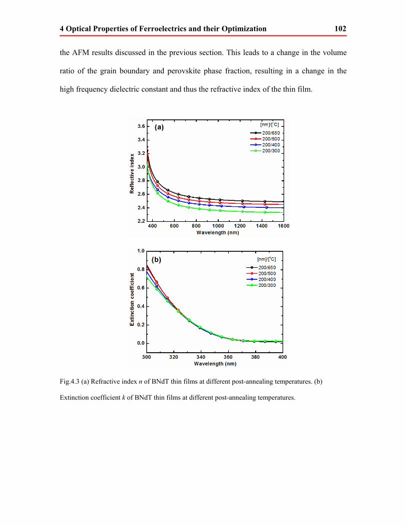
4 Optical Properties of Ferroelectrics and their Optimization 102
the AFM results discussed in the previous section. This leads to a change in the volume
ratio of the grain boundary and perovskite phase fraction, resulting in a change in the
high frequency dielectric constant and thus the refractive index of the thin film.
Fig.4.3 (a) Refractive index n of BNdT thin films at different post-annealing temperatures. (b)
Extinction coefficient k of BNdT thin films at different post-annealing temperatures.
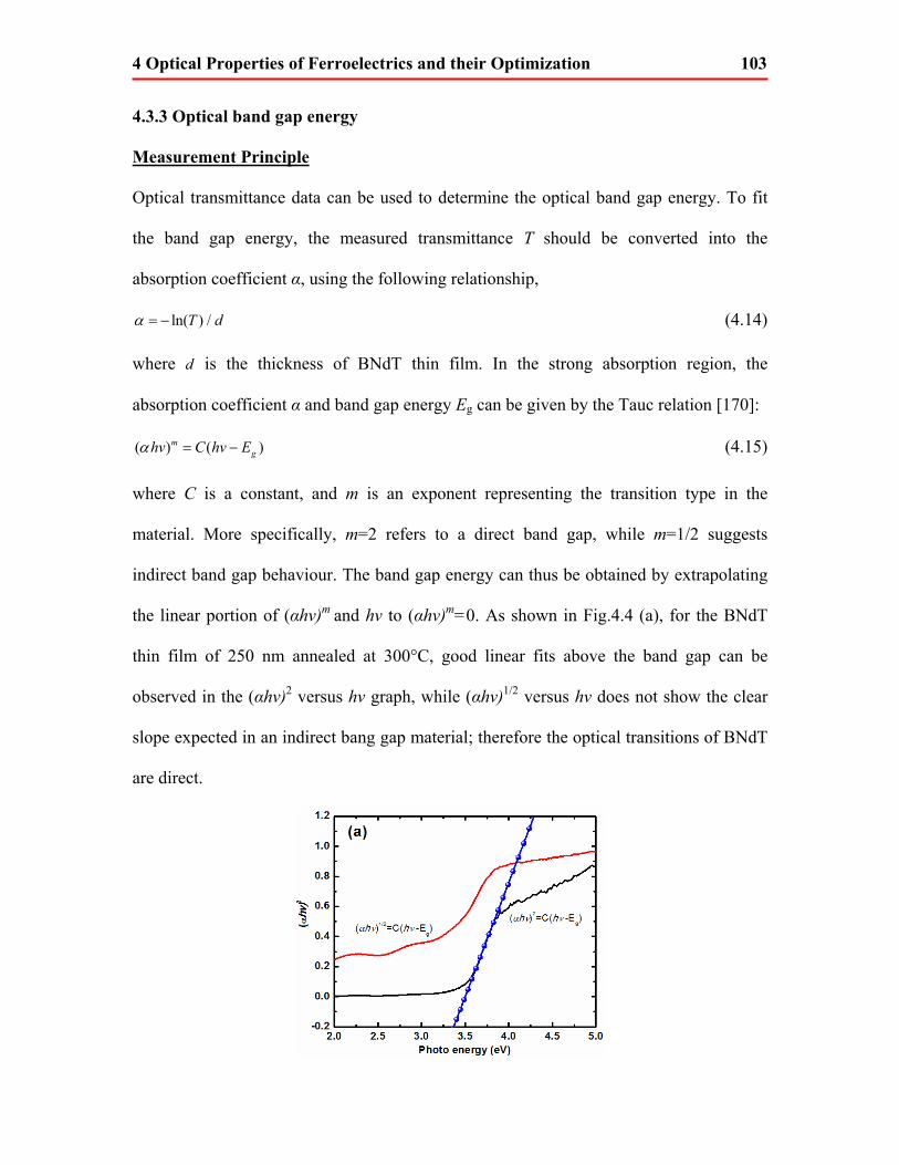
4 Optical Properties of Ferroelectrics and their Optimization 103
4.3.3 Optical band gap energy
Measurement Principle
Optical transmittance data can be used to determine the optical band gap energy. To fit
the band gap energy, the measured transmittance T should be converted into the
absorption coefficient α, using the following relationship,
ln( ) /T dα = − (4.14)
where is the thickness of BNdT thin film. In the strong absorption region, the
absorption coefficient α and band gap energy Eg can be given by the Tauc relation [170]:
d
( ) (m )ghv C hv Eα = − (4.15)
where C is a constant, and m is an exponent representing the transition type in the
material. More specifically, m=2 refers to a direct band gap, while m=1/2 suggests
indirect band gap behaviour. The band gap energy can thus be obtained by extrapolating
the linear portion of (αhν)m and hν to (αhν)m=0. As shown in Fig.4.4 (a), for the BNdT
thin film of 250 nm annealed at 300°C, good linear fits above the band gap can be
observed in the (αhν)2 versus hv graph, while (αhν)1/2 versus hv does not show the clear
slope expected in an indirect bang gap material; therefore the optical transitions of BNdT
are direct.

4 Optical Properties of Ferroelectrics and their Optimization 104
Fig4.4 (a) Optical absorption coefficient vs. photon energy of BNdT thin film (250 nm) processed at
300°C (b) Band gap energy of BNdT thin films (250 nm) at post annealing temperatures from 300°C
to 650°C.
Fig.4.4 (b) shows the band gap energy Eg values of the BNdT thin films (250 nm)
processed at different annealing temperatures from 300°C to 650°C, indicating a
modulation effect of the band gap energy during the fabrication process. It can be seen
that, in the 250 nm thick samples, Eg values drop from 3.42 to 3.02 eV as the post
annealing temperature increases from 300°C to 650°C. This variation agrees with the
results of traditional ferroelectric material PZT reported in the literature [171,172]. As
indicated in these papers, amorphous thin films exhibit larger Eg values compared to
polycrystalline films. In the lower temperature annealed samples, more amorphous
material is remanent, leading to larger free carrier concentrations and more potential
barriers across the boundaries, yielding larger internal electric fields and thus increasing
the optical band gap.
4 Optical Properties of Ferroelectrics and their Optimization 105
4.4 Quantum scale
In this section, Bi3.15Nd0.85Ti3O12 thin films with thicknesses from 50 to 100 nm are
processed at a crystallization temperature of 650°C, and different optical properties such
as the optical transmittance spectrum T(λ) and optical band gap Eg, are characterized to
investigate the importance of quantum scale in determining the optical performance of
the BNdT ferroelectric thin film.
4.4.1 Optical transmittance
Fig.4.5 shows the optical transmission spectra of the BNdT samples at UV-Vis-NIR
wavelengths from 200 to 2000 nm. There are three transmission spectra for BNdT thin
films with thicknesses of 50, 100, and 200 nm, post-annealed at 650°C. It can be seen
from Fig.4.5 (a) that the optical transmittance at 1550 nm does not show obvious
differences with increasing of thin film thickness, indicating that compared with the
obvious impact provided by the crystallization temperature, quantum scale does not play
an important role in determining the optical transmittance of the BNdT ferroelectric thin
film. However, an optical absorption edge blue shift is observed by decreasing the film
thickness, which is in agreement with the result reported in traditional ferroelectric PZT
materials [165], indicating an increase in the band gap energy. This effect will be
discussed in the upcoming section.
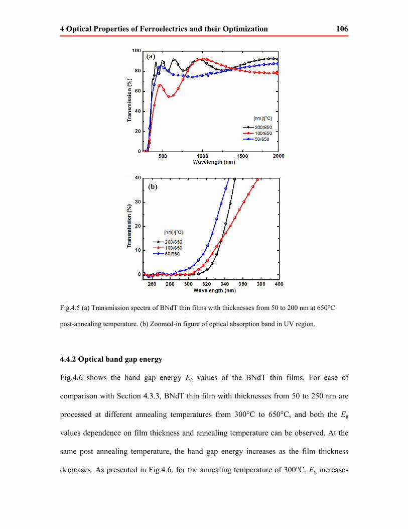
4 Optical Properties of Ferroelectrics and their Optimization 106
Fig.4.5 (a) Transmission spectra of BNdT thin films with thicknesses from 50 to 200 nm at 650°C
post-annealing temperature. (b) Zoomed-in figure of optical absorption band in UV region.
4.4.2 Optical band gap energy
Fig.4.6 shows the band gap energy Eg values of the BNdT thin films. For ease of
comparison with Section 4.3.3, BNdT thin film with thicknesses from 50 to 250 nm are
processed at different annealing temperatures from 300°C to 650°C, and both the Eg
values dependence on film thickness and annealing temperature can be observed. At the
same post annealing temperature, the band gap energy increases as the film thickness
decreases. As presented in Fig.4.6, for the annealing temperature of 300°C, Eg increases

4 Optical Properties of Ferroelectrics and their Optimization 107
from 3.42 to 3.76 eV as the thickness decreases from 250 to 50 nm. This is similar to the
results reported by D. Bao et al. [160], in which the measured optical band gap energy in
SrTiO3 thin layers is larger than in thick layers. The quantum-size effect in
semiconducting thin films can explain this phenomenon. When the thickness decreases,
the crystallite dimension also decreases, separating the inner atoms and reducing the unit
cell volume by means of increased residual compression stress. The grain boundaries and
imperfections are increased during this process. Such quantum-size effect, caused by the
thin film thickness scaling down, will eventually impact the optical performance of the
thin film and increase the optical band gap energy.
Fig.4.6 Band gap energy of BNdT thin films with thicknesses from 50 to 250 nm at post annealing
temperatures from 300°C to 650°C.
4.5 Ingredient substitution
In this section, we prepare Bi4-xNdxTi3O12 (x=0, 0.25, 0.5, and 0.85) material with
different Nd contents and report on how the Nd content affects the optical properties of
4 Optical Properties of Ferroelectrics and their Optimization 108
the Bi4-xNdxTi3O12 material. It will be seen that, as with annealing temperature, different
ingredient substitutions also exhibit considerable impact on the material’s optical
properties. Due to the ingredient change, some of the Bi4-xNdxTi3O12 material with a
thickness of 200 nm exhibits mild cracking during the annealing process. In order
maintain the same comparison criteria, we change the fabrication condition to ensure the
flatness and uniformity of the films utilized in the experiment. We increase all the Bi4-
xNdxTi3O12 films to 500 nm thickness, change the excess amount of bismuth titanate from
10% to 5%, and replace the crystallization annealing process with a RTA process at
600°C for 10 minutes in an air atmosphere. With this change, we finally obtained clear
and uniform BNdT thin films.
4.5.1 Optical transmittance
The measured optical transmittance spectra T(λ) of Bi4-xNdxT3O12 (x=0, 0.25, 0.5, and
0.85) thin films (500 nm in thickness) at wavelengths from 300 to 800 nm are presented
in Fig.4.7 (a). It can be seen that all BNdT thin films exhibit a transmittance of >50% in
the region from 600 to 800 nm, indicating a relatively weak optical absorption. The films
also exhibit a weak transparency of <10% with wavelengths less than 350 nm due to the
UV absorption in this region. The absorption edge can be observed around 330 nm. The
oscillatory manner of the transmittance curves indicates that a uniform and flat surface
topography of the BNdT thin films has been achieved.
Nd content plays a critical role in determining the optical transmittance properties of
BNdT thin films. It can be concluded that the BNdT thin film’s transmittance decreases
from 63% to 43%, at a wavelength of 600 nm, as the Nd content increases from 0 to 0.85.

4 Optical Properties of Ferroelectrics and their Optimization 109
This phenomenon can be attributed to the crystallinity variation with Nd substitution. In
the previous section, explained by Raman analysis, crystallinity decreases with the
increase in Nd substitution content. Since the transmittance of ferroelectric thin films can
be reduced by a degraded crystallinity quality [163], less optical transparency will be
observed under an increase in Nd substitution. Another contributing reason is the
substitution induced stress relaxation process. Due to the radius differences in Nd and Bi
atoms, the lattice constant will vary with increasing Nd content, resulting in an
amplification of the lattice distortion, and thus a larger stress relaxation in the
crystallization process and a corresponding change in the optical properties of the thin
film. Meanwhile, the optical absorption edge shift can be observed by changing the Nd
content, as shown in Fig.4.7(b), implying that a band gap energy variation also exists
upon Nd substitution, which will be investigated in the coming section.
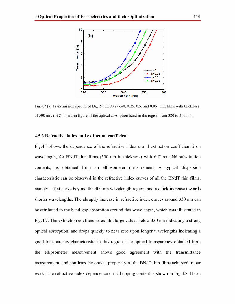
4 Optical Properties of Ferroelectrics and their Optimization 110
Fig.4.7 (a) Transmission spectra of Bi4-xNdxTi3O12 (x=0, 0.25, 0.5, and 0.85) thin films with thickness
of 500 nm. (b) Zoomed-in figure of the optical absorption band in the region from 320 to 360 nm.
4.5.2 Refractive index and extinction coefficient
Fig.4.8 shows the dependence of the refractive index n and extinction coefficient k on
wavelength, for BNdT thin films (500 nm in thickness) with different Nd substitution
contents, as obtained from an ellipsometer measurement. A typical dispersion
characteristic can be observed in the refractive index curves of all the BNdT thin films,
namely, a flat curve beyond the 400 nm wavelength region, and a quick increase towards
shorter wavelengths. The abruptly increase in refractive index curves around 330 nm can
be attributed to the band gap absorption around this wavelength, which was illustrated in
Fig.4.7. The extinction coefficients exhibit large values below 330 nm indicating a strong
optical absorption, and drops quickly to near zero upon longer wavelengths indicating a
good transparency characteristic in this region. The optical transparency obtained from
the ellipsometer measurement shows good agreement with the transmittance
measurement, and confirms the optical properties of the BNdT thin films achieved in our
work. The refractive index dependence on Nd doping content is shown in Fig.4.8. It can

4 Optical Properties of Ferroelectrics and their Optimization 111
be seen that the refractive index decreases slightly with an increase in Nd content, from
2.48 at x=0 to 2.2 at x=0.85, at 800 nm wavelength. The mean grain size variation upon
Nd substitution can be also an important factor. As indicated in the AFM measurement,
the mean grain size of the BNdT crystal decreases with the increase of Nd doping content,
leading to a change in the perovskite phase fraction and the volume ratio of the grain
boundary, thus changing the high frequency dielectric constant of BNdT and the
measured refractive index correspondingly [173].
Fig.4.8 Refractive index and extinction coefficient of Bi4-xNdxTi3O12 (x=0, 0.25, 0.5, and 0.85) thin
films.
4.5.3 Optical band gap energy
The band gap energy of BNdT thin films is plotted as a function of Nd substitution
content in Fig.4.9. It can be seen that the band gap energy increases from 3.4 to 3.5 eV as
the Nd substitution content increases from x=0 to x=0.85. The lattice parameter variation
and crystal distortion during the doping process can be recognized as an important

4 Optical Properties of Ferroelectrics and their Optimization 112
contributing factor to the change in band gap energy. By increasing the Nd substitution
content in the BTO system, the lattice parameter varies and the crystal distortion
increases, as explained by XRD and Raman analysis, working together to impact the
crystallinity quality of the BNdT thin film achieved, and thus impacting the measured
band gap energy. In the weak doping region, the introduction of Nd atoms with larger
atomic weight compared to the Bi atoms will help increase the energy of the chemical
bond with oxygen atoms and thus increase the band gap energy. However, with the
increase of Nd doping concentration, the non-bridging oxygen ions will also increase.
Such non-bridging oxygen ions will possess less binding capacities with the excited
electrons compared with the bridging oxygen [174,175], resulting in a negative factor to
the band gap energy increase, and thus a decrease in growth rate following an Nd content
increase. Further, the Nd-O bonds may also be broken or dangled by the non-bridging
oxygen ions [174], leading to more crystal distortion in the BNdT thin film.
Fig.4.9 Band gap energy variation with Nd substitution contents from 0 to 0.85 eV.

4 Optical Properties of Ferroelectrics and their Optimization 113
4.6 Conclusion
In this chapter, several optical parameters such as transmittance T, refractive index n,
extinction coefficient k, and optical band gap energy Eg, of the BNdT ferroelectric thin
film were investigated in detail. We started with the BNdT optical properties variation
due to crystallization temperature, demonstrating that different annealing temperatures
will impact the amorphous percentage and stress relaxation process, and thus change the
optical performance of the BNdT material. Then, the quantum scale effect was examined
and found to be responsible for changes in the unit cell volume and grain boundaries,
variations that have an impact on the optical performance of the BNdT material. Finally,
the ingredient substitution effect was examined. It was concluded that different Nd
substitution concentrations could change the crystallization distortion of Bi4-xNdxT3O12
materials, and modulate the optical parameters. Our study presented the first systematic
experimental study on this subject and demonstrated well-defined optical properties of
the BNdT material. Moreover, the study presented here, on different impact mechanisms,
provides us with more freedom to optimize the optical performance of BNdT.

4 Optical Properties of Ferroelectrics and their Optimization 114
5 Multiferroic and Optimization 115
Chapter 5
Multiferroic and Optimization
M 5.1 Introduction
ultiferroelectrics are defined as materials that possess two or more
primary ferroic properties, namely, ferroelectricity, ferromagnetism,
and ferroelasticity, simultaneously in the same phase [176-178]. In
particular, those that possess a coupling between the ferroelectric and magnetic orderings
have attracted widespread attention due to their potential in novel, technically demanding
applications. The coexistence of ferroelectricity and magnetism offers more freedom of
control in new devices based on magnetic and electric fields mutual effects [3,179].
Recently, the lead-free multiferroelectric material BiFeO3 (BFO), with a rhombohedrally
distorted pervoskite structure in the space group R3c [180], has been considered a
promising candidate in room temperature magnetoelectric applications due to its high
Curie temperature (~850°C) [181] and high Neel temperature (~370°C) [182]. Moreover,
a high paraelectric-to-ferroelectric transition temperature suggests that BFO has the
potential to exhibit a very large spontaneous polarization (Ps) [80]. As reported by Wang,
et al. [3], BFO thin films achieved by pulsed laser deposition (PLD) exhibit a remanent
5 Multiferroic and Optimization 116
polarization (Pr) of 100 μC/cm2, and other chemical solution deposition (CSD) derived
BFO thin films also exhibit good polarization performance [183].
However, it is difficult to characterize ferroelectric properties at room temperature
because the BFO material has low resistivity, which prevents it from exhibiting
maximum polarization performance [80,81]. The low resistivity can be attributed to the
Fe ions (Fe3+ and Fe2+) valence fluctuation, Bi atoms volatile nature, oxygen vacancies,
and impurity phases [41,79]. In this chapter, we examine different attempts to optimize
the ferroelectric properties of the BFO material, and demonstrate successful room
temperature characterization of it.
The remainder of this chapter is organized as follows. Section 5.2 introduces two
different optimization approaches used in this experiment and describes the physical
nature of these two methods. Starting from Section 5.3, we focus on the first optimization
routine, namely, the multilayer methodology. Fabrication technology, structural analysis,
ferroelectric characterization, and dielectric examination are described in detail in
Sections 5.3 to 5.6. In the latter part of this chapter, we move on to discuss another
optimization approach, namely, dual-site substitution technology, and we process the
corresponding characterization. From Sections 5.7 to 5.9, a detailed characterization of
dual-site substituted BFO materials is provided experimentally and theoretically. This
chapter is summarized and concluded in Section 5.10.
5.2 Different optimization approaches
To reduce the conductivity of BFO, three different routines have been investigated and
reported in the literature, namely, a single phase BFO compound [82], a formation of a

5 Multiferroic and Optimization 117
solid solution with other ABO3 pervoskite materials [83], and ion atoms substitution at Bi
and Fe sites in the BFO crystal [84]. However, the first two methods have intrinsic
disadvantages that prevent their further application in the multiferroic field. In the single
phase BFO, leakage paths are dramatically reduced due to the improvement in
ferroelectric phase, and the ferroelectric hysteresis loop can be measured by deducing the
conductivity. However, single phase BFO can only be achieved by molecular beam
epitaxy (MBE). MBE is an expensive fabrication technology and the growth rate is fairly
low, preventing it from meeting large-scale production demands. The solid solution
approach mixes BFO and other ABO3 perovskite materials, such as BaTiO3,
PbFe0.5Nb0.5O3, PZT, PbTiO3, PrFeO3, and DyFeO3 [184-187]. The similar crystal
structure promotes the crystallization process of the BFO material and helps to induce a
relatively well-defined pseudo single crystal phase in the BFO material. However, the
high operational temperature in the process is not compatible with existing silicon-based
technology and prevents the integration of BFO into current silicon-based memory
applications. Moreover, the addition of different ABO3 materials introduces impurities
and results in a transition phase in the fabrication process. Among the three routines, ion
atoms substitution is the most effective technology in reducing the conductivity of BFO.
Numerous doping elements were introduced into BFO, and rare-earth ions such as La, Nd,
and so on, are considered to be the most successful attempted thus far due to their control
over the volatile nature of Bi and the suppression of oxygen vacancies [41].
In this study, we initiate an innovative multilayer technology by introducing a seeding
layer between the BFO ferroelectric and the silicon substrate. With this seeding layer, the
crystallization process of the upper BFO material can be induced, resulting in a better

5 Multiferroic and Optimization 118
degree of crystallinity and lower leakage properties. Meanwhile, we improve the existing
ion atoms substitution technology and demonstrate a Bi and Fe dual-site substitution in
the optimization of BFO ferroelectric properties.
5.2.1 Multilayer technology
Multilayer technology is quite mature in thin film fabrication and characterization. By
depositing different thin film materials on the substrate, the as-prepared multilayer can
exhibit different properties compared to films of any other composition. During the
deposition process, different layers impact each other and change the structural and thus
the functional properties of the entire multilayer. In this multi-inducing process, the lower
layer, known as the seeding layer, plays an important role in the crystallization process of
the upper layer. During all thin film deposition processes, the nucleation and
crystallization process is highly determined by the substrate; the same fabrication recipe
will result in completely different material crystallizations with different substrates. In
multilayer technology, the seeding layer is carefully selected and only materials with the
same crystal type, similar lattice parameters, and compatible fabrication conditions will
be considered. An appropriate seeding layer will improve and induce the crystallization
process of the upper layer and dramatically improve the functional properties in an
application [188]. In our experiment, BNdT thin film, discussed in Chapters 3 and 4, is
used as the seeding layer of the BFO material. The well-defined ferroelectric properties
and similar lattice parameters make BNdT a promising option for the seeding layer in this
multilayer structure.
5 Multiferroic and Optimization 119
5.2.2 Rare-earth ions substitution
As with multilayer technology, rare earth substitution also aims to improve the electrical
resistivity of the BFO material and thus improve the room temperature application
performance. As explained at the beginning of this chapter, the relatively low electric
resistivity of BFO is attributed to the valence fluctuation of Fe ions (Fe3+ to Fe2+), which
requires oxygen vacancies for charge compensation and produces electron hopping in
films. The oxidation state of Fe greatly depends on the processing conditions and the type
and amount of dopants [79]. In order to improve the polarization properties of BFO at
room temperature, the site-engineering concept has been proposed. There has been much
research done on enhancing the room temperature ferroelectric properties of the BFO thin
film with rare earth and other ions substitution. For example, Bi-site substitution with La
and Nd atoms for controlling volatile Bi atoms and suppressing generation of oxygen
vacancies has been attempted in BFO thin films [40,41]; as well, Fe-sited substitutions
such as Nb and Mn atoms have been reported by S. K. Singh and C. F. Chung, et al. to
fill oxygen vacancies in bulk ceramics [39,42,43]. However, most of the reports to date
focus on single-site substitution (Bi-sited or Fe-sited), and less attention has been devoted
to Bi and Fe dual-site substitution in the optimization of BFO ferroelectric properties. In
this chapter, we report the Bi and Fe dual-site substituted BFO crystal with La, Nd, Nb,
and Mn. The structural, ferroelectric, and electrical properties of different substituted
BFO materials will be investigated and compared. An optimized substitution pattern that
can be applied in BFO-based electrical and magnetic applications is obtained from this
study.
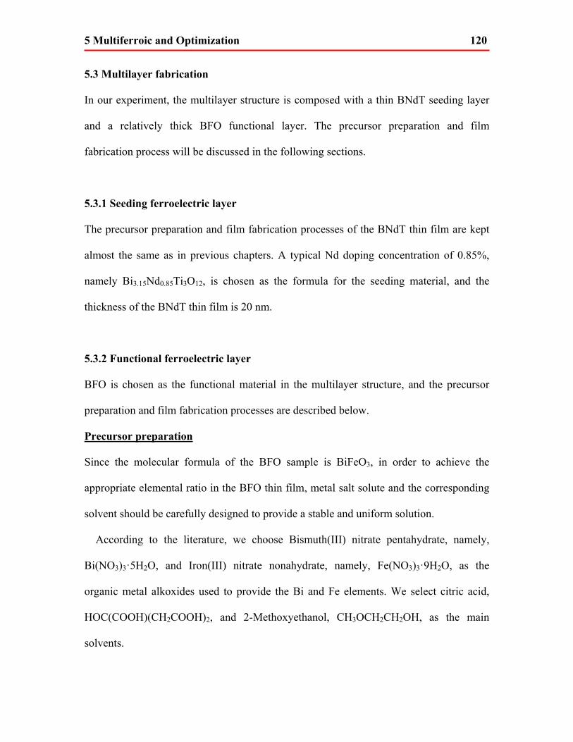
5 Multiferroic and Optimization 120
5.3 Multilayer fabrication
In our experiment, the multilayer structure is composed with a thin BNdT seeding layer
and a relatively thick BFO functional layer. The precursor preparation and film
fabrication process will be discussed in the following sections.
5.3.1 Seeding ferroelectric layer
The precursor preparation and film fabrication processes of the BNdT thin film are kept
almost the same as in previous chapters. A typical Nd doping concentration of 0.85%,
namely Bi3.15Nd0.85Ti3O12, is chosen as the formula for the seeding material, and the
thickness of the BNdT thin film is 20 nm.
5.3.2 Functional ferroelectric layer
BFO is chosen as the functional material in the multilayer structure, and the precursor
preparation and film fabrication processes are described below.
Precursor preparation
Since the molecular formula of the BFO sample is BiFeO3, in order to achieve the
appropriate elemental ratio in the BFO thin film, metal salt solute and the corresponding
solvent should be carefully designed to provide a stable and uniform solution.
According to the literature, we choose Bismuth(III) nitrate pentahydrate, namely,
Bi(NO3)3·5H2O, and Iron(III) nitrate nonahydrate, namely, Fe(NO3)3·9H2O, as the
organic metal alkoxides used to provide the Bi and Fe elements. We select citric acid,
HOC(COOH)(CH2COOH)2, and 2-Methoxyethanol, CH3OCH2CH2OH, as the main
solvents.

5 Multiferroic and Optimization 121
Precursor list
All chemicals are provided by Sigma-Aldrich.
Table.5.1 Chemicals used to prepare the BFO precursor.
Precursor preparation recipe
In order to maintain the mol ratio of Bi and Fe at 1:1, the mass of both the metal salts are
calculated as,
M[Bi(NO3)3·5H2O]= 0.025 0.2 485.07 (1 10%)98%
× × × += 2.722 g
M[Fe(NO3)3·9H2O]= 0.025 0.2 404.00 198%
× × ×=2.061 g
A detailed precursor preparation process is described as follows.
(1) 2.722 g Bi(NO3)3·5H2O and 2.061 g Fe(NO3)3·9H2O are both dissolved in
CH3OCH2CH2OH for a total volume of 50 ml. Excess bismuth nitrate of 10% is added to
compensate for the Bi loss during the thermal annealing process. The mixed solution is
stirred for 10 hrs.
(2) 1.584 g HOC(COOH)(CH2COOH)2 is then added as the deducing agent.
(3) The as-prepared precursor is stirred at 500 rpm for 10 hrs and left to stand for 24
hrs at room temperature.
5 Multiferroic and Optimization 122
(4) The as prepared solution is filtered using a 0.2 μm filter and stored in a conical
beaker.
A photograph of the as-prepared BFO solution is shown in Fig 5.1; it can be seen that a
uniform and stable solution is achieved in our experiment.
Fig.5.1 A photograph of the as-prepared BFO solution.
BFO thin film fabrication
The fabrication process of the BFO ferroelectric thin film can be summarized as follows.
(1) Spin coating deposition. The as-prepared BNdT thin film is introduced as the
substrate and the BFO thin film is deposited on top of the substrate. The spin rate is 2000
rpm, lasting for 1.5 min each time. This process is repeated until the desired thickness
(200 nm) of the BFO thin film is obtained.
(2) Pyrogenation. The as-prepared BFO thin film is subject to a pyrogenation process
at 550°C for 30 s in air, in order to help the organic solvent volatilize and the ferroelectric
crystallize.

5 Multiferroic and Optimization 123
(3) Pre-crystallization annealing. The BFO thin film is then introduced to a RTA
process in oxygen atmosphere. The temperature quickly rises from room temperature to
200°C, at which it is kept for 20 s, followed by an increase up to 550°C in 3.9 s (heating
rate: 90 °C/s), lasting for 60 s.
(4) Crystallization annealing. After processes (1) to (3) are repeated an appropriate
number of times, a crystallization annealing process of 550°C for 10 min in air is applied
to the as-prepared BFO thin films.
(5) Top electrode sputtering. Top Pt electrodes are introduced by means of a DC
magnetron sputtering with a shadow mask. The diameter of the top electrode is 200 μm.
A schematic illustration of the as-prepared BFO/BNdT multilayer structure is
demonstrated in Fig.5.2. For comparison purposes, different multilayer structures are
fabricated and investigated. It can be concluded that different multilayer structures will
display completely different performance, and that the seeding layer plays an important
role in determining the ferroelectric properties of the upper BFO ferroelectric layer [188].
Fig.5.2 (a) Multilayer structure of Pt/BFO(200 nm)/BNdT(20 nm)/Pt, (b) Multilayer structure of
Pt/BNdT(20 nm)/BFO(200 nm)/Pt, (c) Pt/BFO(200 nm)/Pt, and (d) Pt/BNdT(20 nm)/Pt.

5 Multiferroic and Optimization 124
5.4 Multilayer structural characterization
5.4.1 X-ray diffraction analysis
Fig.5.3 shows the XRD patterns of the BFO(200 nm)/BNdT(20 nm) multilayer,
BNdT(200 nm), and BFO(200 nm) thin films. It is easy to index all of the diffraction
peaks of the BFO and BNdT thin films achieved. In the Pt/BFO/Pt and Pt/BNdT/Pt
structures, it is found that both the BFO and BNdT thin films achieve a good perovskite
structure without any secondary phases. The BFO thin film exhibits a high (110)
orientation, which is consistent with the result reported by J. G. Wan, et al. [189]. The
diffraction peaks of BNdT reveal high c-axis orientation with few random oriented peaks
(117), indicating good ferroelectric properties, as reported by Chon, et al. [34]. In the
BFO/BNdT/Pt multilayer, BNdT still exhibits high c-axis orientation, such as (004),
(006), (008), indicating that the upper BFO layer and post fabrication process does not
impact the crystallization process of the BFO material. Notably, the BFO thin film is seen
to have a high (110) preferred orientation and a relatively high degree of 42% (111)
preferred orientation in the multilayer structure. It is also seen that the BNdT seeding
layer helps enhance the growth of (111) preferred BFO grains. Coupling reactions should
occur between the two ferroelectric materials, and the BNdT layer induces the
crystallization and growth of the upper BFO film. As reported in the literature, the
spontaneous polarization of BFO is along [111]; therefore such (111) preferred
orientation BFO in the multilayer should provide better ferroelectric properties [190].
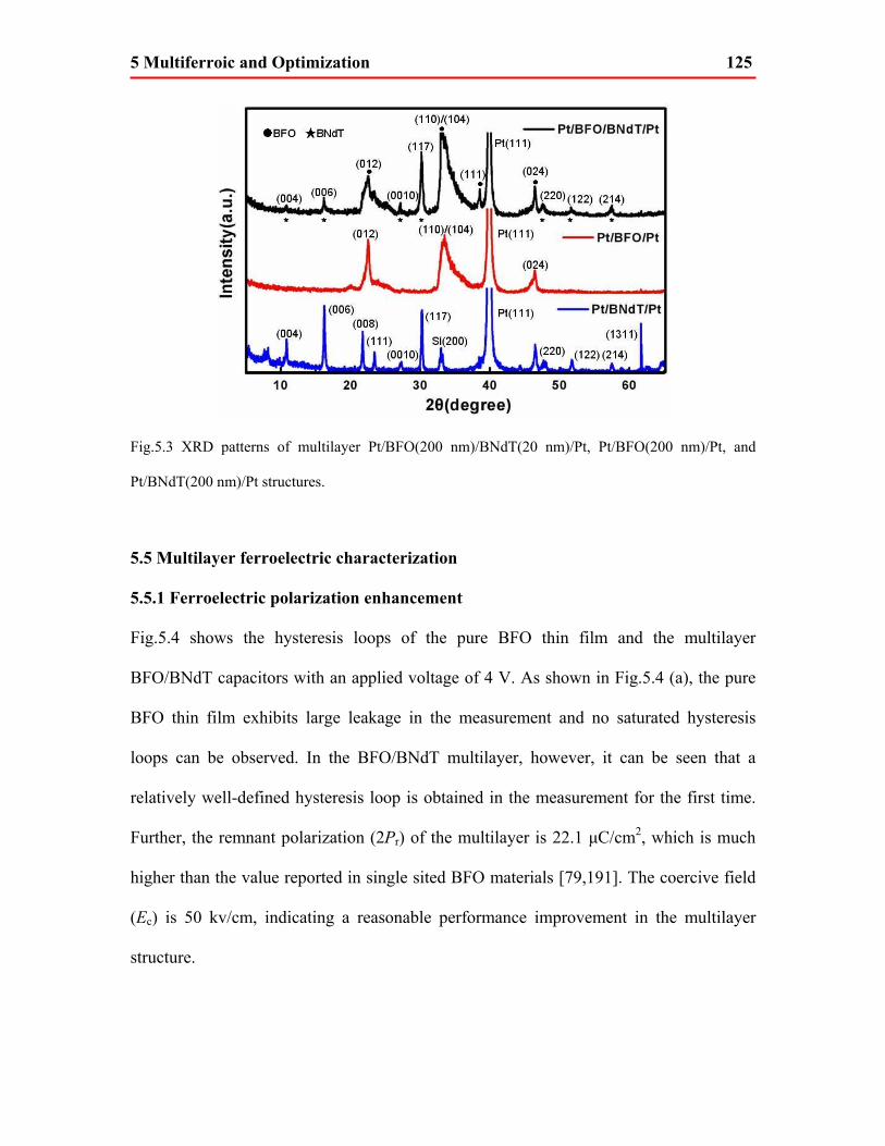
5 Multiferroic and Optimization 125
Fig.5.3 XRD patterns of multilayer Pt/BFO(200 nm)/BNdT(20 nm)/Pt, Pt/BFO(200 nm)/Pt, and
Pt/BNdT(200 nm)/Pt structures.
5.5 Multilayer ferroelectric characterization
5.5.1 Ferroelectric polarization enhancement
Fig.5.4 shows the hysteresis loops of the pure BFO thin film and the multilayer
BFO/BNdT capacitors with an applied voltage of 4 V. As shown in Fig.5.4 (a), the pure
BFO thin film exhibits large leakage in the measurement and no saturated hysteresis
loops can be observed. In the BFO/BNdT multilayer, however, it can be seen that a
relatively well-defined hysteresis loop is obtained in the measurement for the first time.
Further, the remnant polarization (2Pr) of the multilayer is 22.1 μC/cm2, which is much
higher than the value reported in single sited BFO materials [79,191]. The coercive field
(Ec) is 50 kv/cm, indicating a reasonable performance improvement in the multilayer
structure.

5 Multiferroic and Optimization 126
Fig.5.4 Ferroelectric hysteresis loops of (a) Pt/BFO(200 nm)/Pt, and (b) Pt/BFO(200 nm)/BNdT(20
nm)/Pt capacitors.
The enhancement in ferroelectric properties of the multilayer may be attributed to two
different factors [188]. One potential reason is the coupling reaction between the two thin
films, which causes an enhancement in the crystallization process and thus in the
ferroelectric properties of the BFO film. Another possible reason is that it is the BNdT
layer with 20 nm thickness that exhibits the excellent remnant polarization, rather than
the multilayer. However, the BNdT (20 nm) sample exhibited poor remnant polarization
in the measurement. The remnant polarization was about 1.2μC/cm2, as shown in Fig. 5.5
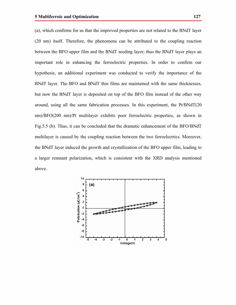
5 Multiferroic and Optimization 127
(a), which confirms for us that the improved properties are not related to the BNdT layer
(20 nm) itself. Therefore, the phenomena can be attributed to the coupling reaction
between the BFO upper film and the BNdT seeding layer; thus the BNdT layer plays an
important role in enhancing the ferroelectric properties. In order to confirm our
hypothesis, an additional experiment was conducted to verify the importance of the
BNdT layer. The BFO and BNdT thin films are maintained with the same thicknesses,
but now the BNdT layer is deposited on top of the BFO film instead of the other way
around, using all the same fabrication processes. In this experiment, the Pt/BNdT(20
nm)/BFO(200 nm)/Pt multilayer exhibits poor ferroelectric properties, as shown in
Fig.5.5 (b). Thus, it can be concluded that the dramatic enhancement of the BFO/BNdT
multilayer is caused by the coupling reaction between the two ferroelectrics. Moreover,
the BNdT layer induced the growth and crystallization of the BFO upper film, leading to
a larger remnant polarization, which is consistent with the XRD analysis mentioned
above.

5 Multiferroic and Optimization 128
Fig.5.5 Ferroelectric hysteresis loops of (a) Pt/BNdT(20 nm)/Pt, and (b) Pt/BNdT(20 nm)/BFO(200
nm)/Pt capacitors.
5.5.2 Fatigue properties enhancement
We perform ferroelectric fatigue tests by applying pulses of 1 MHz to the multilayer
capacitors. Fig.5.6 (a) shows the normalized polarization as a function of polarization
switching cycles; as well, the hysteresis loop before and after the fatigue test is shown in
Fig.5.6 (b). The multilayer exhibits good fatigue properties, and it demonstrates little
fatigue degradation (<5%) upon 1×10¹⁰ switching cycles at an applied voltage of 4 V,
with little degradation observed in the two hysteresis loops. As reported by J. Wang, et al.
[3], BFO is very sensitive to small changes in lattice parameters; also the origin of the
good fatigue resistance may be attributed to the coupling between the two ferroelectric
layers. Therefore, the BNdT layer induces the crystallization of the BFO film, affecting
the lattice parameters of the BFO film, leading to a good fatigue resistance.

5 Multiferroic and Optimization 129
Fig.5.6 (a) Fatigue curves of normalized polarization as a function of number of switching cycles at
4V. (b) Ferroelectric hysteresis loop before and after the fatigue test.
5.5.3 CV/IV properties enhancement
CV investigation is an important topic in the study of ferroelectrics. Due to the unique
memory characteristics of ferroelectrics, a ferroelectric capacitor exhibits a different CV
pattern compared with that of traditional MOS capacitors. In common ferroelectrics-
based memory devices, the CV patterns can be classified as MFM (Metal-Ferroelectric-
Metal) type or MFS (Metal-Ferroelectric-Semiconductor) type. In the MFM type, a
butterfly-shaped CV curve can be observed in the measurement. The symmetry of the CV
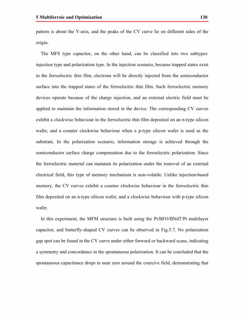
5 Multiferroic and Optimization 130
pattern is about the Y-axis, and the peaks of the CV curve lie on different sides of the
origin.
The MFS type capacitor, on the other hand, can be classified into two subtypes:
injection type and polarization type. In the injection scenario, because trapped states exist
in the ferroelectric thin film, electrons will be directly injected from the semiconductor
surface into the trapped states of the ferroelectric thin film. Such ferroelectric memory
devices operate because of the charge injection, and an external electric field must be
applied to maintain the information stored in the device. The corresponding CV curves
exhibit a clockwise behaviour in the ferroelectric thin film deposited on an n-type silicon
wafer, and a counter clockwise behaviour when a p-type silicon wafer is used as the
substrate. In the polarization scenario, information storage is achieved through the
semiconductor surface charge compensation due to the ferroelectric polarization. Since
the ferroelectric material can maintain its polarization under the removal of an external
electrical field, this type of memory mechanism is non-volatile. Unlike injection-based
memory, the CV curves exhibit a counter clockwise behaviour in the ferroelectric thin
film deposited on an n-type silicon wafer, and a clockwise behaviour with p-type silicon
wafer.
In this experiment, the MFM structure is built using the Pt/BFO/BNdT/Pt multilayer
capacitor, and butterfly-shaped CV curves can be observed in Fig.5.7. No polarization
gap spot can be found in the CV curve under either forward or backward scans, indicating
a symmetry and concordance in the spontaneous polarization. It can be concluded that the
spontaneous capacitance drops to near zero around the coercive field, demonstrating that

5 Multiferroic and Optimization 131
the BFO/BNdT multilayer exhibits a random electric domain orientation and a high
domain energy density.
Fig.5.7 CV curves of the Pt/BFO/BNdT/Pt multilayer capacitor.
Fig.5.8 shows the J-V curves of the Pt/BFO/BNdT/Pt multilayer capacitor, and a
leakage density of 2×10⁻⁹ A/cm-2 with an applied voltage of 2 V is observed in the
multilayer. Compared to the 3×10⁻⁷ A/cm-2 leakage density of the Pt/BNdT/Pt capacitor,
an improvement of nearly two orders of magnitude in J-V curves is obtained with the
Pt/BFO/BNdT/Pt multilayer structure. The BNdT seeding layer induces the
crystallization process of the BFO upper layer, and improves the degree of crystallization
in the multilayer. A well-defined perovskite structure with less leakage paths will be
desirable in many ferroelectric-based electrical applications.
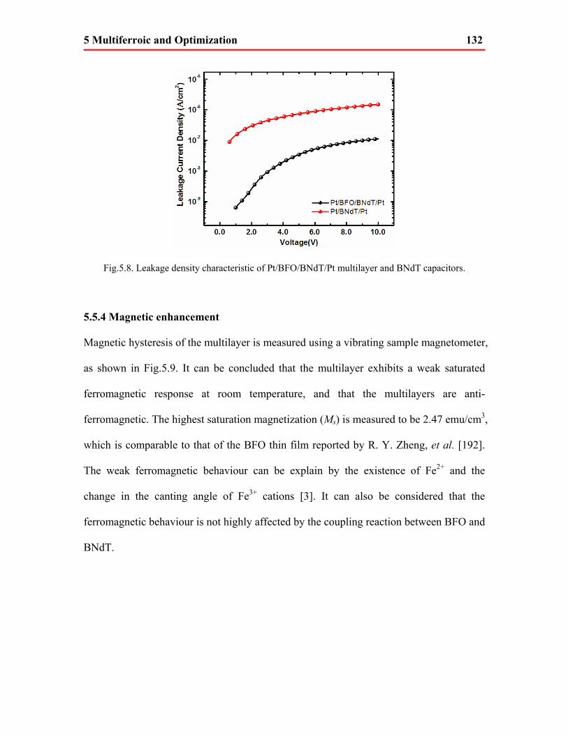
5 Multiferroic and Optimization 132
Fig.5.8. Leakage density characteristic of Pt/BFO/BNdT/Pt multilayer and BNdT capacitors.
5.5.4 Magnetic enhancement
Magnetic hysteresis of the multilayer is measured using a vibrating sample magnetometer,
as shown in Fig.5.9. It can be concluded that the multilayer exhibits a weak saturated
ferromagnetic response at room temperature, and that the multilayers are anti-
ferromagnetic. The highest saturation magnetization (Ms) is measured to be 2.47 emu/cm3,
which is comparable to that of the BFO thin film reported by R. Y. Zheng, et al. [192].
The weak ferromagnetic behaviour can be explain by the existence of Fe2+ and the
change in the canting angle of Fe3+ cations [3]. It can also be considered that the
ferromagnetic behaviour is not highly affected by the coupling reaction between BFO and
BNdT.
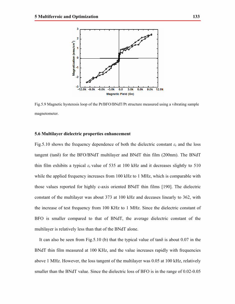
5 Multiferroic and Optimization 133
Fig.5.9 Magnetic hysteresis loop of the Pt/BFO/BNdT/Pt structure measured using a vibrating sample
magnetometer.
5.6 Multilayer dielectric properties enhancement
Fig.5.10 shows the frequency dependence of both the dielectric constant εr and the loss
tangent (tanδ) for the BFO/BNdT multilayer and BNdT thin film (200nm). The BNdT
thin film exhibits a typical εr value of 535 at 100 kHz and it decreases slightly to 510
while the applied frequency increases from 100 kHz to 1 MHz, which is comparable with
those values reported for highly c-axis oriented BNdT thin films [190]. The dielectric
constant of the multilayer was about 373 at 100 kHz and deceases linearly to 362, with
the increase of test frequency from 100 KHz to 1 MHz. Since the dielectric constant of
BFO is smaller compared to that of BNdT, the average dielectric constant of the
multilayer is relatively less than that of the BNdT alone.
It can also be seen from Fig.5.10 (b) that the typical value of tanδ is about 0.07 in the
BNdT thin film measured at 100 KHz, and the value increases rapidly with frequencies
above 1 MHz. However, the loss tangent of the multilayer was 0.05 at 100 kHz, relatively
smaller than the BNdT value. Since the dielectric loss of BFO is in the range of 0.02-0.05
5 Multiferroic and Optimization 134
[79], the result seems to be reasonable. Compared to the BNdT thin film, it can be
proposed that the BFO/BNdT multilayer may show better performance in high frequency
applications. This difference in dielectric properties may be attributed to the coupling
reaction between the two ferroelectrics, which adjusts the dielectric constant and
optimizes the dielectric loss.
Fig.5.10 (a) Dielectric constant of the multilayer as a function of frequency (b) Loss tangent of the
multilayer as a function of frequency.

5 Multiferroic and Optimization 135
5.7 Dual-site substitution fabrication
From this section on, we will discuss a different approach to improving the room
temperature ferroelectric properties of the BFO material, namely, using dual-site
substitution technology. Unlike the previous multilayer approach, where the aim was to
improve the degree of crystallization in the BFO material, dual-site substitution
technology intentionally introduces substitution atoms to the system and changes the
BFO crystal structure correspondingly. Substituted atoms with different atomic radii will
replace the Bi and Fe sites in the BFO crystal, distort the BFO crystal, and control the
volatile nature of Bi and the suppression of oxygen vacancies.
Rare earth elements La, Nd, Nb, and Mn are introduced as the substitution elements.
BFO crystals were substituted with 5 at. % ions (La, Nb, Nd, and Mn) with different
chemical compositions. The stoichiometric BFO, Bi0.95Nd0.05Fe0.95Nb0.05O3 (BNFNO),
Bi0.95Nd0.05Fe0.95Mn0.05O3 (BNFMO), and Bi0.95La0.05Fe0.95Nb0.05O3 (BLFNO) are used in
our experiment; the fabrication processes are the same as described in Section 5.3.2.
5.8 Dual-site substitution structural characterization
5.8.1 X-ray diffraction analysis
Fig.5.11 shows the X-ray diffraction patterns of the BFO, BNFNO, BNFMO, and
BLFNO thin films. It can be seen that all of the XRD peaks can be indexed using a
rhombohedral structure with some impurities and secondary phases. Merging and shifting
of the diffraction peaks in the doped BFO thin films can be observed, indicating a
structural transformation induced by substitution. In the pure BFO and BLFNO crystals,
the (100) peak exhibits relatively larger intensity compared with the BNFNO and

5 Multiferroic and Optimization 136
BNFMO samples; the cause of this effect is that the La and Nb substitutions help enhance
the crystallization of the BFO material in a c-axis preferred orientation. As found for the
BNFNO crystal, diffraction peaks (104) and (110) in pure BFO crystal emerge and shift
to a higher angle, describing a structural transformation. As reported in the literature, by
changing the substitution concentration, the BFO structure will change from
rhombohedral to tetragonal; this result is in agreement with what is seen in our
experiment. Furthermore, impurities and secondary phases can be suppressed by using
substitution. The intrinsic stability of La, Nd, Nb, and Mn atoms compared with the
volatile nature of Bi contributes to this phenomenon, indicating that refined
crystallization of BFO with less impurities and secondary phases can be achieved by
modulating different ion substitutions. Further, since the chemical bond strengths of La,
Nd, Nb, and Mn atoms with oxygen are not equal to that of the Bi-O bond, the
crystallization temperature will vary compared to pure BFO [193]. This difference in
bond strengths can be manipulated in order to study the substitution induced
crystallization temperature variation of the BFO material.
Fig.5.11. XRD patterns of BFO, BNFNO, BNFMO, and BLFNO thin films.

5 Multiferroic and Optimization 137
5.8.2 Raman scattering analysis
Raman scattering spectra of BFO, BNFNO, BNFMO, and BLFNO thin films are shown
in Fig.5.12. The peak position of each component, i.e., the natural frequency of each
Raman active phonon mode, can be obtained by fitting the measured spectra and
decomposing the fitted curves into individual Lorentzian components [193]. As reported
in the literature, the Raman active phonon modes of the rhombohedral R3c BFO crystal
can be given by the following irreducible representation Г=4A1+9E [194-196], where A1
modes can only be observed in parallel polarization, but E modes can be found in both
parallel and crossed polarizations [197]. As shown in Fig.5.12 (a), four A1 modes and
four E modes can be observed in our sol-gel derived BFO thin film. It can be seen that
there are A1-1, A1
-2, and A1-3 modes with strong scattering intensities located at 140, 170,
and 217 cm-1, respectively, and an A1-4 mode with relatively weak scattering intensity at
470 cm-1. These results are comparable with those reported for PLD derived single
crystalline BFO (A1-1, A1
-2, A1-3 and A1
-4, at 136, 168, 211, and 425 cm-1, respectively)
[194,195]. The slight difference in Raman peak positions between reported results and
our study is attributed to the oxygen stoichiometry and internal stress during the
fabrication process. Also, four E modes with medium scattering intensity can be indexed
at 90, 270, 368, and 539 cm-1.
The substitution induced Raman peak shift and suppression is also investigated, as
shown in Fig.5.12 (b). The Raman active phonon mode A1-3 (~217 cm-1) exhibits a
positive shift after ion substitution, which is consistent with the result reported by A.
Lahmar, et al. [198]. This scattering peak shift can be attributed to the stiffening of the A-
O bond induced by the substituted ions with different atomic radii, resulting in a change
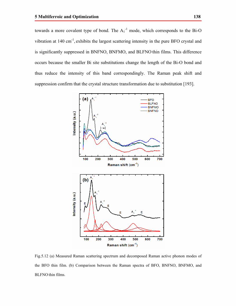
5 Multiferroic and Optimization 138
towards a more covalent type of bond. The A1-1 mode, which corresponds to the Bi-O
vibration at 140 cm-1, exhibits the largest scattering intensity in the pure BFO crystal and
is significantly suppressed in BNFNO, BNFMO, and BLFNO thin films. This difference
occurs because the smaller Bi site substitutions change the length of the Bi-O bond and
thus reduce the intensity of this band correspondingly. The Raman peak shift and
suppression confirm that the crystal structure transformation due to substitution [193].
Fig.5.12 (a) Measured Raman scattering spectrum and decomposed Raman active phonon modes of
the BFO thin film. (b) Comparison between the Raman spectra of BFO, BNFNO, BNFMO, and
BLFNO thin films.

5 Multiferroic and Optimization 139
5.8.3 Electron microscope analysis
AFM surface morphologies of BFO, BNFNO, BNFMO, and BLFNO thin films are each
examined and are shown in Fig.5.13 (a)-(d). Close-packed spherical grains and a smooth
and uniform surface can be found in all of the samples. It is concluded that ion
substitution plays a critical role in determining the grain size. The pure BFO exhibits a
mean grain size of ~150 nm, whereas in the BNFMO and BLFNO thin films the mean
grain size is reduced to ~50 nm. In the BNFNO crystal, the mean grain size is measured
to be ~10 nm, only one fifteenth of the value for the pure BFO crystal. Since the grain
size is a substantial contributing factor to the leakage properties, and crystals possessing
small grain sizes always exhibit lower leakage current density, the ion substitution will
help reduce the leakage current density and thus improve the ferroelectric properties
[193], as will be discussed in the coming section.

5 Multiferroic and Optimization 140

5 Multiferroic and Optimization 141
Fig.5.13 AFM surface topography of BFO (a), BNFMO (b), BNFNO (c), and BLFNO (d) thin films.
5.9 Dual-site substitution ferroelectric properties characterization
5.9.1 Remanent polarization
Fig.5.14 shows the P-E hysteresis loops of the BFO, BNFNO, BNFMO, and BLFNO thin
films. The pure BFO thin film exhibits a distorted hysteresis loop, indicating a large
leakage current density. By substituting ions, a small remanent polarization is observed in
the BNFNO, BNFMO, and BLFNO thin films, as shown in Fig.5.14 (b)-(d). It can be
seen that none of the hysteresis loops are saturated, suggesting that the required saturation
voltage of BNFNO, BNFMO, and BLFNO thin films is higher than the maximum output
that our equipment can offer. However, an obvious improvement in ferroelectric
properties can still be inferred from the P-E measurement, indicating the usefulness of
ion substitution.

5 Multiferroic and Optimization 142
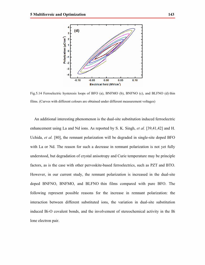
5 Multiferroic and Optimization 143
Fig.5.14 Ferroelectric hysteresis loops of BFO (a), BNFMO (b), BNFNO (c), and BLFNO (d) thin
films. (Curves with different colours are obtained under different measurement voltages)
An additional interesting phenomenon is the dual-site substitution induced ferroelectric
enhancement using La and Nd ions. As reported by S. K. Singh, et al. [39,41,42] and H.
Uchida, et al. [80], the remnant polarization will be degraded in single-site doped BFO
with La or Nd. The reason for such a decrease in remnant polarization is not yet fully
understood, but degradation of crystal anisotropy and Curie temperature may be principle
factors, as is the case with other pervoskite-based ferroelectrics, such as PZT and BTO.
However, in our current study, the remnant polarization is increased in the dual-site
doped BNFNO, BNFMO, and BLFNO thin films compared with pure BFO. The
following represent possible reasons for the increase in remnant polarization: the
interaction between different substituted ions, the variation in dual-site substitution
induced Bi-O covalent bonds, and the involvement of stereochemical activity in the Bi
lone electron pair.

5 Multiferroic and Optimization 144
5.9.2 Leakage properties
Leakage current density versus electrical field (J-V) curves for the BFO, BNFNO,
BNFMO, and BLFNO thin films are shown in Fig5.15. It can be seen that the leakage
density behaviour for different thin films depends on the substitution ion species. The
pure BFO crystal exhibits the largest leakage current density, specifically 2.8×10⁻³ A/cm2
at an applied electrical field of 0.1 MV/cm. This value is consistent with that reported by
H. Uchida, et al. [80], indicating the low resistivity intrinsic to BFO at room temperature.
The leakage density of the BNFMO thin film is measured to be 1.8×10⁻³ A/cm2 at an
applied electrical field of 0.1 MV/cm, exhibiting only a weak improvement compared
with that of pure BFO crystal. As reported by S. K. Singha, et al. [41,42] and C. F. Chung,
et al. [43], single-site substituted Mn and Nb ions in the form of BiFe1-xMnxO and BiFe1-
xNbxO will increase the leakage current density due to chemical reactions during the
fabrication process. However, in our experiment, dual-site substituted Mn and Nb ions
provide only a weak improvement in the leakage properties, indicating the unique
physical nature of dual-site substitution. A clear improvement in the leakage properties is
achieved in BLFNO and BNFNO thin films. As illustrated in Fig.5.15, BLFNO shows a
leakage of 1.2×10⁻⁴ A/cm2 at an applied electrical field of 0.1 MV/cm, and BNFNO
shows a leakage of 6.9×10⁻⁷ A/cm2 at an applied electrical field of 0.1 MV/cm, four
orders of magnitude lower than for pure BFO. Such abnormal leakage enhancement in
dual-site substituted BFO thin films will offer more freedom of control in optimizing the
electrical properties of modified BFO materials.
The improvement in leakage density when using ion substitution can be attributed to
two factors. First, as explained above, the large current conduction in the pure BFO
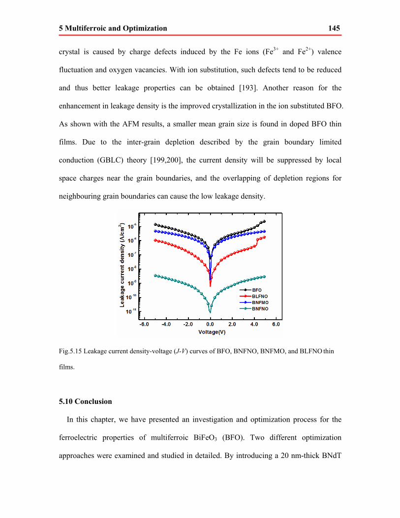
5 Multiferroic and Optimization 145
crystal is caused by charge defects induced by the Fe ions (Fe3+ and Fe2+) valence
fluctuation and oxygen vacancies. With ion substitution, such defects tend to be reduced
and thus better leakage properties can be obtained [193]. Another reason for the
enhancement in leakage density is the improved crystallization in the ion substituted BFO.
As shown with the AFM results, a smaller mean grain size is found in doped BFO thin
films. Due to the inter-grain depletion described by the grain boundary limited
conduction (GBLC) theory [199,200], the current density will be suppressed by local
space charges near the grain boundaries, and the overlapping of depletion regions for
neighbouring grain boundaries can cause the low leakage density.
Fig.5.15 Leakage current density-voltage (J-V) curves of BFO, BNFNO, BNFMO, and BLFNO thin
films.
5.10 Conclusion
In this chapter, we have presented an investigation and optimization process for the
ferroelectric properties of multiferroic BiFeO3 (BFO). Two different optimization
approaches were examined and studied in detailed. By introducing a 20 nm-thick BNdT
5 Multiferroic and Optimization 146
ferroelectric seeding layer, the structural and ferroelectric properties of BFO were
significantly improved, and room temperature ferroelectric hysteresis loops with
reasonable ferroelectric saturation were observed for the first time. This achievement can
be attributed to the inducing effect introduced by using the BNdT seeding layer to the
BFO upper layer. Many of the ferroelectric related properties, such as remanent
polarization, fatigue endurance, CV/IV, dielectric properties, and magnetic properties
were carefully studied and analyzed. Furthermore, we reported for the first time a dual-
site substitution technology for the BFO material. By adding La, Nd, Nb, and Mn
elements as the Fe-site and Bi-site substitutions, the volatile nature of the Bi and oxygen
vacancies was reconciled, and the leakage properties and therefore the ferroelectric
properties of BFO were optimized accordingly. Our work indicates that multilayer
technology and dual-site substitution are two effective approaches for improving the
room temperature performance of multiferroic BFO. With such technologies, BFO can be
optimized to exhibit a low leakage current density and good ferroelectric properties; thus
it may be a promising candidate in ferroelectrics-based applications.
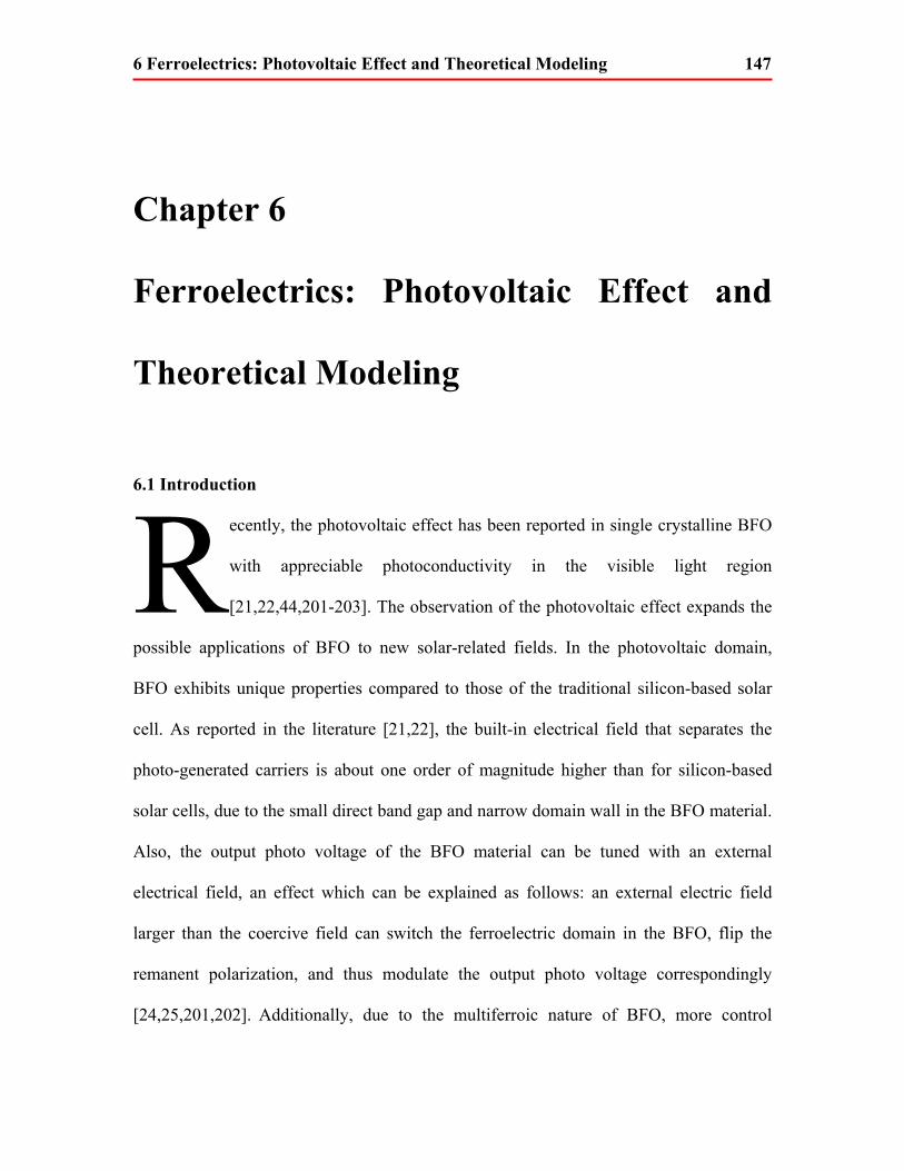
6 Ferroelectrics: Photovoltaic Effect and Theoretical Modeling 147
Chapter 6
Ferroelectrics: Photovoltaic Effect and
Theoretical Modeling
R6.1 Introduction
ecently, the photovoltaic effect has been reported in single crystalline BFO
with appreciable photoconductivity in the visible light region
[21,22,44,201-203]. The observation of the photovoltaic effect expands the
possible applications of BFO to new solar-related fields. In the photovoltaic domain,
BFO exhibits unique properties compared to those of the traditional silicon-based solar
cell. As reported in the literature [21,22], the built-in electrical field that separates the
photo-generated carriers is about one order of magnitude higher than for silicon-based
solar cells, due to the small direct band gap and narrow domain wall in the BFO material.
Also, the output photo voltage of the BFO material can be tuned with an external
electrical field, an effect which can be explained as follows: an external electric field
larger than the coercive field can switch the ferroelectric domain in the BFO, flip the
remanent polarization, and thus modulate the output photo voltage correspondingly
[24,25,201,202]. Additionally, due to the multiferroic nature of BFO, more control
6 Ferroelectrics: Photovoltaic Effect and Theoretical Modeling 148
mechanics including electricity, magnetism, heat, and stress can be employed to
manipulate the photovoltaic performance of the BFO material and therefore can be used
to provide solar cells with novel functionalities. However, most of the present studies are
focused on experimental work and little attention has been paid thus far to proposing any
theoretical or electrical models for describing the carrier mobility during the photovoltaic
process. Furthermore, all of the past studies have been conducted using Indium tin oxide
(ITO) and metals (Au and Pt) as top electrodes [45,46], without effort being spent in
finding replacements for the traditional ITO material.
In this chapter, we introduce the graphene sheet as a replacement for ITO material, and
we build a graphene/BFO/Pt photovoltaic heterostructure for the first time. An equivalent
electrical and thermal model is first proposed to aid in the understanding of the
transportation behaviour of the carriers. All important photovoltaic parameters are
investigated both experimentally and theoretically. More specifically, Section 6.2
introduces the five-step fabrication process for the graphene/BFO/Pt heterojunction.
Section 6.3 shows some basic performance characterizations of the BFO material and
graphene top electrode. In Section 6.4, we start by constructing the band diagram, and
then we establish an equivalent electrical model and calculate the theoretical photocurrent
J-V curves. In Section 6.5, we provide a detailed photovoltaic characterization of the
graphene/BFO/Pt heterojunction and using the theoretical model we investigate all
photovoltaic parameters experimentally and theoretically. Finally, this chapter is
summarized and concluded in Section 6.6.

6 Ferroelectrics: Photovoltaic Effect and Theoretical Modeling 149
6.2 Ferroelectric photovoltaic heterojunction fabrication
The fabrication process for the graphene/BFO/Pt photovoltaic heterojunction involves
five basic steps, as illustrated schematically in Fig.6.1 (a) to (e). To begin with, a BFO
precursor is prepared as discussed in the previous chapter. In the second step, a
polycrystalline BFO thin film of 300 nm is deposited onto a Pt(180 nm)/Ti(20
nm)/SiO2(300 nm)/Si(100) substrate using a sol-gel/spin coating process. Detailed
fabrication processes can be found in the previous chapter. At the next step, a single layer
polymethyl methacrylate (PMMA) thin film (~200 nm) with a circular window 3.5 mm in
diameter is coated on top of the BFO thin film as an isolation layer. In the fourth step, a
multilayer graphene sheet derived using an improved chemical vapor deposition (CVD)
method and transferred by PMMA is employed as the transparent electrodes. Finally,
silver paint is applied to the graphene film to make the contact for the electrical
measurement. Our as-prepared unit is also integrated into a package with an optical
window; a photograph of the as-packaged graphene/BFO/Pt photovoltaic heterojunction
is presented in Fig.5.1 (f) [204].
6 Ferroelectrics: Photovoltaic Effect and Theoretical Modeling 150
Fig.6.1 Schematic illustration of the fabrication process. (a) Synthesis of the BFO precursor. (b)
Deposition of the BFO crystal onto the Pt/Ti/SiO2/Si substrate. (c) Transfer of the PMMA isolation
film onto the as-prepared BFO crystal. (d) Transfer of the multilayer graphene sheet onto the PMMA
isolation window. (e) Deposition of the electrode contact. (f) Photograph of the packaged
graphene/BFO/Pt photovoltaic heterojunction.
6.3 Basic characterization
6.3.1 Graphene transparent electrode
Graphene is considered a promising candidate in the development of next generation
photovoltaic devices due to its attractive optical and electrical properties [205-209]. With
properties including a 2-dimensional (2D) atomic sheet structure, ballistic electronic
transport, ultra-high carrier mobility, high conductivity and transparency, good
mechanical strength, and flexibility, graphene has been the focus of a considerable

6 Ferroelectrics: Photovoltaic Effect and Theoretical Modeling 151
number of research studies [210-214]. Further, in the absence of the contact resistance in
CNT films caused by interconnected nanotube bundles, a continuous graphene sheet can
exhibit high conductivity at ultra-low thicknesses (~atomic range) [213-215]. Several
solar applications that use graphene as transparent/conductive electrodes have been
investigated in depth, and exhibit interesting prospects for future application development
[209,216-219]. Inspired by the unique optical properties of grapheme and its superiority
in stability, transparency, and conductivity compared with ITO, we chose a graphene
sheet as the transparent electrode in this BFO photovoltaic device.
A scanning electron microscope (SEM) image, shown in Fig.6.2, depicts the surface
topography of the as-grown graphene sheet. A smooth and dense surface can be identified
over a wide lateral scale. The Raman scattering spectrum, shown in Fig.6.2, reveals the
multilayer nature of the as-prepared graphene sheet. The expected G and 2D bands with
full width at half maximums (FWHM) of 16 and 34 cm-1 can be indexed at the positions
1589 and 2685 cm-1, respectively. Both peaks can be fitted using a single Lorentzian
function that exhibits a symmetric and sharp shape. The distribution of the peak intensity
ratio between the 2D and G bands, as shown with 2D micro-Raman mapping (Fig.2 (c)),
further confirms the multilayer pattern, as well as the uniformity and consistency of the
graphene film achieved. Furthermore, the negligible D band implies that the grapheme
sheet obtained from this experiment is of high quality and is defect-free. As reported by S.
Bae et al. [220], the transparency and the sheet resistance both decrease as the graphene
sheet thickness increases, indicating a trade-off between transparency and resistance. In
our experiment, a multilayer graphene sheet with much lower sheet resistance and
slightly inferior transparency compared with those of a monolayer graphene film is

6 Ferroelectrics: Photovoltaic Effect and Theoretical Modeling 152
introduced as the transparent electrode, and this sheet exhibits optimized photovoltaic
performance.
Fig.6.2 SEM top view morphology of the as-deposited graphene film.

6 Ferroelectrics: Photovoltaic Effect and Theoretical Modeling 153
Fig.6.3 (a) Raman spectrum of as-deposited graphene showing G and 2D peaks. 2D micro-Raman
intensity mapping of (b) G band (1589 cm-1) and (c) 2D band (2685 cm-1). (d) 2D micro-Raman
intensity ratio (I2D/IG) mapping from the same regions as (b) and (c).
A high optical transparency (~90%) of the as-prepared graphene sheet is seen from the
UV-vis transmission spectrum shown in Fig.6.4. An optical quartz substrate is used to
minimize the optical absorption in the UV range. Since the optical transmission of the
monolayer graphene film is reported to be ~97% and it is usually degraded by ~2.2-2.3%
for each additional graphene layer [221], our transmission result further confirms the
multilayer nature of the graphene film obtained in this experiment.
Fig.6.4 UV-vis transmission spectrum of the as-prepared graphene sheet.
6.3.2 BFO characterization
In order to verify the ferroelectric performance of BFO in the graphene/BFO/Pt
heterojunction structure, some basic structural characterizations are performed for the
BFO thin film. Fig.6.5 (a) provides the X-ray diffraction (XRD) pattern of the as-
prepared BFO thin films, indicating polycrystalline behaviour without any preferred
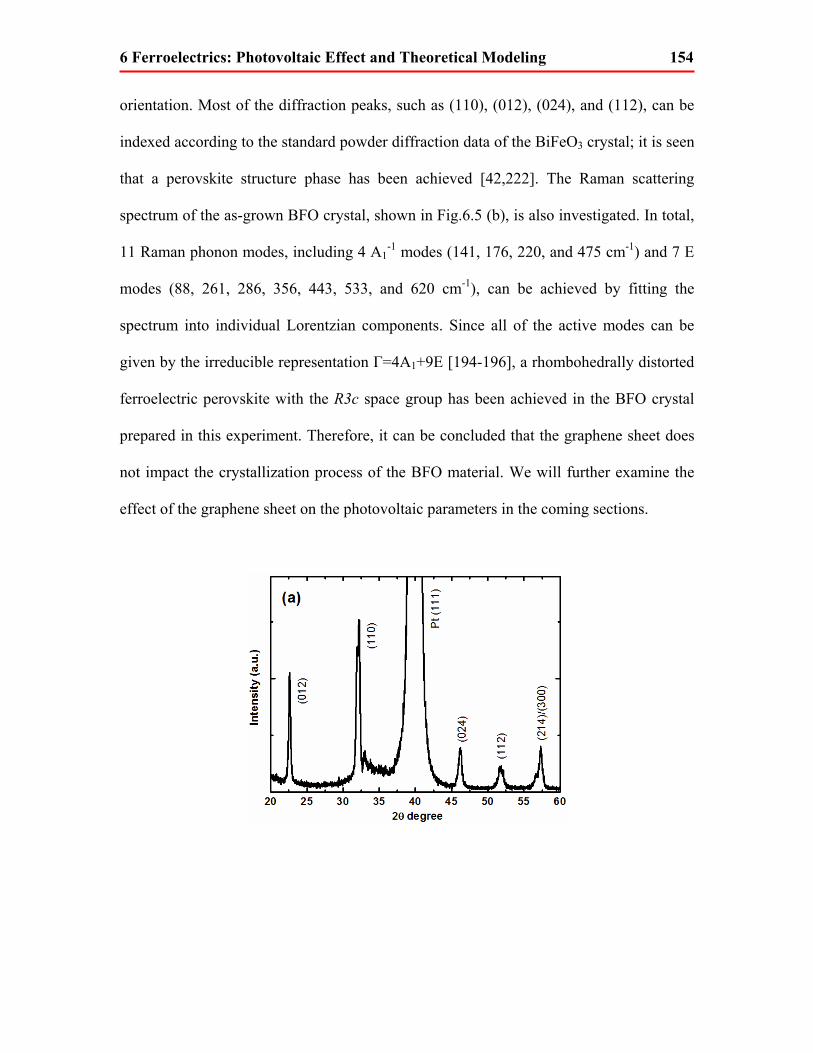
6 Ferroelectrics: Photovoltaic Effect and Theoretical Modeling 154
orientation. Most of the diffraction peaks, such as (110), (012), (024), and (112), can be
indexed according to the standard powder diffraction data of the BiFeO3 crystal; it is seen
that a perovskite structure phase has been achieved [42,222]. The Raman scattering
spectrum of the as-grown BFO crystal, shown in Fig.6.5 (b), is also investigated. In total,
11 Raman phonon modes, including 4 A1-1 modes (141, 176, 220, and 475 cm-1) and 7 E
modes (88, 261, 286, 356, 443, 533, and 620 cm-1), can be achieved by fitting the
spectrum into individual Lorentzian components. Since all of the active modes can be
given by the irreducible representation Г=4A1+9E [194-196], a rhombohedrally distorted
ferroelectric perovskite with the R3c space group has been achieved in the BFO crystal
prepared in this experiment. Therefore, it can be concluded that the graphene sheet does
not impact the crystallization process of the BFO material. We will further examine the
effect of the graphene sheet on the photovoltaic parameters in the coming sections.
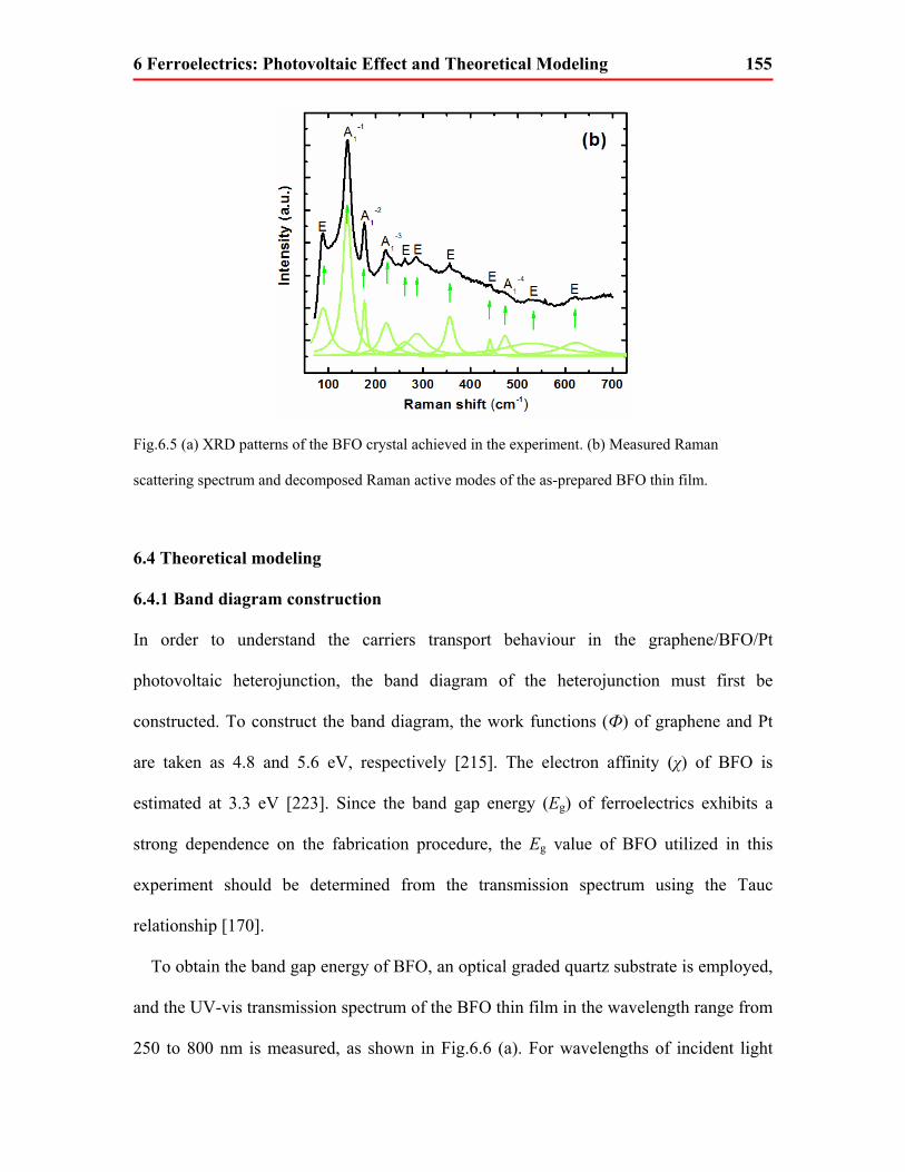
6 Ferroelectrics: Photovoltaic Effect and Theoretical Modeling 155
Fig.6.5 (a) XRD patterns of the BFO crystal achieved in the experiment. (b) Measured Raman
scattering spectrum and decomposed Raman active modes of the as-prepared BFO thin film.
6.4 Theoretical modeling
6.4.1 Band diagram construction
In order to understand the carriers transport behaviour in the graphene/BFO/Pt
photovoltaic heterojunction, the band diagram of the heterojunction must first be
constructed. To construct the band diagram, the work functions (Ф) of graphene and Pt
are taken as 4.8 and 5.6 eV, respectively [215]. The electron affinity (χ) of BFO is
estimated at 3.3 eV [223]. Since the band gap energy (Eg) of ferroelectrics exhibits a
strong dependence on the fabrication procedure, the Eg value of BFO utilized in this
experiment should be determined from the transmission spectrum using the Tauc
relationship [170].
To obtain the band gap energy of BFO, an optical graded quartz substrate is employed,
and the UV-vis transmission spectrum of the BFO thin film in the wavelength range from
250 to 800 nm is measured, as shown in Fig.6.6 (a). For wavelengths of incident light
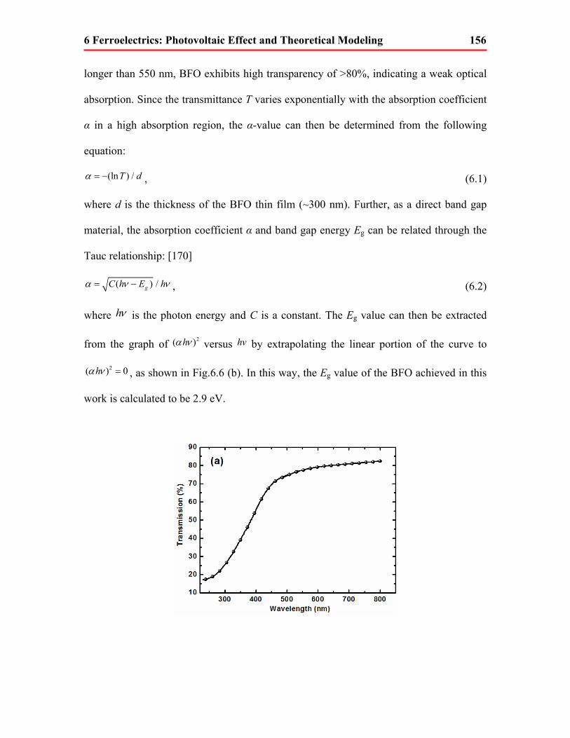
6 Ferroelectrics: Photovoltaic Effect and Theoretical Modeling 156
longer than 550 nm, BFO exhibits high transparency of >80%, indicating a weak optical
absorption. Since the transmittance T varies exponentially with the absorption coefficient
α in a high absorption region, the α-value can then be determined from the following
equation:
(ln ) /T dα = − , (6.1)
where d is the thickness of the BFO thin film (~300 nm). Further, as a direct band gap
material, the absorption coefficient α and band gap energy Eg can be related through the
Tauc relationship: [170]
( ) /gC h E hα ν ν= − , (6.2)
where hν is the photon energy and C is a constant. The Eg value can then be extracted
from the graph of 2( )hα ν versus hv by extrapolating the linear portion of the curve to
2( )hα ν = 0 , as shown in Fig.6.6 (b). In this way, the Eg value of the BFO achieved in this
work is calculated to be 2.9 eV.

6 Ferroelectrics: Photovoltaic Effect and Theoretical Modeling 157
Fig.6.6 (a) Optical transmittance of the as-grown BFO crystal. (b) Photon energy dependence of the
optical absorption coefficient in the as-prepared BFO thin film.
Given the values listed above, we can construct the band diagram. When BFO and
graphene or Pt are joined together, two Schottky barriers will be formed and the barriers
at both interfaces will inhibit the Schottky emission, forming two built-in electrical fields
in opposite directions. This band diagram, which is simulated in the next section, is
referred to as the “virgin state”, where two Schottky junctions serve as back-to-back
diodes and no current can be measured regardless of the polarity of the applied electrical
field. However, as reported by C. Wang and C. Ge, et al. [224,225], the ferroelectric
remanent polarization Pr caused by an external electrical field will charge the neutral
oxygen vacancy. The released electrons, along with the depolarization field and interface
states, will form a narrow positive/negative charged region near the interface, resulting in
an “upward/downward band bending” at the graphene/BFO and BFO/Pt interfaces.
More specifically, when BFO and graphene or Pt are joined, two Schottky barriers
will be formed with two built-in fields in opposite directions [204]. The two interface

6 Ferroelectrics: Photovoltaic Effect and Theoretical Modeling 158
junctions are both depleted. The width of the depletion region (xdc) can be given as
follows:
02 s sdc
D
VxqNε ε
= , (6.3)
where, 0ε is the vacuum permittivity, sε is the relative dielectric constant of the BFO
material, DN is the carrier density, and SV is the surface potential defined as:
dcS x surface x xV V V== − = , (6.4)
which can be used to describe the potential barrier difference between the surface and
body, and represents the band bending.
By calculating the widths of the depletion regions at both the graphene/BFO and
BFO/Pt sides, it can be found that the entire width of the two depletion regions (~ 500 nm)
is larger than the BFO thickness (~300 nm) in this experiment. Therefore, the entire BFO
thin film is depleted across the top and bottom electrodes without any neutral region.
Thus, the modified Poisson Equation can be applied at both interfaces of
graphene/BFO and BFO/Pt [204]:
2
0
1( , , ) ( ( , , ) ( , , ))rs
V x y z x y z P x y zρε ε
∇ = − −∇⋅, (6.5)
where ( , , )V x y z is the voltage potential, ( , , )x y zρ is the charge density, ( , , )rP x y z is the
ferroelectric remnant polarization, 0ε is the vacuum permittivity, and sε is the relative
dielectric constant of BFO.
To simplify the calculation we examine the one-dimensional case, for which Eq. (6.5)
is written as follows:
6 Ferroelectrics: Photovoltaic Effect and Theoretical Modeling 159
2
20
( )( ) 1 ( ( ) )r
s
dP xd V x xdx dx
ρε ε
= − − . (6.6)
Further, ( )xρ can be determined from:
( ) [ ( ) ( ) ( ) ( )]D Ax q p x p x n x n xρ = + − − , (6.7)
where ( )n x and ( )p x are the electron and hole density, respectively; and ( )An x and
( )Dp x are the ionized donor and acceptor density, respectively. Here, we can assume that
electrons and holes can be described by the Fermi Distribution:
( )/0
( )/0
( )( )
B
B
qV x K T
qV x K T
n x n ep x p e−
⎫=⎬
= ⎭, (6.8)
where 0n and 0p are the electron and hole density, respectively, at thermal equilibrium.
Also, 0 Dn N≈ , and BK is the Boltzmann constant.
When the electro neutrality condition 0 0[ D Aq p p n n ] 0+ − − = is met, then
0D A 0p n n p− = − . (6.9)
For completeness, it is noted that:
( ) ( )B
qV x u xK T
= . (6.10)
Therefore, Eq. (6.7) can be rewritten as follows:
0 0( ) [ ( 1) ( 1)]u ux q p e n eρ −= − − − . (6.11)
For BFO, ,therefore Eq. (6.9) can be simplified as 0n >> 0p
0( ) ( 1)ux qn eρ = − − . (6.12)
Pr(x) can be calculated by
6 Ferroelectrics: Photovoltaic Effect and Theoretical Modeling 160
max
max
( ) ( )rr
c
PP x E xE
= c , (6.13)
where maxrP and maxcE represent the remnant polarization and the coercive field in the
saturated polarization-electric field (P-E) hysteresis loop, respectively, and EC is the
electric field.
Therefore, Eq. (6.6) can be given as,
2
020
( )( ) 1 [ ( 1)u r
s
dP xd V x qn edx dxε ε
= − + ] , (6.12)
Then using Taylor expansion,
2
1 ... ...2 !
nu u ue u
n− = + + + + ,
we can subsequently solve Eq.(6.11).
In a one-dimensional scenario, by taking the interface state into account, the boundary
conditions during the derivation process can be expressed as:
(0) sGS BFO GS BFOV V −= = Φ −Φ (6.13)
( ) sBFO Pt BFO PtV L V −= = Φ −Φ , (6.14)
where L is the thickness of the BFO thin film, and sGS BFOV − and sBFO PtV − are the surface
potentials at graphene/BFO and BFO/Pt, respectively.
By applying these boundary conditions, three possible energy band diagrams of the
graphene/BFO/Pt heterojunction can be simulated using MATLAB®; these are given in
Fig.6.7 (a)-(c), where a switchable diode in series with a variable resistance is used in the
theoretical model of the graphene/BFO/Pt heterojunction.

6 Ferroelectrics: Photovoltaic Effect and Theoretical Modeling 161
Virgin states
Fig.6.7 (a) Depletion regions are formed on both sides. Such a band diagram is equivalent to two
back-to-back diodes, and no current will be observed regardless of whether the applied voltage is
positive or negative.
Upward bending
Fig.6.7 (b) Electrons are accumulated at the graphene/BFO side and can be regarded as a variable
resistance. The BFO/Pt side is depleted and can be treated as a Schottky diode.

6 Ferroelectrics: Photovoltaic Effect and Theoretical Modeling 162
Downward bending
Fig.6.7 (c) Electrons are accumulated at the BFO/Pt side and can be regarded as a variable resistance.
The graphene/BFO side is depleted and can be treated as a Schottky diode.
6.4.2 Theoretical J-V model
As explained above, interface trapped charges and a high enough electric field will switch
the ferroelectric polarization in the BFO thin film and stimulate neutral oxygen vacancies
to release electrons, forming a narrow electron region near the interface and resulting in
energy band bending.
When a positive electrode is connected to the Pt electrode, a depletion region will be
formed at the BFO/Pt side, as shown in Fig.6.7 (b).
When the diffusion model dominates, the current density can be written as:
(B F
B B
q qVK T K T
n Cj q EN e eΦ
μ−
= 1)− , (6.15)
where nμ is the electron mobility, 3/2
22( )2dn B
Cm K TNπ
= is equivalent density of states at
the bottom of conduction band, dnm is the effective mass of an electron, BΦ is the built-in
6 Ferroelectrics: Photovoltaic Effect and Theoretical Modeling 163
potential, and FV is the junction bias. Also, E is the electrical field of the space charge
region, and can be defined as:
( )0
2 D i F
s
qN VE
φε ε
−= , (6.16)
where (dci C x surf C x x ) /E E qφ = == − represents the band bending.
When the thermal emission model dominates, the current density can be written as:
* 2 (B F
B B
q qVK T K Tj A T e eΦ
−
= 1)− , (6.17)
where* 4 dn BA qm Kπ= 2 3/ h is the Richardson constant.
In our experiment, the BFO thin film is prepared using the sol-gel process, and thus the
two models described above should both be taken into account. The optimized current
density can be described as:
( 14
B F
B B
q qVK T K TV
D
qvNj e evv
Φ−
= −+
), (6.18)
where VF is the junction bias, ( )128 /B pv K T mπ= is the average thermal velocity, NC is the
equivalent density of states, BΦ is the built-in potential,
( )( )12
02 /D D i Fv nE n qN V sμ μ φ ε= = − ε is the carrier drift velocity, and
(dci C x surf C x xE Eφ = == − ) / q represents the band bending with xdc as the junction width.
6.4.3 Equivalent electrical model construction
Electrons are accumulated at the graphene/BFO side and can be modeled as a variable
resistance,

6 Ferroelectrics: Photovoltaic Effect and Theoretical Modeling 164
p nqp qn qn nσ μ μ= + ≈ μ , (6.19)
which can be regarded as constant. In fact, the width of the depletion region will change
with different external applied voltages, and the resistance will vary as follows:
1 ( dc )R L xσ
= − . (6.20)
Vice versa, when the positive electrode is connected to the graphene electrode, a
depletion region will be formed at the graphene/BFO side, as shown in Fig.6.7 (c), and a
similar analysis to above can be applied.
The equivalent electrical model is obtained based on this analysis. The corresponding
circuit diagram is shown in Fig.6.8.
Fig.6.8 Equivalent electrical model of the graphene/BFO/Pt heterojunction.
In Fig.6.8, S1 and S2 are the Schottky barrier diodes, Rs1 and Rs2 are the variable
resistances, Rc1 and Rc2 are the contact resistances of BFO with the graphene and Pt
electrodes, R is the edge resistance caused by imperfect factors, and C1 to C4 are the
junction capacitances. Jp1 and Jp2 are introduced to characterize the photocurrent term
upon illumination.

6 Ferroelectrics: Photovoltaic Effect and Theoretical Modeling 165
According to this electrical model, the short circuit current should be zero without
illumination. However, interface trapped charges offer a weak ferroelectric polarization δ
at the interface, leading to a weak band bending and a sub on-state of the diode even at
zero bias, resulting in a non-zero dark current. Therefore, a voltage source Vsub is added
to characterize the I-V curve offset at zero bias.
Moreover, the electrical model should be dynamic and flexible for use in a practical
application. The parameters of diodes S1 and S2, such as the width of depletion region,
potential barrier height, and so forth, will vary with different applied voltages. In order to
simplify our model, the parameters of S1 and S2 are set using an approximation, and a
current supply JR is introduced to describe such circuit parameter induced current
variation and leakage terms in the heterojunction.
The modified equivalent electrical model is given in Fig.6.9. This equivalent electrical
model, along with the band diagram model, will be applied to characterize the electrical
and optical properties of the graphene/BFO/Pt photovoltaic heterojunction in the coming
sections.
Fig.6.9. Modified equivalent electrical model of the graphene/BFO/Pt heterojunction.
6 Ferroelectrics: Photovoltaic Effect and Theoretical Modeling 166
6.5 Photovoltaic characterization
6.5.1 Dark current properties
The dark current density of the graphene/BFO/Pt heterojunction is measured and plotted
in Fig.6.10. A simulated dark current density derived from the equivalent electrical model
and from Eq.(6.18) is also presented, and is in good agreement with the experimental
result. As shown in Fig.6.10, the dark current exhibits a substantial current density of 2.3
μA/cm2 at zero bias; this current density can be characterized by the voltage source Vsub
in the electrical model. The non-zero short circuit dark current can be attributed to the
remanent ferroelectric polarization δ at the interface. As explained above, an external
electrical field will polarize the ferroelectric material BFO, trapping some charge at the
interface, leading to a “bending” of the heterojunction band diagram and a sub on-state of
the diodes (S1 and S2) shown in the electrical model, resulting in the non-zero dark
current [204].
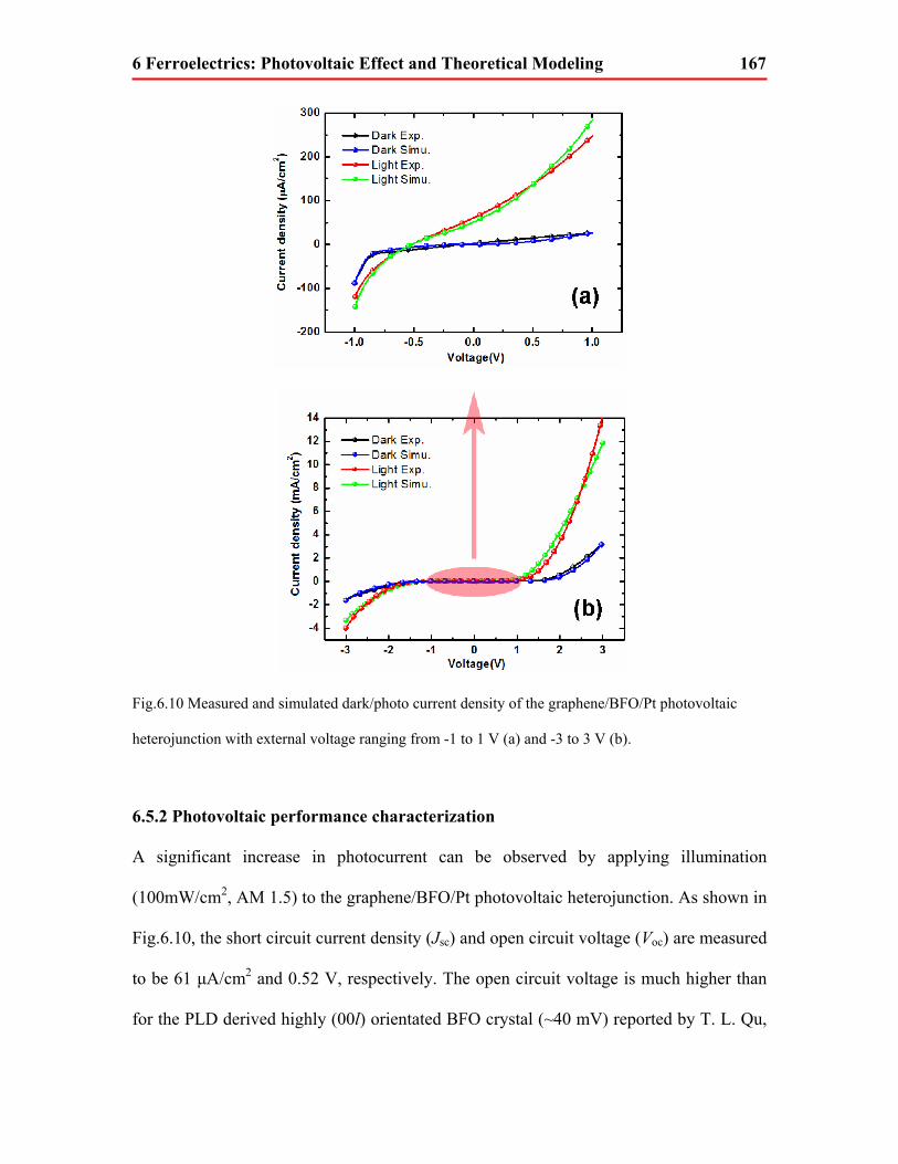
6 Ferroelectrics: Photovoltaic Effect and Theoretical Modeling 167
Fig.6.10 Measured and simulated dark/photo current density of the graphene/BFO/Pt photovoltaic
heterojunction with external voltage ranging from -1 to 1 V (a) and -3 to 3 V (b).
6.5.2 Photovoltaic performance characterization
A significant increase in photocurrent can be observed by applying illumination
(100mW/cm2, AM 1.5) to the graphene/BFO/Pt photovoltaic heterojunction. As shown in
Fig.6.10, the short circuit current density (Jsc) and open circuit voltage (Voc) are measured
to be 61 μA/cm2 and 0.52 V, respectively. The open circuit voltage is much higher than
for the PLD derived highly (00l) orientated BFO crystal (~40 mV) reported by T. L. Qu,

6 Ferroelectrics: Photovoltaic Effect and Theoretical Modeling 168
et al. [46], and the sol-gel fabricated polycrystalline BFO (~0.08 V) with an ITO
electrode [45]. This obvious improvement in photovoltaic performance can be attributed
to the superior properties of graphene compared to the traditional ITO electrode. First, the
optical transparency of the graphene sheet is higher than for ITO [220], allowing more
light to pass through the transparent electrode. Second, the flexible nature of the graphene
sheet provides a better electrical contact with the BFO crystal, reducing the contact
resistance and resulting in better photovoltaic performance. Third, the theoretical carrier
mobility of graphene is much higher than for the ITO material, and an experimental result
of ~7×104 cm2/V·s was recently reported using single crystal PZT as the substrate [226].
The weak power conversion efficiency, which can be attributed to the relatively large
band gap of the BFO material, is found to be ~8.0×10⁻³ %. This result is comparable with
the value (~3×10⁻³ %) reported by T. Choi et al. [21], and is larger than that of ~7×10⁻⁴ %
reported by W. Ji et al. [44].
To obtain the theoretical photocurrent density upon illumination, Eq. (6.18) is rewritten
as follows:
( )L F E L T dkI I I A j A j V= − = − , (6.21)
where 0 0( )[1 ( )]dcx x
L 0j q e α dxdβΦ λ ρ λ α λ∞ −= −∫ ∫ , (6.22)
EA is the illumination area, TA is the cell area, Lj is the photocurrent density, dkj is the
dark current density, β is the generation coefficient, Φ0 is the intensity of photons at
wavelength λ , ρ is the reflectance, and α is the absorption coefficient. Using Eq.
(6.21)-(6.22), the simulated light photocurrent density is plotted and compared with the
experimental result, as shown in Fig.6.10. This comparison indicates a good consistency
in results. It is concluded from both simulated and experimental curves that the
6 Ferroelectrics: Photovoltaic Effect and Theoretical Modeling 169
photocurrent density is not symmetric with applied voltage, that is, the forward portion
exhibits faster growth rate under an applied voltage than does the reversed segment. This
discrepancy is explained by the difference in potential barrier heights at the two
interfaces. Since the photo generated carriers are separated by the built-in electrical field
at the interface, the height of the Schottky barrier plays a critical role in determining the
photocurrent density. Upon forward bias, when a positive voltage is applied to the Pt
substrate, the Schottky junction on the BFO/Pt side is equivalent to a Schottky diode
which promotes the photocurrent; the Schottky junction on the graphene/BFO side can be
regarded as a resistance. The functionality of these two Schottky junctions will be
switched upon reverse bias. Since the potential barrier is much higher on the BFO/Pt side
(2.7 eV) compared to the graphene/BFO interface (1.9 eV), a stronger built-in electrical
field and thus faster growth rate can be observed upon forward bias compared with the
reversed bias [104].
6.5.3 Illumination intensity dependence
The short circuit photocurrent of the graphene/BFO/Pt heterojunction for incident light
intensities from 0.8 AM to 1.4 AM is also measured and presented in Fig.6.11 (a). It can
be seen that Jsc varies proportionally with incident light intensity, which is consistent
with the increase in light-induced photo carriers upon an increase in light intensity.
To further confirm the photoconductivity variation under different illumination
intensities, conductive AFM (CAFM) is used to examine the local current behaviour and
leakage path distribution on a microscopic level. Equipped with a conductive tip, CAFM
is considered an effective method for investigating the local conductivity of dielectric
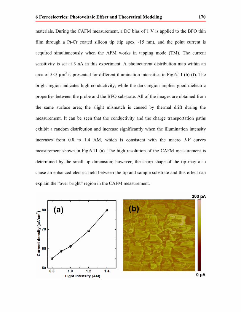
6 Ferroelectrics: Photovoltaic Effect and Theoretical Modeling 170
materials. During the CAFM measurement, a DC bias of 1 V is applied to the BFO thin
film through a Pt-Cr coated silicon tip (tip apex ~15 nm), and the point current is
acquired simultaneously when the AFM works in tapping mode (TM). The current
sensitivity is set at 3 nA in this experiment. A photocurrent distribution map within an
area of 5×5 µm2 is presented for different illumination intensities in Fig.6.11 (b)-(f). The
bright region indicates high conductivity, while the dark region implies good dielectric
properties between the probe and the BFO substrate. All of the images are obtained from
the same surface area; the slight mismatch is caused by thermal drift during the
measurement. It can be seen that the conductivity and the charge transportation paths
exhibit a random distribution and increase significantly when the illumination intensity
increases from 0.8 to 1.4 AM, which is consistent with the macro J-V curves
measurement shown in Fig.6.11 (a). The high resolution of the CAFM measurement is
determined by the small tip dimension; however, the sharp shape of the tip may also
cause an enhanced electric field between the tip and sample substrate and this effect can
explain the “over bright” region in the CAFM measurement.
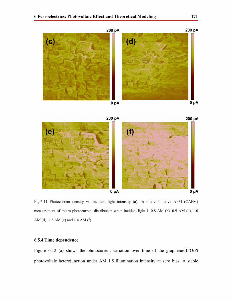
6 Ferroelectrics: Photovoltaic Effect and Theoretical Modeling 171
Fig.6.11 Photocurrent density vs. incident light intensity (a). In situ conductive AFM (CAFM)
measurement of micro photocurrent distribution when incident light is 0.8 AM (b), 0.9 AM (c), 1.0
AM (d), 1.2 AM (e) and 1.4 AM (f).
6.5.4 Time dependence
Figure 6.12 (a) shows the photocurrent variation over time of the graphene/BFO/Pt
photovoltaic heterojunction under AM 1.5 illumination intensity at zero bias. A stable
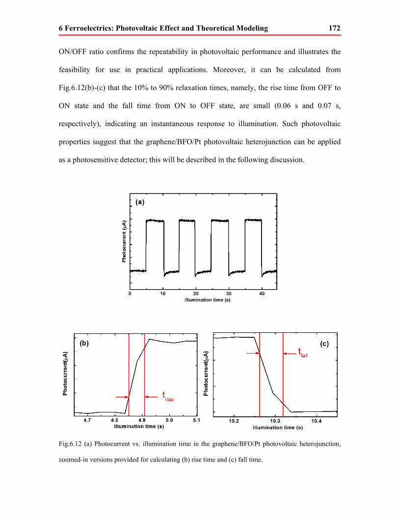
6 Ferroelectrics: Photovoltaic Effect and Theoretical Modeling 172
ON/OFF ratio confirms the repeatability in photovoltaic performance and illustrates the
feasibility for use in practical applications. Moreover, it can be calculated from
Fig.6.12(b)-(c) that the 10% to 90% relaxation times, namely, the rise time from OFF to
ON state and the fall time from ON to OFF state, are small (0.06 s and 0.07 s,
respectively), indicating an instantaneous response to illumination. Such photovoltaic
properties suggest that the graphene/BFO/Pt photovoltaic heterojunction can be applied
as a photosensitive detector; this will be described in the following discussion.
Fig.6.12 (a) Photocurrent vs. illumination time in the graphene/BFO/Pt photovoltaic heterojunction,
zoomed-in versions provided for calculating (b) rise time and (c) fall time.
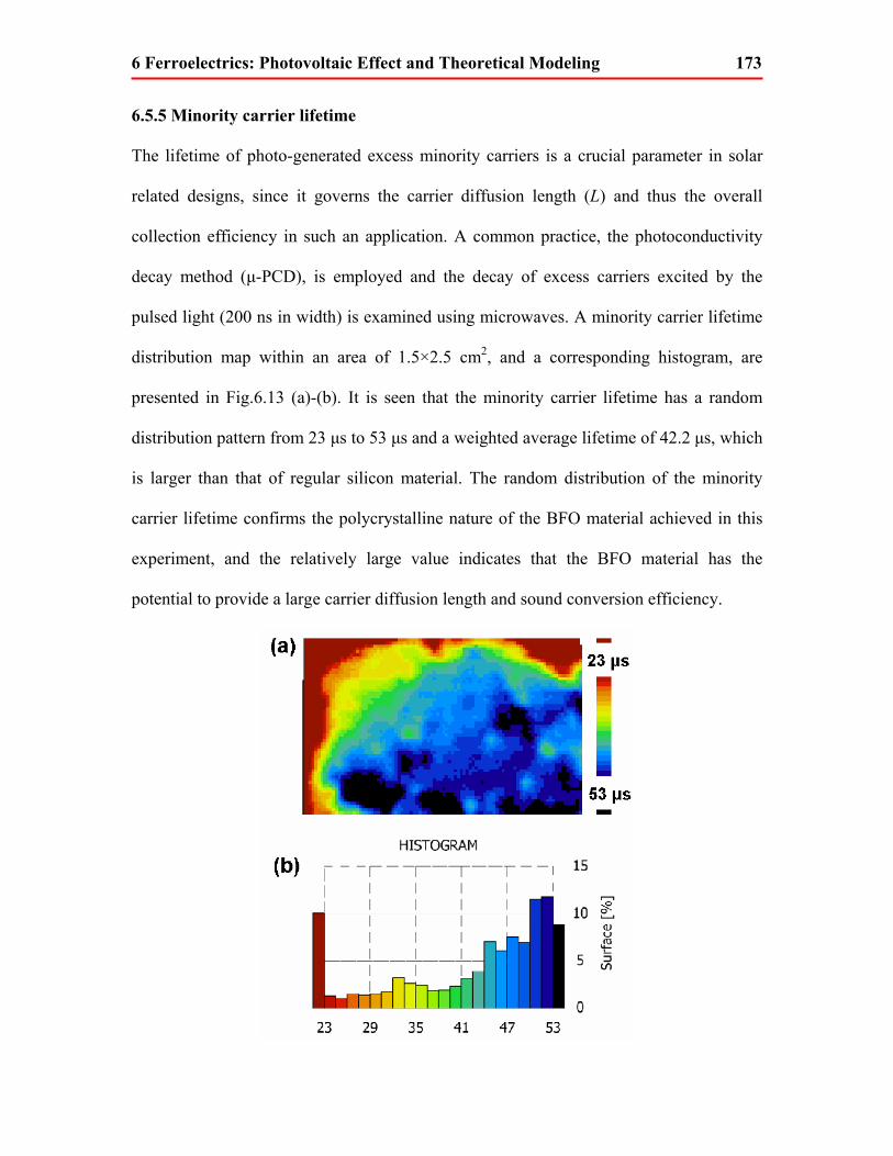
6 Ferroelectrics: Photovoltaic Effect and Theoretical Modeling 173
6.5.5 Minority carrier lifetime
The lifetime of photo-generated excess minority carriers is a crucial parameter in solar
related designs, since it governs the carrier diffusion length (L) and thus the overall
collection efficiency in such an application. A common practice, the photoconductivity
decay method (μ-PCD), is employed and the decay of excess carriers excited by the
pulsed light (200 ns in width) is examined using microwaves. A minority carrier lifetime
distribution map within an area of 1.5×2.5 cm2, and a corresponding histogram, are
presented in Fig.6.13 (a)-(b). It is seen that the minority carrier lifetime has a random
distribution pattern from 23 μs to 53 μs and a weighted average lifetime of 42.2 μs, which
is larger than that of regular silicon material. The random distribution of the minority
carrier lifetime confirms the polycrystalline nature of the BFO material achieved in this
experiment, and the relatively large value indicates that the BFO material has the
potential to provide a large carrier diffusion length and sound conversion efficiency.

6 Ferroelectrics: Photovoltaic Effect and Theoretical Modeling 174
Fig.6.13 Minority carrier lifetime mapping of the BFO crystal in a region of 1.5×2.5 cm2 (a) and the
corresponding distribution histogram (b).
6.5.6 External quantum efficiency
External quantum efficiency (EQE), an important parameter that quantitatively defines
the conversion percentage of an incident photon into an electron-hole pair, is also
investigated and plotted in Fig.6.14. The photo conversion efficiency of the
graphene/BFO/Pt photovoltaic heterojunction over a wavelength range from 250 to 900
nm is presented. It shows a maximum harvest efficiency of 1.42% around 417 nm,
corresponding to the band gap energy of the BFO material calculated above. The low
EQE in other wavelength regions can be attributed to the poor excitons
stimulation/dissociation and material absorption. As for most photographic films, the
BFO thin film has EQE values of much less than 10%, indicating weak conversion
efficiency.
Fig.6.14. External quantum efficiency (EQE) measurement of the graphene/BFO/Pt photovoltaic
heterojunction.
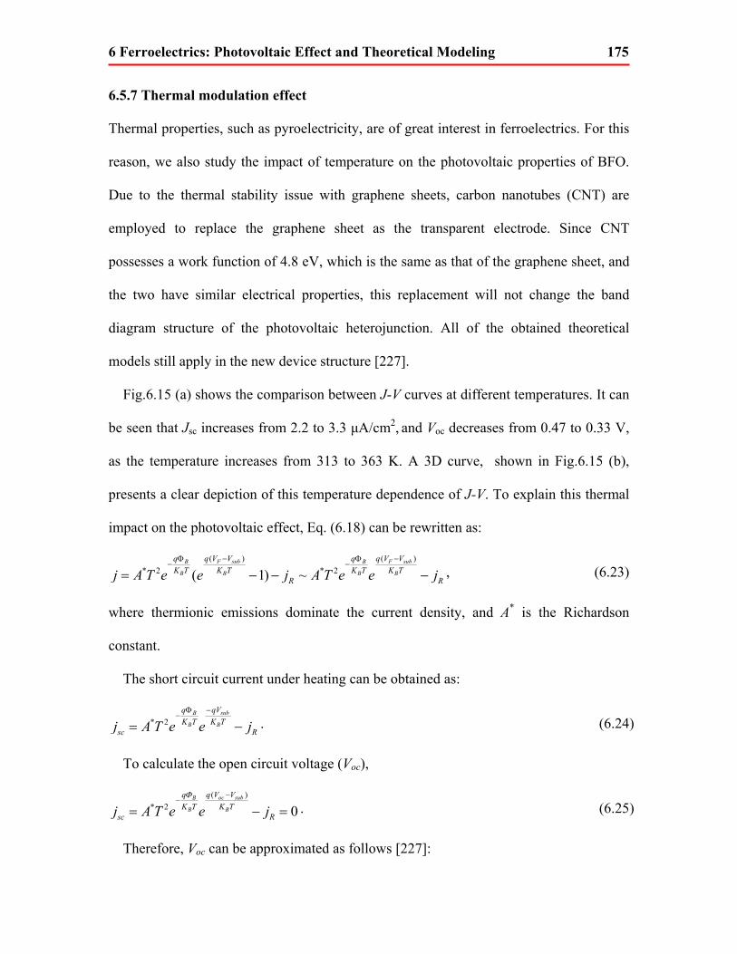
6 Ferroelectrics: Photovoltaic Effect and Theoretical Modeling 175
6.5.7 Thermal modulation effect
Thermal properties, such as pyroelectricity, are of great interest in ferroelectrics. For this
reason, we also study the impact of temperature on the photovoltaic properties of BFO.
Due to the thermal stability issue with graphene sheets, carbon nanotubes (CNT) are
employed to replace the graphene sheet as the transparent electrode. Since CNT
possesses a work function of 4.8 eV, which is the same as that of the graphene sheet, and
the two have similar electrical properties, this replacement will not change the band
diagram structure of the photovoltaic heterojunction. All of the obtained theoretical
models still apply in the new device structure [227].
Fig.6.15 (a) shows the comparison between J-V curves at different temperatures. It can
be seen that Jsc increases from 2.2 to 3.3 μA/cm2, and Voc decreases from 0.47 to 0.33 V,
as the temperature increases from 313 to 363 K. A 3D curve, shown in Fig.6.15 (b),
presents a clear depiction of this temperature dependence of J-V. To explain this thermal
impact on the photovoltaic effect, Eq. (6.18) can be rewritten as:
( ) ( )* 2 * 2( 1) ~
F sub F subB
B B B B
q V V q V Vq qK T K T K T K T
R
B
Rj A T e e j A T e e j− −Φ Φ
− −
= − − − , (6.23)
where thermionic emissions dominate the current density, and A* is the Richardson
constant.
The short circuit current under heating can be obtained as:
* 2subB
B B
qVqK T K T
sc Rj A T e e j−Φ
−
= − . (6.24)
To calculate the open circuit voltage (Voc),
( )* 2 0
oc subB
B B
q V VqK T K T
sc Rj A T e e jΦ −
−
= − = . (6.25)
Therefore, Voc can be approximated as follows [227]:
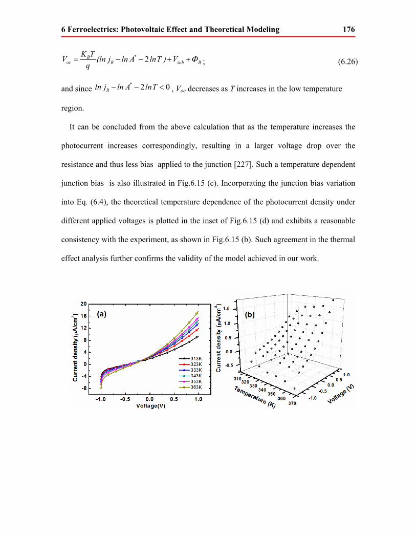
6 Ferroelectrics: Photovoltaic Effect and Theoretical Modeling 176
2*Boc R sub B
K TV (ln j ln A lnT ) Vq
Φ= − − + + ; (6.26)
and since 2*Rln j ln A lnT− − < 0 , Voc decreases as T increases in the low temperature
region.
It can be concluded from the above calculation that as the temperature increases the
photocurrent increases correspondingly, resulting in a larger voltage drop over the
resistance and thus less bias applied to the junction [227]. Such a temperature dependent
junction bias is also illustrated in Fig.6.15 (c). Incorporating the junction bias variation
into Eq. (6.4), the theoretical temperature dependence of the photocurrent density under
different applied voltages is plotted in the inset of Fig.6.15 (d) and exhibits a reasonable
consistency with the experiment, as shown in Fig.6.15 (b). Such agreement in the thermal
effect analysis further confirms the validity of the model achieved in our work.

6 Ferroelectrics: Photovoltaic Effect and Theoretical Modeling 177
Fig.6.15. (a) J-V curves for different temperatures (313 to 373 K). (b) A 3D view of the
temperature/voltage dependence of the photocurrent density. (c) Simulated temperature dependence of
the junction bias. (d) Temperature dependence of the photocurrent density under different applied
voltages (-1 to 1 V); in the bottom left inset is the simulated temperature dependence of J-V.
6.6 Conclusion
Research on the photovoltaic effect of multiferroic BFO is a new hot spot in the
ferroelectric field. In this chapter, we demonstrated an enhancement in the photovoltaic
performance of a polycrystalline BFO thin film with graphene as the top electrode. The
short circuit current density (Jsc) and open circuit voltage (Voc) of the heterojunction were
measured to be 61 μA/cm2 and 0.52 V, respectively, values which are much higher than
those reported for polycrystalline BFO with indium tin oxide (ITO) as the top electrode.
A theoretical band diagram model and an equivalent electrical model, considering the
ferroelectric polarization, interface states, and energy band bending effect, were
constructed to describe the carrier transportation behaviour. A detailed photovoltaic
characterization of the graphene/BFO/Pt heterojunction was performed. Different
photovoltaic parameters, including dark/light properties, illumination intensity
dependence, time dependence, minority carrier lifetime, external quantum efficiency, and

6 Ferroelectrics: Photovoltaic Effect and Theoretical Modeling 178
the thermal modulation effect, were investigated experimentally and theoretically. Our
work indicates that by introducing graphene as a replacement for the ITO material, the
photovoltaic performance of BFO has been improved significantly, making the
graphene/polycrystalline BFO/Pt heterojunction a promising candidate for next
generation photovoltaic-related applications.

7 Photovoltaic Performance Enhancement and Applications 179
Chapter 7
Photovoltaic Performance Enhancement
and Applications
7.1 Introdu
n the previous chapter, we examined photovoltaic-related parameters of the
graphene/BFO/Pt photovoltaic heterojunction, and demonstrated the promising
properties and performance of BFO. In this chapter, we will further our research
on enhancing the performance and photovoltaic applications. Although the
graphene/BFO/Pt photovoltaic heterojunction demonstrates superior properties compared
with such devices reported in the literature, there is still considerable work to be done in
optimizing it before it can be applied commercially. Two different enhancement routines,
namely, a chemical routine and a physical routine, will be demonstrated in this chapter,
along with a theoretical investigation of both approaches. In the latter part of the chapter,
we will further our research by attempting to develop two interesting applications based
on our graphene/BFO/Pt photovoltaic heterojunction. More specifically, Section 7.2.1
discusses HNO3 treatment and the corresponding photovoltaic enhancement of the
graphene/BFO/Pt, with comparison between experimental results and theoretical
I ction
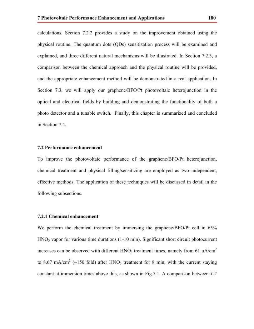
7 Photovoltaic Performance Enhancement and Applications 180
calculations. Section 7.2.2 provides a study on the improvement obtained using the
physical routine. The quantum dots (QDs) sensitization process will be examined and
explained, and three different natural mechanisms will be illustrated. In Section 7.2.3, a
comparison between the chemical approach and the physical routine will be provided,
and the appropriate enhancement method will be demonstrated in a real application. In
Section 7.3, we will apply our graphene/BFO/Pt photovoltaic heterojunction in the
optical and electrical fields by building and demonstrating the functionality of both a
photo detector and a tunable switch. Finally, this chapter is summarized and concluded
in Section 7.4.
7.2 Performance enhancement
To improve the photovoltaic performance of the graphene/BFO/Pt heterojunction,
chemical treatment and physical filling/sensitizing are employed as two independent,
effective methods. The application of these techniques will be discussed in detail in the
following subsections.
7.2.1 Chemical enhancement
We perform the chemical treatment by immersing the graphene/BFO/Pt cell in 65%
HNO3 vapor for various time durations (1-10 min). Significant short circuit photocurrent
increases can be observed with different HNO3 treatment times, namely from 61 μA/cm2
to 8.67 mA/cm2 (~150 fold) after HNO3 treatment for 8 min, with the current staying
constant at immersion times above this, as shown in Fig.7.1. A comparison between J-V
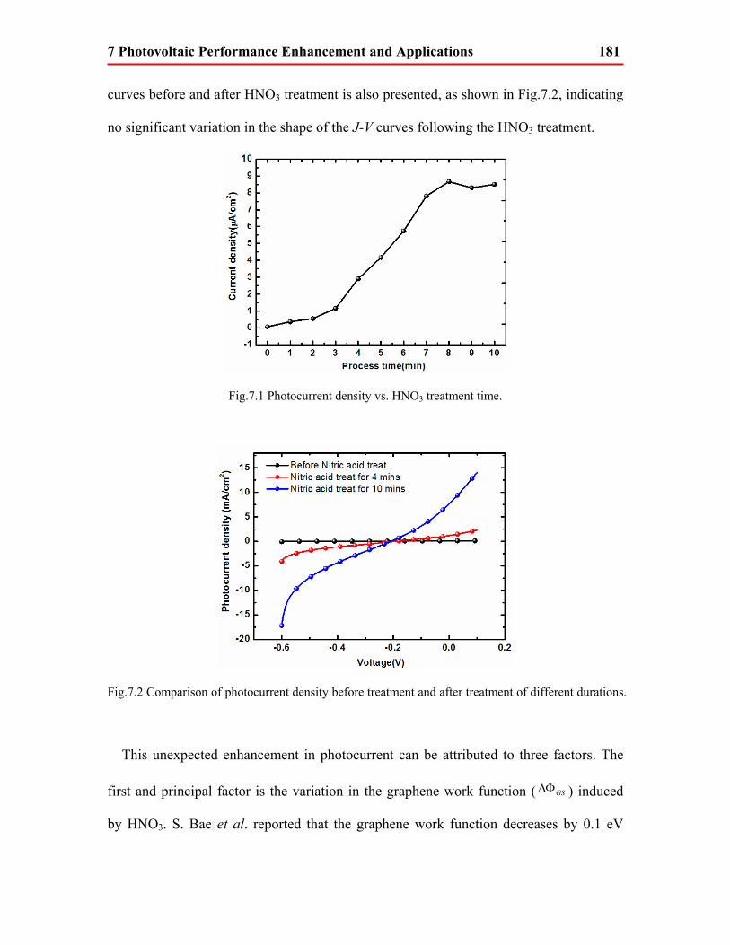
7 Photovoltaic Performance Enhancement and Applications 181
curves before and after HNO3 treatment is also presented, as shown in Fig.7.2, indicating
no significant variation in the shape of the J-V curves following the HNO3 treatment.
Fig.7.1 Photocurrent density vs. HNO3 treatment time.
Fig.7.2 Comparison of photocurrent density before treatment and after treatment of different durations.
This unexpected enhancement in photocurrent can be attributed to three factors. The
first and principal factor is the variation in the graphene work function ( GSΔΦ ) induced
by HNO3. S. Bae et al. reported that the graphene work function decreases by 0.1 eV
7 Photovoltaic Performance Enhancement and Applications 182
during HNO3 treatment [220]. As discussed in Section 6.4, the photocurrent density term
is proportional to /B Bq K Te− Φ , as indicated in the calculation below. The current density
ratio with and without HNO3 treatment is expressed as:
// ~ B Bq K Tafter beforej j e− ΔΦ
~ 144; (7.1)
which exhibits a good agreement with our experimental results. Second, the sheet
resistance of the graphene top electrode can also be affected by HNO3 treatment. As
explained by S. Bae et al. [220], the electrons in the graphene sheet can be withdrawn due
to the strong oxidation property of HNO3 and the graphene sheet can thus be regarded as
p-doped during the HNO3 treatment. The p-doping during the redox process will increase
the carrier concentration in the graphene sheet can reduce the sheet resistance according
to the following expression:
1( )n pe n p
ρμ μ
=+ , (7.2)
where ρ is the resistivity and μ is the mobility of the graphene sheet. The graphene
essheet r istance for different HNO3 treatment times is shown in Fig.7.3, and is in
agreement with our analysis [204,228]. The third factor in the photocurrent enhancement
is that the impurities and remanent graphene/BFO interface state can also be removed
during the redox process thus improving the electrical properties of the contact [208].

7 Photovoltaic Performance Enhancement and Applications 183
Fig.7.3 Graphene sheet resistance for different HNO3 treatment times.
7.2.2 Physical enhancement
On the other hand, we perform the physical filling routine by dipping CdSe QDs (2.5
mg/mL, exciton peak at 530 nm) in the graphene/BFO/Pt heterojunction. A high
resolution TEM image, shown in Fig.7.4, demonstrates the random distribution of the
CdSe QDs nanocrystallite. The inset of Fig.7.4 provides a colour photograph of the CdSe
QDs solution. The short circuit photocurrent demonstrate a ~5 fold increase, namely from
61 μA/cm2 to 0.32 mA/cm2, after CdSe QDs filling, as presented in Fig.7.5.
7 Photovoltaic Performance Enhancement and Applications 184
Fig.7.4 High resolution TEM image of CdSe QDs, exhibiting a random nanocrystallite distribution;
the inset is a colour photograph of the CdSe QDs solution.
Fig.7.5. Photocurrent density variation before and after QDs filling/sensitizing.
Unlike the variation in the graphene work function caused by the chemical treatment,
the photovoltaic improvement seen here can be attributed to the enhancement in the
photon absorption and exciton transfer process. Since the CdSe QDs possess a small band
gap (~ 1.70 eV) [229] and wide absorption band, the introduction of CdSe QDs to
graphene/BFO/Pt will help absorb photons with energy less than the BFO band gap. The
usage of CdSe QDs is therefore equivalent to adding an intermediate energy level to the
graphene/BFO/Pt heterojunction band diagram and helps to harvest the incident photons
with lower energy, and enlarge the absorption band of the BFO material, as illustrated in
Fig.7.6.
7 Photovoltaic Performance Enhancement and Applications 185
Fig.7.6 BFO absorption variation before and after QDs sensitization.
As an electron supplier and transporter, QDs can provide an ultra-high electron
injection rate of ~1010 s-1 into the BFO crystal [230], and correspondingly the holes are
scavenged by a redox coupling process, as depicted schematically in Fig.7.7. Such a high
exciton transportation rate will minimize the possibility of recombination and thus
increase the photovoltaic performance. On the other hand, the graphene electrode with a
large surface area, high aspect ratio, and high carrier mobility, also plays a role as an
electron donor to the QDs in the carrier transportation and collection process.
Furthermore, a multiple exciton generation (MEG) effect reported in QDs can also
contribute to this photovoltaic enhancement [231,232]. With QDs, more than one
electron-hole pair can be stimulated by one “high energy” incident photon [233,234],
resulting in conversion quantum efficiency greater than 100%. As reported by R. J.
Ellingson and R. D. Schaller et al. [232,235], three electron-hole pairs can be stimulated
by a photon for which the energy is four times that of the QDs band gap, and the number
of excitons can reach up to seven if the photon energy increases to eight times that of the
7 Photovoltaic Performance Enhancement and Applications 186
QDs band gap. Such unique properties of QDs can redouble the photo generated carriers
under the same illumination and thus increases the conversion efficiency in an application.
Fig.7.7 Schematic illustration of the redox and electron transfer process with QDs filling/sensitizing.
7.2.3 Comparison of chemical and physical enhancements
The chemical and physical routines both have their advantages and drawbacks in terms of
improving the photovoltaic performance of the graphene/BFO/Pt heterojunction. Both
routines are easy to implement and can provide obvious enhancement in the photocurrent.
HNO3 treatment is economical and can offer a large improvement in photocurrent (~150
fold); however, the strong oxidizability may damage not only the graphene electrode but
also the adjacent electrical components in an integrated application. On the other hand,
due to the redox nature of the chemical treatment, the improved photocurrent could
degrade over long-term operation, resulting in instability in an application. The method
using inorganic QDs filling/sensitizing is damage-free to the solar cell and can provide
long-term functionality and stability. Also, as an “artificial atom”, the band gap of the
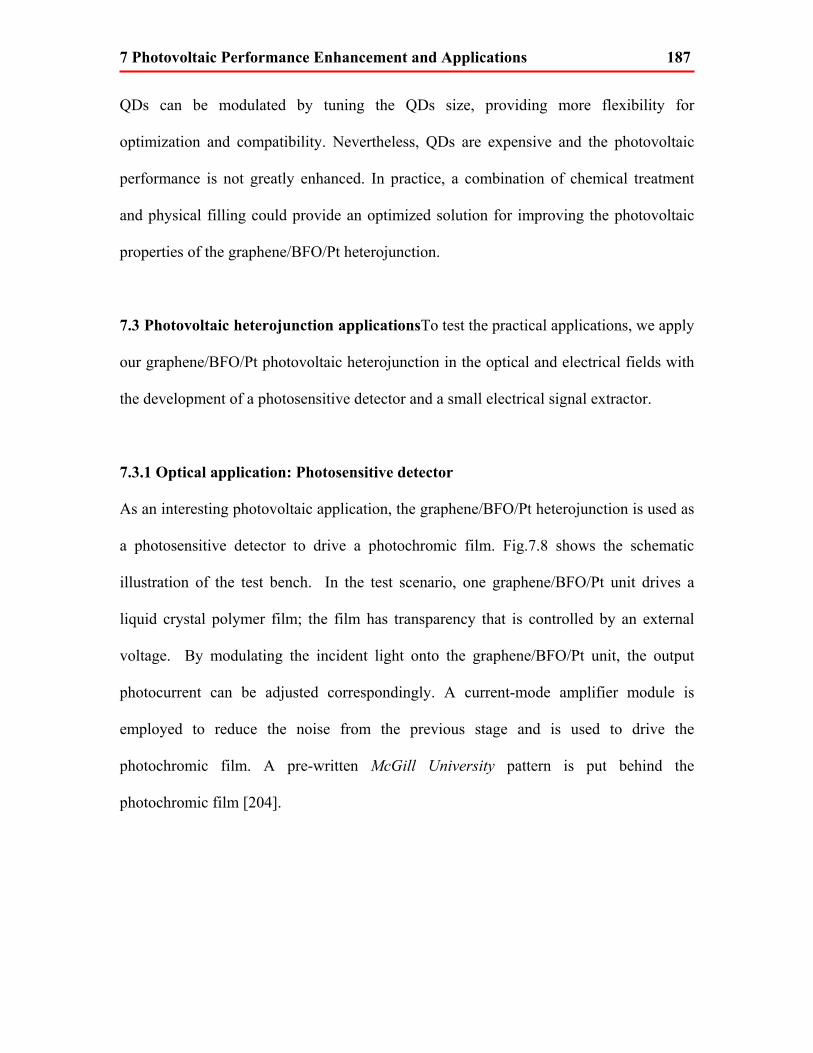
7 Photovoltaic Performance Enhancement and Applications 187
QDs can be modulated by tuning the QDs size, providing more flexibility for
optimization and compatibility. Nevertheless, QDs are expensive and the photovoltaic
performance is not greatly enhanced. In practice, a combination of chemical treatment
and physical filling could provide an optimized solution for improving the photovoltaic
properties of the graphene/BFO/Pt heterojunction.
7.3 Photovoltaic heterojunction applicationsTo test the practical applications, we apply
our graphene/BFO/Pt photovoltaic heterojunction in the optical and electrical fields with
the development of a photosensitive detector and a small electrical signal extractor.
7.3.1 Optical application: Photosensitive detector
As an interesting photovoltaic application, the graphene/BFO/Pt heterojunction is used as
a photosensitive detector to drive a photochromic film. Fig.7.8 shows the schematic
illustration of the test bench. In the test scenario, one graphene/BFO/Pt unit drives a
liquid crystal polymer film; the film has transparency that is controlled by an external
voltage. By modulating the incident light onto the graphene/BFO/Pt unit, the output
photocurrent can be adjusted correspondingly. A current-mode amplifier module is
employed to reduce the noise from the previous stage and is used to drive the
photochromic film. A pre-written McGill University pattern is put behind the
photochromic film [204].
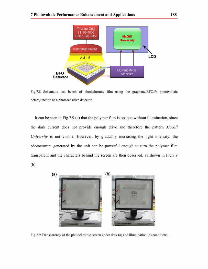
7 Photovoltaic Performance Enhancement and Applications 188
Fig.7.8 Schematic test bench of photochromic film using the graphene/BFO/Pt photovoltaic
heterojunction as a photosensitive detector.
It can be seen in Fig.7.9 (a) that the polymer film is opaque without illumination, since
the dark current does not provide enough drive and therefore the pattern McGill
University is not visible. However, by gradually increasing the light intensity, the
photocurrent generated by the unit can be powerful enough to turn the polymer film
transparent and the characters behind the screen are then observed, as shown in Fig.7.9
(b).
Fig.7.9 Transparency of the photochromic screen under dark (a) and illumination (b) conditions.

7 Photovoltaic Performance Enhancement and Applications 189
7.3.2 Electrical application: Tunable switch
Our graphene/BFO/Pt photovoltaic heterojunction can be used as a bidirectional tunable
switch. In the dark J-V curve, as shown in Fig.7.10, it can be seen that the
graphene/BFO/Pt heterojunction exhibits a bidirectional shoot-through characteristic with
a rectifying window of 3.13 V. Large signals beyond the threshold voltages (-1.49 and
+1.64 V) can pass through the switch while others will be rectified.
Fig.7.10 Dark/light photocurrent density and corresponding rectifying window of the
graphene/BFO/Pt photovoltaic heterojunction.
Such a bidirectional switchable property can be attributed to the intrinsic ferroelectric
nature of the BFO material. The rectifying window can be modulated by illumination or
by heating; it changes from 3.13 to 1.98 V by applying illumination, as shown in Fig.7.10.
Experiments are performed to confirm this bidirectional switchable property. Fig.7.11(a)
shows the application test bench and Fig.7.11 (b)-(c) show the output current with
rectangular pulse signals with different amplitudes (3 and 0.5 V, peak value). A clear
rectifying effect can be found in the 0.5 V input pattern (Fig.7.11(c)), while a good
conduction property can be observed with the 3 V signal (Fig.7.11 (b), the graded rise-

7 Photovoltaic Performance Enhancement and Applications 190
falling-edge is due to the charging-discharging effect caused by the junction capacitance).
Moreover, a sweep in voltage from -3 to 3 V with increments of 0.1 V and time duration
of 100 ms is applied to the heterojunction. A good rectifying response is also found
(Fig.7.11(d)), indicating a rectifying effect in both digital and analog applications. The
simple device structure (sandwich structure), easy fabrication process (sol-gel), tunable
rectifying window (illumination and heat), and easy integration are the major advantages
of the graphene/BFO/Pt-based bidirectional switch compared with traditional
bidirectional switches composed using different circuit elements.
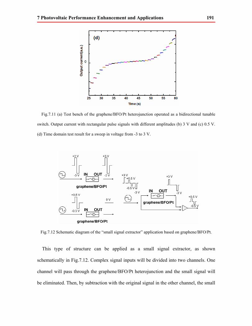
7 Photovoltaic Performance Enhancement and Applications 191
Fig.7.11 (a) Test bench of the graphene/BFO/Pt heterojunction operated as a bidirectional tunable
switch. Output current with rectangular pulse signals with different amplitudes (b) 3 V and (c) 0.5 V.
(d) Time domain test result for a sweep in voltage from -3 to 3 V.
Fig.7.12 Schematic diagram of the “small signal extractor” application based on graphene/BFO/Pt.
This type of structure can be applied as a small signal extractor, as shown
schematically in Fig.7.12. Complex signal inputs will be divided into two channels. One
channel will pass through the graphene/BFO/Pt heterojunction and the small signal will
be eliminated. Then, by subtraction with the original signal in the other channel, the small

7 Photovoltaic Performance Enhancement and Applications 192
signal will be separated from the large signal. Such a small signal extractor is desirable in
fields where the signal to noise ratio is fairly low.
7.4 Conclusion
In this chapter, we advanced our photovoltaic investigation of the graphene/BFO/Pt
heterojunction and studied the performance enhancement and optimization processes. To
start with, we investigated the chemical enhancement effect. By introducing HNO3 to the
photovoltaic heterojunction, a ~150 fold improvement in photocurrent was observed in
our study. This dramatic enhancement effect was then explained in detail using our
theoretical model built in Chapter 6. A physical enhancement approach, CdSe QDs
sensitization and filling, was used in the graphene/BFO/Pt heterojunction, and the
corresponding performance enhancement was reported experimentally and theoretically.
As a conclusion, the advantages and disadvantages of both chemical and physical
routines were compared. In the second part of this chapter, we applied our
graphene/BFO/Pt photovoltaic unit in the electrical and optical fields. A photosensitive
detector and a tunable switch were proposed and implemented in our study.
8 Conclusion 193
Chapter 8
Conclusion
F
erroelectric materials have attracted significant research interest due to their
unique electrical, optical, dielectric, piezoelectric, and photovoltaic properties.
The coupling of such properties provides extra degrees of freedom in many
technologically demanding applications, for instance, non-volatile ferroelectric random
access memory (FeRAM), optical waveguides and modulators, high-K mediums,
piezoelectric sensors and varactors, and photovoltaic devices. As an important application
format, ferroelectric thin films have been extensively investigated since the late 1960s,
when silicon integration processes and thin film deposition technologies began to boom.
Research regarding theoretical ferroelectric principles, materials engineering, and
fabrication technologies is always active in ferroelectric related fields. The research
presented in this thesis provides a comprehensive investigation, including theoretical
principles, fabrication technology, performance optimization, and electrical/optical
application of two novel ferroelectric materials, namely, Nd-doped bismuth titanate
(BNdT) and bismuth ferrite (BFO). In this chapter, we provide a summary of the work
presented in this thesis. We also reiterate the central ideas and research methodologies
associated with this work. Finally, we suggest directions for future work and other

8 Conclusion 194
research avenues that may be pursued.
8.1 Summary
In Chapter 1, we provided motivation for the research presented in this thesis, and briefly
introduced ferroelectric based electrical, optical, and photovoltaic applications. By
detailing the current problem statement in the three major ferroelectric application
domains, we outlined the research objectives that demarcate the course of this work. A
section listing the original contributions of this thesis was supplied, followed by a full
thesis overview.
Chapter 2 provided the background necessary for understanding ferroelectric research
and applications. We started the review with a description of the ferroelectric mechanism,
fabrication technologies, and the development of ferroelectric materials. We then
introduced current state of the art research in the ferroelectric based electrical, optical,
and photovoltaic domains.
In Chapter 3, we presented fabrication and characterization of the ferroelectric material
BNdT. Starting with the precursor preparation, we studied the sol-gel and spinning
coating processes for the BNdT material. Different fabrication parameters were analyzed
in order to optimize the ferroelectric properties of the BNdT material. Microstructure
properties such as XRD, Raman scattering, SEM, AFM, TEM, etc., were also
investigated. Different ferroelectric performance characteristics, such as remnant
polarization, fatigue endurance, and leakage density were provided in detail. In the latter
part of this chapter, material engineering was applied to fabricate BNdT materials with

8 Conclusion 195
different elemental constituents, and the corresponding variation in properties was therein
reported.
Based on our studies up to this point, we furthered our research into the optical
characterization of BNdT in Chapter 4, and demonstrated the first systematic
investigation of BNdT optical properties. With different fabrication parameters and
elemental constituents, optical parameters such as optical transmittance, refractive index,
extinction coefficient, and optical band gap energy were examined and their correlation
with different fabrication parameters and the microstructure were investigated both
experimentally and theoretically.
Chapter 5 presented the ferroelectric characterization of a multiferroic BFO material.
Due to the intrinsic low conductivity at room temperature, the ferroelectric performance
of the pure BFO material has never been reported. Based on the content discussed in
Chapters 2 and 3, we employed the BNdT ferroelectric thin film as a seeding layer for the
BFO/BNdT multilayer heterojunction, and we report the room temperature ferroelectric
measurement of this pure BFO ferroelectric for the first time. A theoretical analysis was
conducted to describe the phenomenon of ferroelectric enhancement, and a ferroelectric
inducing effect was presented and discussed.
In Chapter 6, photovoltaic research on the multiferroic BFO material was presented as
an advanced topic of investigation on BFO ferroelectrics. By introducing a graphene
nano transparent electrode, we reported enhanced photovoltaic performance of the BFO
material in a graphene/polycrystalline BFO/Pt heterojunction structure for the first time.
The remarkable electrical and optical properties of the graphene sheet, including ballistic
electronic transport, ultra high carrier mobility, high conductivity and transparency, result
8 Conclusion 196
in a superior BFO photovoltaic performance which is much improved compared to results
reported in the literature. A theoretical model considering the ferroelectric polarization,
interface states, and energy band bending effect, were proposed to describe the BFO
ferroelectric photovoltaic effect and carrier transport behaviour for the first time.
Important photovoltaic parameters, such as conversion efficiency, illumination intensity
response, ON/OFF characteristics, minority carrier lifetime, and external quantum
efficiency (EQE), were investigated experimentally and theoretically.
Chapter 7 investigated optimization of the existing photovoltaic effect in the
graphene/polycrystalline BFO/Pt heterojunction. HNO3 treatment and CdSe quantum
dots (QDs) filling/sensitizing, as two independent chemical and physical routines, were
processed and compared. The photocurrent density demonstrated a significant
improvement of ~150 fold after HNO3 treatment, while a considerable enhancement of
~5 fold was seen with QDs filling/sensitizing. Finally, a photosensitive detector and a
tunable switch were proposed as two interesting applications of the BFO photovoltaic
effect.
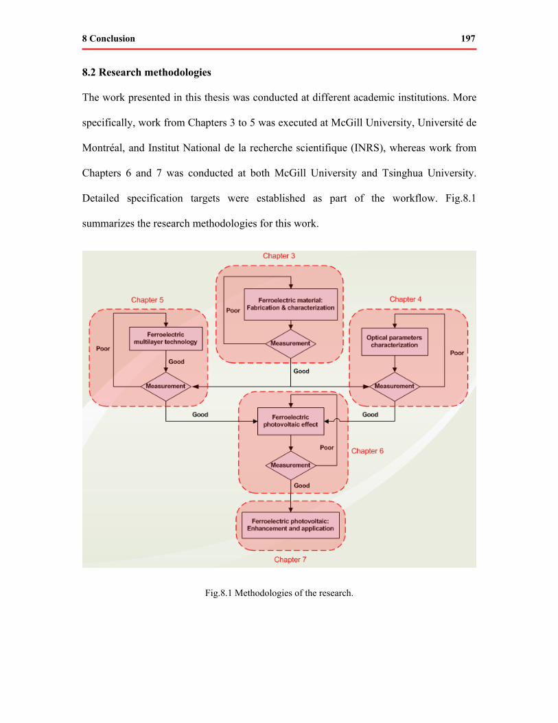
8 Conclusion 197
8.2 Research methodologies
The work presented in this thesis was conducted at different academic institutions. More
specifically, work from Chapters 3 to 5 was executed at McGill University, Université de
Montréal, and Institut National de la recherche scientifique (INRS), whereas work from
Chapters 6 and 7 was conducted at both McGill University and Tsinghua University.
Detailed specification targets were established as part of the workflow. Fig.8.1
summarizes the research methodologies for this work.
Fig.8.1 Methodologies of the research.

8 Conclusion 198
8.3 Future research avenues
Although the objectives of this research have been fulfilled, there are still other research
opportunities left to be investigated. Below, we propose directions for future research that
could follow from the work presented in this thesis.
(1) Preparation of the BNdT material
As a novel ferroelectric material, BNdT has attracted much interest since its discovery.
However, to the best of our knowledge, all of the research has been conducted based on
sol-gel derived BNdT thin films; a physical routine for preparing the BNdT material has
never been reported. According to common practice, a ferroelectric thin film derived
using a physical routine will possess better ferroelectric phase and thus better
performance in a ferroelectric application. Epitaxial growth, for instance, may be a good
practice, since it can help minimize the grain boundaries existing in polycrystalline phase,
and thus reduces the light scattering in optical applications. Meanwhile, due to its unique
3D deposition feature, the MOCVD routine may also be a useful way of preparing the
BNdT material, especially in some 3D MEMS related applications.
(2) Optical application of the BNdT material
Few research reports have been published on the topic of optical applications of BNdT
material; most of the existing research has focused on electrical related applications. The
content presented in this thesis provides a valuable advancement in the study of BNdT in
the optical domain. Optical waveguides, modulators, and switches would be interesting
applications that could be investigated in the near future.
(3) Thick film technology in ferroelectric optical MEMS
As discussed in this thesis, the ferroelectric based actuator is a promising candidate in

8 Conclusion 199
today’s optical MEMS domain. However, the thickness of the ferroelectric film is an
important fabrication issue to consider in the design and application. Ferroelectric thin
films, as applied in electrical applications such as FeRAM, cannot provide sufficient
driving force for scanning mirrors. For example, for the PZT material, a thickness of
more than 1 μm is required to achieve sufficient force to actuate the mirrors. Many
fabrication processes such as screen printing sol-gel, hydrothermal, and gas deposition
have been investigated in attempts to improve the thickness of the as-prepared PZT film.
However, very few of these methods have met the high deposition rate, low process
temperature, large area coverage, and cost requirements. Many approaches to increase the
deposition rate of the ferroelectric thick film in optical MEMS applications are still being
researched.
(4) The operating principle of ferroelectric EO devices
Due to the complex nature of the frequency response of the EO effect in ferroelectric
materials, the operating principle of ferroelectric EO devices is not well understood, and
no explicit models describing the dynamic EO response have been demonstrated. To
further establish the use of ferroelectric materials in high-bandwidth applications, it is
necessary to first determine an accurate model for the ferroelectric dynamic EO response.
Recently, domain reorientation has been proven to be a primary mechanism responsible
for the transient, nonlinear optical response of ferroelectric materials at steady state.
However, the simultaneous response of the ferroelectric EO effect has not yet been
reported, and related studies are necessary to further develop ferroelectric EO research.

8 Conclusion 200

9 References 201
References
[1] M. E. Lines and A.M.Glass, Principles and applications of ferroelectrics and related materials. Oxford: Clarendon Press, 1977.
[2] J. Valasek, “Piezo-Electric and Allied Phenomena in Rochelle Salt,” Phys. Rev., vol. 17, no. 4, pp. 475-481, 1921.
[3] J. Wang, J. B. Neaton, H. Zheng, V. Nagarajan, S. B. Ogale, B. Liu, D. Viehland, V. Vaithyanathan, D. G. Schlom, U. V. Waghmare, N. A. Spaldin, K. M. Rabe, M. Wuttig, and R. Ramesh, “Epitaxial BiFeO3 Multiferroic Thin Film Heterostructures,” Science, vol. 299, no. 5613, pp. 1719-1722, 2003.
[4] H. Adachi and K. Wasa, “Sputtering preparation of ferroelectric PLZT thin films and their optical applications,” IEEE Trans. Ultrason. Ferroelectr. Freq. Control., vol. 38, no. 6, pp. 645-655, 1991.
[5] S. V. Kalinin, A. N. Morozovska, L. Q. Chen, and B. J. Rodriguez, “Local polarization dynamics in ferroelectric materials,” Rep. Prog. Phys., vol. 73, no. 5, pp. 056502 (67 pages), 2010.
[6] L. E. Cross, “Ferroelectricmaterials for electromechanical transducer applications,” Mater. Chem. Phys., vol. 43, no. 2, pp. 108-115, 1996.
[7] S. Tehrani, E. Chen, M. Durlam, M. DeHerrera, J. M. Slaughter, J. Shi, and G. Kerszykowski, “High density submicron magnetoresistive random access memory (invited),” J. Appl. Phys., vol. 85, no. 8, pp. 369931 (6 pages), 1999.
[8] S. Trolier-McKinstry and P. Muralt, Electroceramic-Based MEMS: Fabrication-Technology and Applications, New York: Springer, 2005.
[9] M. J. Lancaster, J. Powell, and A. Porch, “Thin-film ferroelectric microwave devices,” Supercond. Sci. Technol., vol. 11, no. 11, pp. 1323-1334, 1998.
[10] G. E. Moore, “Cramming More Components onto Integrated Circuits,” Electronics, vol. 38, no. 8, pp. 114-117, 1965.
[11] S. S. Eaton, D. B. Butler, M. Parris, D. Wilson, and H. McNeillie, “A ferroelectric nonvolatile memory” Dig.Tech. Pap.-IEEE Int. Solid-State Circuits Conf. vol. 130, pp. 329, 1988.
[12] N. Setter, D. Damjanovic, L. Eng, G. Fox, S. Gevorgian, S. Hong, A. Kingon, H. Kohlstedt, N. Y. Park, G. B. Stephenson, I. Stolitchnov, A. K. Taganstev, D. V. Taylor, T. Yamada, and S. Streiffer, “Ferroelectric thin films: Review of materials, properties, and applications,” J. Appl. Phys., vol. 100, no. 5, pp. 051606 (46 pages), 2006.
[13] K. M. Lakin and J. S. Wang, “Acoustic bulk wave composite resonators,” Appl. Phys. Lett., vol. 38, no. 3, pp. 125 (3 pages), 1981.
[14] K. M. Lakin, G. R. Kline, and K. T. McCarron, “Development of miniature filters for wireless applications,” IEEE Trans. Microwave Theory Tech., vol. 43, no. 12, pp. 2933-2939, 1995.
[15] A. B. Ustinov, B. A. Kalinikos, V. S. Tiberkevich, A. N. Slavin, and G. Srinivasan, “Q factor of dual-tunable microwave resonators based on yttrium iron garnet and barium strontium titanate layered structures,” Appl. Phys. Lett., vol. 103, no. 6, pp. 063908 (3 pages), 2008.
9 References 202
[16] S. Courrèges, B. Lacroix, A. Amadjikpe, S. Phillips, Z. Y. Zhao, K. Choi, A. Hunt, and J. Papapolymerou, “Back-to-Back Tunable Ferroelectric Resonator Filters on Flexible Organic Substrates,” IEEE Trans. Ultrason. Ferroelectr. Freq. Control, vol. 57, no. 6, pp. 1267-1275, 2010.
[17] A. Vorobiev, P. Rundqvist, K. Khamchane1, and S. Gevorgian, “Silicon substrate integrated high Q-factor parallel-plate ferroelectric varactors for microwave/millimeterwave applications,” Appl. Phys. Lett., vol. 83, no. 15, pp. 3144 (3 pages), 2003.
[18] J. A. Thomas and Y .Fainman, “Optimal Cascade Operation of Optical Phased-Array Beam Deflectors,” Appl. Opt., vol. 37, no. 26, pp. 6196–6212, 1998.
[19] Q. Ye, Z. Dong, R. Qu and Z. Fang, “Experimental investigation of optical beam deflection based on PLZT electro-optic ceramic,” Opt. Express, vol. 15, no. 25, pp. 16933–16944, 2007.
[20] D. K. Fork, F. Armani-Leplingard, J.J. Kingston, “Thin Film Epitaxial Oxide Optical Waveguides,” MRS Bull., vol. 392, no. 189, pp. 53–58, 1996.
[21] T. Choi, S. Lee, Y. J. Choi, V. Kiryukhin, and S. W. Cheong, “Switchable Ferroelectric Diode and Photovoltaic Effect in BiFeO3,” Science, vol. 324, no. 5923, pp. 63-66, 2009.
[22] S. Y. Yang, J. Seidel, S. J. Byrnes, P. Shafer, C.-H. Yang, M. D. Rossell, P. Yu, Y.-H. Chu, J. F. Scott, J. W. Ager III, L. W. Martin, and R. Ramesh, “Above-bandgap voltages from ferroelectric photovoltaic devices,” Nat. Nanotechnol., vol. 5, pp. 143-147, 2010.
[23] S. Y. Yang, L. W. Martin, S. J. Byrnes, T. E. Conry, S. R. Basu, D. Paran, L. Reichertz, J. Ihlefeld, C. Adamo, A. Melville, Y.-H. Chu, C.-H. Yang, J. L. Musfeldt, D. G. Schlom, J. W. Ager, III, and R. Ramesh, “Photovoltaic effects in BiFeO3,” Appl. Phys. Lett., vol. 95, no. 6, pp. 062909 (3 pages), 2009.
[24] H. T. Huang, “Solar energy: Ferroelectric photovoltaics,” Nat. Photonics, vol. 4, pp. 134-135, 2010.
[25] V. Garcia, M. Bibes, L. Bocher, S. Valencia, F. Kronast, A. Crassous, X. Moya, S. Enouz-Vedrenne, A. Gloter, D. Imhoff, C. Deranlot, N. D. Mathur, S. Fusil, K. Bouzehouane, and A. Barthélémy, “Ferroelectric Control of Spin Polarization,” Science, vol. 327, no. 5969, pp. 1106-1110, 2010.
[26] H. D. Megaw, “Crystal Structure of Barium Titanate,” Nature, vol. 155, pp. 484, 1945.
[27] Y. Ivry, D. P. Chu, J. F. Scott, and C. Durkan, “Flux Closure Vortexlike Domain Structures in Ferroelectric Thin Films,” Phys. Rev. Lett., vol. 104, no. 20, pp. 207602 (4 pages), 2010.
[28] X. Hong, A. Posadas, K. Zou, C. H. Ahn, and J. Zhu, “High-Mobility Few-Layer Graphene Field Effect Transistors Fabricated on Epitaxial Ferroelectric Gate Oxides,” Phys. Rev. Lett., vol. 102, no. 13, pp. 207602 (4 pages), 2009.
[29] B. T. Liu, J. W. Zhao, X. H. Li, Y. Zhou, F. Bian, X. Y. Wang, Q. X. Zhao, Y. L. Wang, Q. L. Guo, L. X. Wang, and X. Y. Zhang, “Enhanced dielectric constant and fatigue-resistance of PbZr0.4Ti0.6O3 capacitor with magnetic intermetallic FePt top electrode,” Appl. Phys. Lett., vol. 96, no. 25, pp. 252904 (3 pages), 2010.
[30] A. K. Dikshit, M. Pal, P. Biswas, and S. K. Bhadra, “Efficient Lasing Wavelength Tuning in Distributed Bragg Reflector Fiber Laser Using PZT Macrofiber Composite Actuator,” J. Lightwave Technol., vol. 28, no. 12, pp. 1783-1788, 2010.
[31] S. Masuda, A. Seki, and Y. Masuda, “Influence of crystal phases on electro-optic properties of epitaxially grown lanthanum-modified lead zirconate titanate films,” Appl. Phys. Lett., vol. 96, no. 7, pp. 072901 (3 pages), 2010.
[32] F. Chen, Q. Z. Liu, H. F. Wang, F. H. Zhang, and W. B. Wu, “Polarization switching and fatigue in Pb(Zr0.52Ti0.48)O3 films sandwiched by oxide electrodes with different carrier types,” Appl. Phys. Lett., vol. 90, no. 19, pp. 192907 (3 pages), 2007.
9 References 203
[33] X. F. Du and I. W. Chen, “Fatigue of Pb(Zr0.53Ti0.47)O3 ferroelectric thin films,” J. Appl. Phys., vol. 83, no. 12, pp. 7789 (10 pages), 1998.
[34] U. Chon, H. M. Jang, M. G. Kim, and C. H. Chang, “Layered Perovskites with Giant Spontaneous Polarizations for Nonvolatile Memories,” Phys. Rev. Lett., vol. 89, no. 8, pp. 087601 (4 pages), 2002.
[35] Y. J. Qi, X. Xiao, C. J. Lu, X. Y. Mao, and X. B. Chen, “Microstructural, ferroelectric, and dielectric properties of Bi3.15Nd0.85Ti3O12 ceramics,” J. Appl. Phys., vol. 98, no. 9, pp. 094101 (5 pages), 2005.
[36] D. Xie, Z. G. Zhang, T. L. Ren, T. Z. Liu, Y. Q. Dong, L. T. Liu, “Neodymium-doped Bi4Ti3O12 thin films for ferroelectric random access memory,” Integr. Ferroelectr., vol. 84, no. 1, pp. 67-73, 2006.
[37] Y. Y. Zang, D. Xie, Y. H. Xiao, Y. Ruan, T. L. Ren, L. T. Liu, “Microstructure and dielectric properties of Nd-doped bismuth titanate,” Integr. Ferroelectr., vol. 98, no. 1, pp. 97-104, 2008.
[38] Y. M. Chen, R. J. Zhang, Y. X. Zheng, P. H. Mao, W. J. Lu, L. Y. Chen, “Study of the Optical Properties of Bi3.15Nd0.85Ti3O12 Ferroelectric Thin Films,” J. Korean Phys. Soc., vol. 53, pp. 2299-2302, 2008.
[39] S. K. Singh, H. Ishiwara, and K. Maruyama, “Room temperature ferroelectric properties of Mn-substituted BiFeO3 thin films deposited on Pt electrodes using chemical solution deposition,” Appl. Phys. Lett., vol. 88, no. 26, pp. 262908 (3 pages), 2006.
[40] D. Lee, M. G. Kim, S. Ryu, H. M. Jang, and S. G. Lee, “Epitaxially grown La-modified BiFeO3 magnetoferroelectric thin films,” Appl. Phys. Lett., vol. 86, no. 22, pp. 222903 (3 pages), 2005.
[41] S. K. Singh and H. Ishiwara, “Doping Effect of Rare-Earth Ions on Electrical Properties of BiFeO3 Thin Films Fabricated by Chemical Solution Deposition,” Jpn. J. Appl. Phys., vol. 45, pp. 3194-3197, 2006.
[42] S. K. Singh, H. Ishiwara, K. Sato, and K. Maruyama, “Microstructure and frequency dependent electrical properties of Mn-substituted BiFeO3 thin films,” J. Appl. Phys., vol. 102, no. 9, pp. 094109 (5 pages), 2007.
[43] C. F. Chung, J. P. Lin, and J. M. Wu, “Influence of Mn and Nb dopants on electric properties of chemical-solution-deposited BiFeO3 films,” Appl. Phys. Lett., vol. 88, no. 24, pp. 242909 (3 pages), 2006.
[44] W. Ji, K. Yao and Y. C. Liang, “Bulk Photovoltaic Effect at Visible Wavelength in Epitaxial Ferroelectric BiFeO3 Thin Films,” Adv. Mater., vol. 22, no. 15, pp. 1763-1766, 2010.
[45] B. Chen, M. Li, Y. W. Liu, Z. H. Zuo, F. Zhuge, Q. F. Zhan and R. W. Li, “Effect of top electrodes on photovoltaic properties of polycrystalline BiFeO3 based thin film capacitors,” Nanotechnology, vol. 22, pp. 195201 (5 pages), 2011.
[46] T. L. Qu, Y. G. Zhao, D. Xie, J. P. Shi, Q. P. Chen and T. L. Ren, “Resistance switching and white-light photovoltaic effects in BiFeO3/Nb–SrTiO3 heterojunctions,” Appl. Phys. Lett., vol. 98, no. 17, pp. 173507 (3 pages), 2011.
[47] M. Dawber, K. M. Rabe, and J. F. Scott, “Physics of thin-film ferroelectric oxides,” Rev. Mod. Phys., vol. 77, no. 4, pp. 1083-1130, 2005.
[48] A. Kingon, P. Muralt, N. Setter, and R. Waser, Ceramic Materials for Electronics, edited by R. E. Buchanan. New York: Dekker, 2004.
[49] H. M. Duiker, P. D. Beale, J. F. Scott, C. A. Paz de Araujo, B. M. Melnick, J. D. Cuchiaro, and L. D. McMillan, “Fatigue and switching in ferroelectric memories: Theory and experiment,” J. Appl. Phys., vol. 68, no. 11, pp. 5783 (9 pages), 1990.
[50] A. Stashansa , S. Serranob, and P. Medinab, “A quantum-chemical study of oxygen-vacancy defects in PbTiO3 crystals,” Physica B, vol. 381, no. 1-2, pp. 82-89, 2005.

9 References 204
[51] D. L. Polla and L. F. Francis, “Processing and Characterization of Piezoelectric Materials and Integration into Microelectromechanical Systems,” Annu. Rev. Mater. Sci., vol. 58, pp. 563-597, 1998.
[52] S. P. Alpay, I. B. Misirlioglu, A. Sharma, and Z.G. Ban, “Structural characteristics of ferroelectric phase transformations in single-domain epitaxial films,” J. Appl. Phys., vol. 95, no. 12, pp. 8118 (6 pages), 2004.
[53] C. Kittel, Introduction to Solid State Physics, New York: Wiley, 1996.
[54] L. Borntein, Numerical Data and Functional Relationships in Science and Technology, Berlin: Springer-Verlag, 1981.
[55] N. Bar-chaimab, M. Brunsteina, J. Grunbergab, and A. Seidmantma, “Variations of the dielectric constant of pzt ferroelectric ceramics with electric field,” Ferroelectr., vol. 6, no. 1, pp. 299-305, 1973.
[56] W. Cochran and A. Zia, “Structure and dynamics of perovskite-type crystals,” Phys. Status Solidi B, vol. 25, no. 1, pp. 273-283, 1968.
[57] Z. Kutnjak, J. Petzelt, and R. Blinc, “The giant electromechanical response in ferroelectric relaxors as a critical phenomenon,” Nature, vol. 441, pp. 956-959, 2006.
[58] P. K. Petrov, N. McN Alford, A. Kozyrev, M. Gaidukov, A. Altynnikov, A. Vasilevskiy, G. Konoplev, A. Tumarkin, and A. Gagarin, “Effect of ultraviolet radiation on slow-relaxation processes in ferroelectric capacitance structures,” J. Appl. Phys., vol. 107, no. 8, pp. 084102 (6 pages), 2010.
[59] X. B. Ren, “Large electric field induced strain in ferroelectric crystals by point defect mediated reversible domain switching,” Nat. Mater., vol. 3, pp. 91-94, 2004.
[60] H. Ma, B. Q. Chen, T. Sassa, L. R. Dalton, and A. K. Y. Jen, “Highly Efficient and Thermally Stable Nonlinear Optical Dendrimer for Electrooptics,” J. Am. Chem. Soc., vo. 123, no. 5, pp. 986-987, 2001.
[61] J. West, “A quantitative X-Ray Analysis of the Structure of Potassium Dihydrogen Phasphate,” Z. Kristallogr., vol. 74, pp. 306-332, 1930.
[62] X. Chen, S. Y. Xu, N. Yao, and Y. Shi, “1.6 V Nanogenerator for Mechanical Energy Harvesting Using PZT Nanofibers,” Nano Lett., vol. 10, no. 6, pp. 2133-2137, 2010.
[63] M. A. McLachlan, D. W. McComb, M. P. Ryan, A. N. Morozovska, E. A. Eliseev, E. A. Payzant, S. Jesse, K. Seal, A. P. Baddorf, S. V. Kalinin, “Ferroelectric Materials: Probing Local and Global Ferroelectric Phase Stability and Polarization Switching in Ordered Macroporous PZT,” Adv. Funct. Mater., vol. 21, no. 5, pp. 802-811, 2011.
[64] S. N. Song , Z. T. Song, B. Liu, L. C Wu, and S. L. Feng, “Ge2Sb2Te5 and PbZr0.30Ti0.70O3 composite films for application in phase change random access memory,” Mater. Lett., vol. 64, no. 3, pp.317-319, 2010.
[65] J. Choi, J. S. Kim, I. Hwang, S. Hong, I. S. Byun, S. W. Lee, S. O. Kang, and B. H. Park, “Different nonvolatile memory effects in epitaxial Pt/PbZr0.3Ti0.7O3/LSCO heterostructures,” Appl. Phys. Lett., vol. 96, no. 26, pp. 262113 (3 pages), 2010.
[66] R. G. Polcawich, J. S.Pulskamp, T. Ivanov, M. E. Zaghloul, “Development of a PZT MEMS Switch Architecture for Low-Power Digital Applications,” J. Microelectromech. Syst., vol. 20, no. 4, pp. 1032-1042, 2011.
[67] K. H. Koha, C. K. Leea, and T. Kobayashib, “A 3-D MEMS VOA using translational attenuation mechanism based on piezoelectric PZT thin film actuators,” Proc. Eng., vol. 5, pp. 613-616, 2010.
[68] T. Kobayashi and T. C. K. Leea, “Low-Voltage Driven MEMS VOA Using Torsional Attenuation Mechanism Based on Piezoelectric Beam Actuators,” IEEE Photonics Technol. Lett., vol. 22, no. 18, pp. 1355-1357, 2010.
[69] Y. Shimakawa, Y. Kubo, Y. Nakagawa, T. Kamiyama, H. Asano, and F. Izumi, “Crystal structures and ferroelectric properties of SrBi2Ta2O9 and Sr0.8Bi2.2Ta2O9,” Appl. Phys. Lett., vol. 74, no. 13,

9 References 205
pp. 1904 (3 pages), 1999.
[70] O. Auciello, A. R. Krauss, J. Im, and J. A. Schultz, “Studies of Multicomponent Oxide Films and Layered Heterostructure Growth Processes via in Situ, Time-Of Ion Scattering and Direct Recoil Spectroscopy,” Annu. Rev. Mater. Sci., vol. 28, pp. 375-396, 1998.
[71] S. R. Summerfelt, Thin Film Ferroelectric Materials and Devices, Norwell: Kluwer Academic, 1997.
[72] B. H. Park, B. S. Kang, S. D. Bu, T. W. Noh, J. Lee, W. Jo, “Lanthanum-substituted bismuth titanate for use in non-volatile memories,” Nature, vol. 401, pp. 682-684, 1999.
[73] S. Kanga, S. Parkb, K. W. Kimc, S. I. Wooa, and S. Parka, “High-throughput screening of ferroelectric materials for non-volatile random access memory using multilayer perceptrons,” Appl. Surf. Sci., vol. 254, no. 3, pp. 725-733, 2007.
[74] C. J. Lu, Y. Qiao, Y. J. Qi, X. Q. Chen, and J. S. Zhu, “Large anisotropy of ferroelectric and dielectric properties for Bi3.15Nd0.85Ti3O12 thin films deposited on Pt/Ti/SiO2/Si,” Appl. Phys. Lett., vol. 87, no. 22, pp. 222901 (3 pages), 2005.
[75] W. Eerenstein, N. D. Mathur, J. F. Scott, “Multiferroic and magnetoelectric materials,” Nature, vol. 442, pp. 759-765, 2006.
[76] M. Fiebig, “Revival of the magnetoelectric effect,” J. Phys. D, vol. 38, no. 8, pp. R123-R152, 2005.
[77] N. A. Hill, “Why Are There so Few Magnetic Ferroelectrics?” J. Phys. Chem. B vol. 104, no. 29, pp. 6694-6709, 2000.
[78] X. D. Qi, M. Wei, Y. Lin, Q. X. Jia, D. Zhi, J. H. Dho, M. G. Blamire, and J. L. M-Dirscoll, “High-resolution x-ray diffraction and transmission electron microscopy of multiferroic BiFeO3 films,” Appl. Phys. Lett., vol. 86, no. 7, pp. 071913 (3 pages), 2005.
[79] Y. P. Wang, L. Zhou, M. F. Zhang, X. Y. Chen, J. M. Liu, and Z. G.Liu, “Room-temperature saturated ferroelectric polarization in BiFeO3 ceramics synthesized by rapid liquid phase sintering,” Appl. Phys. Lett., vol. 84, no. 10, pp. 1731 (3 pages), 2004.
[80] H. Uchida, R. Ueno, H. Funakubo, and S. Koda, “Crystal structure and ferroelectric properties of rare-earth substituted BiFeO3 thin films,” J. Appl. Phys., vol. 100, no. 1, pp. 014106 (9 pages), 2006.
[81] K. W. Yun, M. Noda, and M. Okuyama, “Effects of annealing atmosphere on crystallization and electrical properties in BiFeO3 thin films by chemical solution deposition (CSD),” J. Korean Phys. Soc., vol. 42, pp. 1153-1156, 2003.
[82] M. M. Kumar, V. R. Palkar, K. Srinivas, and S. V. Suryanarayana, “Ferroelectricity in a pure BiFeO3 ceramic,” Appl. Phys. Lett., vol. 76, no. 19, pp. 2764 (3 pages), 2000.
[83] A. Srinivas, D. W. Kim, K. S. Hong, and S. V. Suryanarayana, “Observation of ferroelectromagnetic nature in rare-earth-substituted bismuth iron titanate,” Appl. Phys. Lett., vol. 83, no. 11, pp. 2217 (3 pages), 2003.
[84] X. D. Qi, J. H. Dho, R. Tomov, M. G. Blamire, and J. L. MacManus-Driscoll, “Greatly reduced leakage current and conduction mechanism in aliovalent-ion-doped BiFeO3,” Appl. Phys. Lett., vol. 86, no. 6, pp. 062903 (3 pages), 2005.
[85] Image from the internet, http://www.tcbonding.com/sputtering.html
[86] Image from the internet, http://groups.ist.utl.pt/rschwarz/rschwarzgroup_files/PLD_files/PLD_schem.jpg
[87] Image from the internet, http://www.seas.ucla.edu/prosurf/facility.htm

9 References 206
[88] A. K. Sharma, Semiconductor Memories: Technology, Testing, and Reliability, Piscataway: IEEE Press, 1997. [89] H. Ishiwara, M. Okuyama, Y. Arimoto, Ferroelecrtric Random Access Memories: Fundamentals and Applications, New York: Springer, 2004.
[90] R. C. G. Naber, C. Tanase, P. W. M. Blom, G. H. Gelinck, A. W. Marsman, F. J. Touwslager, S. Setayesh, and D. M. de Leeuw, “High-performance solution-processed polymer ferroelectric field-effect transistors,” Nat. Mater., vol. 4, pp. 243-248, 2005.
[91] I. Lazareva, Y. Koval, P. Müller, K. Müller, K. Henkel, and D. Schmeisser, “Interface screening and imprint in poly(vinylidene fluoride/trifluoroethylene) ferroelectric field effect transistors,” J. Appl. Phys., vol. 105, no. 5, pp. 054110 (5 pages), 2005.
[92] Y. Arimoto and H. Ishiwara, “Current Status of Ferroelectric Random-Access Memory,” MRS Bull., vol. 29, pp. 823-828, 2004.
[93] H. Ishiwara, “Current status of fabrication and integration of ferroelectric-gate FET's,” Mater. Res. Soc. Sympo. Proc. (Ferroelectric Thin Film VIII), vol. 596, pp. 427-436, 2000.
[94] H. Tabata, H. Tanaka, and T. Kawai, “Formation of artificial BaTiO3/SrTiO3 superlattices using pulsed laser deposition and their dielectric properties,” Appl. Phys. Lett., vol. 65, no. 15, pp. 1970 (3 pages), 1994.
[95] L. Pintilie, E. Pentia, I. Pintilie, and T. Botila, “Field effect enhanced signal-to-noise ratio in chemically deposited PbS thin films on Si3N4/n-Si substrates,” Appl. Phys. Lett., vol. 76, no. 14, pp. 1890 (3 pages), 2000.
[96] K. Yamauchi, B. Sanyal, and S. Picozzi, “Interface effects at a half-metal/ferroelectric junction,” Appl. Phys. Lett., vol. 91, no. 6, pp. 062506 (3 pages), 2007.
[97] C. J. Först, C. R. Ashman, K. Schwarz, and P. E. Blöchl, “The interface between silicon and a high-k oxide,” Nature, vol. 427, pp. 53-56, 2004.
[98] H. Kohlstedt and H. Ishiwara, Nanoelectronics and Information Technology: Advanced Electronic Materrial and Novel Devices, Weinheim: Wiley-VCH, 2002.
[99] J. P. Han, S. W. Jung, and T. P. Ma, “Ferroelectric DRAM (FEDRAM) FET with metal/SrBi2/Ta2O9/SiN/Si gate structure,” IEEE Electron Device Lett., vol. 23, no. 2, pp. 82-84, 2002.
[100] J. P. Han and T. P. Ma, “Ferroelectric-gate transistor as a capacitor-less DRAM cell (FEDRAM),” Integr. Ferroelectr., vol. 27, no. 1-4, pp. 9-18, 1999.
[101] Y. Yasuda, M. Akamatsu, M. Tani, T. Iijima, and H. Toshiyoshi, “Piezoelectric 2D-Optical Micro Scanners with PZT Thick Films,” Integr. Ferroelectr., vol. 76, no. 1, pp. 81-91, 2005.
[102] C. K. Lee, F. L. Hsiao, T. Kobayashi, K. H. Koh, P. V. Ramana, W. F. Xiang, B. Yang, C. W. Tan, and D. Pinjala, “A 1-V Operated MEMS Variable Optical Attenuator Using Piezoelectric PZT Thin-Film Actuators,” IEEE J. Sel. Top. Quantum Electron., vol. 15, no. 5, pp. 1529-1536, 2009.
[103] G. K. Fedder, R. T. Howe, T. J. K. Liu, and E. P. Quevy, “Technologies for cofabricating MEMS and electronics,” Proc. IEEE, vol. 96, no. 2, pp. 306-322, 2008.
[104] H. Schenk, P. Durr, T. Haase, D. Kunze, U. Sobe, H. Lakner, and H. Kuck, “Large deflection micromechanical scanning mirrors for linear scans and pattern generation,” IEEE J. Sel. Top. Quantum Electron., vol. 6, no. 5, pp. 715-722, 2000.
[105] H. Xie, Y. Pan, and G. K. Fedder, “A CMOS-MEMS mirror with curled hinge comb drives,” J. Microelectromech. Syst., vol. 12, no. 4, pp. 450-457, 2003.
[106] D. W. Wine, M. P. Helsel, L. Jenkins, H. Urey, and T. D. Osborn, “Performance of a Biaxial MEMS-Based Scanner for Microdisplay Applications,” Proc. of SPIE, vol. 4178, pp. 186-196, 2000.
[107] R. A. Conant, J. T. Nee, K. Y. Lau, and R. S. Muller, Solid-State Sensor and ActuatorWorkshop, South Carolina: Hilton Head, 2000.
9 References 207
[108] A. Jain, H. Qu, S. Todd, and H. Xie, “A thermal bimorph micromirror with large bi-directional and vertical actuation,” Sens. Actuators A, vol. 122, pp. 9-15, 2005.
[109] R. Maeda, J. J. Tsaur, S. H. Lee, and M. Ichiki, “Piezoelectric microactuator devices,” J. Electroceramics, vol. 12, pp. 89-100, 2004.
[110] J. Baborowski, “Microfabrication of piezoelectric MEMS,” Integr. Ferroelectr., vol. 66, pp. 3-17, 2004.
[111] S. J. Kim, Y. H. Cho, H. J. Nam, and J. U. Bu, “Piezoelectrically pushed rotational micromirrors using detached PZT actuators for wide-angle optical switch applications,” J. Micromech. Microeng., vol. 18, pp. 125022 (7 pages), 2008.
[112] X. L. Zhang, M. Belal, G. Y. Chen, Z. Q. Song, G. Brambilla, and T. P. Newson, “Compact optical microfiber phase modulator,” Opt. Lett., vol. 37, no. 3, pp. 320-322, 2012.
[113] E. Suzuki, S. Arakawa, H. Ota, “EO probe for simultaneous electric and magnetic near-field measurements using LiNbO3 with inverted domain,” IEEE Trans. Microwave Theory Tech., vol. 53, no. 2, pp. 696-701, 2005.
[114] S. H. Wemple, M. DiDomenico, and I. Camlibel, “Relationship between linear and quadratic electro-optic coefficients in LiNbO3, LiTaO3, and other oxygen-octahedra ferroelectrics based on direct measurement of spontaneous polarization,” Appl. Phys. Lett., vol. 12, no. 6, pp. 209 (3 pages), 1968.
[115] A. Kumar, S. F. Yu, and X. F. Li, “Design and analysis of a surface plasmon polariton modulator using the electro-optic effect,” Appl. Opt., vol. 48, no. 35, pp. 6600-6605, 2009.
[116] A. Petraru, J. Schubert, M. Schmid, and Ch. Buchal, “Ferroelectric BaTiO3 thin-film optical waveguide modulators,” Appl. Phys. Lett., vol. 81, no. 8, pp. 1375 (3 pages), 2002.
[117] P. S. Tang, A. L. Meier, D. J. Towner, and B. W. Wessels, “BaTiO3 thin-film waveguide modulator with a low voltage-length product at near-infrared wavelengths of 0.98 and 1.55 µm,” Opt. Lett., vol. 30, no. 3, pp. 254-256, 2005.
[118] Q. Ye, Z. Dong, R.Qu, and Z. Fang, “Experimental investigation of optical beam deflection based on PLZT electro-optic ceramic,” Opt. Express, vol. 15, no. 25, pp. 16933-16944, 2007.
[119] N. Tanaka, M. LaBuda, D. Ritums, J. Dawley, M. Raj, D. Kudzuma, “High-speed PLZT optical switches for burst and packet switching,” International Conference on Broadband Networks, vol. 2, pp. 1118-1123, 2005.
[120] D. P. Gia Russo and C. S. Kumar, “Sputtered ferroelectric thin ‐ film electro ‐ optic modulator,” Appl. Phys. Lett., vol. 23, no. 5, pp. 229 (3 pages), 1973.
[121] K. Uchiyama, A. Kasamatsu, Y. Otani, and T. Shiosaki, “Development of PLZT Thin Film Depositions for Opto-Nano Electric Applications,” Integr. Ferroelectr., vol. 84, no. 1, pp. 129-135, 2011.
[122] R. Thapliya, Y. Okano, and S. Nakamura, “Electrooptic Characteristics of Thin-Film PLZT Waveguide Using Ridge-Type Mach–Zehnder Modulator,” J. Lightwave Technol., vol. 21, no. 8, pp. 1820-1827, 2003.
[123] H. T. Yi, T. Choi, S. G. Choi, Y. S. Oh, S.-W. Cheong, “Mechanism of the Switchable Photovoltaic Effect in Ferroelectric BiFeO3,” Adv. Mater., vol. 23, no. 30, pp. 3403-3407, 2011.
[124] V. Garcia1, M. Bibes, L. Bocher, S. Valencia, F. Kronast, A. Crassous, X. Moya, S. Enouz-Vedrenne, A. Gloter, D. Imhoff, C. Deranlot, N. D. Mathur, S. Fusil1, K. Bouzehouane1, and A. Barthélémy, “Ferroelectric Control of Spin Polarization,” Science, vol. 327, no. 5969, pp. 1106-1110, 2010.
[125] C. J. Brinker and G. W. Scherer, Sol-Gel Science: The Physics and Chemistry of Sol-Gel Processing, San Diego: Academic Press, 1990.

9 References 208
[126] L. L. Hench and J. K. West, “The sol-gel process,” Chem. Rev., vol. 90, no. 1, pp. 33-72, 1990.
[127] C. J. Brinker, A. J. Hurd, P. R. Schunk, G. C. Frye, and C. S. Ashley, “Review of sol-gel thin film formation,” J. Non-Cryst. Solids, vol. 147-148, pp. 424-436, 1992.
[128] R. W. Schwartza, T. J. Boylea, S. J. Lockwooda, M. B. Sinclaira, D. Dimosa, and C. D. Buchheita, “Sol-gel processing of PZT thin films: A review of the state-of-the-art and process optimization strategies,” Integr. Ferroelectr., vol. 7, no. 1-4, pp. 259-277, 2006.
[129] J. H. Li, Y. Qiao, X. L. Liu, C. J. Nie, C. J. Lu, Z. X. Xu, S. M. Wang, N. X. Zhang, D. Xie, H. C. Yu, and J. Q. Li, “Microstructure and ferroelectric properties of sol-gel derived Bi3.15Nd0.85Ti3O12 thin films on Pt/Ti/SiO2/Si(100),” Appl. Phys. Lett., vol. 85, no. 15, pp. 3193 (3 pages), 2004.
[130] D. Wu, A. D. Li, and N. B. Ming, “Dielectric characterization of Bi3.25La0.75Ti3O12 thin films,” Appl. Phys. Lett., vol. 84, no. 22, pp. 4505 (3 pages), 2004.
[131] D. Xie, T. L. Ren, L. T. Liu, “Fabrication and Optical Properties of SrBi4Ti4O15/BaBi4Ti4O15 Graded Ferroelectric Thin Films,” Integr. Ferroelectr., vol. 68, no. 1, pp. 3-11, 2004.
[132] Y. Y. Zang, D. Xie, Y. Chen, M. H. Li, C. Chen, T. L. Ren, and D. V. Plant, “Temperature dependence of optical and structural properties of ferroelectric B3.15Nd0.85Ti3O12 thin film derived by sol–gel process,” J. Sol-Gel Sci. Technol., vol. 61, no. 1, pp. 236-242, 2012.
[133] Jang G, Kim K, and Yoon D, “Dielectric Properties of Bi3.25Nd0.75Ti3O12 Thin Film,” J. Korean Phys. Soc., vol. 45, no. 3, pp. 693-696, 2004.
[134] C. P. Luo and D. J. Sellmyer, “Structural and magnetic properties of FePt:SiO2 granular thin films,” Appl. Phys. Lett., vol. 75, no. 20, pp. 3162 (3 pages), 1999.
[135] X. Z. Ding, X. H. Liu, Y and . Z. He, “Grain size dependence of anatase-to-rutile structural transformation in gel-derived nanocrystalline titania powders,” J. Mater. Sci. Lett., vol. 15, no. 20, pp. 1789-1791, 1996.
[136] G. Catalan, J. F. Scott, “Physics and Applications of Bismuth Ferrite,” Adv. Mater., vol. 21, no. 24, pp. 2463-2485, 2009.
[137] K. Watanabe, A. J. Hartmann, R. N. Lamb, and J. F. Scott, “Electronic characteristics of the SrBi2Ta2O9–Pt junction,” J. Appl. Phys., vol. 84, no. 4, pp. 2170 (6 pages), 1998.
[138] C. D. Gutleben, “Band alignments of the platinum/SrBi2Ta2O9 interface,” Appl. Phys. Lett., vol. 71, no. 23, pp. 3444 (3 pages), 1997.
[139] T. Atsuki, N. Soyama, T. Yonezawa, and K. Ogi, “Preparation of Bi-Based Ferroelectric Thin Films by Sol-Gel Method,” Jpn. J. Appl. Phys., vol. 34, pp. 5096-5099, 1995.
[140] T. Kojima, T. Sakai, T. Watanabe, H. Funakubo, K. Saito, and M. Osada, “Large remanent polarization of (Bi,Nd)4Ti3O12 epitaxial thin films grown by metalorganic chemical vapor deposition,” Appl. Phys. Lett., vol. 80, no. 15, pp. 2746 (3 pages), 2002.
[141] X. S. Gao, J. M. Xue, and J. Wang, “Polarization behaviors of (Bi3.15Nd0.85)Ti3O12 thin films deposited by radio-frequency magnetron sputtering,” J. Appl. Phys., vol. 98, no. 10, pp. 104106 (5 pages), 2005.
[142] A. Furuya and J. D. Cuchiaro, “Compositional dependence of electrical characteristics of SrBi2(Ta1−xNbx)2O9 thin-film capacitors,” J. Appl. Phys., vol. 84, no. 12, pp. 6788 (7 pages), 1998.
[143] Y. Y. Zang, D. Xie, Y. H. Xiao, K. H. Xue, T. L. Ren, and L. T. Liu, “Preparation and characterization for B3.15Nd0.85Ti3O12 thin film by sol-gel process,” Proc. Electron Devices and Semiconductor Technology, pp. 121-124, 2007.

9 References 209
[144] H. Uchida, H. Yoshikawa, I. Okada, H. Matsuda, T. Lijima, T. Watanabe, T. Kojima, and H. Fubakubo, "Approach for enhanced polarization of polycrystalline bismuth titanate films by Nd3+/V5+ cosubstitution," Appl. Phys. Lett., vol. 81, no. 12, pp. 2229 (3 pages), 2002.
[145] D. Wu, Y. D. Xia, A. D. Li, Z. G. Liu, and N. B. Ming, “Electrical properties of chemical-solution-derived Bi3.54Nd0.46Ti3O12 ferroelectric thin films,” J. Appl. Phys., vol. 94, no. 11, pp. 7376 (3 pages), 2003.
[146] H. Uchida, H. Yoshikawa, I. Okada, H. Matsuda, I. Takashi, T. Watanabe, and H. Funakubo, "Fabrication of M3+-Substituted and M3+/V5+-Cosubstituted Bismuth Titanate Thin Films by Chemical Solution Deposition Technique," Jpn. J. Appl. Phys., vol. 41, no. 11, pp. 6820-6824, 2002.
[147] S. T. Zhang, X. J. Zhang, H. W. Cheng, Y. F. Chen, Z. G. Liu, N. B. Ming, X. B. Hu, and J. Y. Wang, “Enhanced electrical properties of c-axis epitaxial Nd-substituted Bi4Ti3O12 thin films,” Appl. Phys. Lett., vol. 83, no. 21, pp. 4378 (3 pages), 2003.
[148] A. Garg, Z. H. Barber, M. Dawber, J. F. Scott, A. Snedden, and P. Lightfoot, “Orientation dependence of ferroelectric properties of pulsed-laser-ablated Bi4-xNdxTi3O12 films,” Appl. Phys. Lett., vol. 83, no. 12, pp. 2414 (3 pages), 2003.
[149] C. Zhao, D. Wu, A.D. Li and Y. D. Xia, “Fatigue characteristics of Nd-substituted Bi4Ti3O12 ferroelectric thin films at elevated temperatures,” J. Phys. D: Appl. Phys., vol. 41, pp. 122003 (4 pages), 2008.
[150] N. X. Zhang, L. T. Li, and Z. L. Gui, “Frequency dependence of ferroelectric fatigue in PLZT ceramics,” J. Eur. Ceram. Soc., vol. 21, no. 5, pp. 677-681, 2001.
[151] L.M Eng, “Nanoscale domain engineering and characterization of ferroelectric domains,” Nanotechnology, vol. 10, no. 4, pp. 405-411, 1999.
[152] H. Idink, V. Srikanth, William B. White, and E. C. Subbarao, “Raman study of low temperature phase transitions in bismuth titanate, Bi4Ti3O12,” J. Appl. Phys., vol. 76, no. 3, pp. 1819 (5 pages), 1994.
[153] P. R. Graves, G. Hua, S. Myhra, and J. G. Thompson, “The Raman Modes of the Aurivillius Phases: Temperature and Polarization Dependence,” J. Solid State Chem., vol. 114, no. 1, pp. 112-122, 1995.
[154] Y. Y. Zang, D. Xie, Y. Chen, X. Wu, G. Li, and D. V. Plant, “Tuning the Structural and Optical Properties of Bismuth Titanate by Different Nd Substitution Content,” Integr. Ferroelectr., vol. 133, no. 1, pp. 73-80, 2012.
[155] K. Liang, Y. J. Qi, C. J. Lu, “Temperature-dependent Raman scattering in ferroelectric Bi4−xNdxTi3O12(x = 0, 0.5, 0.85) single crystals,” J. Raman Spectrosc., vol. 40, no. 12, pp. 2088-2091, 2009.
[156] D. Zhou, H. S. Gu, Y. M. Hu, Z. L. Qian, Z. L. Hu, K. Yang, Y. N. Zou, Z. Wang, Y. Wang, J. G. Guan, and W. P. Chen, “Raman scattering, electronic, and ferroelectric properties of Nd modified Bi4Ti3O12 nanotube arrays,” J. Appl. Phys., vol. 107, no. 9, pp. 094105 (6 pages), 2010.
[157] R. E. Melgarejoa, M. S. Tomara, P. S. Dobala, and R. S. Katiyara, “Synthesis and Characterization of Sr1−xBaxBi2Ta2O9 Materials,” J. Mater. Res., vol. 15, pp. 1661-1666, 2000.
[158] Y. C. Chena, C. P. Hsiunga, C. Y. Chena, J. Y. Gana, Y. M. Sunb, C. P. Linc, “Crystallinity and electrical properties of neodymium-substituted bismuth titanate thin films,” Thin Solid Films, vol. 513, no. 1-2, pp. 331-337, 2006.
[159] J. S. Kim and I. W. Kim, “Temperature dependence of the dielectric dispersion and ferroelectric properties of neodymium doped bismuth titanate ceramics,” J. Electroceram., vol. 16, no. 4, pp. 373-377, 2006.
[160] D. H. Bao, X. Yao, N. Wakiya, K. Shinozaki, and N. Mizutani, “Band-gap energies of sol-gel-derived SrTiO3 thin films,” Appl. Phys. Lett., vol. 79, no. 23, pp. 3767 (3 pages), 2001.

9 References 210
[161] J. Puustinena, J. Lappalainena, J. Hiltunenb, and V. Lanttoa, “Variations of Optical Properties with Phase Co-Existence in PZT Thin Films,” Ferroelectrics, vol. 370, no. 1, pp. 46-56, 2008.
[162] R Swanepoel, “Determination of the thickness and optical constants of amorphous silicon,” J. Phys. E: Sci. Instrum., vol. 16, no. 12, pp. 1214-1222, 1983.
[163] J. Lappalainen, S. A. Ivanov, and V. Lantto, “Secondary grain growth and surface morphology of post-annealed nanocrystalline Pb0.97Nd0.02(Zr0.55Ti0.45)O3 thin films,” J. Appl. Phys., vol. 92, no. 10, pp. 6153 (7 pages), 2002.
[164] G. Burns and F. H. Dacol, “Crystalline ferroelectrics with glassy polarization behavior,” Phys. Rev. B, vol. 28, no. 5, pp. 2527-2530, 1983.
[165] G. E. Jellison, “Spectroscopic ellipsometry data analysis: measured versus calculated quantities,” Thin Solid Films, vol. 313-314, no. 13, pp. 33-39, 1998.
[166] X. D. Wang, J. Shen, S. Z. Wang, and Z. H. Zhang, "Optical constants of sol-gel derived TiO2 films characterized by spectroscopic ellipsometry", Acta Physica Sinica, vol. 58, no. 11, pp. 8027-8032, 2009
[167] R.A Synowicki, “Spectroscopic ellipsometry characterization of indium tin oxide film microstructure and optical constants,” Thin Solid Films, vol. 313-314, no. 13, pp. 394-397, 1998.
[168] John S. Toll, "Causality and the Dispersion Relation: Logical Foundations", Phys. Rev., vol. 104, no. 6, pp. 1760-1770, 1956.
[169] N. A. Pertsev, A. G. Zembilgotov, and A. K. Tagantsev, “Effect of Mechanical Boundary Conditions on Phase Diagrams of Epitaxial Ferroelectric Thin Films,” Phys. Rev. Lett., vol. 80, no. 9, pp. 1988-1991, 1998.
[170] M. N. Kamalasanan, S. Chandra, P. C. Joshi, and A. Mansingh, "Structural and optical properties of sol-gel processed BaTiO3 ferroelectric thin films," Appl. Phys. Lett., vol. 59, no. 27, pp. 3547 (3 pages), 1991.
[171] G. Hodes, A. Albu-Yaron, F. Decker, and P. Motisuke, "Three-dimensional quantum-size effect in chemically deposited cadmium selenide films," Phys. Rev. B, vol. 36, no. 8, pp. 4215-4221, 1987.
[172] G. Allan, C. Delerue, and M. Lannoo, "Electronic Structure of Amorphous Silicon Nanoclusters," Phys. Rev. Lett. vol. 78, no. 16, pp. 3161-6164, 1997.
[173] J. Lappalainena, J. Hiltunenb, and V. Lanttoa, "Characterization of opticalproperties of nanocrystallinedopedPZTthinfilms," J. Eur. Ceram. Soc., vol. 25, no. 12, pp. 2273-2276, 2005.
[174] A. JAVED, “Effect of Ca-substitittion on the optical band gap and urbach energy of BaTi2O5 bulk glass,” Mod. Phys. Lett. B, vol. 29, pp. 3045-3052, 2009.
[175] M. A.Hassan and C. A. Hogarth, “A study of the structural, electrical and optical properties of copper tellurium oxide glasses,” J. Mater. Sci., vol. 23, no. 7, pp. 2500-2504, 1988.
[176] E.K.H. Salje, Phase Transitions in Ferroelectrics, Ferroelastic and Coelastic Crystals. Cambridge: Cambridge University Press, 1990.
[177] N. Hur, S. Park, P. A. Sharma, J. S. Ahn, S. Guha, and S. W. Cheong, "Electric polarization reversal and memory in a multiferroic material induced by magnetic fields," Nature, vol. 429, pp. 392-395, 2004.
[178] T. Kimura, T. Goto, H. Shintani, K. Ishizaka, T. Arima, and Y. Tokura, "Magnetic control of ferroelectric polarization," Nature, vol. 426, pp. 55-58, 2003.
[179] T. Lottermoser, T. Lonkai, U. Amann, D. Hohlwein, J. Ihringer, and M. Fiebig1, “Magnetic phase control by an electric field,” Nature, vol. 430, pp. 541-544, 2004.
[180] C. Michel, J. M. Moreau, G. D. Achenbach, R. Gerson, and W. J. James, "The atomicstructure of BiFeO3," Solid State Commun., vol. 7, no. 9, pp. 701-704, 1969.
9 References 211
[181] J. R. Teague, R. Gerson, W. J. James, "Dielectrichysteresis in singlecrystal BiFeO3," Solid State Commun., vol. 8, no. 13, pp. 1073-1074, 1970.
[182] P. Fischer, M. Polomska, I. Sosnowska and M. Szymanski, "Temperature dependence of the crystal and magnetic structures of BiFeO3," J. Phys. C: Solid State Phys., vol. 13, no. 10, pp. 1931-1940, 1980.
[183] S. K. Singh, and H. Ishiwara, “Reduced leakage current in BiFeO3 thin films on Si substrates formed by a chemical solution method,” Jpn. J. Appl. Phys., vol. 44, no. 23, pp. 734-735, 2005.
[184] Z. Z. Ma, Z. M. Tian, J. Q. Li, C. H. Wang, S. X. Huo, H. N. Duan, and S. L. Yuan, "Enhancedpolarization and magnetization in multiferroic (1-x)BiFeO3-xSrTiO3solidsolution," Solid State Sci., vol. 13, no. 12, pp. 2196-2200, 2011.
[185] D. C. Jia, J. H. Xu, H. Ke, W. Wang, and Y. Zhou, "Structure and multiferroic properties of BiFeO3 powders," J. Eur. Ceram. Soc., vol. 29, no. 14, pp. 3099-3103, 2009.
[186] M. M. Kumar, S. Srinath, G. S. Kumar, and S. V. Suryanarayana, "Spontaneous magnetic moment in BiFeO3–BaTiO3solidsolutions at low temperatures," J. Magn. Magn. Mater., vol. 188, no. 1-2, pp. 203-212, 1998.
[187] M. M. Kumar, A. Srinivas, and S. V. Suryanarayana, "Structure property relations in BiFeO3/BaTiO3 solid solutions," J. Appl. Phys., vol. 87, no. 2, pp. 855 (8 pages), 2000.
[188] D. Xie, Y. Y. Zang, Y. F. Luo, X. G. Han, T. L. Ren, and L. T. Liu, “Structural, ferroelectric, dielectric, and magnetic properties of BiFeO3/Bi3.15Nd0.85Ti3O12 multilayer films derived by chemical solution deposition,” J. Appl. Phys., vol. 105, no. 8, pp. 084109 (5 pages), 2009.
[189] J. G. Wan, X. W. Wang, Y. J. Wu, M. Zeng, Y. Wang, H. Jiang, W. Q. Zhou, G. H. Wang, and J.-M. Liu, "Magnetoelectric CoFe2O4-Pb(Zr,Ti)O3 composite thin films derived by a sol-gel process," Appl. Phys. Lett., vol. 86, no. 12, pp. 122501 (3 pages), 2005.
[190] C. C. Lee, J. M. Wu, and C. P. Hsiung, "Highly (110)- and (111)-oriented BiFeO3 films on BaPbO3 electrode with Ru or Pt/Ru barrier layers," Appl. Phys. Lett., vol. 90, no. 18, pp. 182909 (3 pages), 2007.
[191] V. R. Palkar, J. John, and R. Pinto, “Observation of saturated polarization and dielectric anomaly in magnetoelectric BiFeO3 thin films,” Appl. Phys. Lett., vol. 80, no. 9, pp. 1628 (3 pages), 2002.
[192] R. Y. Zheng, X. S. Gao, Z. H. Zhou, and J. Wang, "Multiferroic BiFeO3 thin films deposited on SrRuO3 buffer layer by rf sputtering," J. Appl. Phys., vol. 101, no. 5, pp. 054104 (5 pages), 2007.
[193] Y. Y. Zang, D. Xie, Y. Chen, M. H. Li, X. G. Han, T. L. Ren, and D. V. Plant, “Comparative Study on Structural and Ferroelectric Properties of Dual-Site Rare-Earth ions Substituted Multiferroelectric BiFeO3,” Integr. Ferroelectr., vol. 132, no. 1, pp. 30-38, 2012.
[194] G. L. Yuan, S. W. Or, and H. L. W. Chan, "Raman scattering spectra and ferroelectric properties of Bi1-xNdxFeO3 (x = 0-0.2) multiferroic ceramics," J. Appl. Phys., vol. 101, no. 6, pp. 064101 (5 pages), 2007.
[195] P. Pandit, S. Satapathy, P. K. Gupta, and V. G. Sathe, "Effect of coalesce doping of Nd and La on structure, dielectric, and magnetic properties of BiFeO3," J. Appl. Phys., vol. 106, no. 11, pp. 114105 (7 pages), 2009.
[196] R. Haumont, J. Kreisel, P. Bouvier, and F. Hippert, "Phonon anomalies and the ferroelectric phase transition in multiferroic BiFeO3," Phys. Rev. B, vol. 73, no. 13, pp. 132101 (4 pages), 2006.
[197] H. Fukumuraa, H. Harimaa, K. Kisodab, M. Tamadac, Y. Noguchic, and M. Miyayamac, "Raman scattering study of multiferroic BiFeO3 single crystal," J. Magn. Magn. Mater., vol. 310, no. 2, pp. 367-369, 2007.
[198] A. Lahmar, S. Habouti, M. Dietze, C. H. Solterbeck, and M. Es-Souni, "Effects of rare earth

9 References 212
manganites on structural, ferroelectric, and magnetic properties of BiFeO3 thin films," Appl. Phys. Lett., vol. 94, no. 1, pp. 012903 (3 pages), 2009.
[199] H. Hua1 and S. B. Krupanidhia, "Current-voltage characteristics of ultrafine-grained ferroelectric Pb(Zr, Ti)O3 thin films," J. Mater. Res., vol. 9, pp. 1484-1498, 1994.
[200] J. K. Yang, W. S. Kim, H. H. Park, "Effect of grain size of Pb(Zr0.4Ti0.6)O3 sol-gel derived thin films on the ferroelectric properties," Appl. Surf. Sci., vol. 169-170, no. 15, pp. 544-548, 2001.
[201] R. K. Katiyar, A. Kumar, G. Morell, J. F. Scott, and R.S. Katiyar, “Photovoltaic effect in a wide-area semiconductor-ferroelectric device,” Appl. Phys. Lett., vol. 99, no. 9, pp. 5092906 (3 pages), 2011.
[202] R. Guo, L. You, L. Chen, D. Wu, and J. L. Wang, “Photovoltaic property of BiFeO3 thin films with 109° domains,” Appl. Phys. Lett., vol. 99, no. 12, pp. 122902 (3 pages), 2011.
[203] J. Seidel, D.Y. Fu, S. Y. Yang, E. Alarco´n-Llado, J.Q. Wu, R. Ramesh, and J. W. Ager, III, “Efficient Photovoltaic Current Generation at Ferroelectric Domain Walls,” Phys. Rev.Lett., vol. 107, no. 12, pp. 126805 (4 pages), 2011.
[204] Y. Y. Zang, D. Xie, Y. Chen, X. Wu, T. L. Ren, H. W. Zhu, J. L. Cao, and D. V. Plant, “Investigation of the Improved Performance in a Graphene/polycrystalline BiFeO3/Pt Photovoltaic Heterojunction: Experiment, Modeling, and Application,” J. Appl. Phys., (Under minor revision)
[205] T. Durkop, S. A. Getty, E. Cobas, and M. S. Fuhrer, “Extraordinary Mobility in Semiconducting Carbon Nanotubes,” Nano Lett., vol. 4, no. 1, pp. 35-39, 2004.
[206] E. Kymakis and G. A. J, “Single-wall carbon nanotube/conjugated polymer photovoltaic devices,” Appl.Phys.Lett., vol. 80, no. 1, pp. 112 (3 pages), 2002.
[207] P. Avouris, M. Freitag, and V. Perebeinos, “Carbon nanotube photonics and optoelectronics,” Nat. Photon, vol. 2, pp. 341-350, 2008.
[208] R. R. Nair, P. B Lake, A. N. Grigorenko, K. S. Novoselov, T. J. Booth, T. Stauber, N. M. R. Peres, and A. K. Geim, “Fine Structure Constant Defines Visual Transparency of Graphene,” Science, vol. 320, no. 5881, pp. 1308, 2008.
[209] X. Wang, L. J. Zhi, and K. Mullen, “Transparent, Conductive Graphene Electrodes for Dye-Sensitized Solar Cells,” Nano Lett., vol. 8, no. 1, pp. 323-327, 2008.
[210] Y. Wang, X. H. Cheng, Y. L. Zhong, F. R. Zhu, and K. P. Loh, “Large area, continuous, few-layered graphene as anodes in organic photovoltaic devices,” Appl. Phys. Lett., vol. 95, no. 6, pp. 063302 (3 pages), 2009.
[211] K. S. Kim, Y. Zhao, H. Jang, S. Y. Lee, J. M. Kim, K. S. Kim, J. H. Ahn, P. Kim, J. Choi and B. H. Hong, “Large-scale pattern growth of graphene films for stretchable transparent electrodes,” Nature, vol. 457, pp. 706-710, 2009.
[212] K. S. Novoselov, A. K. Geim, S. V. Morozov, D. Jiang, M. I. Katsnelson, I. V. Grigorieva, S. V. Dubonos and A. A. Firsov, “Two-dimensional gas of massless Dirac fermions in graphene,” Nature, vol. 438, pp. 197-200, 2005.
[213] Y. Zhang, Y. Tan, H. L. Stormer and P. Kim, “Experimental observation of the quantum Hall effect and Berry's phase in graphene,” Nature, vol. 438, pp. 201-205, 2005.
[214] A. K. Geim, K. S. Novoselov, “The rise of graphene,” Nature Mater., vol. 438, pp. 183-191, 2007.
[215] X. M. Li, H. W. Zhu, K. L. Wang, A. Y. Cao, J. Q. Wei, C. Y. Li, Y. Jia, Z. Li, X. Li, and D. H. Wu, “Graphene-On-Silicon Schottky Junction Solar Cells,” Adv. Mater., vol. 22, no. 25, pp. 2743-2748, 2010.
[216] A. K. Geim, “Graphene: Status and Prospects,” Science, vol. 324, no. 5934, pp. 1530-1534, 2009.

9 References 213
[217] P. Blake, P. D. Brimicombe, R. R. Nair, T. J. Booth, D. Jiang, F. Schedin, L. A. Ponomarenko, S. V. Morozov, H. F. Gleeson, E. W. Hill, A. K. Geim and K. S. Novoselov, “Graphene-Based Liquid Crystal Device,” Nano Lett., vol. 8, no. 6, pp. 1704-1708, 2008.
[218] J. B. Wu, H. A. Becerril, Z. N. Bao, Z. F. Liu, Y. S. Chen, and P. Peumans, “Organic solar cells with solution-processed graphene transparent electrodes,” Appl. Phys. Lett., vol. 92, no. 26, pp. 2633062 (3 pages), 2008.
[219] L. G. de Arco, Y. Zhang, C. W. Schlenker, K. M. Ryu, M. E. Thompson, and C. W. Zhou, “Continuous, Highly Flexible, and Transparent Graphene Films by Chemical Vapor Deposition for Organic Photovoltaics,” ACS Nano, vol. 4, no. 5, pp. 2865-2873, 2010.
[220] S. K. Bae, H. Kim, Y. B. Lee, X. F. Xu, J. S. Park, Y. Zheng, J. Balakrishnan, T. Lei, H. R. Kim, Y. I. Song, Y. J. Kim, K. S. Kim, B. Özyilmaz, J. H. Ahn, B. H. Hong, and Su. Iijima, “Roll-to-roll production of 30-inch graphene films for transparent electrodes,” Nat. Nano., vol. 5, pp. 574-578, 2010.
[221] R. R. Nair, P. Blake, A. N. Grigorenko, K. S. Novoselov, T. J. Booth, T. Stauber, N. M. R. Peres, and A. K. Geim1, “Fine Structure Constant Defines Visual Transparency of Graphene,” Science, vol. 320, no. 5881, pp. 1308, 2008.
[222] S. K. Singh, H. Ishiwara, and K. Maruyama, “Enhanced polarization and reduced leakage current in BiFeO3 thin films fabricated by chemical solution deposition,” J. Appl. Phys., vol. 100, no. 6, pp. 064102 (5 pages), 2006.
[223] S. J. Clark and J. Rosbertson, “Enhanced polarization and reduced leakage current in BiFeO3 thin films fabricated by chemical solution deposition,” Appl. Phys. Lett., vol. 90, no. 13, pp. 132903 (3 pages), 2007.
[224] C. Wang C, K. J. Jin, H. T. Xu, L. Wang, C. Ge, H. B. Lu, H. Z. Guo, M. He, and G. Z. Yang, “Switchable diode effect and ferroelectric resistive switching in epitaxial BiFeO3 thin films,” Appl. Phys. Lett., vol. 98, no. 19, pp. 192901 (3 pages), 2011.
[225] C. Ge, K. J. Jin, C. Wang, H. B. Lu, C. Wang, and G. Z. Yang, “Numerical investigation into the switchable diode effect in metal-ferroelectric-metal structures” Appl. Phys. Lett., vol. 99, no. 6, pp. 063509 (3 pages), 2011.
[226] X. Hong, A. Posadas, K. Zou, C. H. Ahn, and J. Zhu, “High-Mobility Few-Layer Graphene Field Effect Transistors Fabricated on Epitaxial Ferroelectric Gate Oxides,” Phys. Rev. Lett., vol. 102, no. 13, pp. 136808 (4 pages), 2009.
[227] Y. Y. Zang, D. Xie, Y. Chen, X. Wu, T. L. Ren, J. Q. Wei, H. W. Zhu, and D. V. Plant, “Electrical and Thermal Properties of a Carbon Nanotube/Polycrystalline BiFeO3/Pt Photovoltaic Heterojunction with CdSe Quantum Dots Sensitization,” Nanoscale, vol. 4, pp. 2926-2930, 2012.
[228] Y. Y. Zang, D. Xie, X. Wu, Y. Chen, Y. X. Lin, M. H. Li, H. Tian, X. Li, Z. Li, H. W. Zhu, T. L. Ren, and D. V. Plant, “Enhanced photovoltaic properties in graphene/polycrystalline BiFeO3/Pt heterojunction structure,” Appl. Phys. Lett., vol. 99, no. 13, pp. 132904 (3 pages), 2011.
[229] J. H. Bang and P. V. Kamat, “Quantum Dot Sensitized Solar Cells. A Tale of Two Semiconductor Nanocrystals: CdSe and CdTe,” ACS Nano, vol. 3, no. 6, pp. 1467-1476, 2009.
[230] I. Robel, M. Kuno, and P. V. Kamat, “Size-Dependent Electron Injection from Excited CdSe Quantum Dots into TiO2 Nanoparticles,” J. Am. Chem. Soc., vol. 129, no. 14, pp. 4136-4137, 2007.
[231] R. D. Schaller, and V. I. Klimov, “High Efficiency Carrier Multiplication in PbSe Nanocrystals: Implications for Solar Energy Conversion,” Phys. Rev. Lett., vol. 92, no. 18, pp. 186601 (4 pages), 2004.
[232] R. J. Ellingson, M. Beard, J. C. Johnson, P. Yu, O. I. Micic, A. J. Nozik, A. Shabaev, and A. L. Efros, “Highly Efficient Multiple Exciton Generation in Colloidal PbSe and PbS Quantum Dots” Nano Lett., vol. 5, no. 5, pp. 865-871, 2005.
9 References 214
[233] P. G. Yu, K. Zhu, A. G. Norman, S. Ferrere, A. J. Frank, and A. J. Nozik, “Nanocrystalline TiO2 Solar Cells Sensitized with InAs Quantum Dots,” J. Phys. Chem. B. vol. 110, no. 50, pp. 25451-25454, 2006.
[234] A. Salant, M. Shalom, Z. Tachan, S. Buhbut, A. Zaban, and U. Banin, “Quantum Rod-Sensitized Solar Cell: Nanocrystal Shape Effect on the Photovoltaic Properties,” Nano Lett., vol. 12, no. 4, pp. 2095-2100, 2012.
[235] R. D. Schaller, M. Sykora, J. M. Pietryga, and V. I. Klimov, “Seven Excitons at a Cost of One: Redefining the Limits for Conversion Efficiency of Photons into Charge Carriers,” Nano Lett., vol. 6, no. 3, pp. 424-429, 2006.