Investigation of Magnetism in Transition Metal ...
109
Portland State University Portland State University PDXScholar PDXScholar Dissertations and Theses Dissertations and Theses 9-14-2020 Investigation of Magnetism in Transition Metal Investigation of Magnetism in Transition Metal Chalcogenide Thin Films Chalcogenide Thin Films Michael Adventure Hopkins Portland State University Follow this and additional works at: https://pdxscholar.library.pdx.edu/open_access_etds Part of the Physics Commons Let us know how access to this document benefits you. Recommended Citation Recommended Citation Hopkins, Michael Adventure, "Investigation of Magnetism in Transition Metal Chalcogenide Thin Films" (2020). Dissertations and Theses. Paper 5607. https://doi.org/10.15760/etd.7479 This Dissertation is brought to you for free and open access. It has been accepted for inclusion in Dissertations and Theses by an authorized administrator of PDXScholar. Please contact us if we can make this document more accessible: [email protected].
Transcript of Investigation of Magnetism in Transition Metal ...

Portland State University Portland State University
PDXScholar PDXScholar
Dissertations and Theses Dissertations and Theses
9-14-2020
Investigation of Magnetism in Transition Metal Investigation of Magnetism in Transition Metal
Chalcogenide Thin Films Chalcogenide Thin Films
Michael Adventure Hopkins Portland State University
Follow this and additional works at: https://pdxscholar.library.pdx.edu/open_access_etds
Part of the Physics Commons
Let us know how access to this document benefits you.
Recommended Citation Recommended Citation Hopkins, Michael Adventure, "Investigation of Magnetism in Transition Metal Chalcogenide Thin Films" (2020). Dissertations and Theses. Paper 5607. https://doi.org/10.15760/etd.7479
This Dissertation is brought to you for free and open access. It has been accepted for inclusion in Dissertations and Theses by an authorized administrator of PDXScholar. Please contact us if we can make this document more accessible: [email protected].
Investigation of Magnetism in Transition Metal Chalcogenide Thin Films
by
Michael Adventure Hopkins
A dissertation submitted in partial fulfillment of the requirements for the degree of
Doctor of Philosophy in
Applied Physics
Dissertation Committee: Raj Solanki, Chair
Andrew Rice Shankar Rananavare
Dean Atkinson
Portland State University 2020

ii
© 2020 Michael Adventure Hopkins

i
Abstract
Layered two dimensional films have been a topic of interest in the materials science
community driven by the intriguing properties demonstrated in graphene. Tunable layer
dependent electrical and magnetic properties have been shown in these materials and the
ability to grow in the hexagonal phase provides opportunities to grow isostructural
stacked heterostructures. In this investigation, cobalt selenide (CoSe) and nickel selenide
(NiSe) were grown in the hexagonal phase, which consist of central metal atoms that are
natively ferromagnetic in bulk, hence providing the potential for interesting magnetic
phases in thin film arrangements as well. These structures may play a role in future
progress in materials science and computing as magnetic tunnel junction layers or in the
realm of spintronic computing. Thin films of long-range order CoSe and NiSe were
grown via atomic layer deposition (ALD) and characterized for their crystalline phase,
surface qualities, and magnetic properties. Characterization yielded films of long-range
order which displayed paramagnetic behavior. Density functional theory (DFT) was
utilized to first model the underlying structures of these materials. The lattice constants
calculated were in close agreement with the values determined via x-ray diffraction.
Also, the magnetron values determined using DFT were within predictable errors to those
determined from the SQUID data. Spin polarized charge density maps were generated to
yield the possible mechanisms of magnetism within the samples. It was found that
unpaired electrons tended to occupy the edges of the layered structures in both NiSe and
CoSe. CoSe showed a much higher density at the terminal edges than NiSe. It is believed
that unpaired electrons at the edges dominate the magnetic properties of these materials.

ii
Dedication
This work is dedicated to my Mom, Jon, Austin, Richard, Jim, and my patient wife
Amber. It would be remiss to not have Gentle Bull, Max, T, and Booth. Without some of
you bringing me up, some of you keeping the rest of you going while I was away, and of
some of you offering the continual support to get me through this work, I would not be
where I am today.
iii
Acknowledgements
I would first like to sincerely thank my advisor, Dr. Raj Solanki. He took me into his lab
when I was in need of direction and has supported me through this work and my time as a
graduate student. He has stood by me when I needed it and let me find my own path
when that was necessary as well, and I thank him deeply for it. Dr. Pavel Plachinda, you
are an inspiration, a resource, and a drinking buddy excelsior, thank you for your
friendship and help along the way. Neal Kuperman, you have been a raft in the sea of
computational chemistry that I never expected to find myself in. Dr. John Freeouf, I spent
many good years learning to be a better scientist in your lab and I regret not a day of it.
Dr. Erik Sanchez, you have shown me the scientist I want to be and the hoarder of parts I
slowly am becoming. Dr. Andres LaRosa, you gave me my first lab job and let me play
with materials and chemicals far out of my league. It was a humbling and fast paced
learning experience and I raise a pisco sour to you sir. Dr. Peter Moeck, you got me into a
national lab for a summer and I know you have given that same hand-up to many
students. Keep up the good work.
To the many students who hopped aboard to do work in our lab before moving on to labs
of your own, I can’t thank you enough for the friendship and fun you added on days I
would have been alone plodding my way through an experiment. In teaching you, I
taught me. Thank you, Alex, Trevor, Liz, Robin, Jim, Cora, Andres, Chris, and Alex C.,
Drs. AJ, Justin, Mike (2), Rob, Bahar, Simon, Micah, you cleared the path and showed
me the way forward. Hell, you made it fun along the way too and I love ya for it.

iv
Alex f’n Chally and Chris Mf’n Halseth, it has been an honor and a pleasure to design
and build with you. I hope to continue this tradition into the future.
Allie, Ted, Laura, Jamie, I thank you for the many book clubs (50+) and am excited to
see some of you wed.
To all my friends who I have met along the way or carried with me these many years, I
am excited to go back into your fold and have one less excuse for not being social.
To the Department of Physics, and the excellent support staff (Kim, Marc, Leroy), you
fine folks shine and have made the world a better place for the work you do and the
people you are.
The many students I have taught and been awarded for teaching, thank you, thank you. I
wish you all the best and will continue to enjoy seeing you in the outside world.
Finally, I would like to thank my committee members for their time in reviewing this
work. Even this page. I aspire to be the scientists you are.

v
Table of Contents
Abstract ................................................................................................................................ i
Dedication ........................................................................................................................... ii
Acknowledgements ............................................................................................................ iii
List of Tables .................................................................................................. vii
List of Figures ................................................................................................ viii
1 Introduction and Background ........................................................................... 1
1.1 Two Dimensional Materials ............................................................................. 2
1.2 What defines a transition metal chalcogenide (TMC)? .................................... 4
1.3 Historic endeavors into making TMD’s: .......................................................... 6
1.4 Magnetism and why it is interesting ................................................................. 7
2 Growth of Hexagonal Cobalt and Nickel Selenides ....................................... 11
2.1 Growth of two-dimensional CoSe and NiSe films ......................................... 12
2.2 Protecting samples from contamination and oxidation: ................................. 16
3 Non-magnetic Characterization ...................................................................... 18
3.1 AFM: .............................................................................................................. 18
3.2 SEM: ............................................................................................................... 20
3.3 XRD: ............................................................................................................... 24
3.3.1 Cobalt Selenide ............................................................................................... 24
3.3.2 Nickel Selenide ............................................................................................... 26
3.3.3 Heterostructure of Cobalt and Nickel Selenides ............................................. 27
3.4 XPS: ................................................................................................................ 29
3.4.1 Nickel Selenide ............................................................................................... 29
3.5 Raman spectroscopy ....................................................................................... 31
4 Magnetism in 2D films ................................................................................... 36
4.1 Historical views on magnetism in two dimensional materials ....................... 38
4.2 Magnetic characterization ............................................................................... 41
4.2.1 VSM................................................................................................................ 42
4.2.2 SQuID ............................................................................................................. 45
4.2.2.1 SQuID Data .................................................................................................... 46

vi
5 Transition metal properties ............................................................................. 51
5.1 Geometry of TMDs ........................................................................................ 51
5.2 Chemical theories of molecules ...................................................................... 53
6 DFT: Modeling the origin of paramagnetism in NiSe and CoSe ................... 57
6.1 Practical use of VASP .................................................................................... 60
6.1.1 Geometry optimization ................................................................................... 61
6.1.1.1 Considerations for layered materials .............................................................. 62
6.1.2 Generating SPM data with HIVE STM .......................................................... 66
6.1.3 Spin calculations ............................................................................................. 66
6.1.4 van der Waals force calculations .................................................................... 67
6.2 DFT Results .................................................................................................... 67
6.2.1 Final structures ............................................................................................... 67
6.2.2 Virtual STM images ....................................................................................... 69
6.2.3 Charge density maps in VESTA ..................................................................... 71
6.2.4 Average magnetic moment per metal atom .................................................... 75
6.2.5 Density of states.............................................................................................. 76
7 Conclusions and Further Work ....................................................................... 81
7.1 Findings .......................................................................................................... 82
7.2 Further research .............................................................................................. 83
References ...................................................................................................... 84
vii
List of Tables
Table 1.1 Electronic bandgaps of select 2D materials. ....................................................... 3
Table 4.1: Magnetic moments of samples as calculated from the Van Vleck model of
paramagnetism. ................................................................................................................. 49
Table 6.1: Geometric values of the unit cells found by the geometric optimization in
VASP. ............................................................................................................................... 68
Table 6.2 Comparison of experimentally measured lattice constants (XRD) and simulated
values. ............................................................................................................................... 68
Table 6.3: Average Bohr magnetic moment per metal atom as calculated by DFT
compared to SQuID data. .................................................................................................. 75

viii
List of Figures
Figure 1.1 IBM initialism. .................................................................................................. 2
Figure 1.2 MX1 coordination, central metal atom has three bonds to chalcogens. ............ 4
Figure 1.3 MX2 coordination where each metal atom has six distinct bonds. ................... 5
Figure 1.4: Periodic table with transition metals in green and chalcogenides in blue ........ 5
Figure 1.5 Number of publications with "transition metal dichalcogenide" in the title by
year. ..................................................................................................................................... 7
Figure 2.1: Atomic layer deposition process. ................................................................... 14
Figure 2.2: Optical measurements of thin film samples. .................................................. 16
Figure 3.1 AFM image of CoSe sample 19. ..................................................................... 19
Figure 3.2 AFM image of Nickel Selenide sample 13...................................................... 19
Figure 3.3: Cobalt selenide sample 19 surface SEM image. ............................................ 21
Figure 3.4: Cross-sectional SEM view of cobalt selenide sample 19. .............................. 21
Figure 3.5: SEM micrograph of Nickel selenide sample 13N. ......................................... 22
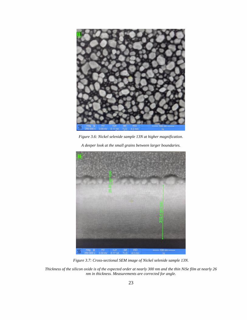
Figure 3.6: Nickel selenide sample 13N at higher magnification. .................................... 23
Figure 3.7: Cross-sectional SEM image of Nickel selenide sample 13N. ........................ 23
Figure 3.8: 2Θ grazing incidence plot of CoSe Sample 19............................................... 25
Figure 3.9: 2Θ grazing incidence plot of CoSe sample 16 ............................................... 25
Figure 3.10: XRD of CoSe sample 19 taken at a slightly different orientation in the
sample chamber. ............................................................................................................... 26
Figure 3.11: XRD 2Θ grazing incidence plot of NiSe sample 13N.................................. 27
Figure 3.12: Graphs of CoSe and NiSe overlaid atop each other. .................................... 28
Figure 3.13: XRD diffraction data of a CoSe/NiSe Heterostructure. .............................. 28
Figure 3.14: Nickel Selenide sample 13N high resolution XPS spectra........................... 30
Figure 3.15: Nickel selenide sample 13N Se 3D5/2 and Se 3D3/2. ................................. 31
Figure 3.16: Main Raman excitation modes of TMDs. .................................................... 32
Figure 3.17:Raman spectra CoSe sample 2. ..................................................................... 33
Figure 3.18: : Raman spectra CoSe sample 19. ................................................................ 33
Figure 3.19: Raman spectra NiSe sample 13N. ................................................................ 34
Figure 4.1: Sub orbital graph. ........................................................................................... 38
Figure 4.2: Mock graphs of basic magnetic responses in M vs H graphs. ....................... 41
Figure 4.3: Temperature averaged VSM data of cobalt selenide sample 14. ................... 44
Figure 4.4 Raw data of Cobalt Selenide tested on an MPMS-3 at 1.8 K.......................... 46
Figure 4.5: CoSe sample 19 mag data taken at 1.8 K ....................................................... 47
Figure 4.6: NiSe sample 13N mag data taken at 1.8 K ..................................................... 47
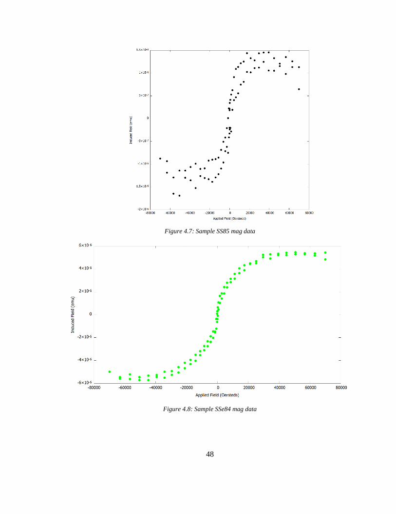
Figure 4.7: Sample SS85 mag data ................................................................................... 48
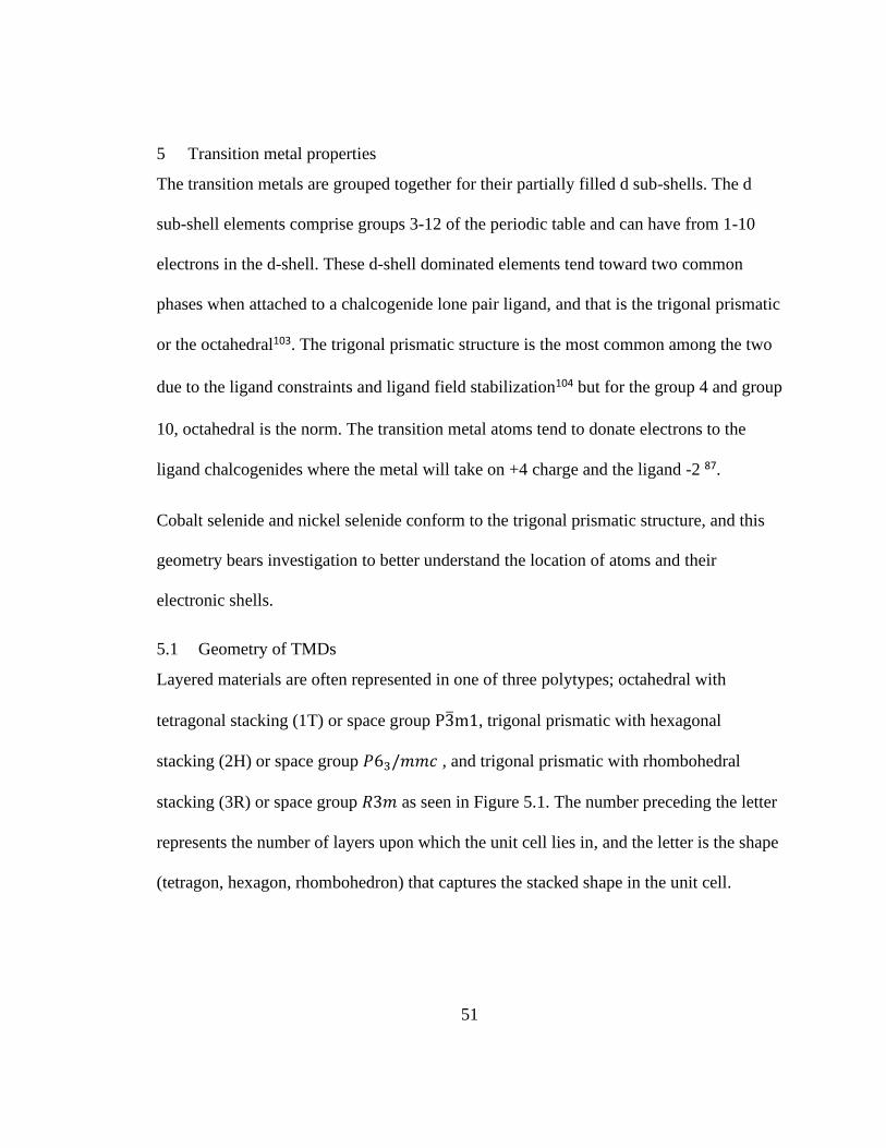
Figure 4.8: Sample SSe84 mag data ................................................................................. 48
Figure 5.1: Polyphases of hexagonal materials................................................................. 52
Figure 5.2: CoSe in hexagonal form 2H on the ab-plane (top-view)................................ 53
Figure 5.3: 2H cobalt selenide-side view of the bc-plane. ................................................ 53
ix
Figure 5.4 Atomic orbital cloud representation for the d-orbitals. ................................... 54
Figure 5.5 Energy diagram for the d-orbitals in cobalt selenide....................................... 55
Figure 6.1: Single layer cobalt selenide with c = 5.23 Å unit cell structure. .................... 63
Figure 6.2:Single layer cobalt structure with large vacuum layer included. .................... 64
Figure 6.3: POSCAR file for singly layer CoSe. .............................................................. 64
Figure 6.4: Total energy vs length of vacuum in the unit cell. ......................................... 65
Figure 6.5 Structures garnered from DFT calculations. ................................................... 69
Figure 6.6: HIVE STM faux scanning tunneling microscope image................................ 70
Figure 6.7: HIVE STM image with overlay. .................................................................... 71
Figure 6.8 Cobalt selenide valence charge density map on ab plane. ............................... 72
Figure 6.9 Cobalt selenide spin up electron density for a few layer film. ........................ 72
Figure 6.10: Spin mapped Cobalt selenide at terminal end. ............................................. 73
Figure 6.11 Charge density map of few layer nickel selenide on ab plane. ..................... 73
Figure 6.12 Charge density map of few layer nickel selenide on ac plane. ...................... 74
Figure 6.13: Density of states graphs for cobalt selenide structures. ................................ 78
Figure 6.14: Density of states graphs for nickel selenide structures. ................................ 79

1
1 Introduction and Background
“What could we do with layered structures with just the right layers? What would the
properties of materials be if we could really arrange the atoms the way we want them?
They would be very interesting to investigate theoretically. I can't see exactly what would
happen, but I can hardly doubt that when we have some control of the arrangement of
things on a small scale we will get an enormously greater range of possible properties
that substances can have, and of different things that we can do.” ~ Feynman 1
Since Feynman’s 1969 talk of the “room at the bottom” there has been a search for the
methods and mechanisms that would allow us to manipulate and utilize thin film
structures at the atomic level. Twenty years later in 1989 when IBM 2 placed atoms to
form their iconic name on a surface with an AFM, and in 2004 when Geim and
Novoselov 3 experimentally showed the exfoliation of graphene, we came closer to the
realization of just what we really could achieve in terms of nano-scale manipulation.
Though the placement of gold atoms in a pattern was not necessarily a pivotal moment in
actualizing machines made at the atomic level, it showed the promise of more to come,
and much like the generation of graphene nanostructures did not prove to change the
computing world at the time, the door was opened to the reality of two dimensional
materials. Our group has taken a small step forward in this direction by characterizing a
2
class of layered materials, the two-dimensional transition metal chalcogenides, for their
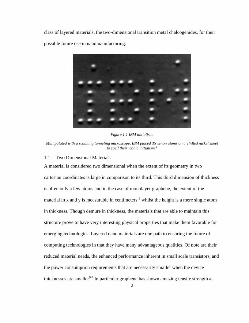
possible future use in nanomanufacturing.
Figure 1.1 IBM initialism.
Manipulated with a scanning tunneling microscope, IBM placed 35 xenon atoms on a chilled nickel sheet
to spell their iconic initialism.4
1.1 Two Dimensional Materials
A material is considered two dimensional when the extent of its geometry in two
cartesian coordinates is large in comparison to its third. This third dimension of thickness
is often only a few atoms and in the case of monolayer graphene, the extent of the
material in x and y is measurable in centimeters 5 whilst the height is a mere single atom
in thickness. Though demure in thickness, the materials that are able to maintain this
structure prove to have very interesting physical properties that make them favorable for
emerging technologies. Layered nano materials are one path to ensuring the future of
computing technologies in that they have many advantageous qualities. Of note are their
reduced material needs, the enhanced performance inherent in small scale transistors, and
the power consumption requirements that are necessarily smaller when the device
thicknesses are smaller6,7.In particular graphene has shown amazing tensile strength at
3
~300 times that of high quality steel8,9 and ballistic transport properties in conduction10–
12. From these interesting properties graphene found itself to have many commercial uses
such as nano-sized super capacitors, heatsinks, MEMs displays, and opto-electronics
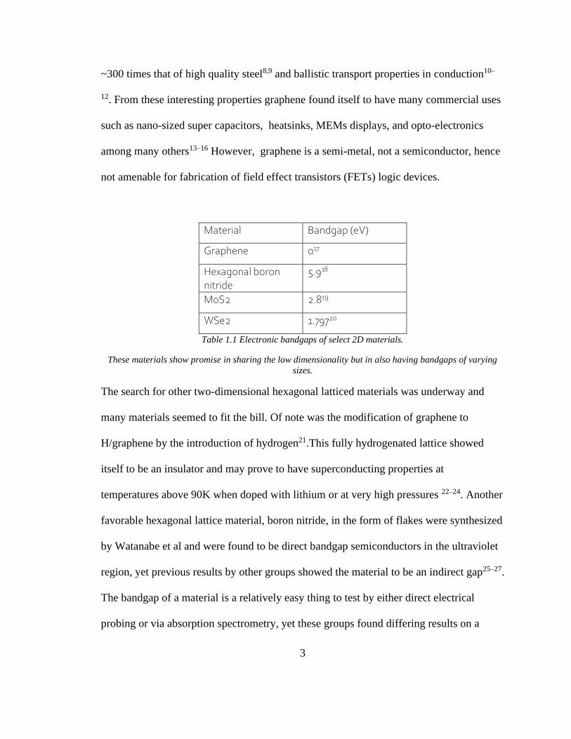
among many others13–16 However, graphene is a semi-metal, not a semiconductor, hence
not amenable for fabrication of field effect transistors (FETs) logic devices.
Material Bandgap (eV)
Graphene 017
Hexagonal boron nitride
5.918
MoS2 2.819
WSe2 1.79720
Table 1.1 Electronic bandgaps of select 2D materials.
These materials show promise in sharing the low dimensionality but in also having bandgaps of varying
sizes.
The search for other two-dimensional hexagonal latticed materials was underway and
many materials seemed to fit the bill. Of note was the modification of graphene to
H/graphene by the introduction of hydrogen21.This fully hydrogenated lattice showed
itself to be an insulator and may prove to have superconducting properties at
temperatures above 90K when doped with lithium or at very high pressures 22–24. Another
favorable hexagonal lattice material, boron nitride, in the form of flakes were synthesized
by Watanabe et al and were found to be direct bandgap semiconductors in the ultraviolet
region, yet previous results by other groups showed the material to be an indirect gap25–27.
The bandgap of a material is a relatively easy thing to test by either direct electrical
probing or via absorption spectrometry, yet these groups found differing results on a
4
morphologically same substance. It is in this area that the rub lies, many materials,
including the ones to be described herein, have qualities that are layer dependent
properties and appear to have morphological dependent properties as well.
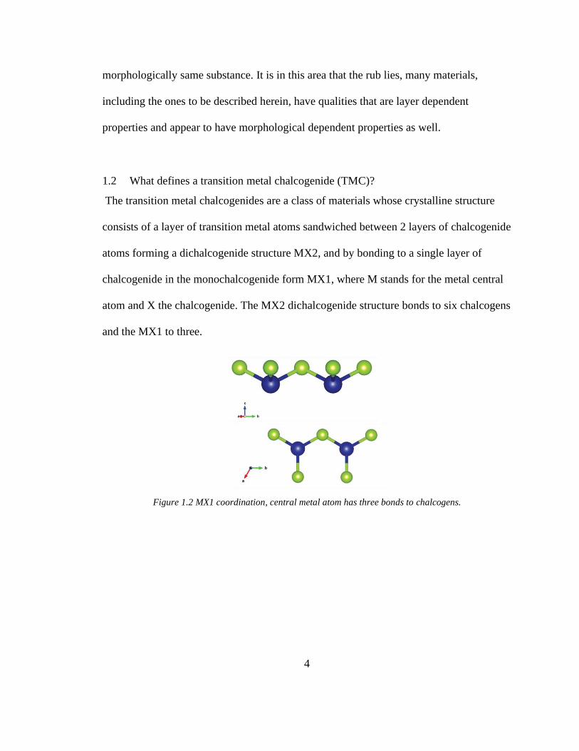
1.2 What defines a transition metal chalcogenide (TMC)?
The transition metal chalcogenides are a class of materials whose crystalline structure
consists of a layer of transition metal atoms sandwiched between 2 layers of chalcogenide
atoms forming a dichalcogenide structure MX2, and by bonding to a single layer of
chalcogenide in the monochalcogenide form MX1, where M stands for the metal central
atom and X the chalcogenide. The MX2 dichalcogenide structure bonds to six chalcogens
and the MX1 to three.
Figure 1.2 MX1 coordination, central metal atom has three bonds to chalcogens.

5
Figure 1.3 MX2 coordination where each metal atom has six distinct bonds.
These structures have many possibilities for coordination in that there are 38 transition
metals and 5 chalcogens on the periodic table.
Figure 1.4: Periodic table with transition metals in green and chalcogenides in blue
This makes for 190 distinct combinations of TMCs. The objective of this investigation is
specifically to examine how magnetism arises in TMCs. To that effect we chose as our
6
base materials the transition metals that show native magnetism, namely cobalt and
nickel. For our chalcogenides of choice, we selected sulfur and selenium. Magnetism
arises in materials primarily due to having unpaired spin electrons in the valence
electronic shell. Cobalt and nickel have three and two unpaired electrons respectively
which helps gives rise to ferromagnetism in these materials. Reports of various magnetic
states have been described in publications for these specific materials that range from
diamagnetic to ferromagnetic. In some cases different groups have given differing results
on the same make up of materials that may be due to the layering differences in the
samples tested28–36.
Magnetism and what gives rise to it is an interesting topic of study. The general
consensus for the mechanism for magnetism is that the unpaired spin states allow for
magnetic alignment, and the number and proximity of these unpaired spins determine the
domain structure that can lead to many flavors of magnetism. We can examine this in our
samples directly through the use of a SQuID magnetometer. These results can be
explained theoretically using ab-initio modeling through DFT. We have done both.
1.3 Historic endeavors into making TMD’s:
From as far back as 1923 with Portland, Oregon’s own Linus Pauling37 there has been
interest in the structures generated by the mixture of transition metals to that of the
chalcogenides and in their hexagonal layering structure. In 1927, NiS2 and CoS2 were
grown by Jong and Willem38, much like the materials described herein, garnered some
note as an interesting pyrite like material39, but they soon found themselves relegated to
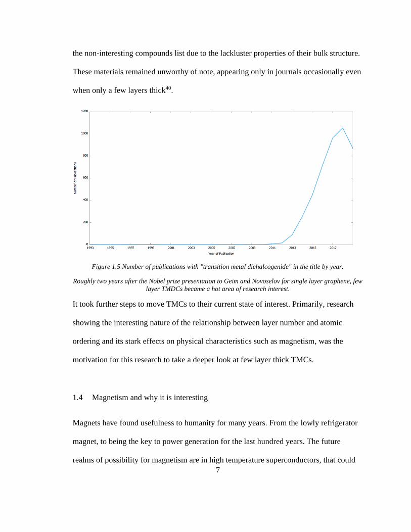
7
the non-interesting compounds list due to the lackluster properties of their bulk structure.
These materials remained unworthy of note, appearing only in journals occasionally even
when only a few layers thick40.
Figure 1.5 Number of publications with "transition metal dichalcogenide" in the title by year.
Roughly two years after the Nobel prize presentation to Geim and Novoselov for single layer graphene, few
layer TMDCs became a hot area of research interest.
It took further steps to move TMCs to their current state of interest. Primarily, research
showing the interesting nature of the relationship between layer number and atomic
ordering and its stark effects on physical characteristics such as magnetism, was the
motivation for this research to take a deeper look at few layer thick TMCs.
1.4 Magnetism and why it is interesting
Magnets have found usefulness to humanity for many years. From the lowly refrigerator
magnet, to being the key to power generation for the last hundred years. The future
realms of possibility for magnetism are in high temperature superconductors, that could

8
revolutionize the way we transmit power and in spin transistors, transistors that compute
not only via charge transfer but also based on the spin of the charge carrier41–43. Were we
to find materials that would break through in either of these fields, the benefit to the
scientific and technologic communities would be major. There are previous studies that
show TMDs may be a possible path to this34,44,45.
What is the mechanism for these magnetic orderings in materials? This question bothered
many scientists near the turn of the century and in part found explanations in the quantum
mechanics of the time, coupled with a serious look into coulombic interaction and the
crystallographic ordering of solids. Starting roughly with Weiss and his interpretation of
magnetic domains as the cause of ferromagnetism in materials46, it took Hund and his
rule for maximum multiplicity to bring the thinking of magnetism into the quantum
realm47. Under Hund, Weiss’s domains were described by the individual properties of the
electrons constituting those domains. Heisenberg and Dirac, in turn, developed the
exchange interaction of electrons48–53. This property of matter led to a real explanation of
the findings in magnetic materials using equation,
𝐸± = 𝐸(0) +
𝐶 ± 𝐽𝑒𝑥
1 + 𝑆2
1.1
where E+ is the spatially symmetric solution and E- the non, E(0) the initial energy, C the
Coulomb integral, S the overlap integral, and Jex the exchange integral. Including spin
into this equation yields
𝐽𝑎𝑏 =
𝐽𝑒𝑥 − 𝐶𝑆2
1 − 𝑆4
1.2
9
Jab is the exchange constant and in general, if the exchange constant is positive, the
material behaves ferromagnetically, and if negative, antiferromagnetically. The exchange
constant method proved to be problematic in metallic solids and thus other methods such
as those made by Stoner and Bloch that were delocalized in their electron placement
became the norm. This simple model has of course changed over time, but the salient
points remain the same. Magnetism is a quantum mechanical effect and the determination
of whether and how a material will react in a magnetic field is determined not only by its
constituents but also by the geographic positions of those elements.
The magnetic properties of TMCs have a history spanning decades. From scientists like
Adachi and Vandenburg studying the layered TMCs in their bulk39,54 to the
determinations of their van der Waal interactions and the frameworks of magnetism in
bulk by Richardson and Mandale55,56. Phase changes from tetragonal to hexagonal TMCs
by charge density waves and the first epitaxial growths from Motizuki and Saiki57,58.
And finally, the latest cycle of research in morphologies of TMCs of cobalt and nickel in
particular, done by Campos, Gruyters, Zhao, Moloto, Swesi, and Buchmaier et al59–64. It
is our goal to study two hexagonal thin film TMCs for their magnetic characteristics and
to find the root causes of that magnetism.
We have grown a few select thin films of transition metal chalcogenides and
characterized them using several techniques. Furthermore, we have performed
simulations on these materials from a first principles approach and checked to see that the
physical properties measured are well contained in the framework of our model. Chapter

10
two goes over the growth process of our TMD thin films. Chapter three describes the
non-magnetic physical characterization techniques and their results. Chapter four follows
into the magnetic results and how they were determined. Chapter five offers a review of
transition metal properties. Chapter six gives insight into density functional theory and
the process of first principle calculations in the Vienna ab initio simulation program.
Finally, chapter seven offers conclusion and insights to potential future work that can be
done to further the field of TMD thin film technologies.
11
2 Growth of Hexagonal Cobalt and Nickel Selenides
Material deposition techniques have grown over the years with many advances in
techniques such as physical vapor deposition (PVD), chemical solution deposition (CSD),
and chemical vapor deposition (CVD). The PVD methods are those that energize a target
material or source to the point that it liberates atoms or molecular species from its
surface. Common PVD methods are thermal evaporation, plasma sputtering, and
molecular beam epitaxy. The first two of those are mildly coarse in the approach and
though they can generate uniformity, they are not thought of as capable of the high
precision necessary for layered thin films of varied chemistry. The most notable property
lacking is the inability to maintain stoichiometry due to the varied deposition rates of
each element due to their unique vapor pressures and internal cohesive energies.
Molecular beam epitaxy on the other hand is done in a highly controlled environment of
ultra-high vacuum, with multiple crucibles for multiple elements and the potential for
atomic layering while keeping stoichiometry intact.
Chemical solution deposition (CSD) methods are those that rely upon chemistry within a
solvent that is either self-driven on the surface by reaction, through heating methods, or
driven by electric potentials65 . The CSD technique is admittedly one of the coarsest and
hardest to control. CSD produces thick films very quickly and certainly has its place in
surface material formation. Unfortunately, due to the variability of reaction rates,
temperature-rate dependences, and inhomogeneity of compound solutions, CSD remains
a more imprecise method for the generation of layered thin films.
12
The CVD techniques have proven themselves time and again to be the method of choice
for controlled thin film deposition66,67. The deposition is driven wholly by chemistry with
precursors in the gas phase. It has the advantage of being non-directional compared to
PVD and being more controllable in the parameter space than CSD. Gas phase reagents
are introduced to a substrate in a reaction chamber and either react or decompose on the
surface to create the deposition. The reagents, after reaction and layer formation, leave
behind an oft volatile compound that can be flushed out when the reaction is complete.
Atomic layer deposition (ALD), is a self-terminating CVD process, and is known for the
generation of pristine crystalline surfaces with long range ordering. Alternation of
precursor materials that chemically bond to the topmost surface of a substrate and are
then flooded out of the chamber by way of an inert gas to form layers in steps. This
methodology was chosen for the growth of films by our group.
2.1 Growth of two-dimensional CoSe and NiSe films
Atomic layer deposition (ALD) has been an accepted growth process since the mid
1970’s68. The process itself has evolved over the years from a very slow growth
technique where depositions were made in the course of days of manipulation of high
vacuum, to the current flow through models like the F-120 reactor that we use. The F-120
was built specifically for fast cycling and ease of operation68.
The process begins with a substrate to be coated. The substrate should be smooth and free
of any surface contamination. Silicon wafers with a CVD layer of oxide are great
candidates for substrates when properly cleaned. The silicon dioxide surface is

13
amorphous and offers a base that does not have a preset alignment for atoms on its
surface. Crystalline substrates do have this built in electrostatic alignment that can be
helpful for some growths. Substrates like sapphire (Al2O3) are particularly good for
growth of perovskite thin films but are best used when there is a near lattice match
between the film desired and the substrate, otherwise artifacts can occur during growth.
With a substrate cleaned and placed in the reaction chamber, the chamber can be pumped
down to a moderate (few mTorr) vacuum and heated. This serves the purpose of the
removal of water from the surface and cleaning of the headspace to remove any other
reactive species in the chamber. With the chamber emptied and the substrate at a
temperature sufficient for reaction, a flush of inert gas like nitrogen is used to clear any
water or other reactive species from the chamber. This will be the first of many flushes of
an inert gas.
Once a clean surface and headspace has been achieved, the first reactive material can be
added to the chamber. This can be done in many ways, but the main objective is to have
the vapor pressure of the material reached so it can flow into the chamber often carried by
an inert gas like dry nitrogen. The reactive species will bind itself to the substrate and due
to the chemisorption of the precursor. With appropriate choice of precursors, the
precursor molecules will not form clusters or multi-layers as the binding between the
precursor and the substrate surface is stronger. When all active sites on the surface are
taken up by the single molecule thick layer of material, another flush of inert gas will set
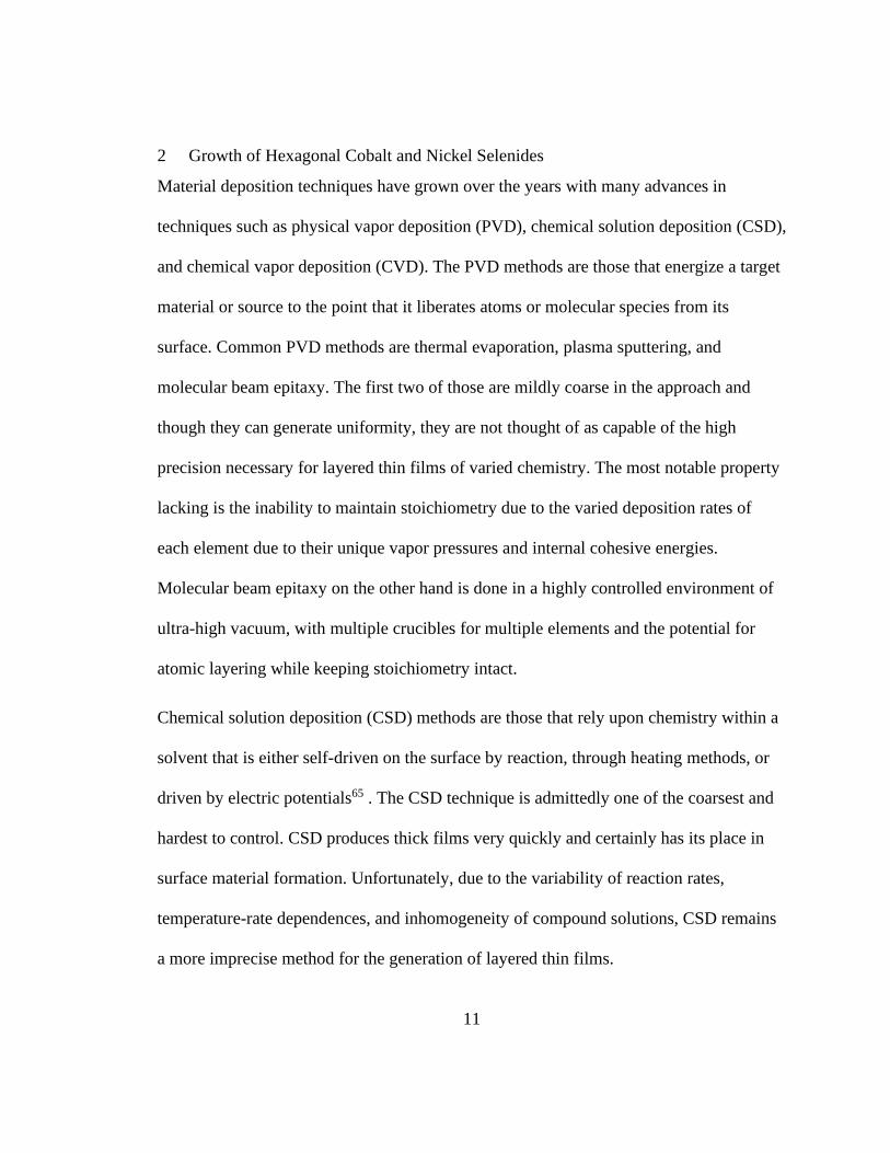
the chamber for the next species to be introduced as seen in Figure 2.1 a) and b).
14
This process continues with a new reactive material being introduced and subsequently
purged when surface reactions have concluded as seen in Figure 2.1 c) and d). This
process repeats until the atomically layered film is deposited to the desired thickness and
the chamber is lastly purged, cooled, and opened for sample retrieval.
Figure 2.1: Atomic layer deposition process.
a) A metal bound to a precursor is allowed into the growth chamber to react with the smooth silicon
dioxide surface b) After all available surface sites are filled, the chamber is purged with dry nitrogen to
remove excess metal + precursors c) Chalcogens bound to hydrogen as a precursor are introduced to the
chamber to react with the metallized surface d) Excess chalcogenides and precursors are removed from the
chamber with dry nitrogen. This process is repeated until the desired TMD thin film has the desired
number of layers.
NiSe and CoSe films were grown in a Microchemistry F-120 ALD reactor that can
handle two 50 mm x 50 mm substrates per run. The exhaust of the system included a
15
burn-box to decompose and trap any unreacted gases. The substrates for these films
consisted of p-type Si wafers coated with a 320 nm thick film of thermal silicon oxide.
The precursors for NiSe growth were nickel (II) acetylacetonate and H2Se (8%, balance
N2). The Ni source temperature was set at 170 °C and the carrier gas was nitrogen. The
pulse sequence per cycle was as follows; Ni source pulse width of 1 s; N2 purge of 1.0 s;
H2Se pulse width of 1.2 s; followed by 1.0 s N2 purge. Uniform film growth occurred
over a temperature range of 340 °C to 410 °C. The films reported here were grown at 390
°C, where the growth rate was 0.5 nm per cycle. The sources for CoSe films were Co (II)
acetylacetonate and the same Se source as above. The source temperature of the Co was
set at 175 °C. The pulse sequence was like that of NiSe films. Uniform films were
produced over a temperature range of 350 °C to 440 °C and the growth rate was 0.26
nm/cycle. There are many reaction pathways for the deposition of metals using metal-
ligand, metal + precursor, film growth. The actual surface reaction here was not
determined but likely follows that of Ir (III) acetylacetonate by Silvennoinen and
Merkx69,70.
The samples were then scored and cleaved with a diamond scribe for characterization. In
general, the sample size was anywhere from ~4 mm2 to 1 cm2.
16
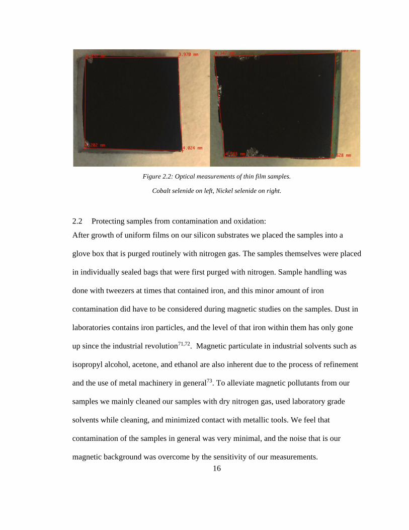
Figure 2.2: Optical measurements of thin film samples.
Cobalt selenide on left, Nickel selenide on right.
2.2 Protecting samples from contamination and oxidation:
After growth of uniform films on our silicon substrates we placed the samples into a
glove box that is purged routinely with nitrogen gas. The samples themselves were placed
in individually sealed bags that were first purged with nitrogen. Sample handling was
done with tweezers at times that contained iron, and this minor amount of iron
contamination did have to be considered during magnetic studies on the samples. Dust in
laboratories contains iron particles, and the level of that iron within them has only gone
up since the industrial revolution71,72. Magnetic particulate in industrial solvents such as
isopropyl alcohol, acetone, and ethanol are also inherent due to the process of refinement
and the use of metal machinery in general73. To alleviate magnetic pollutants from our
samples we mainly cleaned our samples with dry nitrogen gas, used laboratory grade
solvents while cleaning, and minimized contact with metallic tools. We feel that
contamination of the samples in general was very minimal, and the noise that is our
magnetic background was overcome by the sensitivity of our measurements.

17
Cobalt selenide and nickel selenide thin films were grown via atomic layer deposition.
The resulting films were of high optical quality in reflectance and appeared to have
uniform deposition over the SiO2 substrates. The samples were cleaved manually into
~2mm square sub samples for magnetic characterization and the remaining film surface
kept in an inert atmosphere for resampling should the need arise.
18
3 Non-magnetic Characterization
The thin film samples produced were tested via a multitude of physical characterization
techniques to ensure films of high purity and order. Surface characterizations such as
atomic force microscopy and scanning electron microscopy gave insight into the
uniformity of the samples surface and upon focused ion beam milling into lamella, a
rough estimate of the sample’s thickness. X-ray diffraction showed the high crystallinity
and phase of the samples, while x-ray photoelectric spectroscopy and Raman
spectroscopy gave further confirmation of the composition and phase of these films.
3.1 AFM:
Atomic force microscopy (AFM) offers an insight into the surface of a sample. The
technique is performed by carefully scanning a sharp tip, often in the range of 2-10
nanometers, over the sample’s surface. AFM work was completed using a Digital
Instruments D3000 NanoScope IIIa. The system was in tapping mode with a 10 nm
curvature tip.

19
Figure 3.1 AFM image of CoSe sample 19.
Surface clusters are of 50- a few hundred nm in size.
Figure 3.2 AFM image of Nickel Selenide sample 13.
No apparent clustering on the surface, high feedback levels in the PID loop introduce a wavy artifact to the
surface that was overall very flat.

20
3.2 SEM:
Scanning electron microscopy (SEM) is a surface metrology technique that employs
focused electrons accelerated to a samples surface inducing a secondary electron
emission (SEE) or backscatter emission (BSE) of electrons to be detected. The beam of
collimated electrons is then scanned over the surface and the number of backscatter or
secondary emitted electrons counted for each “pixel” of the generated surface image.
Though a surface technique, the depth of electron interaction can be modulated via the
accelerating potential to include some sub-surface features.
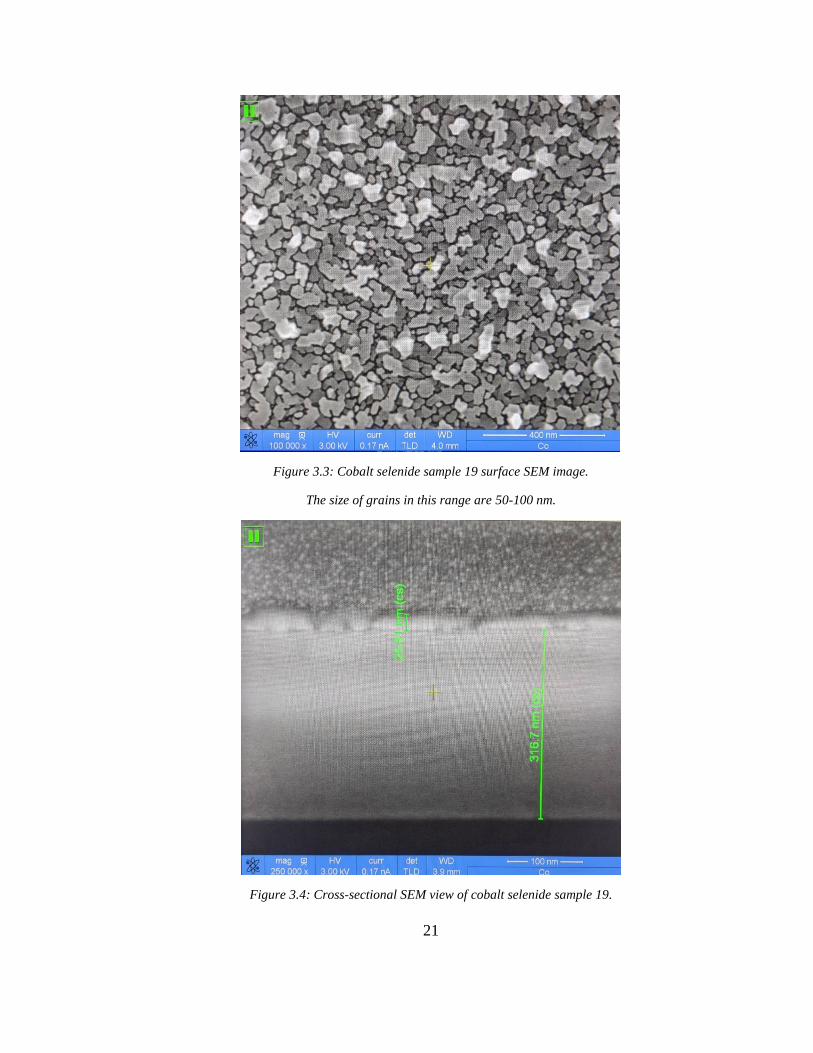
We have taken SEM images of our films both on the surface and on a freshly cleaved
cross-section. The top down images are uncoated. The cross-sections seen in Figure 3.4
and Figure 3.7 were coated with electron beam evaporated carbon and platinum for
protection prior to cleaving. The images were then recorded at 52° tilt with respect to the
electron beam.
Surface analysis showed growth of polycrystalline films, with grain size from tens of nm
to a few hundred in cobalt selenide and single digit nm to a few tens of nm for nickel
selenide as seen in Figure 3.3, Figure 3.5, and in higher relief in Figure 3.6. As these
films were grown on amorphous SiO2 surfaces, it is not surprising that the films were
polycrystalline.
21
Figure 3.3: Cobalt selenide sample 19 surface SEM image.
The size of grains in this range are 50-100 nm.
Figure 3.4: Cross-sectional SEM view of cobalt selenide sample 19.
22
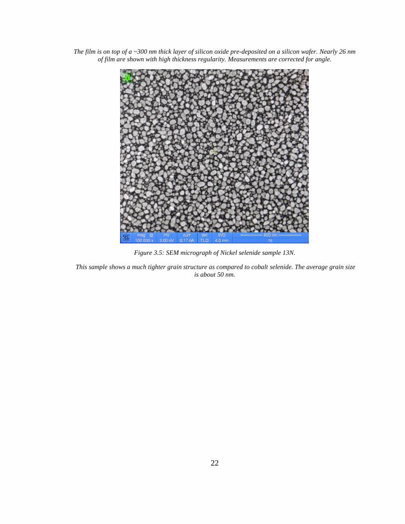
The film is on top of a ~300 nm thick layer of silicon oxide pre-deposited on a silicon wafer. Nearly 26 nm
of film are shown with high thickness regularity. Measurements are corrected for angle.
Figure 3.5: SEM micrograph of Nickel selenide sample 13N.
This sample shows a much tighter grain structure as compared to cobalt selenide. The average grain size
is about 50 nm.
23
Figure 3.6: Nickel selenide sample 13N at higher magnification.
A deeper look at the small grains between larger boundaries.
Figure 3.7: Cross-sectional SEM image of Nickel selenide sample 13N.
Thickness of the silicon oxide is of the expected order at nearly 300 nm and the thin NiSe film at nearly 26
nm in thickness. Measurements are corrected for angle.
24
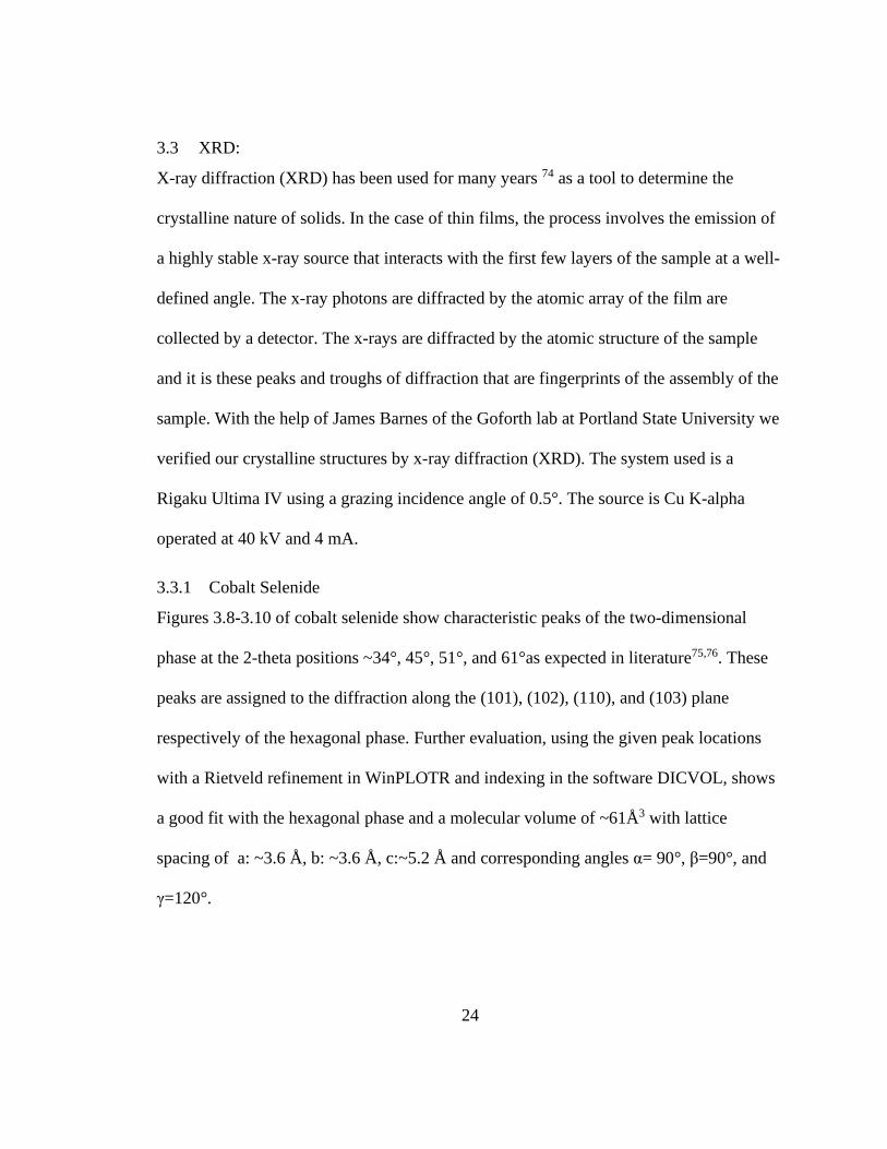
3.3 XRD:
X-ray diffraction (XRD) has been used for many years 74 as a tool to determine the
crystalline nature of solids. In the case of thin films, the process involves the emission of
a highly stable x-ray source that interacts with the first few layers of the sample at a well-
defined angle. The x-ray photons are diffracted by the atomic array of the film are
collected by a detector. The x-rays are diffracted by the atomic structure of the sample
and it is these peaks and troughs of diffraction that are fingerprints of the assembly of the
sample. With the help of James Barnes of the Goforth lab at Portland State University we
verified our crystalline structures by x-ray diffraction (XRD). The system used is a
Rigaku Ultima IV using a grazing incidence angle of 0.5°. The source is Cu K-alpha
operated at 40 kV and 4 mA.
3.3.1 Cobalt Selenide
Figures 3.8-3.10 of cobalt selenide show characteristic peaks of the two-dimensional
phase at the 2-theta positions ~34°, 45°, 51°, and 61°as expected in literature75,76. These
peaks are assigned to the diffraction along the (101), (102), (110), and (103) plane
respectively of the hexagonal phase. Further evaluation, using the given peak locations
with a Rietveld refinement in WinPLOTR and indexing in the software DICVOL, shows
a good fit with the hexagonal phase and a molecular volume of ~61Å3 with lattice
spacing of a: ~3.6 Å, b: ~3.6 Å, c:~5.2 Å and corresponding angles α= 90°, β=90°, and
γ=120°.

25
Figure 3.8: 2Θ grazing incidence plot of CoSe Sample 19
Figure 3.9: 2Θ grazing incidence plot of CoSe sample 16

26
Figure 3.10: XRD of CoSe sample 19 taken at a slightly different orientation in the sample chamber.
The small change in orientation is enough to significantly reduce the SiO2 background.
3.3.2 Nickel Selenide
Figure 3.11 of nickel selenide show XRD peaks at ~33°, 45°, 50°, 60°, and 62° in
agreement with chemical vapor deposition (CVD) grown films by Panneerselvam et al77.
These peaks again correspond to a hexagonal phase for the film with a volume of ~60Å3
with atomic spacing of a: ~3.6 Å, b: 3.6 Å, and c: 5.3 Å at 90°, 90°, and 120° respective
interatomic angles found via Rietveld analysis78.

27
Figure 3.11: XRD 2Θ grazing incidence plot of NiSe sample 13N
3.3.3 Heterostructure of Cobalt and Nickel Selenides
As more and more mono and few layer materials are produced, the ability to construct
heterostructure layers of them has become a topic of interest in modern materials science.
It has been shown that stacked monolayer materials form their own interesting super
lattices that may have beneficial properties for memory storage or quantum
computing79,80. We have manufactured cobalt selenide and nickel selenide films overlaid
upon each other. These films were built by substituting a cycle of one metal precursor for
another. By cycle: M1, X, M2, X, M1, X, M2, X, and so on, with M1 being the first metal
precursor, M2 the second, and X the chalcogenide precursor. The films grew on a cleaned
surface. The XRD data from the heterostructure seen in Figure 3.13 shows the peaks
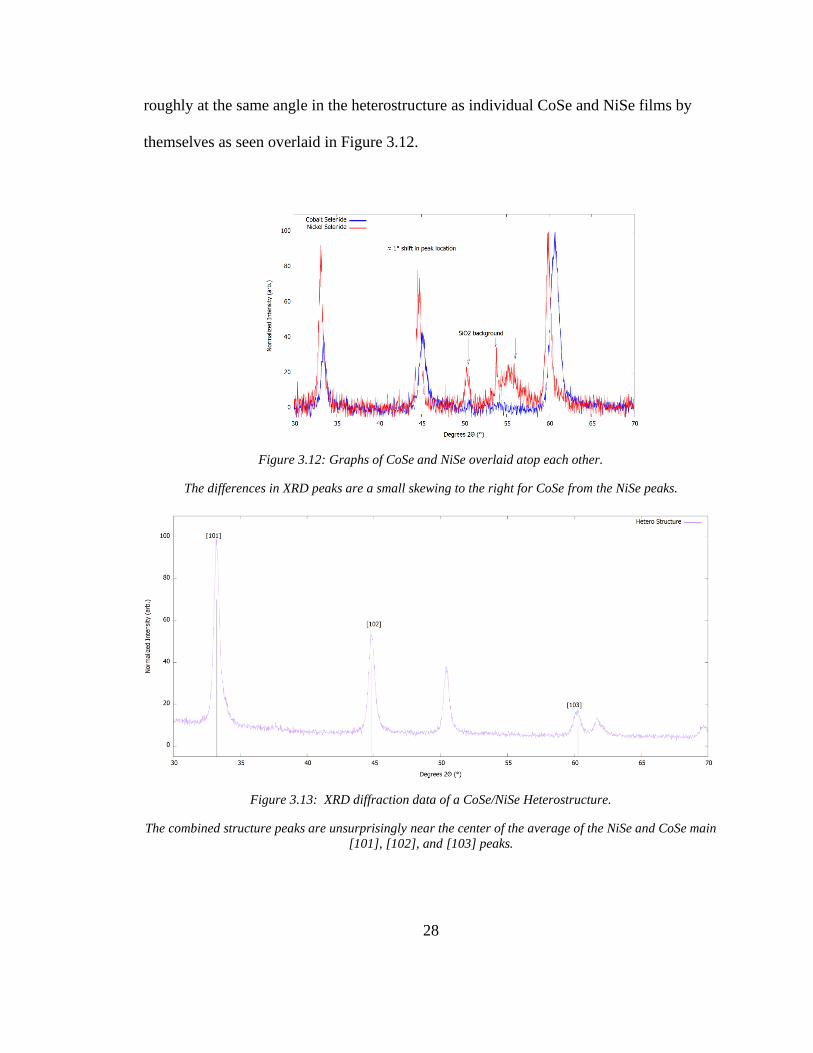
28
roughly at the same angle in the heterostructure as individual CoSe and NiSe films by
themselves as seen overlaid in Figure 3.12.
Figure 3.12: Graphs of CoSe and NiSe overlaid atop each other.
The differences in XRD peaks are a small skewing to the right for CoSe from the NiSe peaks.
Figure 3.13: XRD diffraction data of a CoSe/NiSe Heterostructure.
The combined structure peaks are unsurprisingly near the center of the average of the NiSe and CoSe main
[101], [102], and [103] peaks.
29
With these results at hand of XRD data that matches previous studies of cobalt and nickel
selenides, we are confident in the growth of hexagonal phase TMDs. The further growth
of a heterostructure of cobalt selenide and nickel selenide in alternating layers shows
XRD evidence of effective coupling between the CoSe and NiSe lattices that may lead to
interesting behaviors.
3.4 XPS:
X-ray photo emission spectroscopy (XPS) is a technique in which x-rays of a known
energy irradiate a surface and excite electrons from the surface. The electrons are then
captured, and their kinetic energies recorded. The resultant information offers an insight
into how tightly bonded the electrons are within the sample under test. Though one would
be tempted to believe that the valence electronic density of states could be directly
mapped through XPS, there are complications that prevent it from giving the full
electronic picture81–83. Nonetheless, XPS offers excellent characterization information as
it is a direct look into the electron interactions occurring in solids. The stoichiometry of
our samples and purity was determined via XPS performed on an Ulvac Phi 5000
VersaProbe II. Normal background subtraction and offset correction was performed
based on the adventitious carbon C-C peak as is standard practice.
3.4.1 Nickel Selenide
Figure 3.14 and Figure 3.15 show the Ni2p and Se3d electronic structures respectively.
The remaining peaks seen are satellites of the 3D levels and Ni 2P3/2 and it is likely that
the broadening seen is due to the polycrystalline nature of the film and an opening of the
30
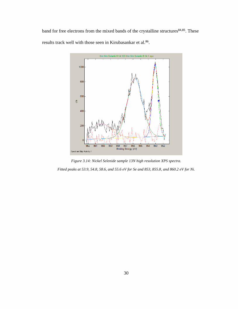
band for free electrons from the mixed bands of the crystalline structures84,85. These
results track well with those seen in Kirubasankar et al.86.
Figure 3.14: Nickel Selenide sample 13N high resolution XPS spectra.
Fitted peaks at 53.9, 54.8, 58.6, and 55.6 eV for Se and 853, 855.8, and 860.2 eV for Ni.
31
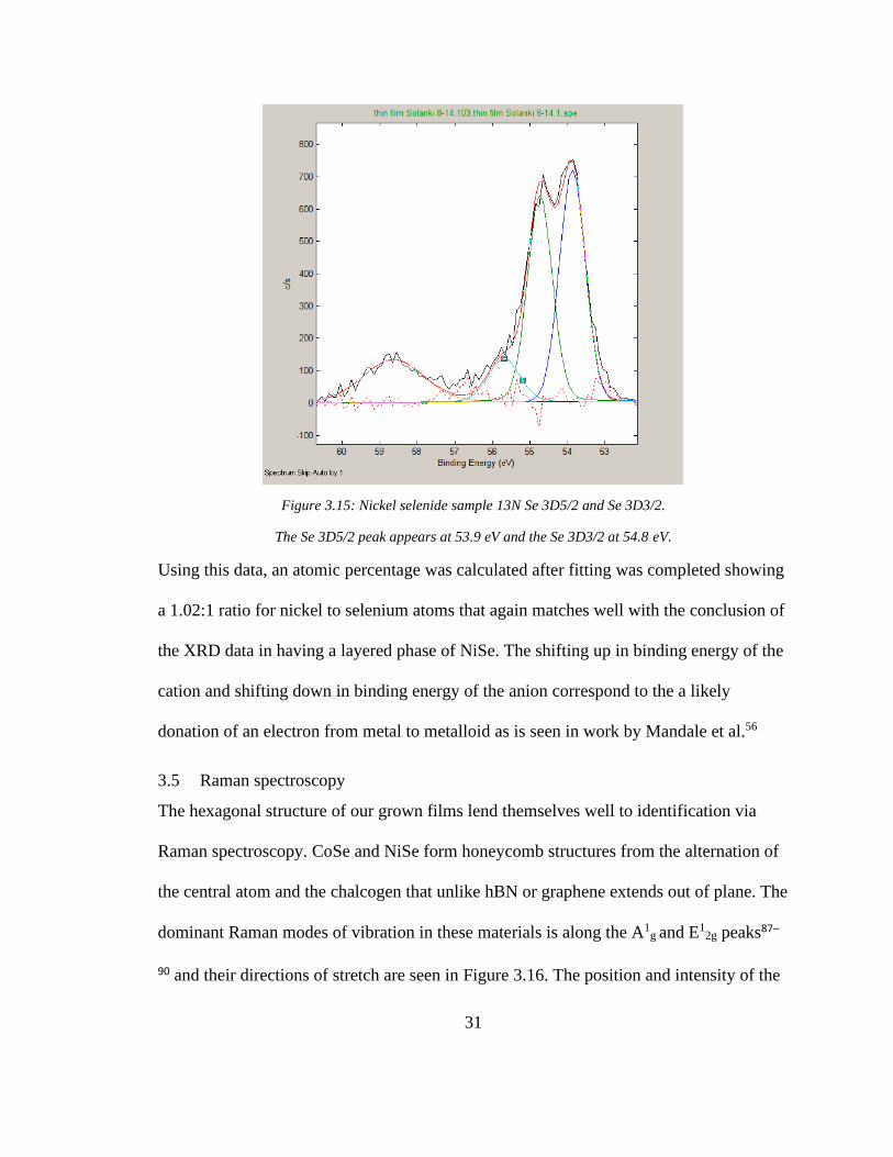
Figure 3.15: Nickel selenide sample 13N Se 3D5/2 and Se 3D3/2.
The Se 3D5/2 peak appears at 53.9 eV and the Se 3D3/2 at 54.8 eV.
Using this data, an atomic percentage was calculated after fitting was completed showing
a 1.02:1 ratio for nickel to selenium atoms that again matches well with the conclusion of
the XRD data in having a layered phase of NiSe. The shifting up in binding energy of the
cation and shifting down in binding energy of the anion correspond to the a likely
donation of an electron from metal to metalloid as is seen in work by Mandale et al.56
3.5 Raman spectroscopy
The hexagonal structure of our grown films lend themselves well to identification via
Raman spectroscopy. CoSe and NiSe form honeycomb structures from the alternation of
the central atom and the chalcogen that unlike hBN or graphene extends out of plane. The
dominant Raman modes of vibration in these materials is along the A1g and E1
2g peaks87–
90 and their directions of stretch are seen in Figure 3.16. The position and intensity of the
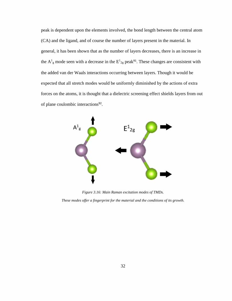
32
peak is dependent upon the elements involved, the bond length between the central atom
(CA) and the ligand, and of course the number of layers present in the material. In
general, it has been shown that as the number of layers decreases, there is an increase in
the A1g mode seen with a decrease in the E1
2g peak91. These changes are consistent with
the added van der Waals interactions occurring between layers. Though it would be
expected that all stretch modes would be uniformly diminished by the actions of extra
forces on the atoms, it is thought that a dielectric screening effect shields layers from out
of plane coulombic interactions92.
Figure 3.16: Main Raman excitation modes of TMDs.
These modes offer a fingerprint for the material and the conditions of its growth.
33
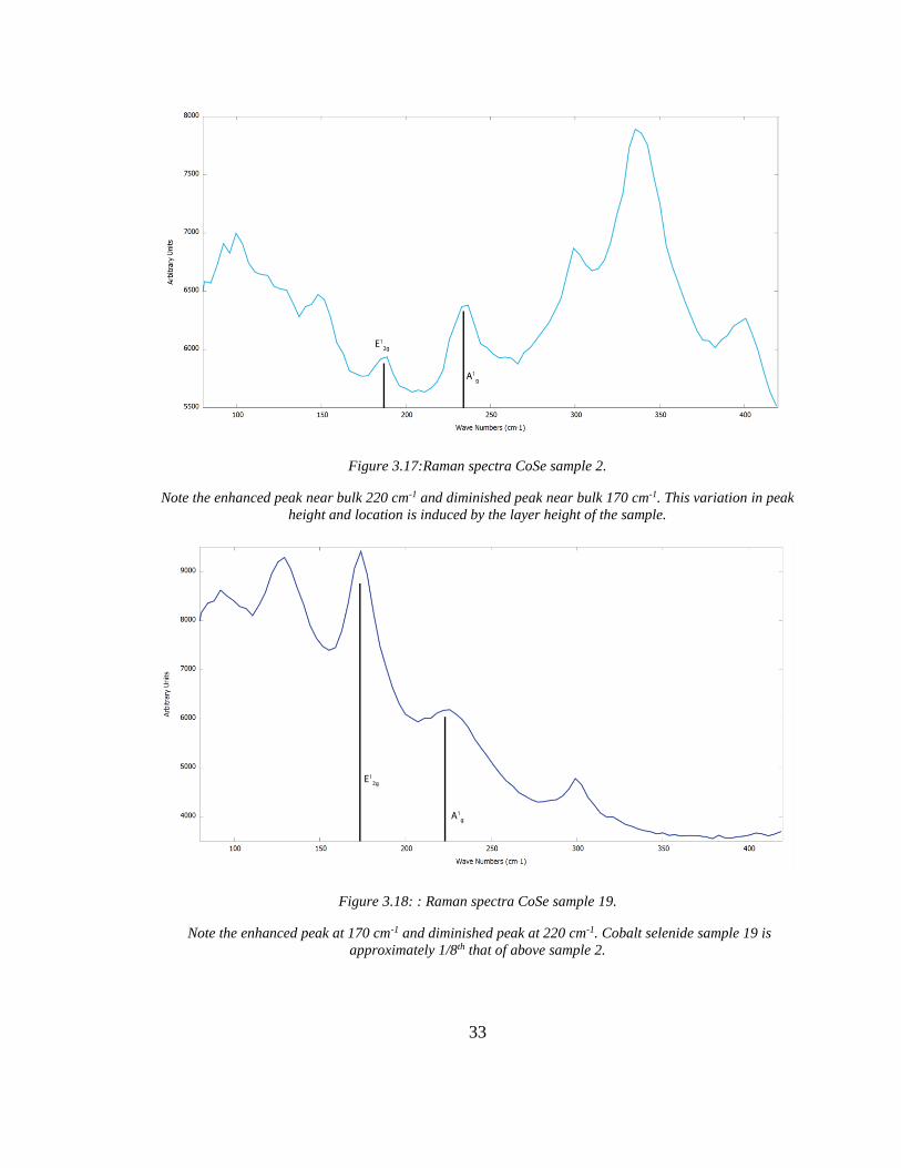
Figure 3.17:Raman spectra CoSe sample 2.
Note the enhanced peak near bulk 220 cm-1 and diminished peak near bulk 170 cm-1. This variation in peak
height and location is induced by the layer height of the sample.
Figure 3.18: : Raman spectra CoSe sample 19.
Note the enhanced peak at 170 cm-1 and diminished peak at 220 cm-1. Cobalt selenide sample 19 is
approximately 1/8th that of above sample 2.
34
Figure 3.19: Raman spectra NiSe sample 13N.
No major peak structures were found in this region.
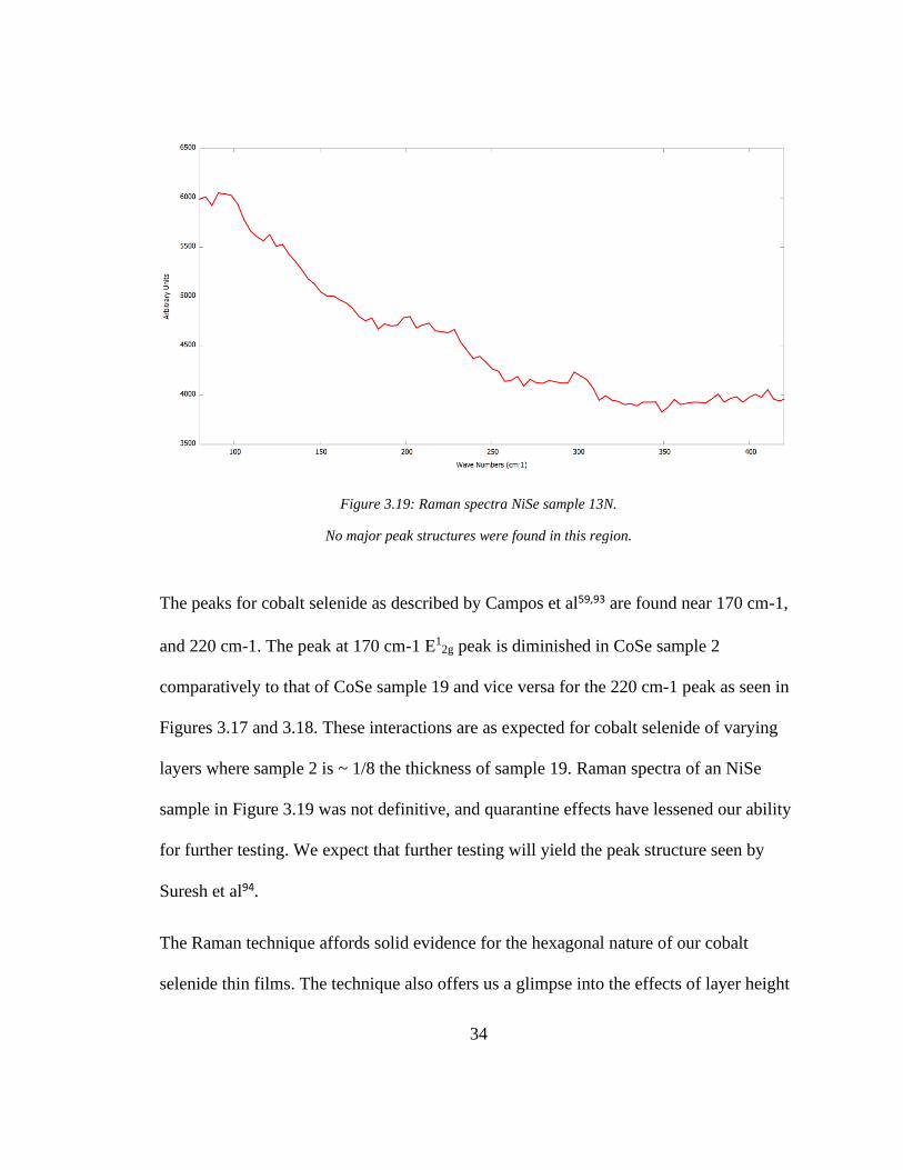
The peaks for cobalt selenide as described by Campos et al59,93 are found near 170 cm-1,
and 220 cm-1. The peak at 170 cm-1 E12g peak is diminished in CoSe sample 2
comparatively to that of CoSe sample 19 and vice versa for the 220 cm-1 peak as seen in
Figures 3.17 and 3.18. These interactions are as expected for cobalt selenide of varying
layers where sample 2 is ~ 1/8 the thickness of sample 19. Raman spectra of an NiSe
sample in Figure 3.19 was not definitive, and quarantine effects have lessened our ability
for further testing. We expect that further testing will yield the peak structure seen by
Suresh et al94.
The Raman technique affords solid evidence for the hexagonal nature of our cobalt
selenide thin films. The technique also offers us a glimpse into the effects of layer height

35
and interlayer forces that alter the inelastic scattering of photons by our films. It was
found that in cobalt selenide films the typical diminishment of the E12g peak with higher
layer stacking. These results should be tested on the nickel selenides, but an unforeseen
pandemic has damped the ability of testing. This work will be discussed in the further
research section. It is these layer dependent effects that may offer insight on the
differences in magnetism seen in TMC structures.
The non-magnetic physical characterizations performed have shown the crystalline phase
and geometry of our ALD grown samples. Our samples, both cobalt and nickel selenides,
appear to be hexagonally phased polycrystalline thin films of ~25 nm thickness. The
knowledge gained from these studies will inform the work done in chapter 6: DFT
studies, as will the magnetic characterization of chapter 4.
36
4 Magnetism in 2D films
A primary goal of our work is to patch a hole in the knowledge base of the magnetic
properties of TMDs. The magnetic properties of an element are determined based merely
on the number of unpaired electrons the element contains in a dance between what are
known as its spin and orbital angular momentum quantum numbers and their interaction
with each other, the spin orbit interaction . When a material moves toward a bonded
compound though, the lines become skewed as to the actual determinant of the magnetic
properties. In the simplest case we have no unpaired electrons leading to diamagnetism
and when there are some unpaired electrons which leads to paramagnetism. As we start to
add more elements together and move on to elements that are heavier things become
more complex.
As the elements themselves become heavier the spin orbit interaction of the element
becomes more pronounced. This leads to the peculiar effect in europium where, though
there are a number of unpaired spin states, the element acts diamagnetically due to the
interaction with its high angular orbital momentum. In the end the unpaired spins give
europium an overall paramagnetic response, the direct calculation of this response is
lessened by spin orbit interaction.
Magnetic properties of compounds can be determined using a hierarchy of methods that
have been devised by chemists and physicists alike over the last century. At the most
basic approach, magnetism can still be explained by the determination of paired or

37
unpaired spin states of electrons. This determination is balanced by the local fields
generated by the neighboring atoms.
Let us start with quantum numbers. There are four quantum numbers and they completely
describe the state of an electron in an atomic system. The first and most well-known is
the principal quantum number. It describes the energy level of an electron. In another
way it can be seen as a radial distance from the nucleus. The second is the azimuthal,
orbital, or angular quantum number. It describes the geometry of the probability cloud
that the electron can exist in. Chemically this is one of the most important numbers as it
describes the bonding capability of an electron. Thirdly is the magnetic quantum number.
This one is not a static as the others. The others describe the energy and the geometry
whereas this describes the available split states within an energy and geometry. The
fourth and final is the spin quantum number and it relates the ability of two electrons to
occupy an energy level.
38
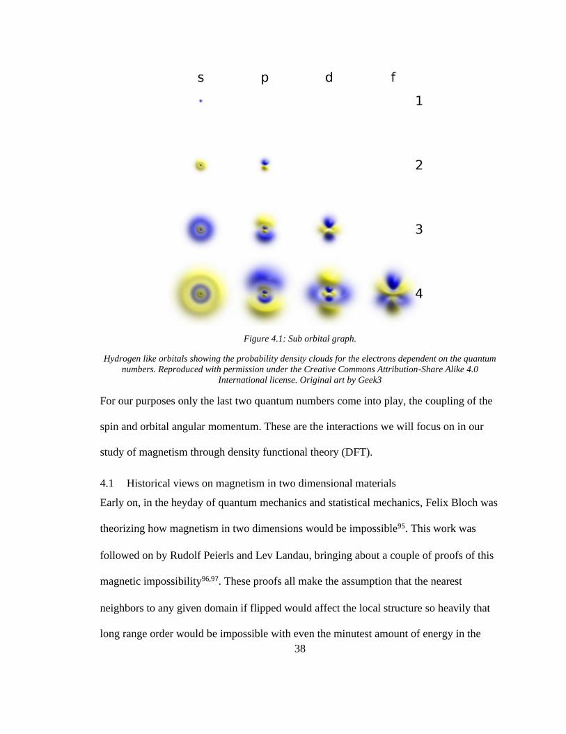
Figure 4.1: Sub orbital graph.
Hydrogen like orbitals showing the probability density clouds for the electrons dependent on the quantum
numbers. Reproduced with permission under the Creative Commons Attribution-Share Alike 4.0
International license. Original art by Geek3
For our purposes only the last two quantum numbers come into play, the coupling of the
spin and orbital angular momentum. These are the interactions we will focus on in our
study of magnetism through density functional theory (DFT).
4.1 Historical views on magnetism in two dimensional materials
Early on, in the heyday of quantum mechanics and statistical mechanics, Felix Bloch was
theorizing how magnetism in two dimensions would be impossible95. This work was
followed on by Rudolf Peierls and Lev Landau, bringing about a couple of proofs of this
magnetic impossibility96,97. These proofs all make the assumption that the nearest
neighbors to any given domain if flipped would affect the local structure so heavily that
long range order would be impossible with even the minutest amount of energy in the
39
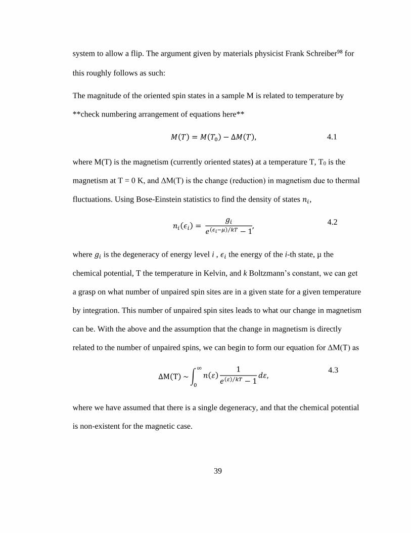
system to allow a flip. The argument given by materials physicist Frank Schreiber98 for
this roughly follows as such:
The magnitude of the oriented spin states in a sample M is related to temperature by
**check numbering arrangement of equations here**
𝑀(𝑇) = 𝑀(𝑇0) − ∆𝑀(𝑇), 4.1
where M(T) is the magnetism (currently oriented states) at a temperature T, T0 is the
magnetism at T = 0 K, and ΔM(T) is the change (reduction) in magnetism due to thermal
fluctuations. Using Bose-Einstein statistics to find the density of states 𝑛𝑖,
𝑛𝑖(𝜖𝑖) = 𝑔𝑖
𝑒(𝜖𝑖−𝜇) 𝑘𝑇⁄ − 1, 4.2
where 𝑔𝑖 is the degeneracy of energy level i , 𝜖𝑖 the energy of the i-th state, µ the
chemical potential, T the temperature in Kelvin, and k Boltzmann’s constant, we can get
a grasp on what number of unpaired spin sites are in a given state for a given temperature
by integration. This number of unpaired spin sites leads to what our change in magnetism
can be. With the above and the assumption that the change in magnetism is directly
related to the number of unpaired spins, we can begin to form our equation for ΔM(T) as
ΔM(T) ~ ∫ 𝑛(𝜀)
1
𝑒(𝜀) 𝑘𝑇⁄ − 1𝑑𝜀,
∞
0
4.3
where we have assumed that there is a single degeneracy, and that the chemical potential
is non-existent for the magnetic case.

40
In this equation when accounting for the dispersion relation between E and k leads to
𝑛(𝜀)~𝜀(𝑑−𝑛)
𝑛⁄ . 4.4
With d=2 for the two-dimensional space, and n=2 possible spin states leads us to 𝑛(𝜀) as
a constant.
Thus, the integral solution can take the form of
ΔM(T) ~ ∫
1
𝑥𝑑𝑥,
∞
0
4.5
which diverges toward zero. This means that for any T > 0 we see our reduction in
magnetism ΔM(T) as x trends toward infinity.
One way of obviating the solution to this proof of Mermin and Wagner is through
magnetic anisotropy. Magnetic anisotropic materials have a preferred direction for
magnetism. In 2D materials with high anisotropy, there is a chance of long-range
magnetism despite the above proof. Another aspect of anisotropy is that the so called
Ising ferromagnetism can occur in these solids, as shown in one and two layer thick iron
films by Back et al.99 A similar magnetic effect has been seen in TMDs such as MoSe2100,
CrI3 101, and NbSe2 44. These materials showed a spin orbit coupling (SOC) that coupled
spins perpendicular to the lattice faces that lined up with their adjacent spin sites, hence
displaying a magnetic effect44,100,101.
The origin of magnetism in materials is due to the configuration of electrons in that
material, but we see that spin and orbital momentum again act as the gateways to
magnetism in two dimensions.
41
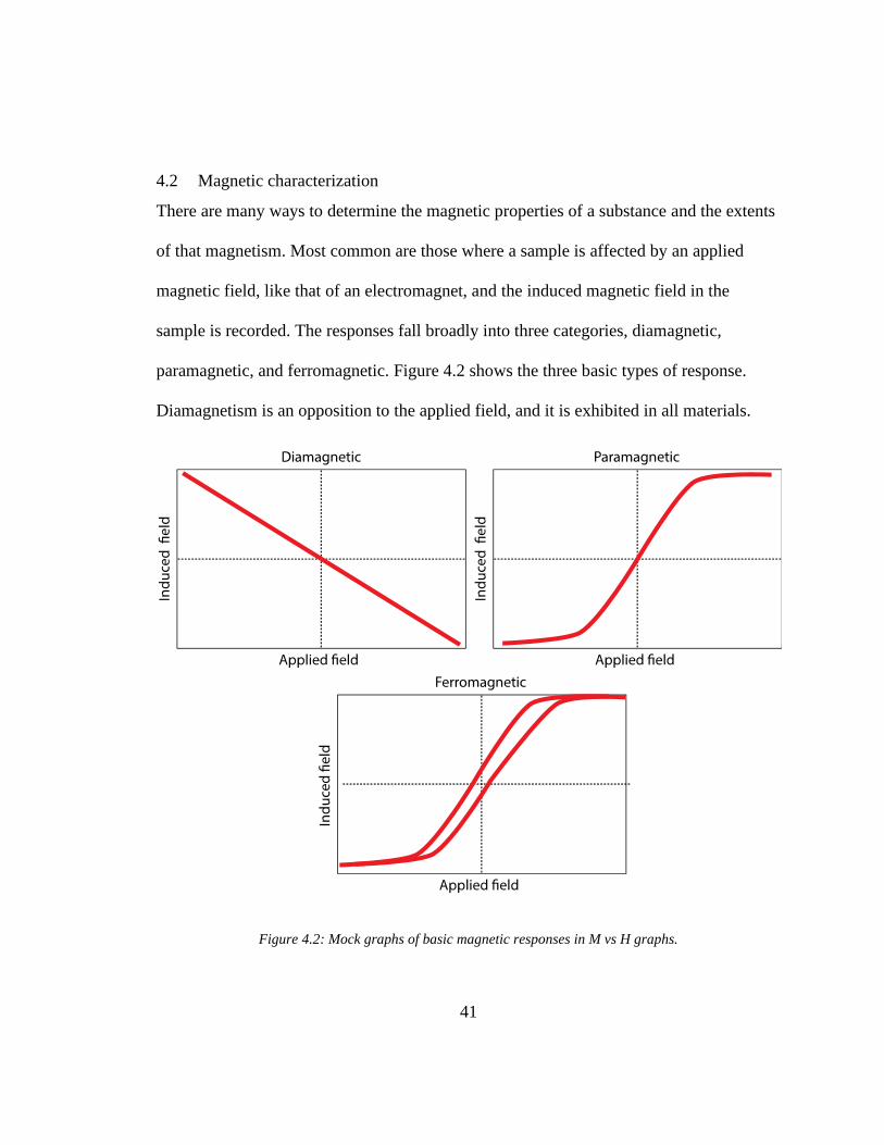
4.2 Magnetic characterization
There are many ways to determine the magnetic properties of a substance and the extents
of that magnetism. Most common are those where a sample is affected by an applied
magnetic field, like that of an electromagnet, and the induced magnetic field in the
sample is recorded. The responses fall broadly into three categories, diamagnetic,
paramagnetic, and ferromagnetic. Figure 4.2 shows the three basic types of response.
Diamagnetism is an opposition to the applied field, and it is exhibited in all materials.
Figure 4.2: Mock graphs of basic magnetic responses in M vs H graphs.
42
Though every material has some diamagnetic response, some materials have a
paramagnetic response that is strong enough to overcome it. This paramagnetic response
shows itself in the alignment to an applied magnetic field and thus when the applied field
is positive, so is the induced field. Finally, the ferromagnetic response is seen when once
a sample has aligned to an applied field, if that applied field is switched in polarity, there
is a resistance to that change in the induced field that is known as magnetic remanence.
There are other forms of magnetism, ferrimagnetism, anti-ferromagnetsim, super
paramagnetism to name a few, but the resulting interactions as seen in M vs H graphs are
just minor variations of the main three. We have investigated our samples via two
methods, vibrating sample magnetometry (VSM) and super conducting quantum
interference devices (SQuID).
4.2.1 VSM
Vibrating sample magnetometry is based upon Faraday’s law of induction wherein a
change in the flux of a magnetic field induces an electric field in the surrounding space.
This electric field can generate current in a conductor that can be detected by connected
circuitry. In this case a magnetic sample is placed within a strong magnetic field (many
Teslas) generated by an electromagnet and then vibrated at a known frequency. If the
sample is magnetizable, then under the influence of the applied field it will have its own
induced field. When vibrated, the current necessary to maintain a steady field in the
electromagnets can be monitored to give an idea of the magnetization of the sample.
Alternatively, a secondary conductive coil can be wrapped around the sample and
43
induced current within that coil can be detected as is the case with the measurement
system we used. The actual detection mechanism is a super conducting coil of wire that
collects the current caused by the changing magnetic field of the sample following
Maxwell Faraday law of induction:
𝛻 × 𝑬 = −𝜕𝑩
𝜕𝑡 ,
4.6
Our first samples were tested at the OSU applied magnetics laboratory with their
vibrating sample magnetomer (VSM) system by Quantum Design’s physical property
measurement system 14 (PPMS 14.) The operational limits of the PPMS are such that an
environment of -14 to 14 Tesla strength fields and 2 kelvin temperatures can be reached
with a sample under test. During a standard test, the sample would be purged many times
in a nitrogen atmosphere to remove any oxygen contamination. Oxygen in liquid form
has a paramagnetic field response. The sample would then be brought down to 2K while
under an external magnetic field strength of 8 Tesla. This field cooled situation allows for
the investigation of the temperature where the alignment of the domains in the material
may shift due to strong anisotropy in the material. This anisotropy would result in a dip
of the induced field as at a lower temperature it takes a stronger applied field to maintain
a high induced field by the equation
𝑇𝐵 =
𝐾𝑉
𝑘𝐵ln (𝜏𝑚
𝜏0)
4.7

44
where 𝑇𝐵 is the blocking temperature, K and V relate to the material’s magnetic isotropy
and volume respectively, 𝑘𝐵 the Boltzmann constant, 𝜏𝑚 as the measurement time and
𝜏0, the “attempt time”. This rearranging of the Neel-Arrhenius equation gives a
temperature that can be a fingerprint of superconducting activity.
Data was taken but did not offer an insight into the superconducting possibility of the
sample due to the granularity of the data. Figure 4.3 shows the quality of data taken on a
cobalt selenide sample.
Figure 4.3: Temperature averaged VSM data of cobalt selenide sample 14.
Field cooled cooling (FCC) data was taken at 8 Tesla field strength while the sample was cooled to 1.8K.
The noise level of the data precludes a real inspection for superconductivity.
There may be information hidden in the noise near the 75K temperature region, but this
could too easily be a liquid oxygen transition and not reflective of the sample at all. If
superconductivity does exist in the samples tested, it can be concluded it would be a
fragile state as no large peaks appear in this data. It was determined that a
superconducting quantum interference device (SQuID) measurement system would be
necessary to further investigate our samples.
-4.5E-08
-4E-08
-3.5E-08
-3E-08
-2.5E-08
-2E-08
-1.5E-08
0 50 100 150 200 250 300
Mag
ne
tic
Mo
me
nt
(Am
^2)
Termperature (K)CoSe-14 Temperatre Sweep Averaged

45
4.2.2 SQuID
A super-conducting quantum interference device (SQuID) can be used to infer the change
of the induced magnetic moment in a sample when placed under an applied magnetic
field. This task is done using a highly calibrated apparatus that both emits a uniform
magnetic field of varying strength and detects the existence of a changing magnetic field
by the detection of current in a coil. The sample is placed in a holder and then into a
specialized chamber that can be pumped down to a low vacuum. This chamber then has
the gasses evacuated from it and is backfilled with an inert gas (nitrogen.) This process is
done to remove as much water from the chamber and sample as is possible as even the
small magnetic dipole of water will be strongly seen in the device. In this case, as the
sample is held within a coil and the SQuID swings through large magnetic fields, the
sample aligns its induced magnetic field to the external SQuIDs magnetic field and
induces a current in the superconducting wire. This current then runs into a Josephson
junction that impedes conduction but allows for the counting of so-called magnetic flux
quantum, making some of the most precise measurements possible in magnetism.
This detection method again uses equation 4.6 in showing that B, the magnetic field,
when changing in time, generates a spatial change in E, the electric field. In this case, as
the sample is held within a coil and the SQuID swings through large magnetic fields, the
sample aligns its induced magnetic field to the external SQuIDs magnetic field and
induces a current in the superconducting wire. This current then runs into a Josephson
46
junction that impedes conduction but allows for the counting of the so-called magnetic
flux quantum, making some of the most precise measurements possible in magnetism.
4.2.2.1 SQuID Data
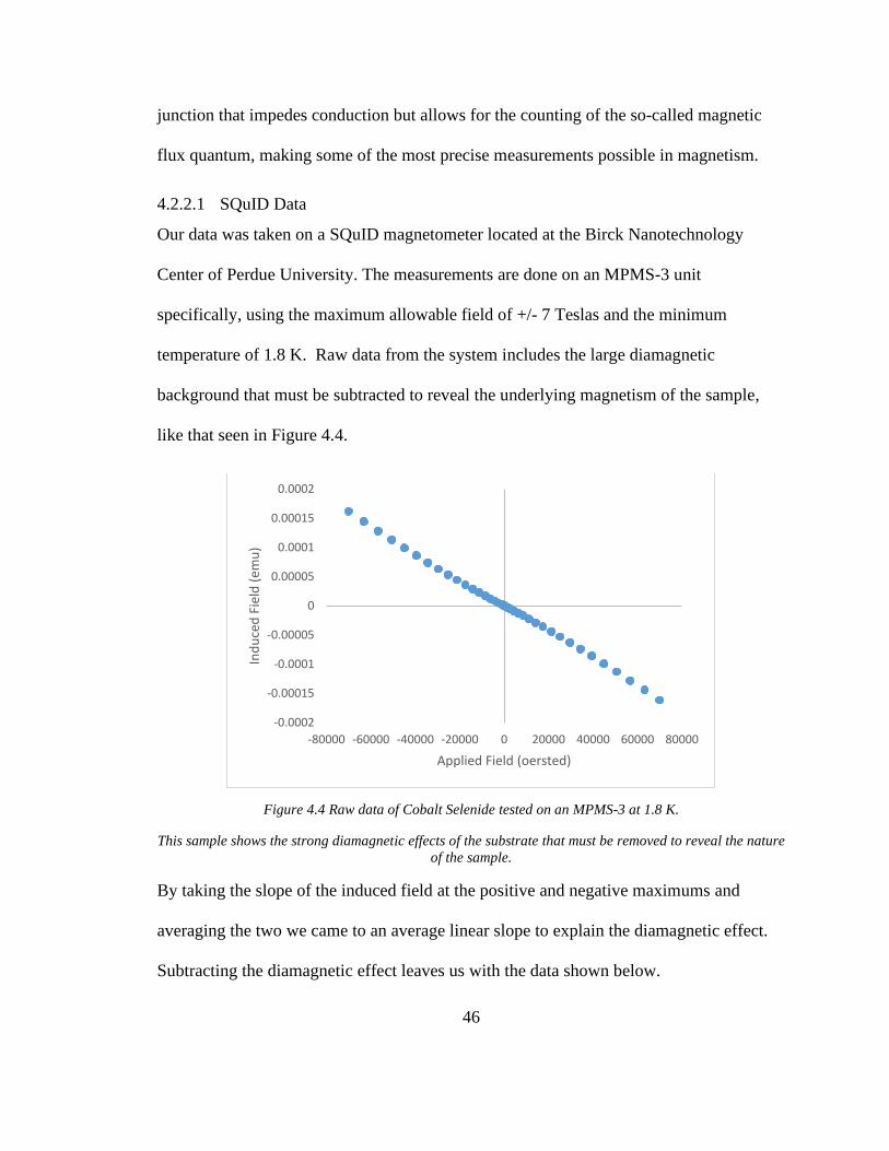
Our data was taken on a SQuID magnetometer located at the Birck Nanotechnology
Center of Perdue University. The measurements are done on an MPMS-3 unit
specifically, using the maximum allowable field of +/- 7 Teslas and the minimum
temperature of 1.8 K. Raw data from the system includes the large diamagnetic
background that must be subtracted to reveal the underlying magnetism of the sample,
like that seen in Figure 4.4.
Figure 4.4 Raw data of Cobalt Selenide tested on an MPMS-3 at 1.8 K.
This sample shows the strong diamagnetic effects of the substrate that must be removed to reveal the nature
of the sample.
By taking the slope of the induced field at the positive and negative maximums and
averaging the two we came to an average linear slope to explain the diamagnetic effect.
Subtracting the diamagnetic effect leaves us with the data shown below.
-0.0002
-0.00015
-0.0001
-0.00005
0
0.00005
0.0001
0.00015
0.0002
-80000 -60000 -40000 -20000 0 20000 40000 60000 80000
Ind
uce
d F
ield
(em
u)
Applied Field (oersted)

47
Figure 4.5: CoSe sample 19 mag data taken at 1.8 K
Figure 4.6: NiSe sample 13N mag data taken at 1.8 K
48
Figure 4.7: Sample SS85 mag data
Figure 4.8: Sample SSe84 mag data

49
Figures 4.4 to 4.7 show exemplary data from the MPMS-3. All the films that were tested
by our group showed paramagnetism to be the dominant phase and no magnetic
remanence revealed itself in our study.
The Van Vleck model of paramagnetism102 is best suited for samples that retain the
paramagnetic state at low temperatures and described as follows:
𝜇𝑒𝑓𝑓 = √3𝑘𝜒𝐴𝑇
𝑁𝛽2 ≈ 2.84√𝜒𝐴𝑇
4.7
can be described in terms of the effective magnetic moment µeff, where k = Boltzmann’s
constant, T = absolute temperature, N is Avogadro’s number, and χA is the susceptibility
per gram of the paramagnetic ion. Table 4.1 shows the experimental values in Bohr
magnetic moment for the CoSe and NiSe samples.
Sample Name Experimental magnetic
moment (µB)
Cobalt Selenide 19 0.3839
Nickel Selenide 13N 0.2815 Table 4.1: Magnetic moments of samples as calculated from the Van Vleck model of paramagnetism.
These values are lower than expected possibly due to some blocking by the ligand structure. A spin only
calculation would be ~4 and ~2 for cobalt and nickel, respectively.
Magnetic characterization was completed on many samples of cobalt and nickel
selenides. The samples were tested under VSM but were not found to have a large
response indicative of a strong superconductive state. Squid magnetometry was
performed showing paramagnetism in all of our samples that can be described by Van
Vleck paramagnetism. The magnetic moment in Bohr magnetons was 0.3839 and 0.2815,

50
for cobalt selenide and nickel selenide, respectively. These values show that there is a
high likelihood of ligand shielding of magnetism in the samples.
51
5 Transition metal properties
The transition metals are grouped together for their partially filled d sub-shells. The d
sub-shell elements comprise groups 3-12 of the periodic table and can have from 1-10
electrons in the d-shell. These d-shell dominated elements tend toward two common
phases when attached to a chalcogenide lone pair ligand, and that is the trigonal prismatic
or the octahedral103. The trigonal prismatic structure is the most common among the two
due to the ligand constraints and ligand field stabilization104 but for the group 4 and group
10, octahedral is the norm. The transition metal atoms tend to donate electrons to the
ligand chalcogenides where the metal will take on +4 charge and the ligand -2 87.
Cobalt selenide and nickel selenide conform to the trigonal prismatic structure, and this
geometry bears investigation to better understand the location of atoms and their
electronic shells.
5.1 Geometry of TMDs
Layered materials are often represented in one of three polytypes; octahedral with
tetragonal stacking (1T) or space group P3̅m1, trigonal prismatic with hexagonal
stacking (2H) or space group 𝑃63/𝑚𝑚𝑐 , and trigonal prismatic with rhombohedral
stacking (3R) or space group 𝑅3𝑚 as seen in Figure 5.1. The number preceding the letter
represents the number of layers upon which the unit cell lies in, and the letter is the shape
(tetragon, hexagon, rhombohedron) that captures the stacked shape in the unit cell.
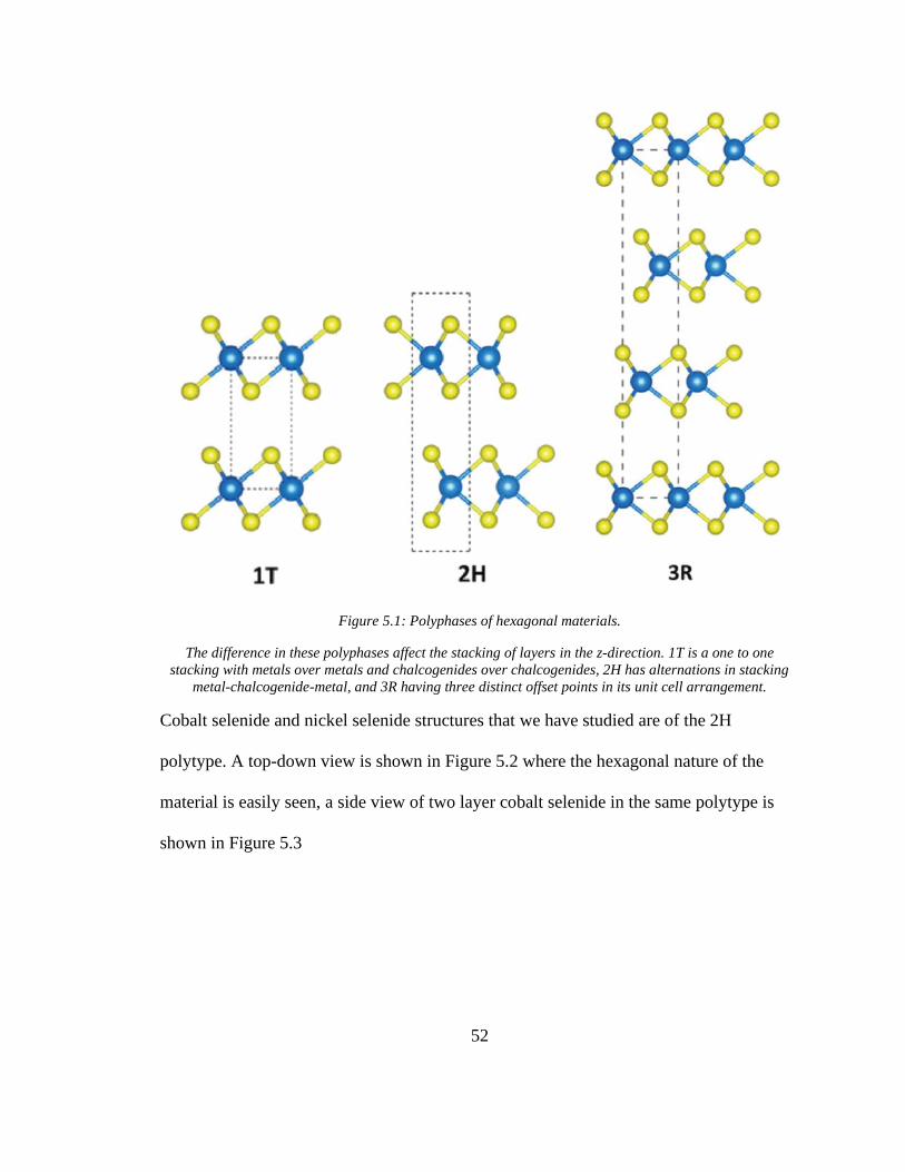
52
Figure 5.1: Polyphases of hexagonal materials.
The difference in these polyphases affect the stacking of layers in the z-direction. 1T is a one to one
stacking with metals over metals and chalcogenides over chalcogenides, 2H has alternations in stacking
metal-chalcogenide-metal, and 3R having three distinct offset points in its unit cell arrangement.
Cobalt selenide and nickel selenide structures that we have studied are of the 2H
polytype. A top-down view is shown in Figure 5.2 where the hexagonal nature of the
material is easily seen, a side view of two layer cobalt selenide in the same polytype is
shown in Figure 5.3

53
Figure 5.2: CoSe in hexagonal form 2H on the ab-plane (top-view).
Figure 5.3: 2H cobalt selenide-side view of the bc-plane.
Note the symmetry across the dotted line, this symmetry defines the 2H polytype.
5.2 Chemical theories of molecules
In order to understand the theoretical structure of transition metal complexes prior to
DFT calculations it is informative to determine the number of unpaired electrons. Simple
octet filling rules, such as the generation of Lewis structures, are too simple and neglect
54
to explain magnetic states of some complexes like O2105. Molecular orbital theory was
created to fill in that gap and works quite well for many structures but has the limitation
that it leaves degeneracy in the bonds of a particular orbit, i.e., 3d orbits have the same
energy in this model. This five-fold degeneracy is correct for simple metals, but since we
have coordination compounds, we will need ligand field theory to more correctly
describe the system. Ligand field theory is specific to transition metals and the
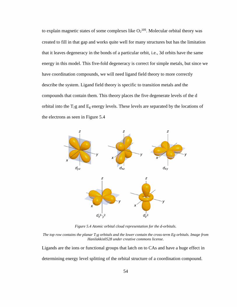
compounds that contain them. This theory places the five degenerate levels of the d
orbital into the T2g and Eg energy levels. These levels are separated by the locations of
the electrons as seen in Figure 5.4
Figure 5.4 Atomic orbital cloud representation for the d-orbitals.
The top row contains the planar T2g orbitals and the lower contain the cross-term Eg orbitals. Image from
Hanilakkis0528 under creative commons license.
Ligands are the ions or functional groups that latch on to CAs and have a huge effect in
determining energy level splitting of the orbital structure of a coordination compound.
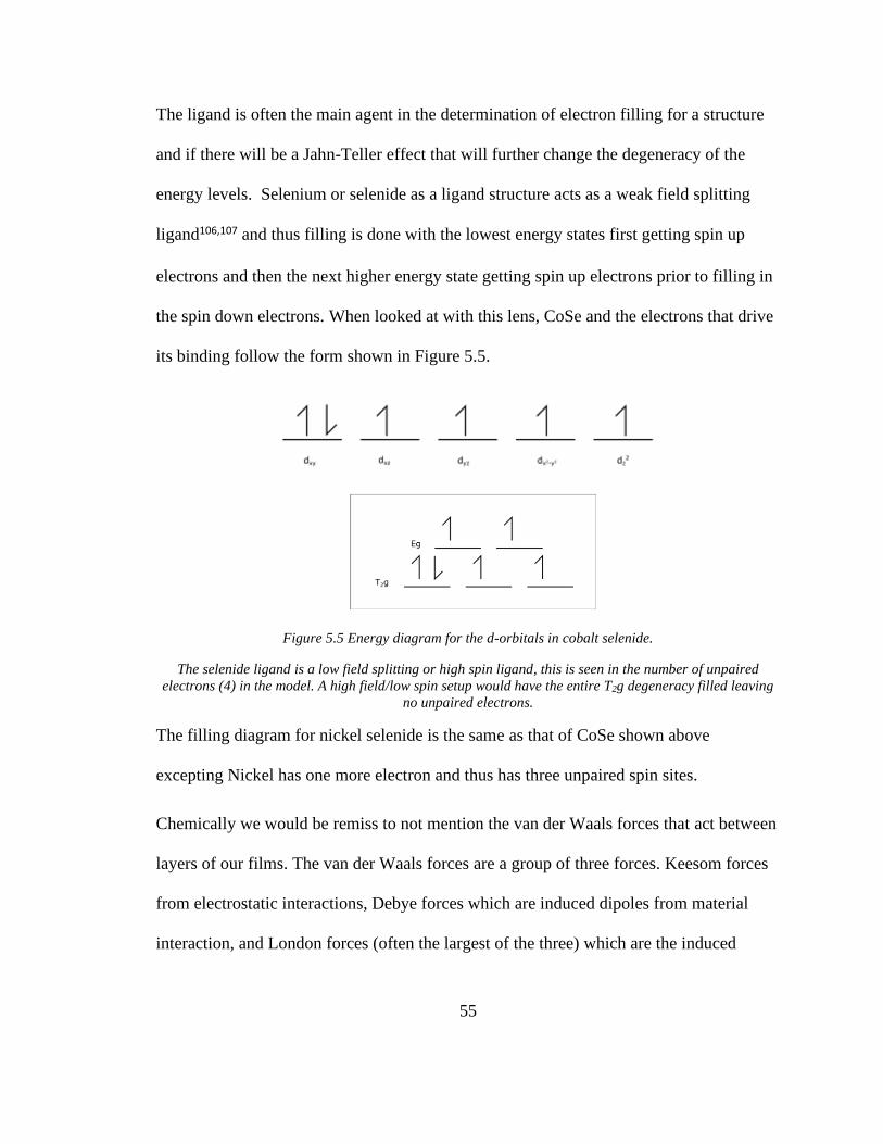
55
The ligand is often the main agent in the determination of electron filling for a structure
and if there will be a Jahn-Teller effect that will further change the degeneracy of the
energy levels. Selenium or selenide as a ligand structure acts as a weak field splitting
ligand106,107 and thus filling is done with the lowest energy states first getting spin up
electrons and then the next higher energy state getting spin up electrons prior to filling in
the spin down electrons. When looked at with this lens, CoSe and the electrons that drive
its binding follow the form shown in Figure 5.5.
Figure 5.5 Energy diagram for the d-orbitals in cobalt selenide.
The selenide ligand is a low field splitting or high spin ligand, this is seen in the number of unpaired
electrons (4) in the model. A high field/low spin setup would have the entire T2g degeneracy filled leaving
no unpaired electrons.
The filling diagram for nickel selenide is the same as that of CoSe shown above
excepting Nickel has one more electron and thus has three unpaired spin sites.
Chemically we would be remiss to not mention the van der Waals forces that act between
layers of our films. The van der Waals forces are a group of three forces. Keesom forces
from electrostatic interactions, Debye forces which are induced dipoles from material
interaction, and London forces (often the largest of the three) which are the induced
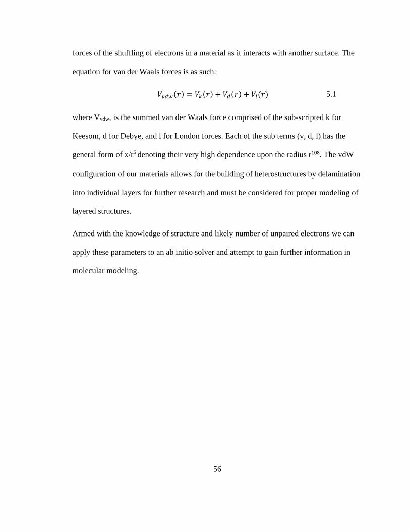
56
forces of the shuffling of electrons in a material as it interacts with another surface. The
equation for van der Waals forces is as such:
𝑉𝑣𝑑𝑤(𝑟) = 𝑉𝑘(𝑟) + 𝑉𝑑(𝑟) + 𝑉𝑙(𝑟)
5.1
where Vvdw, is the summed van der Waals force comprised of the sub-scripted k for
Keesom, d for Debye, and l for London forces. Each of the sub terms (v, d, l) has the
general form of x/r6 denoting their very high dependence upon the radius r108. The vdW
configuration of our materials allows for the building of heterostructures by delamination
into individual layers for further research and must be considered for proper modeling of
layered structures.
Armed with the knowledge of structure and likely number of unpaired electrons we can
apply these parameters to an ab initio solver and attempt to gain further information in
molecular modeling.
57
6 DFT: Modeling the origin of paramagnetism in NiSe and CoSe
“If you want to study function, study structure.” ~Francis Crick109
Some complex properties of materials are emergent, that is they do not appear out of
reduction. The ferromagnetism of iron is one example; how ferromagnetic is one iron
atom? One atom cannot be ferromagnetic, as the single atom has no neighbors to
influence into its magnetic domain. Thus, to study magnetism and other emergent
properties we must consider the transition metal compounds which often lend themselves
to the group of materials known as “strongly correlated materials.” This group is
distinguished by the fact that the correct description of the material must consider the
effects of each electron. This is why complex modeling involving both the core and
valence electrons must be done to predict the properties of these solids. This is the very
same reason why interesting properties can arise in these compounds due to the complex
interplay between the free d and f orbital electrons and their coulombic interaction with
each other.
VASP (Vienna ab-initio simulation package) is an ab-initio molecular dynamics solver
for density functional theory (DFT). It shines in its ability to solve complex geometric
exchanges from the first principles physics of quantum mechanics, electromagnetic
interactions and classical mechanics.
Brief background and framework of DFT
58
After the general acceptance of the Schrodinger equation as a definitive model of atoms
and their constituent parts, a search for methods of approximation began. The key issue
was the insolubility of many electron wave functions with the maths available at the time.
The first major approximation developed was by Douglas Hartree in the famous Hartree
approximation or self-consistent field method. This system, after refinement by the use of
Slater determinants from Vladimir Fock’s addition to the theory, became known as the
Hartree-Fock method. The method makes use of three approximations110:
• neglect relativity and spin in calculations
• neglect exchange and all wavefunction overlap effects
• the whole atom wavefunction is broken into functions based on the geometry of
each electron’s placement in that geometry
Dirac later summed up the Hartree-Fock method and the key element of density
functional theory in a report of the Cambridge Philosophical Society in 193049,
“if the total electric density is known at one time, then it can be known for any other time
via the equations of motion.”
This leads us to having one density matrix function describing a system, in place of a
significantly messier setup with individual wave functions for each atom in a system.
This is a major simplification as is known to anyone who has solved systems of single
wave equations and imagining the terror that would be in the solving a single atom of
carbon.

59
This Hartree-Fock method has also been called the self-consistent field (SCF) method
and is an iterative approach in trying to find the energy of a stationary group of many
atoms. This is done by making a superposition of so-called Linear Combinations of
Atomic Orbitals (LCAO.) In the most primitive form, it is an addition of the single
electron wave functions of each atom and merely summing them up. Or, adding all
possible positions for electrons for one atom in a system and summing all of that with the
other atoms paying special attention to the overlap. These areas of overlap form the
molecular orbital.
Furthering this idea Felix Bloch introduced a theorem that melded these ideas of
superposition with the regularity of crystalline solids. The Bloch theorem states that the
energy states of electrons in a crystal can be reproduced by Bloch waves. These waves
are the superposition of the energy plane waves of the electrons and the periodic potential
provided by the crystal lattice. Shown by the equation
𝜓(𝑟) = 𝑒𝑖𝐾∙𝑟𝑢(𝑟) ,
6.1
where 𝜓(𝑟) is the Bloch wave with respect to the radius r, K is the wave vector and 𝑢(𝑟)
is a potential that is periodically repeating in ‘r’ enforced by the crystal structure. These
wave functions are interestingly non-unique and can be generated with different
combinations of K and U(r). From Bloch’s periodic functions of crystals, we can move to
the Wannier functions to find some descriptions for the bonding that occurs in these
crystalline systems. The Wannier functions, particularly used here are the maximally
localized functions (MLWFs), that provide a localization for energy in real space and
60
thus allow the decoding of bonding in materials and appropriate disentangling of band
structures along symmetry points in a lattice and furthermore the non-symmetric as well.
These previous generations of quantum physicists and chemists set the stage for modern
computational solvers of elaborate many atom substances, wherein the solving of gigantic
equations was reduced to solving much smaller parts and summing them properly. These
methods are the protocol and framework of density functional theory.
6.1 Practical use of VASP
The first step in DFT is often the optimization of geometries. In order to do this, we used
the VASP program suite and the associated projector augmented wave (PAW) pseudo-
potentials set. We have chosen the Perdew-Burke-Ernzenhof (PBE) set for the exchange
correlations (XCs) and the gradient corrections on exchange and correlation. PBE XCs
are known for notoriously low estimates of ground states, but exceptionally good
optimizations of geometry.
The following approach was used. When we reach an equilibrated geometry, we move on
to pseudo-potentials, XCs, and algorithms that specifically take into account local spin
density and model as many electrons per atom as possible. These modellings allowed us a
better look at the interactions of the electrons not just at the valence level, but deeper into
the core. For the geometric model we make assumptions as to the motions and
placements of atoms in three space where it is absolutely non-essential to model any but
the outermost electrons, but when we move to electron interaction and band filling,
higher precision is necessary. To this effect we have chosen PAW PBE pseudopotentials
with the addition of the p-semi core states treated as valence (pv extensions) and varied

61
the calculation environment accordingly to accommodate the additional core electron
modeling and non-collinear spin orbit interactions.
With the more detailed calculations performed on the energies and occupations of
electrons in the solid we were able to map out the band structure, density of states, and
also get a realistic value of the magnetic moment of our materials.
6.1.1 Geometry optimization
Optimization calculations were performed on the Portland State University cluster. These
were performed in the VASP standard solver with the standard PBE pseudopotentials for
cobalt, nickel, and selenium. The process begins with generating a concatenated file of all
potentials in use (POTCAR.) Next is the generation of a positional map of the geometry
for all atoms in the unit cell (POSCAR.) This is done by taking our XRD data and the
Rietveld refinement values for the geometry of the grown film. Using this as our initial
conditions, we set the baseline calculation space for optimization. This included setting
the accepted values of energy minimization for completion of the calculation, the method
of determining the energy trend, in our case a modified conjugate gradient approximation
(CGA.)
62
The step process is as follows:
• Read the positions from the POSCAR
• Calculate the energy and interatomic forces
• Approximate the total energy from this and add a correction term
• Calculate the energy and interatomic forces
• Make a correction term that is based upon the slope of the determined energy
• Repeat until the chosen differentiation in energy between steps is met or a chosen
number of steps is reached.
• If the above did not yield a result, take the latest result of optimization
(CONTCAR) and rename it POSCAR and attempt optimization again until we get
a result.
The result of geometric optimization is a file that contains the likeliest positions of atoms
in a crystallographic arrangement. This can be read into a program such as VESTA
(Visualization for Electronic and Structural Analysis.)
6.1.1.1 Considerations for layered materials
The above procedure is appropriate for all materials, but for layered materials such as
ours we took the extra step of generating a large layer of vacuum in the unit cell in order
to model a layer without its interaction to its neighboring layers. The VASP suite is a
projected augmented wave calculator and due to this, its calculation space extends the
wave functions in all possible directions. This means that even if we were to place a unit
cell with a seemingly single layer of material, the calculation would run over all space

63
regenerating the unit cell in x, y, and z, effectively making infinite planes stacked upon
each other infinitely high. The solution is to add so much space in the unit cell such that
layers stacked upon each other are so far apart as to not be ‘seen’, or to not have any
effective changes to the energy minimums or interactions. Figure 6.1 shows a single layer
geometry of cobalt selenide, if the unit cell was that found in its bulk state of a = 3.6 Å, b
= 3.6 Å, c = 5.2 Å, a calculation would yield all atoms of note in multiple layers and have
a substantially different result than that of a unit cell with high vacuum layering as seen
in Figure 6.2. Figure 6.2 shows a unit cell with a ~12Å gap of vacuum that even though
VASP calculates the entirety of the space, it will have no interaction between layers and
thus offers insight into the substance as a thin film of layered material.
Figure 6.1: Single layer cobalt selenide with c = 5.23 Å unit cell structure.
Layers are close enough to each other to freely interact. VASP calculations on this geometry would not
yield single layer results as the layers are close enough to electronically communicate.

64
Figure 6.2:Single layer cobalt structure with large vacuum layer included.
In this instance 10 angstroms separate cobalt atoms in the c-direction keep the calculation from allowing
layer interference.
Figure 6.3: POSCAR file for singly layer CoSe.
The cartesian unit cell in angstroms is on top and the fractional unitless cell is shown on the bottom. The
large z-value of 20.83 Å is due to the large vacuum spacing added for this single layer calculation.

65
In order to determine the necessary vacuum layer size to isolate a single layer one can
start at an arbitrary distance, say 20 angstroms as that seen in Figure 6.3, and iterate to
lower distances and monitor the total energy for changes or distortions in the unit cell.
Figure 6.4: Total energy vs length of vacuum in the unit cell.
Varying the length of the z-direction and plotting vs Total energy we can find the approximate distance
layers must be from each other to have little influence. In this case any distance over 10 Å will suffice.
This method was used to generate a plot like that seen in Figure 6.4 for our materials. In
all situations, NiSe and CoSe of varied layered structures, a vacuum spacing of 12 Å or
higher yielded non-interaction between subsequent unit cells. More spacing can always
be used, but the extra resources required for large unit cells is a price paid in computation
time.

66
6.1.2 Generating SPM data with HIVE STM
Hive STM is a program created by Danny Vanpoucke that can be used to plot surface
charge densities taken from DFT calculations111. Hive takes charge density data and plots
the assumed interaction a scanning tunneling microscope (STM) tip would encounter
near the surface of a material. In effect these false STM maps provide a visual take on
electron locality that can be checked against other localization methods. Generation of
the files necessary for this visualization required performing an energy minimization of
the sample by geometric optimization with high valency, followed by a self-consistent
field calculation with all atomic positions fixed. From the above two-step calculation
process band decomposed partial density values were generated in the PARCHG file of
VASP using the LPARD = .TRUE. function.
6.1.3 Spin calculations
VASP has three main “builds”, STD, GAM, and NCL. STD, or standard, performs all of
the standard calculations for simulation in the most efficient way possible. STD is the
basis for most users, but when it comes to the introduction of spin and orbital momentum
electron interactions, the NCL or non-collinear build allows for calculations that take
these properties into account. The NCL build is just as optimized but will often take
longer as the calculation parameter space is much larger.
Our spin-based calculations were done with the NCL build and LSORBIT function
command set to ‘.TRUE.’. The pseudopotential files used were of the highest available
valency to fully take in as many aspects of the electron interactions as possible. It is from
67
these calculations that we can predict our most accurate density of states, Bohr magnetic
moments, and charge localizations.
6.1.4 van der Waals force calculations
VASP can take van der Waals forces (vdW) into account and can offer some insight into
the strength of these forces as well. In our calculations we used the IVDW = 4 tag. This
tag allows for vdW forces to be considered in all aspects of calculations including
interatomic stress tensors, ionic, atomic, and lattice relaxations. These are done using the
methodology described by Becke and Johnson as the dDsC or density dispersion
correction112,113. This addition helps to ensure our layer separations are correct and the
interaction between layers stay sensible.
6.2 DFT Results
Many calculations were performed using the above methodologies. Fine tuning for
optimal precision and calculation time led to a plethora of results to be parsed. The main
insights from DFT analysis were in the placement of atoms in the lattice for the lowest
energy state, total charge distribution, valence charge density difference, magnetic
moment, and magnetic state of the systems. In most instances results were garnered for
CoSe and NiSe, in single layer, two-layer, five layer, and bulk species.
6.2.1 Final structures
The predicted crystallographic geometries given from DFT modeling are the result of
iterative relaxation of individual atoms in a lattice. The results were as expected for the
bulk material, being very near those published in materials databases114. The results for
CoSe in single layer, two-layer, and in five-layer displayed in Table 6.1 show the trend of
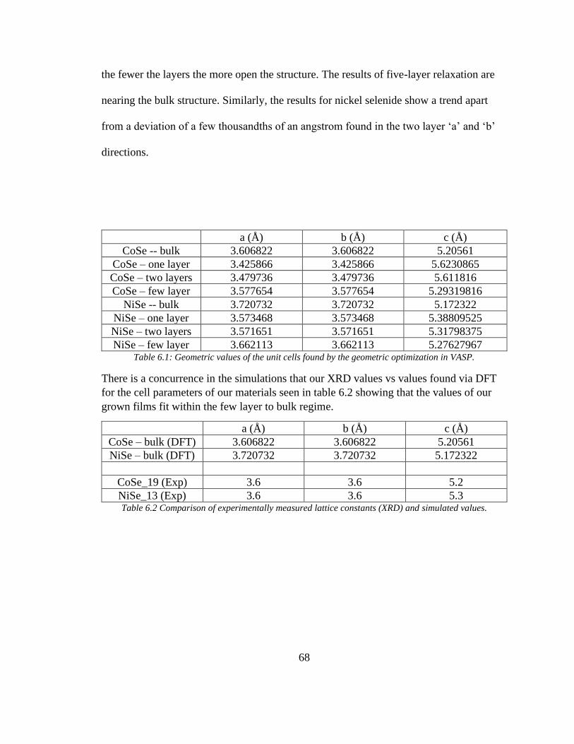
68
the fewer the layers the more open the structure. The results of five-layer relaxation are
nearing the bulk structure. Similarly, the results for nickel selenide show a trend apart
from a deviation of a few thousandths of an angstrom found in the two layer ‘a’ and ‘b’
directions.
a (Å) b (Å) c (Å)
CoSe -- bulk 3.606822 3.606822 5.20561
CoSe – one layer 3.425866 3.425866 5.6230865
CoSe – two layers 3.479736 3.479736 5.611816
CoSe – few layer 3.577654 3.577654 5.29319816
NiSe -- bulk 3.720732 3.720732 5.172322
NiSe – one layer 3.573468 3.573468 5.38809525
NiSe – two layers 3.571651 3.571651 5.31798375
NiSe – few layer 3.662113 3.662113 5.27627967 Table 6.1: Geometric values of the unit cells found by the geometric optimization in VASP.
There is a concurrence in the simulations that our XRD values vs values found via DFT
for the cell parameters of our materials seen in table 6.2 showing that the values of our
grown films fit within the few layer to bulk regime.
a (Å) b (Å) c (Å)
CoSe – bulk (DFT) 3.606822 3.606822 5.20561
NiSe – bulk (DFT) 3.720732 3.720732 5.172322
CoSe_19 (Exp) 3.6 3.6 5.2
NiSe_13 (Exp) 3.6 3.6 5.3 Table 6.2 Comparison of experimentally measured lattice constants (XRD) and simulated values.
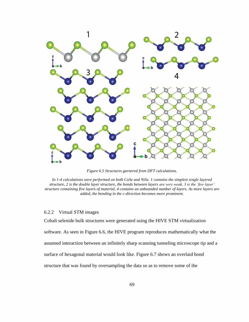
69
Figure 6.5 Structures garnered from DFT calculations.
In 1-4 calculations were performed on both CoSe and NiSe. 1 contains the simplest single layered
structure, 2 is the double layer structure, the bonds between layers are very weak, 3 is the ‘few layer’
structure containing five layers of material, 4 contains an unbounded number of layers. As more layers are
added, the bonding in the c-direction becomes more prominent.
6.2.2 Virtual STM images
Cobalt selenide bulk structures were generated using the HIVE STM virtualization
software. As seen in Figure 6.6, the HIVE program reproduces mathematically what the
assumed interaction between an infinitely sharp scanning tunneling microscope tip and a
surface of hexagonal material would look like. Figure 6.7 shows an overlaid bond
structure that was found by oversampling the data so as to remove some of the
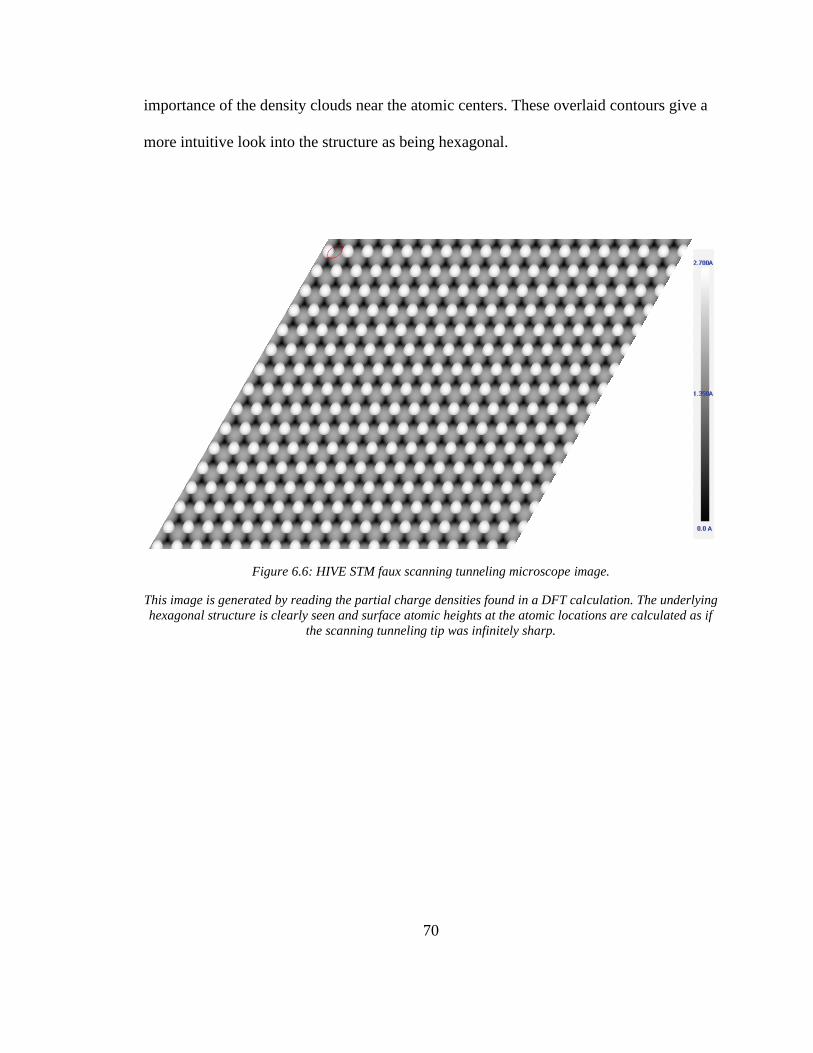
70
importance of the density clouds near the atomic centers. These overlaid contours give a
more intuitive look into the structure as being hexagonal.
Figure 6.6: HIVE STM faux scanning tunneling microscope image.
This image is generated by reading the partial charge densities found in a DFT calculation. The underlying
hexagonal structure is clearly seen and surface atomic heights at the atomic locations are calculated as if
the scanning tunneling tip was infinitely sharp.

71
Figure 6.7: HIVE STM image with overlay.
Overlay of bond structure showing hexagonal lattice in a cobalt selenide bulk structure.
Although the bond structures and edge states were not revealed in the STM display, the
hexagonal nature came through and show some potential for deriving information for
future studies. Splitting the spin states into positive and negative and generating a density
plot of their difference in VESTA was found to give more information on bonding and
spin localization.
6.2.3 Charge density maps in VESTA
Charge density maps were generated in VESTA via the methods proscribed by Pulkit
Garg et al115. The maps are the positions of electron density of the molecules with the sub
contributing portions of the individual atomic species removed. This technique leaves
behind the locations of electrons as bound by the system and presents a look at charge
density that is more granular than the bulk charge profiles given in false STM imaging.
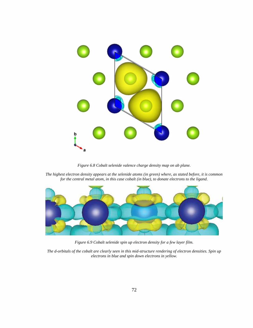
72
Figure 6.8 Cobalt selenide valence charge density map on ab plane.
The highest electron density appears at the selenide atoms (in green) where, as stated before, it is common
for the central metal atom, in this case cobalt (in blue), to donate electrons to the ligand.
Figure 6.9 Cobalt selenide spin up electron density for a few layer film.
The d-orbitals of the cobalt are clearly seen in this mid-structure rendering of electron densities. Spin up
electrons in blue and spin down electrons in yellow.

73
Figure 6.10: Spin mapped Cobalt selenide at terminal end.
Note the large bulbous cloud of electron density near the dark blue cobalt atoms that point away from the
green selenium bonding density. Spin up electrons in blue and spin down electrons in yellow.
Figure 6.11 Charge density map of few layer nickel selenide on ab plane.

74
Note as in the cobalt selenide structure the high propensity of density near the ligand selenium atoms.
Nickel atoms in silver and selenium in green.
Figure 6.12 Charge density map of few layer nickel selenide on ac plane.
The outermost nickel atoms do not show the same amount of electron density in the c-direction as does
cobalt of much the same geometry. Nickel atoms in silver and selenium in green, spin up electrons in blue
and spin down electrons in yellow.
Figures 6.8 and 6.11 show the valence charge density difference as calculated by
∆𝜌 = 𝜌𝑇𝑜𝑡 − 𝜌𝑚𝑒𝑡𝑎𝑙 − 𝜌𝑙𝑖𝑔𝑎𝑛𝑑 ,
6.2
where 𝜌𝑇𝑜𝑡 is the total charge density, 𝜌𝑚𝑒𝑡𝑎𝑙 is the density associated with the metal
atom calculated without the ligand present, and 𝜌𝑙𝑖𝑔𝑎𝑛𝑑 the density associated with the
ligand group without the metal atoms present. This valence charge difference shows us
the locations of valence electrons as calculated. It is unsurprising to see the high electron
density near the selenium atoms of both the NiSe and CoSe systems. Figure 6.9 shows
the d-orbital structure forming around the cobalt atoms found in the middle of the film
where the cobalt atoms are fully bonded. The interesting data shown in the difference
between Figure 6.10 and Figure 6.12 is that the cobalt structure has electrons pointing
away from the structure at the edge without selenium atoms. Those figures are the spin

75
separated densities as subtracted from the total density. These electrons can offer out of
plane magnetic effects as they are not locked into binding with the ligand group. The
same is not seen as dominantly in the NiSe map in Figure 6.12. The difference in edge
charge density and occupation near the edge may be the reason for a much more highly
pronounced magnetic moment showing in cobalt selenide than nickel selenide.
6.2.4 Average magnetic moment per metal atom
The Bohr magneton describes the average magnetic moment of a sample and is generally
measured in Bohr magnetons. It is the product of the spin magnetic moment, the orbital
magnetic moment, and the interplay between the two for each electron in a system. In the
case of the transition metals with ligands, such as bonded chalcogenide atoms, the effect
is the reduction of the orbital contribution leaving the spin of the ionic structure as the
main contributor. The calculations to gather the magnetic moments of our materials were
done with the assumption of high valency and the full capability of spin orbit coupling
enabled.
Sample Name Magnetic moment
(µb)
Sample Name Calculated (µb)
from SQuID data
CoSe -- bulk 0.7199 CoSe_19 0.3839
CoSe – one layer 0.4400
CoSe – two layers 0.0799
CoSe – few layer 1.800
NiSe -- bulk 0.000 NiSe_13N 0.2815
NiSe – one layer 0.0800
NiSe – two layers 0.3064
NiSe – few layer 0.3750 Table 6.3: Average Bohr magnetic moment per metal atom as calculated by DFT compared to SQuID data.
The average magnetic moment relates to how much a substance will be affected by an outside magnetic
field. Our samples as tested by SQuID and determined by the Van Vleck equations show the DFT values
and physical values match well. Without ligand deprecation the Bohr magneton value would be much
higher.

76
Table 6.2 shows a trend upwards in the magnetic moment of nickel selenide with more
layers yet zero when in bulk configuration. Few-layer cobalt selenide displays a very
strong magnetic moment per metal atom yet surprisingly little in two-layer form. The
results here may be a layer dependent issue as seen by Heine and Huang in layered
TMCs33,34.
6.2.5 Density of states
The allowed energy levels of a quantum system at a temperature are as the density of
states (DOS)116. The results given here are at a theoretical 0 K, occupations will of course
change at temperatures above zero, but this is a good reference point for the ground state
of a system. The DOS serves two purposes for our research, firstly in acting as a
fingerprint for the material species and as a confirmation of proper modeling, and
secondly as an indicator of magnetism for the tested species.
The DOS of many bulk systems of TMCs has been published and can be referenced for
comparison to calculated results81,83,117,118. The results of our DOS calculations on CoSe
and NiSe found in figures 6.11 and 6.12 matched well with computed values in the
Lawrence Berkeley National Labs materials project114. Furthermore, the results gave
magnetic phase information.
Magnetic phase information can be deduced from the ground state DOS graph by
inspection of the populations near the Fermi level. Perfect symmetry of spin up and spin
down electron density denotes the diamagnetism of a sample as there are no unpaired
electrons in the system. Paramagnetism is seen whenever the symmetry is broken. This
means there are unpaired spin up or spin down electrons that can easily align to an

77
external magnetic field. Strong asymmetries near the fermi level can indicate
ferromagnetism in the sample as well119,120. Figures 6.11 and 6.12 show the DOS plots of
our cobalt and nickel selenide DFT simulation. The DOS for both materials showed
varying levels of asymmetry that relates to their paramagnetism but showed no major
discontinuities across the fermi level and are unlikely to be ferromagnetic.
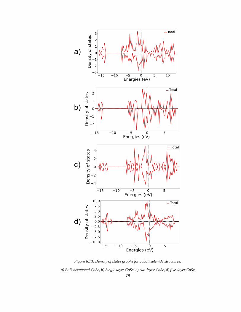
78
Figure 6.13: Density of states graphs for cobalt selenide structures.
a) Bulk hexagonal CoSe, b) Single layer CoSe, c) two-layer CoSe, d) five-layer CoSe.
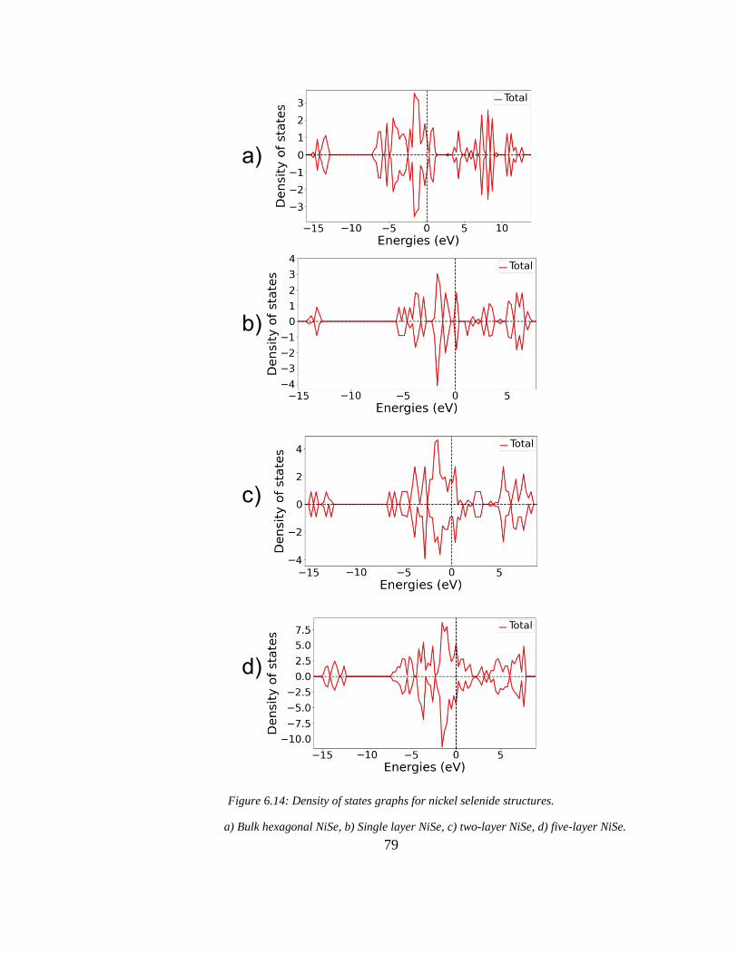
79
Figure 6.14: Density of states graphs for nickel selenide structures.
a) Bulk hexagonal NiSe, b) Single layer NiSe, c) two-layer NiSe, d) five-layer NiSe.

80
The use of density functional theory to provide us with information about our TMC thin
films yielded a wealth of information that we have checked against our physical samples.
In terms of the geometric relaxations to the lowest energy unit cells, our studies on XRD
of our samples correlate well enough within the range of that expected. The average
magnetic moment of our samples also highly correlates with the theoretically predicted
values and with those calculated via the Van Vleck paramagnetism equations. The charge
excess in the out of plane direction seen most significantly in cobalt selenide, and to a
lesser extent in nickel selenide charge density maps explain the observed magnetic
density in our samples. And lastly, our samples in testing with a SQuID magnetometer
yielded paramagnetic effects, which match those found in our density of state studies.
81
7 Conclusions and Further Work
The layered transition chalcogenides offer an interesting capability to materials engineers
and materials scientists especially in their capacity for magnetic effects. Our group has
grown many hexagonal thin films of transition metal chalcogenides (TMCs) using atomic
layer deposition (ALD). The primary films that were characterized for this investigation
were cobalt selenide (CoSe) and nickel selenide (NiSe). Non-magnetic characterizations
included optical measurement, AFM, SEM, XRD, XPS, and Raman spectroscopy. In
these non-magnetic characterizations we found our films to be specular, high-quality thin
films of ~25 nm thickness. Of note, Raman spectroscopy showed characteristic layer
height differences in vibrational band intensity which offers some insight on the
mechanical stresses of bonds in layered films. Magnetic characterizations were done via
VSM and were found lacking in resolution so further studies were carried out by SQuID.
The data from SQuID showed paramagnetic response in all of our films, with a larger
response in CoSe than found in NiSe. Calculations performed on the experimental data
using the model for Van Vleck paramagnetism revealed magnetic moments for metal
atoms to be 0.3839 µB for CoSe and 0.2815 µB for NiSe. These films were of roughly the
same layer thickness and volume. The cause of this difference was examined
theoretically using density functional theory. The simulations took into consideration the
data from our physical characterization of the crystalline phase and geometry of our
films, paired with ligand field theory to set initial conditions of the modeled system. DFT
results produced lowest energy geometric states for various thicknesses of the films in
terms of the number of layers. Faux STM images and charge density models showed us a

82
view of the charge distribution differences between CoSe and NiSe, with CoSe having
more unpaired located at terminal locations perpendicular and pointing out of the plane of
the layered film. Magnetic moments determined from the SQuID magnetometry data
produced reasonable agreement with the simulated values. Densities of states were
calculated using DFT and found that the paramagnetic form of both CoSe and NiSe were
the most probable and that the strength of that paramagnetic effect, the difference in spin-
up and spin-down symmetry, was layer dependent. Our findings show that magnetism in
these materials comes from unpaired spins in non-bonding sites and though the DFT
analysis we have done show that for the top layer, it is reasonable that the edge states are
also places for the localization of spin. This mechanism is a good fit to the observed
results in both modeling and physical characterization.
7.1 Findings
NiSe and CoSe are interesting layered hexagonal 2D materials with a high degree of
variability based upon the number of layers in any given specimen. The ability of ALD to
generate highly crystalline films of few layers was shown. These films were found to
have high crystalline purity and polycrystalline growth through various physical
characterizations to be of the desired hexagonal layered phase. Magnetic studies carried
out showed paramagnetic effects that were ~1.4 times stronger in Bohr magnetic moment
in CoSe compared to NiSe of roughly the same layering height after accommodation for
the volumetric differences.
Through DFT calculations, it was shown that with an increase in layers the unit cells of
CoSe and NiSe shift in width and height, with the trend being a wider and flatter unit cell

83
with the addition of more layers. So too, the location of electrons within the unit cells
shift as layer height increases. These shifts are caused by increased repulsive forces in the
lattice with the varied geometry. In the case of bulk materials, it was seen that these shifts
are very stark in that the density of unpaired spin is highly localized to the outer regions
of the unit cell away from the interior bulk region. This effect was most prominent in
CoSe and showed more prominence as the layer height grew from few to many layers.
This effect is also seen in NiSe but does not have the same prominence or lobed
definition.
7.2 Further research
There is always more that can be known about materials and if time, money, and global
pandemic permitted, we would continue our studies of this class of materials as there is
much that it has to offer. Firstly, exfoliation of fresh species of ALD grown films to attain
long range ordered monolayers would be an important step towards fully proving our
characterization. To gain useful information, especially magnetic, from such a small
volume of material would be an interesting and rewarding challenge. The further research
into edge states of polycrystalline films in modeling would also be an interesting avenue
of study. These films as grown have high order but are polycrystalline in nature. Finally,
modeling, and magnetic characterization of heterostructures of TMCs could yield wholly
different outcomes as the possibilities are nearly endless.

84
References
1. Feynman, R. P. There’s plenty of room at the bottom [data storage]. J.
Microelectromech. Syst. 1, 60–66 (1992).
2. Shankland, S. IBM’s 35 atoms and the rise of nanotech. CNET
https://www.cnet.com/news/ibms-35-atoms-and-the-rise-of-nanotech/.
3. Novoselov, K. S. Electric Field Effect in Atomically Thin Carbon Films. Science 306,
666–669 (2004).
4. IBM100 - Scanning Tunneling Microscope. http://www-
03.ibm.com/ibm/history/ibm100/us/en/icons/microscope/ (2012).
5. Xu, X. et al. Ultrafast epitaxial growth of metre-sized single-crystal graphene on
industrial Cu foil. Science Bulletin 62, 1074–1080 (2017).
6. Monday, M. O., May 27, 2019 & PT, 12:01 pm. Honey I Shrunk the Chips: How die
shrinks help make processors more powerful. AppleInsider
https://appleinsider.com/articles/19/05/27/honey-i-shrunk-the-chips-how-die-shrinks-
help-make-processors-more-powerful-by-making-things-smaller.
7. More Moore - The incredible shrinking transistor | Technology Quarterly | The
Economist. https://www.economist.com/technology-quarterly/2016/03/10/the-
incredible-shrinking-transistor.
8. Lee, Changgu. Measurement of the Elastic Properties and Intrinsic Strength of
Monolayer Graphene | Science. https://science.sciencemag.org/content/321/5887/385.
9. Lee, G.-H. et al. High-Strength Chemical-Vapor–Deposited Graphene and Grain
Boundaries. Science 340, 1073–1076 (2013).

85
10. Novoselov, K. S. et al. Room-Temperature Quantum Hall Effect in Graphene.
Science 315, 1379–1379 (2007).
11. Du, X. Approaching ballistic transport in suspended graphene | Nature
Nanotechnology. https://www-nature-com.proxy.lib.pdx.edu/articles/nnano.2008.199.
12. Novoselov, K. S. et al. Two-dimensional gas of massless Dirac fermions in
graphene. Nature 438, 197–200 (2005).
13. Monajjemi, M. Metal-doped graphene layers composed with boron nitride–
graphene as an insulator: a nano-capacitor. J Mol Model 20, 2507 (2014).
14. Hsieh, C.-T., Lee, C.-E., Chen, Y.-F., Chang, J.-K. & Teng, H. Thermal
conductivity from hierarchical heat sinks using carbon nanotubes and graphene
nanosheets. Nanoscale 7, 18663–18670 (2015).
15. Kim, U. et al. A transparent and stretchable graphene-based actuator for tactile
display. Nanotechnology 24, 145501 (2013).
16. Lin, F., Tong, X., Wang, Y., Bao, J. & Wang, Z. M. Graphene oxide liquid
crystals: synthesis, phase transition, rheological property, and applications in
optoelectronics and display. Nanoscale Research Letters 10, 435 (2015).
17. Singh, V. et al. Graphene based materials: Past, present and future. Progress in
Materials Science 56, 1178–1271 (2011).
18. Cassabois, G., Valvin, P. & Gil, B. Hexagonal boron nitride is an indirect
bandgap semiconductor. Nature Photonics 10, 262–266 (2016).

86
19. Ryou, J., Kim, Y.-S., Kc, S. & Cho, K. Monolayer MoS 2 Bandgap Modulation
by Dielectric Environments and Tunable Bandgap Transistors. Scientific Reports 6,
29184 (2016).
20. Hsu, W.-T. et al. Evidence of indirect gap in monolayer WSe 2. Nature
Communications 8, 929 (2017).
21. Son, S., Nunes, J. F., Shin, Y., Lee, J.-H. & Casiraghi, C. The roughening kinetics
of hydrogenated graphene. Sci Rep 8, 1–8 (2018).
22. Sofo, J. O., Chaudhari, A. S. & Barber, G. D. Graphane: a two-dimensional
hydrocarbon. Physical Review B 75, (2007).
23. Savini, G., Ferrari, A. C. & Giustino, F. First-Principles Prediction of Doped
Graphane as a High-Temperature Electron-Phonon Superconductor. Phys. Rev. Lett.
105, 037002 (2010).
24. Sanna, A., Davydov, A., Dewhurst, J. K., Sharma, S. & Flores-Livas, J. A.
Superconductivity in hydrogenated carbon nanostructures. Eur. Phys. J. B 91, 177
(2018).
25. Watanabe, K., Taniguchi, T. & Kanda, H. Direct-bandgap properties and evidence
for ultraviolet lasing of hexagonal boron nitride single crystal. Nat Mater 3, 404–409
(2004).
26. Solozhenko, V. L., Lazarenko, A. G., Petitet, J.-P. & Kanaev, A. V. Bandgap
energy of graphite-like hexagonal boron nitride. Journal of Physics and Chemistry of
Solids 62, 1331–1334 (2001).
87
27. Tongay, S. et al. Thermally driven crossover from indirect toward direct bandgap
in 2D semiconductors: MoSe2 versus MoS2. Nano Lett. 12, 5576–5580 (2012).
28. Gong, S.-J. et al. Electrically induced 2D half-metallic antiferromagnets and spin
field effect transistors. PNAS 115, 8511–8516 (2018).
29. Liu, G.-B., Xiao, D., Yao, Y., Xu, X. & Yao, W. Electronic structures and
theoretical modelling of two-dimensional group-VIB transition metal dichalcogenides.
Chem. Soc. Rev. 44, 2643–2663 (2015).
30. Liu, Q. et al. Tuning Electronic Structure of Bilayer MoS2 by Vertical Electric
Field: A First-Principles Investigation. J. Phys. Chem. C 116, 21556–21562 (2012).
31. Beaujour, J.-M. L., Chen, W., Kent, A. D. & Sun, J. Z. Ferromagnetic resonance
study of polycrystalline Cobalt ultrathin films. Journal of Applied Physics 99, 08N503
(2006).
32. Duong, D. L., Yun, S. J. & Lee, Y. H. van der Waals Layered Materials:
Opportunities and Challenges. ACS Nano 11, 11803–11830 (2017).
33. Huang, B. et al. Layer-dependent ferromagnetism in a van der Waals crystal
down to the monolayer limit. Nature 546, 270–273 (2017).
34. Heine, T. Transition Metal Chalcogenides: Ultrathin Inorganic Materials with
Tunable Electronic Properties. Acc. Chem. Res. 48, 65–72 (2015).
35. Zhou, X.-F. et al. Two-dimensional magnetic boron. Phys. Rev. B 93, 085406
(2016).
88
36. Togo, A., Oba, F. & Tanaka, I. First-principles calculations of the ferroelastic
transition between rutile-type and CaCl2 type SiO2 at high pressures. Phys. Rev. B 78,
134106 (2008).
37. Dickinson, R. G. & Pauling, L. THE CRYSTAL STRUCTURE OF
MOLYBDENITE. J. Am. Chem. Soc. 45, 1466–1471 (1923).
38. Jong, W. F. D. & Willems, H. W. V. Existenz und Struktur der Disulfide NiS2
und CoS2. Zeitschrift für anorganische und allgemeine Chemie 160, 185–189 (1927).
39. Adachi, K., Sato, K. & Takeda, M. Magnetic Properties of Cobalt and Nickel
Dichalcogenide Compounds with Pyrite Structure. J. Phys. Soc. Jpn. 26, 631–638
(1969).
40. Frindt, R. F. Single Crystals of MoS2 Several Molecular Layers Thick. Journal of
Applied Physics 37, 1928–1929 (1966).
41. Pelá, R. R. & Teles, L. K. Spin Transistors vs. Conventional Transistors: What
Are the Benefits? Journal of Superconductivity and Novel Magnetism 23, 61–64
(2010).
42. Saito, Y., Nojima, T. & Iwasa, Y. Highly crystalline 2D superconductors. Nature
Reviews Materials 2, 16094 (2016).
43. Concise encyclopedia of magnetic & superconducting materials. (Pergamon
Press, 1992).
44. Yuan, N. F. Q., Zhou, B. T., He, W.-Y. & Law, K. T. Ising Superconductivity in
Transition Metal Dichalcogenides. arXiv:1605.01847 [cond-mat] (2016).

89
45. Gong, C. et al. Discovery of intrinsic ferromagnetism in two-dimensional van der
Waals crystals. Nature 546, 265–269 (2017).
46. Snoek, J. L. The Weiss-Heisenberg Theory of Ferro-magnetism and a New Rule
Concerning Magnetostriction and Magneto-Resistance. Nature 163, 837–838 (1949).
47. Hund, F. Zur Deutung verwickelter Spektren, insbesondere der Elemente
Scandium bis Nickel. Z. Physik 33, 345–371 (1925).
48. Heisenberg, W. THE MULTIBODY PROBLEM AND RESONANCE IN
QUANTUM MECHANICS-II. 18.
49. Dirac, P. a. M. Note on Exchange Phenomena in the Thomas Atom. Mathematical
Proceedings of the Cambridge Philosophical Society 26, 376–385 (1930).
50. Heisenberg, W. Zur Theorie des Ferromagnetismus. Z. Physik 49, 619–636
(1928).
51. Bitter, F. Block Structure and Ferromagnetism. Phys. Rev. 37, 91–93 (1931).
52. Powell, F. C. & Fowler, R. H. The direction of magnetisation of single
ferromagnetic crystals. Proceedings of the Royal Society of London. Series A,
Containing Papers of a Mathematical and Physical Character 130, 167–181 (1930).
53. Stoner, E. C. Magnetism in the twentieth century. Proceedings of the Physical
Society 42, 358–371 (1930).
54. Vandenberg-Voorhoeve, J. M. Structural and Magnetic Properties of Layered
Chalcogenides of the Transition Elements. in Optical and Electrical Properties 423–
457 (Springer, Dordrecht, 1976). doi:10.1007/978-94-010-1478-6_8.

90
55. Richardson, D. D. A calculation of Van der Waals interactions in and between
layers of atoms: application to graphite. J. Phys. C: Solid State Phys. 10, 3235–3242
(1977).
56. Mandale, A. B., Badrinarayanan, S., Date, S. K. & Sinha, A. P. B. Photoelectron-
spectroscopic study of nickel, manganese and cobalt selenides. Journal of Electron
Spectroscopy and Related Phenomena 33, 61–72 (1984).
57. Structural phase transitions in layered transition metal compounds. (D. Reidel
Pub. Co. ; Sold and distributed in the U.S.A. and Canada by Kluwer Academic
Publishers, 1986).
58. Saiki, K., Ueno, K., Shimada, T. & Koma, A. Application of Van der Waals
epitaxy to highly heterogeneous systems. Journal of Crystal Growth 95, 603–606
(1989).
59. Campos, C. E. M. et al. Hexagonal CoSe formation in mechanical alloyed
Co75Se25 mixture. Solid State Communications 131, 265–270 (2004).
60. Gruyters, M. Cobalt oxide/ferromagnet bilayers: Exchange coupling and
dominance of the antiferromagnet. EPL 64, 803 (2003).
61. Zhao, J.-F. et al. Graphene-like cobalt selenide nanostructures: template-free
solvothermal synthesis, characterization and wastewater treatment. CrystEngComm 13,
5681 (2011).
62. Moloto, N., Moloto, M. J., Coville, N. J. & Sinha Ray, S. Synthesis and
characterization of nickel selenide nanoparticles: size and shape determining
parameters. Journal of Crystal Growth 324, 41–52 (2011).
91
63. T. Swesi, A., Masud, J. & Nath, M. Nickel selenide as a high-efficiency catalyst
for oxygen evolution reaction. Energy & Environmental Science 9, 1771–1782 (2016).
64. Buchmaier, C. et al. Nickel sulfide thin films and nanocrystals synthesized from
nickel xanthate precursors. J Mater Sci 52, 10898–10914 (2017).
65. Schwartz, R. W., Schneller, T. & Waser, R. Chemical solution deposition of
electronic oxide films. Comptes Rendus Chimie 7, 433–461 (2004).
66. Wang, C. C., Zaininger, K. H. & Duffy, M. T. VAPOR DEPOSITION AND
CHARACTERIZATION OF METAL OXIDE THIN FILMS FOR ELECTRONIC
APPLICATIONS. RCA Rev. 31: 728-41(Dec 1970). (1970).
67. Kuan, T. S., Kuech, T. F., Wang, W. I. & Wilkie, E. L. Long-Range Order in
Al_xGa_(1-x)As. Phys. Rev. Lett. 54, 201–204 (1985).
68. Puurunen, R. L. A Short History of Atomic Layer Deposition: Tuomo Suntola’s
Atomic Layer Epitaxy: A Short History of Atomic Layer. Chemical Vapor Deposition
20, 332–344 (2014).
69. Merkx, M. J. M., Sandoval, T. E., Hausmann, D. M., Kessels, W. M. M. &
Mackus, A. J. M. Mechanism of Precursor Blocking by Acetylacetone Inhibitor
Molecules during Area-Selective Atomic Layer Deposition of SiO2. Chem. Mater. 32,
3335–3345 (2020).
70. Silvennoinen, R. J. et al. Atomic layer deposition of iridium(III) acetylacetonate
on alumina, silica–alumina, and silica supports. Applied Surface Science 253, 4103–
4111 (2007).

92
71. Górka-Kostrubiec, B. & Szczepaniak-Wnuk, I. Magnetic study of a mixture of
magnetite and metallic iron in indoor dust samples. Air Qual Atmos Health 10, 105–
116 (2017).
72. Szczepaniak-Wnuk, I. & Górka-Kostrubiec, B. Magnetic particles in indoor dust
as marker of pollution emitted by different outside sources. Stud Geophys Geod 60,
297–315 (2016).
73. Chady, S. Analysis of iron nanoparticles in organic solvents used in the
semiconductor industry using single particle ICP-MS in reaction mode.
https://www.perkinelmer.com/lab-solutions/resources/docs/Nanomaterials_SP-ICP-
MS_Compendium(012982_01).pdf (2015).
74. Friedrich, W., Knipping, P. & Laue, M. Interferenzerscheinungen bei
Röntgenstrahlen. Annalen der Physik 346, 971–988 (1913).
75. Dong, J. et al. Cobalt selenide nanorods used as a high efficient counter electrode
for dye-sensitized solar cells. Electrochimica Acta 168, 69–75 (2015).
76. Sobhani, A. & Salavati-Niasari, M. Cobalt selenide nanostructures: Hydrothermal
synthesis, considering the magnetic property and effect of the different synthesis
conditions. Journal of Molecular Liquids 219, 1089–1094 (2016).
77. Panneerselvam, A., Malik, Mohammad. A., Afzaal, M., O’Brien, P. & Helliwell,
M. The Chemical Vapor Deposition of Nickel Phosphide or Selenide Thin Films from
a Single Precursor. J. Am. Chem. Soc. 130, 2420–2421 (2008).
78. Hopkins, M. A., Kuperman, N., Barnes, J. & Solanki, R. Magnetic
Characterization of Cobalt Selenide and Nickel Selenide Thin Films. in 2018 IEEE
93
13th Nanotechnology Materials and Devices Conference (NMDC) 1–4 (2018).
doi:10.1109/NMDC.2018.8605836.
79. Ding, K. et al. Phase-change heterostructure enables ultralow noise and drift for
memory operation. Science 366, 210–215 (2019).
80. Tran, K. et al. Evidence for moiré excitons in van der Waals heterostructures.
Nature 567, 71–75 (2019).
81. Bennett, L. H. Electronic Density of States: Based on Invited and Contributed
Papers and Discussion. (U.S. National Bureau of Standards, 1971).
82. Winter, H., Durham, P. J., Temmerman, W. M. & Stocks, G. M. Electronic
density of states and the x-ray photoelectron spectra of the valence band of Cu-Pd
alloys. Phys. Rev. B 33, 2370–2379 (1986).
83. Fadley, C. S. & Shirley, D. A. Electronic densities of states from x-ray
photoelectron spectroscopy. J. RES. NATL. BUR. STAN. SECT. A. 74A, 543 (1970).
84. Grosvenor, A. P., Biesinger, M. C., Smart, R. St. C. & McIntyre, N. S. New
interpretations of XPS spectra of nickel metal and oxides. Surface Science 600, 1771–
1779 (2006).
85. Hagelin-Weaver, H. A. E., Weaver, J. F., Hoflund, G. B. & Salaita, G. N.
Electron energy loss spectroscopic investigation of Ni metal and NiO before and after
surface reduction by Ar+ bombardment. Journal of Electron Spectroscopy and Related
Phenomena 134, 139–171 (2004).
94
86. Kirubasankar, B. et al. In situ grown nickel selenide on graphene nanohybrid
electrodes for high energy density asymmetric supercapacitors. Nanoscale 10, 20414–
20425 (2018).
87. Kolobov, A. V. & Tominaga, J. Two-Dimensional Transition-Metal
Dichalcogenides. vol. 239 (Springer International Publishing, 2016).
88. Buscema, M., Steele, G. A., van der Zant, H. S. J. & Castellanos-Gomez, A. The
effect of the substrate on the Raman and photoluminescence emission of single-layer
MoS2. Nano Res. 7, 561–571 (2014).
89. Wang, X. H., Zheng, C. C. & Ning, J. Q. Influence of curvature strain and Van
der Waals force on the inter-layer vibration mode of WS 2 nanotubes: A confocal
micro-Raman spectroscopic study. Sci Rep 6, 1–6 (2016).
90. Saito, R., Tatsumi, Y., Huang, S., Ling, X. & Dresselhaus, M. S. Raman
spectroscopy of transition metal dichalcogenides. J. Phys.: Condens. Matter 28,
353002 (2016).
91. Park, J., Kim, Y., Jhon, Y. I. & Jhon, Y. M. Temperature dependent Raman
spectroscopic study of mono-, bi-, and tri-layer molybdenum ditelluride. Appl. Phys.
Lett. 107, 153106 (2015).
92. Molina-Sánchez, A. & Wirtz, L. Phonons in single-layer and few-layer MoS2 and
WS2. Phys. Rev. B 84, 155413 (2011).
93. Campos, C. E. M., de Lima, J. C., Grandi, T. A., Machado, K. D. & Pizani, P. S.
Structural studies of cobalt selenides prepared by mechanical alloying. Physica B:
Condensed Matter 324, 409–418 (2002).

95
94. Kukunuri, S., Reshma Krishnan, M. & Sampath, S. The effect of structural
dimensionality on the electrocatalytic properties of the nickel selenide phase. Physical
Chemistry Chemical Physics 17, 23448–23459 (2015).
95. Bloch, F. Zur Theorie des Ferromagnetismus. Z. Physik 61, 206–219 (1930).
96. Peierls, R. Bemerkungen über Umwandlungstemperaturen. (1934)
doi:10.5169/SEALS-110415.
97. Landau, L. Theory of phase transformations ii. (Eksp. Teor. Fiz. Phys. Z., 1937).
98. Schreiber, F. http://www.soft-matter.uni-
tuebingen.de/teaching/MerminWagnerVorlesungWiSe07-08.pdf.
99. Back, C. H. et al. Experimental confirmation of universality for a phase transition
in two dimensions. Nature 378, 597–600 (1995).
100. MacNeill, D. et al. Breaking of Valley Degeneracy by Magnetic Field in
Monolayer MoSe2. Phys. Rev. Lett. 114, 037401 (2015).
101. Magnetic Moments of Transition Metals. Chemistry LibreTexts
https://chem.libretexts.org/Core/Inorganic_Chemistry/Crystal_Field_Theory/Magnetic
_Moments_of_Transition_Metals (2014).
102. Van Vleck, J. H. The theory of electric and magnetic susceptibilities. (Oxford
University Press, 1965).
103. Wilson, J. A. & Yoffe, A. D. The transition metal dichalcogenides discussion and
interpretation of the observed optical, electrical and structural properties. Advances in
Physics 18, 193 (1969).

96
104. Martin, J. L. & Takats, J. Trigonal prismatic versus octahedral coordination
geometry of transition metal dithiolates: Comparison between saturated and
unsaturated early transition metal tris(1,2-dithiolate) complexes. Can. J. Chem. 67,
1914–1923 (1989).
105. Blocker, T. G., Simmons, C. L. & West, F. G. Magnetic Properties of the Oxygen
Molecule in Solid Oxygen‐Argon Mixtures. Journal of Applied Physics 40, 1154–1155
(1969).
106. Emergent phenomena in correlated matter: lecture notes of the Autumn School
Correlated Electrons 2013 at Forschungszentrum Jülich, 23 – 27 September 2013.
(Forschungszentrum Jülich, 2013).
107. Bersuker, I. B. Electronic structure and properties of transition metal
compounds: introduction to the theory. (Wiley, 2010).
108. Margenau, H. & Kestner, N. R. Theory of intermolecular forces. (Pergamon
Press, 1971).
109. Crick, F. What mad pursuit: a personal view of scientific discovery. (Basic Books,
1988).
110. Hartree, D. R. & Hartree, W. Self-consistent field, with exchange, for beryllium.
Proceedings of the Royal Society of London. Series A - Mathematical and Physical
Sciences 150, 9–33 (1935).
111. Vanpoucke, D. E. P. & Brocks, G. Formation of Pt-induced Ge atomic nanowires
on Pt/Ge(001): A density functional theory study. Phys. Rev. B 77, 241308 (2008).
97
112. Becke, A. D. & Johnson, E. R. Exchange-hole dipole moment and the dispersion
interaction revisited. J. Chem. Phys. 127, 154108 (2007).
113. Corminboeuf, C. Minimizing Density Functional Failures for Non-Covalent
Interactions Beyond van der Waals Complexes. Acc. Chem. Res. 47, 3217–3224
(2014).
114. Materials Project. https://materialsproject.org/.
115. Garg, P., Adlakha, I. & Solanki, K. N. Effect of solutes on ideal shear resistance
and electronic properties of magnesium: A first-principles study. Acta Materialia 153,
327–335 (2018).
116. Britney Spears’ Guide to Semiconductor Physics: Density of States.
http://britneyspears.ac/physics/dos/dos.htm.
117. Lipton, D. & Jacobs, R. L. The density of states and magnetic parameters for
transition metals. J. Phys. C: Solid State Phys. 3, S389–S396 (1970).
118. Zhou, X. et al. Metastable Layered Cobalt Chalcogenides from Topochemical
Deintercalation. J. Am. Chem. Soc. 138, 16432–16442 (2016).
119. drga, josef. (6) (PDF) DENSITY OF STATES AND MAGNETIC PROPERTIES
OF Al2O3 , Cr2O3 AND CrO2. ResearchGate
https://www.researchgate.net/publication/279524787_DENSITY_OF_STATES_AND
_MAGNETIC_PROPERTIES_OF_Al2O3_Cr2O3_AND_CrO2.
120. Lewis, S. P., Allen, P. B. & Sasaki, T. Band structure and transport properties of
CrO2. Phys. Rev. B 55, 10253–10260 (1997).