Inverter and PFC Reference Design - TI.com
90
Design Guide: TIDA-01606 10-kW, Bidirectional Three-Phase Three-Level (T-type) Inverter and PFC Reference Design Description This reference design provides an overview on how to implement a bidirectional three-level, three-phase, SiC-based active front end (AFE) inverter and PFC stage. The design uses a switching frequency of 50 kHz and a LCL output filter to reduce the size of the magnetics. A peak efficiency of 99% is achieved. The design shows how to implement a complete three phase AFE control in the DQ domain. The control and software is validated on the actual hardware and on hardware in the loop (HIL) setup. Resources TIDA-01606 Design Folder TMS320F28379D Product Folder C2000WARE-DIGITALPOWER-SDK Tool Folder ISO5852S, UCC5320 Product Folder TMDSCNCD28379D Tool Folder AMC1306M05, OPA4340 Product Folder LM76003, PTH08080W Product Folder TLV1117LV, OPA350 Product Folder UCC27211 Product Folder Ask our TI E2E ™ support experts Features • Rated nominal and maximum input voltage at 800- V and 1000-V DC, Max Power 10-kW/10-kVA at 400-V AC L-L 50 or 60 Hz • Compact output LCL filter with switching frequency of 50 kHz • < 2% output current THD at full load • Isolated driver ISO5852S with reinforced isolation for driving high-voltage SiC MOSFET and UCC5320S for driving middle Si IGBT • Isolated current sensing using AMC1301 for load current monitoring • TMS320F28379D control card for digital control with Trignometric Math Unit (TMU) to accelerate PLL computation, comparator sub-system for protection implementation and Control Law Accelerator (CLA) to offload the control loops to the co-processor. Applications • String inverter • Central inverter • On-board (OBC) and wireless charger • DC charging (pile) station • Portable DC charger • Energy storage power conversion system (PCS) G3 G4 G7 G8 G11 G12 G1 G5 G9 G2 G6 G10 la lb lc Vinverter Iout Vgrid OPA4340 OPA4350 x3 AMC1306 Iout Vgrid Vinverter lc lb la F28377D Control Card PWM x12 RST FLT ISO5852 x2 UCC5352 x2 UCC27211 SN74LVC126APWR Reset TLV1117 SN6505B LM76003 12 V 15-60 VIN G9, 10, 11, 12 G5, 6, 7, 8 G1, 2, 3, 4 LCL Filter Hall Sensor x3 Shunt x3 DC Link Input Si/ SiC (Low Frequency) SiC MOSFET (High Frequency) www.ti.com Description TIDUE53F – MARCH 2018 – REVISED SEPTEMBER 2021 Submit Document Feedback 10-kW, Bidirectional Three-Phase Three-Level (T-type) Inverter and PFC Reference Design 1 Copyright © 2021 Texas Instruments Incorporated
Transcript of Inverter and PFC Reference Design - TI.com

Design Guide: TIDA-0160610-kW, Bidirectional Three-Phase Three-Level (T-type) Inverter and PFC Reference Design
DescriptionThis reference design provides an overview on how to implement a bidirectional three-level, three-phase, SiC-based active front end (AFE) inverter and PFC stage. The design uses a switching frequency of 50 kHz and a LCL output filter to reduce the size of the magnetics. A peak efficiency of 99% is achieved. The design shows how to implement a complete three phase AFE control in the DQ domain. The control and software is validated on the actual hardware and on hardware in the loop (HIL) setup.
ResourcesTIDA-01606 Design Folder
TMS320F28379D Product Folder
C2000WARE-DIGITALPOWER-SDK Tool Folder
ISO5852S, UCC5320 Product FolderTMDSCNCD28379D Tool FolderAMC1306M05, OPA4340 Product FolderLM76003, PTH08080W Product FolderTLV1117LV, OPA350 Product FolderUCC27211 Product Folder
Ask our TI E2E™ support experts
Features• Rated nominal and maximum input voltage at 800-
V and 1000-V DC, Max Power 10-kW/10-kVA at 400-V AC L-L 50 or 60 Hz
• Compact output LCL filter with switching frequency of 50 kHz
• < 2% output current THD at full load• Isolated driver ISO5852S with reinforced isolation
for driving high-voltage SiC MOSFET and UCC5320S for driving middle Si IGBT
• Isolated current sensing using AMC1301 for load current monitoring
• TMS320F28379D control card for digital control with Trignometric Math Unit (TMU) to accelerate PLL computation, comparator sub-system for protection implementation and Control Law Accelerator (CLA) to offload the control loops to the co-processor.
Applications• String inverter• Central inverter• On-board (OBC) and wireless charger• DC charging (pile) station• Portable DC charger• Energy storage power conversion system (PCS)
G3 G4
G7 G8
G11 G12
G1 G5 G9
G2
G6 G10
la
lb
lc
Vinverter
Iout
Vgrid
OPA4340
OPA4350
x3
AMC1306Iout
Vgrid
Vinverter
lc
lb
la
F28377D
Control Card
PWM x12
RST
FLT
ISO5852 x2 UCC5352 x2
UCC27211 SN74LVC126APWR Reset TLV1117
SN6505B
LM76003
12 V
15-60 VIN
G9, 10, 11, 12G5, 6, 7, 8G1, 2, 3, 4
LCL FilterHall Sensor x3 Shunt x3
DC Link
Input
Si/ SiC
(Low Frequency)
SiC MOSFET
(High Frequency)
www.ti.com Description
TIDUE53F – MARCH 2018 – REVISED SEPTEMBER 2021Submit Document Feedback
10-kW, Bidirectional Three-Phase Three-Level (T-type) Inverter and PFC Reference Design
1
Copyright © 2021 Texas Instruments Incorporated

1 System DescriptionModern commercial scale solar inverters are seeing innovation on two fronts, which lead to smaller, higher efficiency products on the market:
• The move to higher voltage solar arrays• Reducing the size of the onboard magnetics
By increasing the voltage to 1000-V or 1500-V DC from the array, the current can be reduced to maintain the same power levels. This reduction in current results in less copper and smaller power conducting devices required in the design. The reduction in di/dt also reduces the stress on electrical components. However, sustained DC voltages of > 1 kV can be difficult to design to, or even find components that can survive it.
To compensate for the voltage stresses generated by high-voltage solar arrays, new topologies of solar inverters have been designed. Traditional half bridges block the full input voltage on each switching device. By adding additional switched blocking and conduction components, the overall stress on the device can be significantly reduced. This reference design shows how to implement a three-level converter. Higher level converters are also possible, further increasing the voltage handling capability.
Additional power density in solar electronics is also being enabled by moving to higher switching speeds in the power converters. As this design shows, even a modestly higher switching speed reduces the overall size requirement of the output filter stage—a primary contributor to the design size.
Traditional switching devices have a limit in how quickly they can switch high voltages, or more appropriately, the dV/dt ability of the device. This slow ramp up and down increases conduction loss because the device spends more time in a switching state. This increased switch time also increases the amount of dead time required in the control system to prevent shoot-through and shorts. The solution to this has been developed in newer switching semiconductor technology like SiC and GaN devices with high electron mobility. This reference design uses SiC MOSFETs alongside TI's SiC gate driver technology to demonstrate the potential increase in power density.
Similarly for Onboard Chargers (OBC) higher power chargers (11 kW and 22 kW) are increasingly required. For which three phase PFC is necessary, this design shows implementation of three phase PFC using DQ control and presents the complete control loop model.
1.1 Key System SpecificationsTable 1-1. Key System Specifications
PARAMETER SPECIFICATIONS DETAILSOutput power 10 kW Section 2.3
Output voltage Three-phase 400-V AC Section 2.3
Output frequency 50 or 60 Hz Section 2.3
Output current 18 A (max) Section 2.3
Nominal input voltage 800-V DC Section 2.3
Input voltage range 600-V to 1000-V DC Section 2.3
Inverter switching frequency 50 kHz Section 2.3
Efficiency 99% Section 2.3.1.5
Power density 1 kW/L+
System Description www.ti.com
2 10-kW, Bidirectional Three-Phase Three-Level (T-type) Inverter and PFC Reference Design
TIDUE53F – MARCH 2018 – REVISED SEPTEMBER 2021Submit Document Feedback
Copyright © 2021 Texas Instruments Incorporated

2 System Overview2.1 Block Diagram
Figure 2-1. TIDA-01606 Block Diagram
This reference design is comprised of four separate boards that intercommunicate. The following boards work
in tandem to form this three-phase inverter reference design:
• A power board, comprising all of the switching device, LCL filter, sensing electronics, and power structure• A TMS320F28379D Control Card to support the DSP• Three gate driver cards, each with two ISO5852S and two UCC5320 gate drivers• A DC bus voltage measuring board (TIDA-01606 ISOHVCARD)
2.2 Highlighted Products2.2.1 ISO5852S
The ISO5852S device is a 5.7-kVRMS, reinforced isolated gate driver for IGBTs and MOSFETs with split outputs, OUTH and OUTL, providing 2.5-A source and 5-A sink current. The input side operates from a single 2.25-V to 5.5-V supply. The output side allows for a supply range from minimum 15 V to maximum 30 V. Two complementary CMOS inputs control the output state of the gate driver. The short propagation time of 76 ns provides accurate control of the output stage.
• 100-kV/μs minimum common-mode transient immunity (CMTI) at VCM = 1500 V• Split outputs to provide 2.5-A peak source and 5-A peak sink currents• Short propagation delay: 76 ns (typ), 110 ns (max)• 2-A active Miller clamp• Output short-circuit clamp• Soft turnoff (STO) during short circuit• Fault alarm upon desaturation detection is signaled on FLT and reset through RST• Input and output undervoltage lockout (UVLO) with Ready (RDY) pin indication• Active output pulldown and default low outputs with low supply or floating inputs• 2.25-V to 5.5-V input supply voltage• 15-V to 30-V output driver supply voltage
www.ti.com System Overview
TIDUE53F – MARCH 2018 – REVISED SEPTEMBER 2021Submit Document Feedback
10-kW, Bidirectional Three-Phase Three-Level (T-type) Inverter and PFC Reference Design
3
Copyright © 2021 Texas Instruments Incorporated

• CMOS compatible inputs• Rejects input pulses and noise transients shorter than 20 ns• Operating temperature: –40°C to +125°C ambient• Isolation surge withstand voltage of 12800-VPK
GND1 VEE2
RST
RDY
FLT
IN+
IN±
VCC1 VCC2
DESAT
GND2
OUTH
OUTL
CLAMP
VCC1
VCC1
UVLO1
Mute
DecoderQ S
RQ
VCC1
VCC1
Gate Drive
and
Encoder Logic
UVLO2
2 V
9 V
500 µA
STO
VCC2
Ready
Fault
Figure 2-2. ISO5852S Functional Block Diagram
2.2.2 UCC5320
The UCC53x0 is a family of compact, single-channel, isolated IGBT, SiC, and MOSFET gate drivers with superior isolation ratings and variants for pinout configuration, and drive strength.
The UCC53x0 is available in an 8-pin SOIC (D) package. This package has a creepage and clearance of 4 mm and can support isolation voltage up to 3 kVRMS, which is good for applications where basic isolation is needed. With these various options and wide power range, the UCC53x0 family is a good fit for motor drives and industrial power supplies.
• 3-V to 15-V input supply voltage• 13.2-V to 33-V output driver supply voltage• Feature options:
– Split outputs (UCC5320S and UCC5390S)– UVLO with respect to IGBT emitter (UCC5320E and UCC5390E)– Miller clamp option (UCC5310M and UCC5350M)
• Negative 5-V handling capability on input pins• 60-ns (typical) propagation delay for UCC5320S, UCC5320E, and UCC5310M• 100-kV/µs minimum CMTI• Isolation surge withstand voltage: 4242 VPK• Safety-related certifications:
– 4242-VPK isolation per DIN V VDE V 0884-10 and DIN EN 61010-1 (planned)– 3000-VRMS isolation for 1 minute per UL 1577 (planned)– CSA Component Acceptance Notice 5A, IEC 60950-1 and IEC 61010-1 End Equipment Standards
(Planned)– CQC Certification per GB4943.1-2011 (Planned)
System Overview www.ti.com
4 10-kW, Bidirectional Three-Phase Three-Level (T-type) Inverter and PFC Reference Design
TIDUE53F – MARCH 2018 – REVISED SEPTEMBER 2021Submit Document Feedback
Copyright © 2021 Texas Instruments Incorporated

• 4-kV ESD on all pins• CMOS inputs• 8-pin narrow body SOIC package• Operating temperature: –40°C to +125°C ambient
text
VCC2
UVLO,
Level
Shift
and
Control
Logic
VCC2
VOUTH
IN±
IN+
VOUTL
VCC1
VEE2GND1
ISO
LA
TIO
N B
AR
RIE
R
UVLO
and
Input
Logic
15 V
Rest of
Circuit
5 V
Figure 2-3. UCC5320 Functional Block Diagram (S Version)
2.2.3 TMS320F28379D
The Delfino™ TMS320F2837xD is a powerful 32-bit floating-point microcontroller unit (MCU) designed for advanced closed-loop control applications such as industrial drives and servo motor control; solar inverters and converters; digital power; transportation; and power line communications. Complete development packages for digital power and industrial drives are available as part of the powerSUITE and DesignDRIVE initiatives. While the Delfino product line is not new to the TMS320C2000™ portfolio, the F2837xD supports a new dual-core C28x architecture that significantly boosts system performance. The integrated analog and control peripherals also let designers consolidate control architectures and eliminate multiprocessor use in high-end systems.
• Dual-core architecture:– Two TMS320C28x 32-bit CPUs– 200 MHz– IEEE 754 single-precision floating-point unit (FPU)– Trigonometric math unit (TMU)– Viterbi/complex math unit (VCU-II)
• Two programmable control law accelerators (CLAs)– 200 MHz– IEEE 754 single-precision floating-point instructions– Executes code independently of main CPU
• On-chip memory– 512KB (256 kW) or 1MB (512 kW) of Flash (ECC-protected)– 172KB (86 kW) or 204KB (102 kW) of RAM (ECC-protected or parity-protected)– Dual-zone security supporting third-party development
• Clock and system control:– Two internal zero-pin 10-MHz oscillators– On-chip crystal oscillator– Windowed watchdog timer module– Missing clock detection circuitry
• 1.2-V core, 3.3-V I/O design• System peripherals:
– Two external memory interfaces (EMIFs) with ASRAM and SDRAM support– Dual six-channel direct memory access (DMA) controllers
www.ti.com System Overview
TIDUE53F – MARCH 2018 – REVISED SEPTEMBER 2021Submit Document Feedback
10-kW, Bidirectional Three-Phase Three-Level (T-type) Inverter and PFC Reference Design
5
Copyright © 2021 Texas Instruments Incorporated

– Up to 169 individually programmable, multiplexed general-purpose input/output (GPIO) pins with input filtering
– Expanded peripheral interrupt controller (ePIE)– Multiple low-power mode (LPM) support with external wakeup
• Communications peripherals:– USB 2.0 (MAC + PHY)– Support for 12-pin 3.3-V compatible universal parallel port (uPP) interface– Two controller area network (CAN) modules (pin-bootable)– Three high-speed (up to 50-MHz) SPI ports (pin-bootable)– Two multichannel buffered serial ports (McBSPs)– Four serial communications interfaces (SCI/UART) (pin-bootable)– Two I2C interfaces (pin-bootable)
• Analog subsystem:– Up to four analog-to-digital converters (ADCs):
• 16-bit mode– 1.1 MSPS each (up to 4.4-MSPS system throughput)– Differential inputs– Up to 12 external channels
• 12-bit mode– 3.5 MSPS each (up to 14-MSPS system throughput)– Single-ended inputs– Up to 24 external channels
• Single sample-and-hold (S/H) on each ADC• Hardware-integrated post-processing of ADC conversions:
– Saturating offset calibration– Error from setpoint calculation– High, low, and zero-crossing compare, with interrupt capability– Trigger-to-sample delay capture
– Eight windowed comparators with 12-bit digital-to-analog converter (DAC) references– Three 12-bit buffered DAC outputs
• Enhanced control peripherals:– 24 pulse width modulator (PWM) channels with enhanced features– 16 high-resolution pulse width modulator (HRPWM) channels:
• High resolution on both A and B channels of eight PWM modules• Dead-band support (on both standard and high resolution)
– Six enhanced capture (eCAP) modules– Three enhanced quadrature encoder pulse (eQEP) modules– Eight sigma-delta filter module (SDFM) input channels, two parallel filters per channel:
• Standard SDFM data filtering• Comparator filter for fast action for out of range
System Overview www.ti.com
6 10-kW, Bidirectional Three-Phase Three-Level (T-type) Inverter and PFC Reference Design
TIDUE53F – MARCH 2018 – REVISED SEPTEMBER 2021Submit Document Feedback
Copyright © 2021 Texas Instruments Incorporated

16-/12-bit ADC
x4
Analog
MUX
ADC
Result
Regs
Peripheral Frame 1
Global Shared
16x 4Kx16
GS0-GS15 RAMs
CPU1 to CPU2
1Kx16 MSG RAM
GPIO MUX, Input X-BAR, Output X-BAR
CPU1.M0 RAM 1Kx16
CPU1.M1 RAM 1Kx16
CPU2.M0 RAM 1Kx16
CPU2.M1 RAM 1Kx16
PSWDPSWD
Secure Memories
shown in Red
MEMCPU2
CPU2 to CPU1
1Kx16 MSG RAM
MEMCPU1
CPU1 Buses
CPU2 Buses
A5:0
B5:0
C5:2
ADCIN14
ADCIN15
D5:0
Comparator
Subsystem
(CMPSS)
DAC
x3
Config
CP
U1.C
LA
1B
us
CP
U2
.CL
A1
Bu
s
C28 CPU-1FPU
VCU-II
TMU
CPU Timer 0
CPU Timer 1
CPU Timer 2
ePIE(up to 192
interrupts)
WD Timer
NMI-WDT
C28 CPU-2FPU
VCU-II
TMU
CPU Timer 0
CPU Timer 1
CPU Timer 2
ePIE(up to 192
interrupts)
WD Timer
NMI-WDTCPU1.CLA1 Data ROM
(4Kx16)
CPU1.CLA1 to CPU1
128x16 MSG RAM
CPU1 to CPU1.CLA1
128x16 MSG RAM
CPU1.D0 RAM 2Kx16
CPU1.D1 RAM 2Kx16
Boot-ROM 32Kx16
Nonsecure
Secure-ROM 32Kx16
Secure
CPU1 Local Shared
6x 2Kx16
LS0-LS5 RAMs
CPU2 to CPU2.CLA1
128x16 MSG RAM
CPU2.CLA1 to CPU2
128x16 MSG RAM
CPU2.D0 RAM 2Kx16
CPU2.D1 RAM 2Kx16
CPU2.CLA1 Data ROM
(4Kx16)
Boot-ROM 32Kx16
Nonsecure
Secure-ROM 32Kx16
Secure
CPU2 Local Shared
LS0-LS5 RAMs
CPU1.CLA1
CPU1.DMA CPU2.DMA
CPU2.CLA1
Data BusBridge
ePWM-1/../12eCAP-
1/../6eQEP-1/2/3 SDFM-1/2
EX
TS
YN
CIN
EX
TS
YN
CO
UT
TZ
1-T
Z6
EC
AP
x
EQ
EP
xA
EQ
EP
xB
EP
WM
xA
EP
WM
xB
EQ
EP
xI
EQ
EP
xS
SD
x_
Dy
SD
x_
Cy
A
B
C
D
JTAG
AUXCLKIN
External Crystal orOscillator
Watchdog 1/2
Main PLL
Aux PLL
INTOSC1
INTOSC2
Low-PowerMode Control
GPIO MUX
TRST
TCK
TDI
TMS
TDO
6x 2Kx16
DualCode
SecurityModule
+Emulation
CodeSecurity
Logic(ECSL)
DualCode
SecurityModule
+Emulation
CodeSecurity
Logic(ECSL)
InterprocessorCommunication
(IPC)Module
PUMP
OTP/Flash
Wrapper
FLASH256K x 16
Secure
UserConfigurable
DCSMOTP
1K x 16
OTP/Flash
Wrapper
FLASH256K x 16
Secure
UserConfigurable
DCSMOTP
1K x 16
SCI-
A/B/C/D
(16L FIFO)
I2C-A/B
(16L FIFO)
Data Bus Bridge
SC
ITX
Dx
SC
IRX
Dx
SD
Ax
SC
Lx
CAN-
A/B(32-MBOX)
Data BusBridge
CA
NR
Xx
CA
NT
Xx
GPIO
Data BusBridge
GP
IOn
Data BusBridge
USB
Ctrl /
PHY
US
BD
P
US
BD
M
USB
Ctrl /
PHY
EMIF1
Data BusBridge
EM
1D
x
EM
1A
x
EM
1C
TL
x
EMIF2
Data BusBridge
EM
2D
x
EM
2A
x
EM
2C
TL
x
Peripheral Frame 2
SPI-
A/B/C
(16L FIFO)
SP
ISIM
Ox
SP
ISO
MIx
SP
ICL
Kx
SP
IST
Ex
McBSP-
A/B
MD
Xx
MD
Rx
MC
LK
Xx
MC
LK
Rx
MF
SX
x
MF
SR
x
uPPRAM
UP
PA
D[7
:0]
UP
PA
EN
UP
PA
ST
UP
PA
WT
UP
PA
CL
K
HRPWM-1/../8(CPU1 only)
Figure 2-4. TMS320F28379D Functional Block Diagram
2.2.4 AMC1305M05
The AMC1305 device is a precision, delta-sigma (ΔΣ) modulator with the output separated from the input circuitry by a capacitive double isolation barrier that is highly resistant to magnetic interference. This barrier is certified to provide reinforced isolation of up to 7000 VPEAK according to the DIN V VDE V 0884-10, UL1577, and CSA standards. Used in conjunction with isolated power supplies, the device prevents noise currents on a high common-mode voltage line from entering the local system ground and interfering with or damaging low voltage circuitry.
• Pin-compatible family optimized for shunt-resistor-based current measurements:– ±50-mV or ±250-mV input voltage ranges– CMOS or LVDS digital interface options
• Excellent DC performance supporting high-precision sensing on system level:– Offset error: ±50 µV or ±150 µV (max)– Offset drift: 1.3 µV/°C (max)– Gain error: ±0.3% (max)– Gain drift: ±40 ppm/°C (max)
• Safety-related certifications:– 7000-VPK reinforced isolation per DIN V VDE V 0884-10 (VDE V 0884-10): 2006-12– 5000-VRMS isolation for 1 minute per UL1577– CAN/CSA No. 5A-Component Acceptance Service Notice, IEC 60950-1, and IEC 60065 End Equipment
Standards• Transient immunity: 15 kV/µs (min)• High electromagnetic field immunity (see ISO72x Digital Isolator Magnetic-Field Immunity )• External 5-MHz to 20-MHz clock input for easier system-level synchronization
www.ti.com System Overview
TIDUE53F – MARCH 2018 – REVISED SEPTEMBER 2021Submit Document Feedback
10-kW, Bidirectional Three-Phase Three-Level (T-type) Inverter and PFC Reference Design
7
Copyright © 2021 Texas Instruments Incorporated

• Fully specified over the extended industrial temperature range
DOUT
CLKIN
DVDD
DGNDAGND
AINP
AINN
AVDD
AMC1305
HV+
HV-
To Load
Floating
Power Supply
SD-Cx
SD-Dx
TMS320F2837x
3.3 V, or 5.0 V
Gate Driver
Gate Driver
5.0 V
Re
info
rce
d Iso
latio
n
PWMx
RSHUNT
Figure 2-5. AMC1305M05 Simplified Schematic
System Overview www.ti.com
8 10-kW, Bidirectional Three-Phase Three-Level (T-type) Inverter and PFC Reference Design
TIDUE53F – MARCH 2018 – REVISED SEPTEMBER 2021Submit Document Feedback
Copyright © 2021 Texas Instruments Incorporated

2.2.5 OPA4340
The OPA4340 series rail-to-rail CMOS operational amplifiers are optimized for low-voltage, single-supply operation. Rail-to-rail input and output and high-speed operation make them ideal for driving sampling ADCs. These op amps are also well-suited for general purpose and audio applications as well as providing I/V conversion at the output of DACs. Single, dual, and quad versions have identical specifications for design flexibility.
• Rail-to-rail input• Rail-to-rail output (within 1 mV)• MicroSize packages• Wide bandwidth: 5.5 MHz• High slew rate: 6 V/µs• Low THD + noise: 0.0007% (f = 1 kHz)• Low quiescent current: 750 µA/channel• Single, dual, and quad versions
ADS7816
12-Bit A/D
DCLOCK
DOUT
CS/SHDN
OPA340
+5V
VIN
V+
2
+In
3
-In
VREF8
4GND
Serial
Interface
1
0.1mF 0.1mF
7
6
5
NOTE: A/D Input = 0 to VREF
V = 0V to 5V forIN
0V to 5V output.
RC network filters high frequency noise.
500W
3300pF
Figure 2-6. OPA4340 in Non-Inverting Configuration
2.2.6 LM76003
The LM76002/LM76003 regulator is an easy-to-use synchronous step-down DC/DC converter capable of driving up to 2.5 A (LM76002) or 3.5 A (LM76003) of load current from an input up to 60 V. The LM76002/LM76003 provides exceptional efficiency and output accuracy in a very small solution size. Peak current-mode control is employed. Additional features such as adjustable switching frequency, synchronization, FPWM option, power-good flag, precision enable, adjustable soft start, and tracking provide both flexible and easy-to-use solutions for a wide range of applications. Automatic frequency foldback at light load and optional external bias improve efficiency. This device requires few external components and has a pinout designed for simple PCB layout with best-in-class EMI (CISPR22) and thermal performance. Protection features include thermal shutdown, input UVLO, cycle-by-cycle current limit, and short-circuit protection. The LM76002/LM76003 device is available in the WQFN 30-pin leadless package with wettable flanks.
• Integrated synchronous rectification• Input voltage: 3.5 V to 60 V (65 V maximum)• Output current:
– LM76002: 2.5 A– LM76003: 3.5 A
• Output voltage: 1 V to 95% VIN• 15-µA quiescent current in regulation• Wide voltage conversion range:
– tON-MIN = 65 ns (typical)– tOFF-MIN = 95 ns (typical)
• System-level features:– Synchronization to external clock
www.ti.com System Overview
TIDUE53F – MARCH 2018 – REVISED SEPTEMBER 2021Submit Document Feedback
10-kW, Bidirectional Three-Phase Three-Level (T-type) Inverter and PFC Reference Design
9
Copyright © 2021 Texas Instruments Incorporated

– Power-good flag– Precision enable– Adjustable soft start (6.3 ms default)– Voltage tracking capability
• Pin-selectable FPWM operation• High-efficiency at light-load architecture (PFM)• Protection features:
– Cycle-by-cycle current limit– Short-circuit protection with hiccup mode– Overtemperature thermal shutdown protection
LM76003
VIN PVIN
EN
BOOT
SW
FB
AGND
VOUT
CBOOT
L
CIN
COUT
RFBT
RFBB
VCC
BIAS
PGND
CVCC
SS/TRK
RT
SYNC/MODE
Figure 2-7. LM76003 Simplified Schematic
2.2.7 PTH08080W
The PTH08080W is a highly integrated, low-cost switching regulator module that delivers up to 2.25 A of output current. The PTH08080W sources output current at a much higher efficiency than a TO-220 linear regulator, thereby eliminating the need for a heat sink. Its small size (0.5 × 0.6 in) and flexible operation creates value for a variety of applications.
• Up to 2.25-A output current at 85°C• 4.5-V to 18-V input voltage range• Wide-output voltage adjust (0.9 V to 5.5 V)• Efficiencies Up To 93%• On/off inhibit• UVLO• Output overcurrent protection (non-latching, auto-reset)• Overtemperature protection• Ambient temperature range: –40°C to +85°C• Surface-mount package• Safety agency approvals: UL/CUL 60950, EN60950
System Overview www.ti.com
10 10-kW, Bidirectional Three-Phase Three-Level (T-type) Inverter and PFC Reference Design
TIDUE53F – MARCH 2018 – REVISED SEPTEMBER 2021Submit Document Feedback
Copyright © 2021 Texas Instruments Incorporated

VI
GND GND
VO
R #SET
0.05 W, 1%(Required)
C *I
100 Fm
Electrolytic(Required)
C *O
100 Fm
Electrolytic(Optional)
Inhibit
3
PTH08080W
STANDARD APPLICATION
(Top View )
1
2
5 4
* See The Capacitor Application Information
# See the Specification Table for the R value.SET$ Diode is Required When V 5.25 V and V 16 V.O I> >
+
D1$
Figure 2-8. PTH08080W Standard Application
2.2.8 TLV1117
The TLV1117 device is a positive low-dropout voltage regulator designed to provide up to 800 mA of output current. The device is available in 1.5-V, 1.8-V, 2.5-V, 3.3-V, 5-V, and adjustable-output voltage options. All internal circuitry is designed to operate down to 1-V input-to-output differential. Dropout voltage is specified at a maximum of 1.3 V at 800 mA, decreasing at lower load currents.
• 1.5-V, 1.8-V, 2.5-V, 3.3-V, 5-V, and adjustable-output voltage options• Output current: 800 mA• Specified dropout voltage at multiple current levels• 0.2% line regulation maximum• 0.4% load regulation maximum
TLV1117-ADJOUTPUT
ADJ/GND
INPUT
Figure 2-9. TLV1117 Simplified Schematic
2.2.9 OPA350
The OPA350 series of rail-to-rail CMOS operational amplifiers are optimized for low voltage, single-supply operation. Rail-to-rail input and output, low noise (5 nV/√Hz), and high speed operation (38 MHz, 22 V/µs) make the amplifiers ideal for driving sampling ADCs. They are also suited for cell phone PA control loops and video processing (75-Ω drive capability), as well as audio and general purpose applications. Single, dual, and quad versions have identical specifications for maximum design flexibility.
• Rail-to-rail input
www.ti.com System Overview
TIDUE53F – MARCH 2018 – REVISED SEPTEMBER 2021Submit Document Feedback
10-kW, Bidirectional Three-Phase Three-Level (T-type) Inverter and PFC Reference Design
11
Copyright © 2021 Texas Instruments Incorporated

• Rail-to-rail output (within 10 mV)• Wide bandwidth: 38 MHz• High slew rate: 22 V/µs• Low noise: 5 nV/√Hz• Low THD+noise: 0.0006%• Unity-gain stable• MicroSize packages• Single, dual, and quad
2.2.10 UCC27211
The UCC27210 and UCC27211 drivers are based on the popular UCC27200 and UCC27201 MOSFET drivers, but offer several significant performance improvements. Peak output pull-up and pull-down current has been increased to 4-A source and 4-A sink, and pull-up and pull-down resistance have been reduced to 0.9 Ω, thereby allowing for driving large power MOSFETs with minimized switching losses during the transition through the Miller Plateau of the MOSFET. The input structure is now able to directly handle –10 VDC, which increases robustness and also allows direct interface to gate-drive transformers without using rectification diodes. The inputs are also independent of supply voltage and have a maximum rating of 20-V.
• Drives two N-channel MOSFETs in high-side and low-side configuration with independent inputs• Maximum boot voltage: 120-V DC• 4-A sink, 4-A source output currents• 0.9-Ω pullup and pulldown resistance• Input pins can tolerate –10 V to +20 V and are independent of supply voltage range• TTL or pseudo-CMOS compatible input versions• 8-V to 17-V VDD operating range (20-V absolute maximum)• 7.2-ns rise and 5.5-ns fall time with 1000-pF load• Fast propagation delay times (18 ns typical)• 2-ns delay matching• Symmetrical UVLO for high-side and low-side driver• All industry standard packages available (SOIC-8, PowerPAD™ SOIC-8, 4-mm × 4-mm SON-8 and 4-mm ×
4-mm SON-10)• Specified from –40°C to +140°C
System Overview www.ti.com
12 10-kW, Bidirectional Three-Phase Three-Level (T-type) Inverter and PFC Reference Design
TIDUE53F – MARCH 2018 – REVISED SEPTEMBER 2021Submit Document Feedback
Copyright © 2021 Texas Instruments Incorporated

PWM
CONTROLLER
+12V
+100V SECONDARY
SIDE
CIRCUIT
HI
CO
NT
RO
L
DRIVE
LO
DRIVE
HI
VDD
UCC27211
VSS
LI
HB
HO
HS
LO
+12V
HI
CO
NT
RO
L
DRIVE
LO
DRIVE
HI
VDD
UCC27211
LI
HB
HO
HS
LO
+100V
Figure 2-10. UCC27211 Typical Application
www.ti.com System Overview
TIDUE53F – MARCH 2018 – REVISED SEPTEMBER 2021Submit Document Feedback
10-kW, Bidirectional Three-Phase Three-Level (T-type) Inverter and PFC Reference Design
13
Copyright © 2021 Texas Instruments Incorporated

2.3 System Design Theory2.3.1 Three-Phase T-Type Inverter2.3.1.1 Architecture Overview
To understand the impetus behind a three level t-type inverter, some background on a traditional two-level inverter is required. A typical implementation of this architecture is shown in Figure 2-11.
N
DC+
DC-
Q1
Q2
R
Y
B
N
Figure 2-11. Two-Level, Three-Phase Inverter Architecture
To simplify the analysis, a single leg can be isolated.
N
DC+
DC-
R
N
Q1
Q2
Figure 2-12. Two-Level, Single-Phase Inverter Leg
In this example, the two switching devices as a pair have four possible conduction states, independent of the other phases:
N
DC+
DC-
R
N
Q1
Q2
Figure 2-13. Q1 and Q2 off
N
DC+
DC-
R
N
Q1
Q2
Figure 2-14. Q1 on, and Q2 off
System Overview www.ti.com
14 10-kW, Bidirectional Three-Phase Three-Level (T-type) Inverter and PFC Reference Design
TIDUE53F – MARCH 2018 – REVISED SEPTEMBER 2021Submit Document Feedback
Copyright © 2021 Texas Instruments Incorporated

N
DC+
DC-
R
N
Q1
Q2
Figure 2-15. Q1 off, and Q2 on
N
DC+
DC-
R
N
Q1
Q2
Figure 2-16. Q1 and Q2 on (Invalid)
By observing the current path through the inverter, each switching device must be capable of blocking the full DC link voltage present between DC+ and DC–. In traditional low-voltage systems (< 600 V), this capability is fairly trivial with common off-the-shelf IGBTs. However, if the DC link voltage is pushed higher to increase the power throughput without increasing current, as is a common trend in power electronics, this limitation puts an upper level on the supported voltage ranges.
Additionally, the increased voltage does result in increased switching losses in the traditional IGBTs. The low dV/dt exacerbates itself in these devices, even if they are able to support the higher voltages. This dV/dt is what determines how quickly one device can transition from on to off (or vice versa), thus dictating the dead time between each of these states. An elongated switch time or dead time means the switches spend less time at full conduction, resulting in decreased efficiency.
These two primary drawbacks of a two-level inverter are what drives the implementation in this design.
The next step up from a standard two-level inverter is a T-type three-level inverter. This type is implemented by inserting two back-to-back switching devices between the switch node and the neutral point of the DC link created by the bulk input capacitors. These two switch devices are placed in a common emitter configuration so that current flow can be controlled by switching one or the other on or off. This configuration also enables both of them to share a common bias supply as the gate-emitter voltage is identically referenced. Figure 2-17 shows a simplified view of the implementation.
N
DC+
DC-
Q1
Q2
R
Y
B
N
Q4Q3
Figure 2-17. Three-Level T-Type, Three-Phase Inverter Architecture
www.ti.com System Overview
TIDUE53F – MARCH 2018 – REVISED SEPTEMBER 2021Submit Document Feedback
10-kW, Bidirectional Three-Phase Three-Level (T-type) Inverter and PFC Reference Design
15
Copyright © 2021 Texas Instruments Incorporated

To assist in understanding the benefits of the architecture, the inverter is again reduced to a single leg.
N
DC+
DC-
R
N
Q1
Q2
Q4Q3
Figure 2-18. Three-Level T-Type, Single-Phase Inverter Leg
Adding two extra switching devices complicates the control of the system, but the same process of evaluating current flow during various modulation points illustrates the architecture benefits. Additionally, a simplified commutation scheme can be demonstrated, illustrating that control of a T-type inverter is not substantially more difficult than a traditional two-level architecture.
A single leg has three potential connection states: DC+, DC–, or N. This connection can be accomplished by closing Q1, closing Q3 and Q4, and closing Q2, respectively. However, this scheme depends on the current path in the system. Rather, for a DC+ connection, Q1 and Q3 can be closed, Q2 and Q4 for a neutral connection, and Q2 and Q4 for a DC– connection. This scheme acts independent of current direction as shown in the following figures.
N
DC+
DC-
R
N
Q1
Q2
Q4Q3
Figure 2-19. Q1 on, Q2 off, Q3 on, and Q4 off
N
DC+
DC-
R
N
Q1
Q2
Q4Q3
Figure 2-20. Q1 off, Q2 off, Q3 on, and Q4 off
N
DC+
DC-
R
N
Q1
Q2
Q4Q3
Figure 2-21. Q1 off, Q2 off, Q3 on, and Q4 on
This example starts with the output phase connected to DC+ by closing Q1 and Q3, resulting in current output from the system. To transition to an N connection, Q1 is opened and after a dead-time delay, and Q4 is closed. This setup allows current to naturally flow through Q3 and the diode of Q4.
System Overview www.ti.com
16 10-kW, Bidirectional Three-Phase Three-Level (T-type) Inverter and PFC Reference Design
TIDUE53F – MARCH 2018 – REVISED SEPTEMBER 2021Submit Document Feedback
Copyright © 2021 Texas Instruments Incorporated

N
DC+
DC-
R
N
Q1
Q2
Q4Q3
Figure 2-22. Q1 on, Q2 off, Q3 on, and Q4 off
N
DC+
DC-
R
N
Q1
Q2
Q4Q3
Figure 2-23. Q1 off, Q2 off, Q3 on, and Q4 off
N
DC+
DC-
R
N
Q1
Q2
Q4Q3
Figure 2-24. Q1 off, Q2 off, Q3 on, and Q4 on
For a negative current, the same sequence can be used. Once Q4 is closed, current then flows through it and the diode of Q3 rather than the diode of Q1.
N
DC+
DC-
R
N
Q1
Q2
Q4Q3
Figure 2-25. Q1 off, Q2 off, Q3 on, Q4 on
N
DC+
DC-
R
N
Q1
Q2
Q4Q3
Figure 2-26. Q1 off, Q2 off, Q3 on, Q4 off
N
DC+
DC-
R
N
Q1
Q2
Q4Q3
Figure 2-27. Q1 on, Q2 off, Q3 on, Q4 off
A similar natural current flow can be observed when connecting the output leg from N to DC+ with a positive current. Q3 and Q4 start closed with a full N connection. Q4 is switched off, but current still flows through its associated diode. Closing Q1 now naturally switches the current flow from N to DC+.
www.ti.com System Overview
TIDUE53F – MARCH 2018 – REVISED SEPTEMBER 2021Submit Document Feedback
10-kW, Bidirectional Three-Phase Three-Level (T-type) Inverter and PFC Reference Design
17
Copyright © 2021 Texas Instruments Incorporated

N
DC+
DC-
R
N
Q1
Q2
Q4Q3
Figure 2-28. Q1 off, Q2 off, Q3 on, Q4 on
N
DC+
DC-
R
N
Q1
Q2
Q4Q3
Figure 2-29. Q1 off, Q2 off, Q3 on, Q4 off
N
DC+
DC-
R
N
Q1
Q2
Q4Q3
Figure 2-30. Q1 on, Q2 off, Q3 on, Q4 off
As in the earlier example when moving from a DC+ to N connection on a negative current, the same scheme can also be used here for a positive current. Q3 and Q4 begin closed, conducting current into N. Q4 is opened, causing current to flow through the diode of Q1. Lastly, Q1 is closed, and current remains flowing in the same direction.
All four of these transition states (DC+ to N, N to DC+, with both forward and reverse current) all share two simple switching schemes. This also holds true for transitions to and from DC– through Q2. By maintaining this scheme through all switching cycles, a simple dead-zone delay between switching events is all that is needed to avoid shoot-though; however, additional protection can be added in the control software with relative ease.
An additional benefit from this modulation scheme is that Q3 and Q4 never switch at the same time. This benefit reduces voltage stress on the devices as well as the power rating of the bias supply to drive these devices effectively. As mentioned earlier, Q3 and Q4 can share a single supply sized for one driver rather than two.
Q1 and Q2 still need to block the full DC link voltage as they would in the traditional architecture. To use a higher DC bus voltage, full-voltage FETs still need to be in place here; however, because they are back to back and do not switch at the same time, the two switches on the center leg can be at a lower rating.
2.3.1.2 LCL Filter Design
Any system of power transfer to the grid is required to meet certain output specifications for harmonic content. In voltage sourced systems like modern photo-voltaic inverters, a high-order LCL filter typically provides sufficient harmonic attenuation, along with reducing the overall design size versus a simpler filter design. However, due to the higher order nature, take some care in its design to control resonance. Figure 2-31 shows a typical LCL filter.
Vinv
Linv Lgrid
Vgrid
igridiinv
Cf
Rd
Figure 2-31. LCL Filter Architecture
System Overview www.ti.com
18 10-kW, Bidirectional Three-Phase Three-Level (T-type) Inverter and PFC Reference Design
TIDUE53F – MARCH 2018 – REVISED SEPTEMBER 2021Submit Document Feedback
Copyright © 2021 Texas Instruments Incorporated

One of the key benefits of using SiC MOSFETs (as this reference design does) is the ability to increase the switching frequency of the power stage significantly versus traditional Si-based switching elements. This increased switching frequency has a direct impact on the inverter's output filter resonant design, which needs to be accounted for. To ensure that the filter is designed correctly around this switch frequency, this known mathematical model is used in this design.
The primary component is the inverter inductor, or Linv, which can be derived using Equation 1:
DCinv
SW grid_rated
VL
8 f I %ripple
u u u (1)
Using re-determined system specifications, one can easily calculate the primary inductor value:
inv
1000 VL 347 H
8 50 kHz 18 A 40% P
u u u (2)
The sizing of the primary filter capacitor is handled in a similar fashion using Equation 3:
f 2grid grid
%x QratedC
2 F V
u
u S u u (3)
Make some design assumptions to finalize the value of Cf , namely, limiting the total reactive power absorbed by the capacitor to 5%. Scaling the total system power by the per phase power results in a primary capacitor value of:
att
2
inv b SW
1I 100
1 r 1 L C 2 f x
u
u u u u S u u(4)
f 2
10 kW5%
3C 9.947 F
4002 50 Hz
3
u P
§ ·u S u u ¨ ¸
© ¹ (5)
f
b
CC 199 )
x%
(6)
For the remainder of the filter design, determine the values by defining the attenuation factor between the allowable ripple in grid inductor and the inverter inductor. This factor needs to be minimized while still maintaining a stable and cost effective total filter. By assuming an attenuation factor, an r value, which defines the ratio between the two inductors, is determined using Equation 4:
To obtain an attenuation factor of 10%, and using the earlier derived values, the value of r can be evaluated to be:
2
11
10%r 2.7%
1 347 H 199 ) N+]
P u u u u u
(7)
www.ti.com System Overview
TIDUE53F – MARCH 2018 – REVISED SEPTEMBER 2021Submit Document Feedback
10-kW, Bidirectional Three-Phase Three-Level (T-type) Inverter and PFC Reference Design
19
Copyright © 2021 Texas Instruments Incorporated

The resultant value for Lgrid is then:
grid invL r L 9.34 K u (8)
The filter design can be validated by determining its resonant frequency (Fres). A good criteria for ensuring a stable Fres is that it is an order of magnitude above the line frequency and less than half the switching frequency. This criteria avoids issues in the upper and lower harmonic spectrums. The resonant frequency of the filter is defined using Equation 9:
grid invf
grid inv
res
1
L LC
L LF
2
u
u
u S (9)
Or, using the derived filter values:
res
1
9.34 H 347 H9.95 F
9.34 H 347 HF 16.733 kHz
2
P u Pu P
P P
u S (10)
This value for Fres meets the criteria listed earlier and validates the filter design.
The remaining value to determine is the passive damping that must be added to avoid oscillation. Generally, a damping resistor at the same relative order of magnitude as the Cf impedance at resonance is suitable. This impedance is easily derived using Equation 11:
d
res f
1R
6 F C
u S u u (11)
d
1R 0.316
6 16.733 kHz 9.95 H :
u S u u P (12)
For the final implementation in hardware, use real values for all of these components based on product availability and must be chosen to be appropriately close (±10% typically). When final values are determined, recalculate the resonant frequency to ensure the filter is still stable.
2.3.1.3 Inductor Design
With the filter being one of the major contributors to the size and weight of a solar inverter, ensure that the individual components are correctly sized. As seen in Section 2.3.1.2, the increase in the system switching speed provided by the SiC MOSFETs has already resulted in an inverter inductor that is of much smaller value than normal.
In Equation 1, the switching frequency is in the denominator. Any increase in switch frequency, all else being the same, results in an inverse relationship. Looking at the simplified equation for the inductance of a given inductor, there is a positive relationship between inductance and inductor cross sectional area by a number of turns. Both have a direct effect on the size of the component.
2 20.4 N A 10
L
u S u P u u u
(13)
System Overview www.ti.com
20 10-kW, Bidirectional Three-Phase Three-Level (T-type) Inverter and PFC Reference Design
TIDUE53F – MARCH 2018 – REVISED SEPTEMBER 2021Submit Document Feedback
Copyright © 2021 Texas Instruments Incorporated

where
• µ is core permeability• N is the number of turns• A is the cross sectional area• l is the mean magnetic path length
The starting point for evaluating a solution to the variables in Equation 13 is to determine a valid core material and subsequent permeability. The core manufacturer typically has a range of suitable materials with selection criteria based on the design inductance and the inductor current. For this design, the nominal inductor current (with an overload factor of 105%) is defined as:
outind_ nom
grid
KVA 105%I
3 V
u
(14)
ind_ nom
10 kVA 105%I 15.155 A
3 400
u
u (15)
Using a selection guide for a toroidal inductor core manufacturer, at 347 µH, the core permeability comes to 26 µH. The core also provides a value for the inductance factor, AL, which enables a quick path to selecting the number of turns.
3
L
L 10N
A
u
(16)
3347 H 10
N 8449
P u
(17)
One last piece of information required for the inductor design is the winding wire size. This size is easily computed using the nominal inductor current rating. Using copper, with a current carrying density of 4 A/mm, this inductor requires a cross sectional area of:
ind _ nom 2w
I 15.155A 3.789 mm
4 4
(18)
This area is an equivalent to American Wire Gauge #12, which has a cross sectional area of 3.309 mm2. This slight derating is acceptable because the switching current allows a smaller gauge to be used when compared to a static DC bias current. For this inductor, flat winding is used to increase surface area for cooling and decrease potential skin depth effects.
Using the overall design of the core, with the flat 12 AWG winding, the total length of each winding is determined to be 64.87 mm. At this point, the DC resistance of the inductor can be calculated using Pouillet's Law:
DCRA
U
(19)
3
9
DC 2 6
84 64.87 mm 10R 17 10 0.028
3.309 mm 10
u u u :
u (20)
To determine the AC resistance, first calculate the skin depth at the inverter switching frequency:
www.ti.com System Overview
TIDUE53F – MARCH 2018 – REVISED SEPTEMBER 2021Submit Document Feedback
10-kW, Bidirectional Three-Phase Three-Level (T-type) Inverter and PFC Reference Design
21
Copyright © 2021 Texas Instruments Incorporated

d
SW o
S 1000f
U u
S u u P (21)
9
d 7
17 10S 1000 0.293 mm
50 kHz 4 10
u u
S u u u S u (22)
RAC is then determined by RDC, Sd, and Ss, which is the equivalent square conductor width.
s s
d dsAC DC
d s s
d d
S Ssinh sin
S SS1R R 0.087
2 S S Scosh cos
S S
§ ·§ · § ·¨ ¸¨ ¸ ¨ ¸
§ · ¨ ¸© ¹ © ¹ u u u :¨ ¸ ¨ ¸§ · § ·© ¹ ¨ ¸¨ ¸ ¨ ¸¨ ¸© ¹ © ¹© ¹ (23)
This determination of RAC helps determine total system losses.
2.3.1.4 SiC MOSFET and IGBT Selection
As shown in the architecture overview, the main switching device needs to support the full switching voltage. To support the 1000-V DC link voltage of this design, use 1200-V FETs; however, at this voltage, the migration to SiC is necessitated by several factors:
• The switching speed of a 1200-V SiC MOSFET is significantly faster than a traditional IGBT, leading to a reduction in switching losses.
• The reverse recovery charge is significantly smaller in the SiC MOSFET, resulting in reduced voltage and current overshoot.
• A lower temperature dependence at due to reduced conduction loss increase at full load.
The middle switches are only exposed to half of the DC link voltage, or 500 V in this design. As such, a 650-V device is suitable. A full SiC solution provides the best performance due to these same features; however, the cost would be higher. To reduce overall system cost, traditional Si switching devices can be used. A few factors dictate the choice of device:
• Si MOSFETs have a resistive feature that helps to reduce conduction loss at light load conditions compared with IGBT, but the high reverse recovery of the body diode increases voltage and current overshoot. Because SiC MOSFETs switch much faster than Si devices, the reverse recovery is much more severe.
• Si IGBTs have higher conduction loss at light load, but the reverse recovery can be lower if a fast recovery diode is used as the antiparallel diode. Moreover, because an IGBT is a unidirectional device, the current always conducts through one anti-parallel diode in T-type topology. The light load efficiency will be reduced.
For this design, the reverse recovery loss and voltage overshoot limits the device selection. As such, a 1200-V SiC MOSFET + 650-V IGBT solution is used.
Conduction loss is mainly determined by the RDS_on of the 1200-V SiC MOSFET and the on voltage drop of the 650-V IGBT. The 80-mΩ SiC devices have a good high-temperature performance, and the RDS_on only increases 30% at 150°C junction temperature. With the high temperature I-V curve in the data sheet, calculate the conduction loss on the devices.
Switching loss is a function of the switching frequency and switching energy of each switching transient, the switching energy is related with device current and voltage at the switching transient. Using the switching energy curve in the data sheet, one can estimate the total switching loss. Note that the switching energy curve in the data sheet is measured with SiC diode freewheeling, but in a T-type converter, the freewheeling device is the Si diode in IGBT. The switching loss is expected to be higher than calculated result.
Similarly, the conduction loss and switching loss can be estimated for all the devices and efficiency can be estimated. With the thermal impedance information of the thermal system design, the proper device rating
System Overview www.ti.com
22 10-kW, Bidirectional Three-Phase Three-Level (T-type) Inverter and PFC Reference Design
TIDUE53F – MARCH 2018 – REVISED SEPTEMBER 2021Submit Document Feedback
Copyright © 2021 Texas Instruments Incorporated

can be selected. The 1200-V/80-mΩ SiC MOSFET and 650-V/30-A IGBT is a good tradeoff among thermal, efficiency and cost.
2.3.1.5 Loss Estimations
The primary source of lost efficiency in any inverter is going to be a result of the losses incurred in the switching devices. These losses are broken into three categories for each device:
• Conduction loss: When the device is on and conducting normally• Switching loss: When the device is switching between states• Diode conduction loss: Related to voltage drop and current when in conduction
Each of these are dictated by their own equation, and can be determined from the device data sheet and design parameters that have already been set.
Conduction loss is driven by the on-time of the FET, the switched current, and the on-resistance:
T
cond_ loss ce c Q0
1P V t I t D t dt
T u u³ (24)
where
• Vce is the conduction voltage drop• Ic is the conduction current• DQ is the duty cycle• T represents one modulation cycle
Switching loss is determined by the switching energy of the device and the switching voltage at a selected test point. Determine the value of the switching energy from the device data sheet using the value of the designed external gate resistor. The remainder of the values needed were determined earlier in the design phase.
on off peak SW DCsw _ loss
avg nom
E E I f VP
I V
u u u
S u u (25)
Figure 2-32 shows an example of the graph used to extract the switching energy values from the device data sheet is shown for an LSIC1MO120E0080 SiC MOSFET. Note that at this time the switching energies of this SiC MOSFET are an order of magnitude lower than those of the IGBTs used in the system. Even at this stage, it is easy to see how the higher electron mobility in SiC results in reduced switch loss.
External Gate Resistance, RG, ext (:)
Sw
itchin
g E
nerg
y (P
J)
0 2 4 6 8 10 120
100
200
300
400
500
600
700
D003
ETS
EON
EOFF
Figure 2-32. Switching Energy vs Gate Resistance for LSIC1MO120E0080
www.ti.com System Overview
TIDUE53F – MARCH 2018 – REVISED SEPTEMBER 2021Submit Document Feedback
10-kW, Bidirectional Three-Phase Three-Level (T-type) Inverter and PFC Reference Design
23
Copyright © 2021 Texas Instruments Incorporated

The diode conduction loss is similarly calculated using known values:
D
T
sw _ diode0
1P Vf t If t D t dt
T u u³ (26)
where
• Vf is the voltage drop• If is the diode current• DD is the duty cycle• T represents one modulation cycle
Using these three equations, the expected losses of the design are computed for both the SiC MOSFETs and IGBTs as shown in Table 2-1.
Table 2-1. Expected Losses of Switching DevicesPARAMETER LSIC1MO120E0080 (Q1) IKW20N60TFKSA1 (Q3)
Conduction loss 4.095 W 2.08 W
Switching loss 1.536 W 2.789 W
Diode loss 0 W 2.697 W
Total 5.631 W 7.566 W
The final piece of the total system loss estimation is the inductor losses. These losses are determined using the value of the inductor DC and AC resistance and expected inductor current from Section 2.3.1.3.
2 2ind_ ac _ rms DC ind_ripple _ rms ACPind_ loss I R I R u u (27)
2 2
ind_ lossP 0.81 A 0.024 15.155 0.076 5.64 W u : u : (28)
The total major energy loss for this design is then:
loss _ total Q1_ total Q3 _ total int_ lossP 6 P P 3 P u u(29)
loss _ totalP 6 5.631 W 7.56 W 3 5.64 W 96.102 W u u (30)
Equation 30 can then be used to determine the total expected inverter efficiency. Note that this is an estimation, but it will allow the design to be validated up to this point.
out
out loss _ total
P100
P PK u
(31)
10 kW99.048%
10 kW 96.102 WK
(32)
2.3.1.6 Thermal Considerations
The loss estimations can also allow the heat output of the design to be characterized. Any electrical loss in the system is converted to waste heat.
Thermal simulations where performed using the physical layout of the design, as well as the expected energy losses. An off the shelf heat sink from Wakefield-Vette (OMNI-UNI-18-50) was selected to simplify the design process and provide a starting reference point for understanding the thermal performance. This data should be used as a starting point for a thermal solution, and not a fully validated solution.
System Overview www.ti.com
24 10-kW, Bidirectional Three-Phase Three-Level (T-type) Inverter and PFC Reference Design
TIDUE53F – MARCH 2018 – REVISED SEPTEMBER 2021Submit Document Feedback
Copyright © 2021 Texas Instruments Incorporated

The system was simulated using a worse than calculated thermal output of 10 W per switching device. This meant 120 W of total power dissipation across all three phases. Figure 2-33 and Figure 2-34 show the thermal simulation results with no fans.
Iterations ()
Tem
pera
ture
(S
olid
) [q
C]
0 20 40 60 80 100 120 1400
50
100
150
200
250
D001
VG Max Temperature TO-247VG Bulk Av Temperature TO-247VG Max Temperature OmniKlip Heat SinkVG Bulk Av Temperature OmniKlip Heat Sink
Figure 2-33. Simulated Temperature vs Time
Figure 2-34. Passive Thermal Simulation Result
In this simulation, with only natural convection and small off the shelf heat sinks, the TO-247 package of the IGBTs reaches a maximum temperature of 215°C, and the SiC MOSFET reaches 197°C. These temperatures are both outside the maximum allowed temperature range of the devices.
Figure 2-35 shows the next simulation, which includes active airflow and full ducting of the heat generating devices. This airflow reduces the maximum temperature of the MOSFET under a 130% load to be 130°C. This temperature is within the design constraint of the 175°C junction temperature of the IKW20N60TFKSA1, which is the major heat generator. Please contact wakefield-Vette for details on the thermal simulation.
www.ti.com System Overview
TIDUE53F – MARCH 2018 – REVISED SEPTEMBER 2021Submit Document Feedback
10-kW, Bidirectional Three-Phase Three-Level (T-type) Inverter and PFC Reference Design
25
Copyright © 2021 Texas Instruments Incorporated

Figure 2-35. Active Ducted Thermal Simulation
2.3.2 Voltage Sensing
Voltage sensing happens at two points in the inverter signal path to aid in control: before and after the primary output relay. By enabling measurement on both sides of the relay, the control system can lock into the grid voltage and frequency before connecting, thus preventing any mismatch issues.
Both sensing topologies are similar. First, PGND is used as a virtual neutral using a resistor network. On the grid side of the relay, only neutral is used. The high voltage signal is attenuated using a series of large value resistances. An offset of 1.65 V is added to the attenuated neutral point to center the voltage signal in the middle of the input range of the OPA4350, and the attenuated value from the phase voltage is measured. Figure 2-36 shows this sensing arrangement.
1.00MR95 1.00MR96 1.00MR97
1.00MR100 1.00MR101 1.00MR102
1.00kR98
1.00kR103
GND
30 ohm
L23
1µFC58
0.1µFC57
GND
11.0kR104
11.0kR94
Vinv_SEN_A
GND
0.1µFC59
68.1
R99
1.65V_U19
1
2
3
41
1
U19AOPA4350UA
PGND
3.3V
Vinv_A
3.3V_U19
100pFC84DNP
Figure 2-36. High-Voltage Sensing Signal Path
2.3.3 Current Sensing
Critical to getting a closed loop control system is accurate current measurement of the inverter. In this design, current measurement is done at two locations with different sensing technologies. The first location is on the grid output using shunt resistors. Because the output is high voltage and the controller needs to remain isolated, the AMC1306M05 reinforced modulator is used to measure the resistor voltage drop. To keep system losses low, the AMC1306M05 has a ±50-mV input range. When compared to other devices with a typical input range of ±250 mV, the total power loss across the shunt is significantly reduced.
System Overview www.ti.com
26 10-kW, Bidirectional Three-Phase Three-Level (T-type) Inverter and PFC Reference Design
TIDUE53F – MARCH 2018 – REVISED SEPTEMBER 2021Submit Document Feedback
Copyright © 2021 Texas Instruments Incorporated

Sizing the shunt resistor for this design is a trade-off between sensing accuracy and power dissipation. A 0.001-Ω shunt provides a ±20-mV output signal at the inverter's approximate ±20-A output but also only generates 0.4 W of heat at full load. When choosing an actual device, select a high accuracy value to eliminate the need to calibrate each sensor path.
The voltage across the shunt resistor is fed into the AMC1306M05 sigma-delta modulator, which generates the sigma-delta stream that is decoded by the SDFM demodulator present on the C2000™ MCU. The clock for the modulator is generated from the ECAP peripheral on the C2000 MCU, and the AMC1306M05 data is decided using the built-in SDFM modulator.
0.1µFC28
Igrid_A
Vinv_ASD_CLKIAINN
3
AGND4
CLKIN7
DGND5
DOUT6
AVDD1
AINP2
DVDD8
U1
AMC1306M05DWVR
3.3V
0.1µFC21
GND
30 ohm
L8
2.2µFC20
GND
SD_Data_IG_A105
R145
105
R14782pFC78 105
R146GND_AMC1
GND_AMC1
GND_AMC1
5V_1
1
3
2
27V
D12MMBZ27VALT1G
5V_1
1
3
2
33V
D13
MMBZ33VALT1G
Figure 2-37. Isolated Shunt Sensing With AMC1305M05
The second location is a Hall effect sensor, which is used to sense the current through the inductor. The Hall effect sensor has a built-in offset, and the range is different than what ADC can measure. Therefore, the voltage is scaled to match the ADC range using the circuit shown in Figure 2-39 and Equation 33. Of note here, the OPA4340 is used over the OPA4350 in the voltage sense path due to the former's lower bandwidth. The low bandwidth helps to reduce accidental amplification of switching noise that might be picked up by long traces in the PCB.
11
22
33
44
55
66
+5V7
0V8
OUT9
REF10
U3
LTSR 25-NP
Iind_A Iind_A_Rtn
ILA_P
5V
10µFC22
0.1µFC23
30 ohm
L9
ILA_N
GND
REF_2.5A
Figure 2-38. Isolated Hall Effect Current Sensing
www.ti.com System Overview
TIDUE53F – MARCH 2018 – REVISED SEPTEMBER 2021Submit Document Feedback
10-kW, Bidirectional Three-Phase Three-Level (T-type) Inverter and PFC Reference Design
27
Copyright © 2021 Texas Instruments Incorporated

1
2
3
411
U9AOPA4340UA
GND
30 ohm
L173.3V
ILA_N
ILA_P
GND
GND
GND
ILA_Fdbk
34.0kR26
34.0kR30
1µFC37
0.1µFC36
0.1µFC41
68.1
R28
49.9kR20
49.9kR19
3.3V_U9
100pFC77
Figure 2-39. Hall Effect Sensor Matching
nominalfout offset
e max
VRV V
R I
§ · ¨ ¸
© ¹ (33)
2.3.4 System Power Supplies
This reference design uses multiple voltage domains across the system:
• A primary high-voltage input to power the entire board (up to 60 V)• 12 V to power the gate drive cards, further described in Section 2.3.5• 5 V to power the control card and drive isolated supplies• Non-isolated 3.3 V for analog sensing• Isolated 3.3 V for current shunt sensing
Figure 2-40 shows the full tree for all of these domains.
3x
LM76003
Input: 15 to 60 V
Output: 12 V
Gate Driver
Cards
PTH08080
Input: 12 V
Output: 5 V
TLV1117
Input: 5 V
Output: 3.3 V
SN6505B
Input: 5 V
Output: Iso 5 V
TLV70450
Input: 5 V
Output: 3.3 V
Figure 2-40. Power Tree
2.3.4.1 Main Input Power Conditioning
The primary voltage input for the design is rated for 15 V to 60 V. This wide VIN enables the inverter to be powered from a variety of industrial voltage sources that might be used in a larger system. The range is enabled by the LM76003 synchronous step-down converter.
The converter is configured for a 12-V output using the R54 and R57 feedback resistor divider. This 12-V rail is then used to power the relays, fans, isolated gate drive bias supplies, and the remainder of the step-down converters in the system. The 3.5-A output support of the LM76003 is sufficient for this operation. The design also includes dual parallel output capacitors to reduce ESR and subsequent ripple and load transients and loads switch on an off.
System Overview www.ti.com
28 10-kW, Bidirectional Three-Phase Three-Level (T-type) Inverter and PFC Reference Design
TIDUE53F – MARCH 2018 – REVISED SEPTEMBER 2021Submit Document Feedback
Copyright © 2021 Texas Instruments Incorporated

+15V+12V
GND GND
AGND13
AGND14
AGND15
BIAS9
CBOOT6
EN18
FB12
NC7
NC19
NC23
NC27
NC28
NC29
NC30
PAD31
PGND26
PGND24
PGND25
PGOOD16
PVIN20
PVIN21
PVIN22
RT10
SS/TRK11
SW5
SW1
SW2
SW3
SW4
SYNC/MODE17
VCC8
LM76003RNPR
U11
100V4.7uF
C123100V0.047uF
C124
10V2.2uF
C38
6.3V0.47uF
C1922uH
L16
25V1uF
C125100kR54
9.09kR57
50V0.47uF
C11920V33µF
C4820V33µF
C4820V33µF
C126
Figure 2-41. LM76003 12-V DC/DC Converter
2.3.4.2 Isolated Bias Supplies
To generate the isolated bias supplies for the AMC1306M05 isolated modulators, the SN6505B transformer driver is used to drive a Würth 750313638 transformer in a push-pull configuration. This is a recommended configuration from the SN6505B data sheet to build a 5-V → 6-V isolated supply.
The 6-V output is used to feed a TLV70450 LDO to generate a clean 5-V rail for the analog and digital circuitry of the AMC1306M05.
+6V_VDC_1
10µFC16
0.1µFC33
20V
D9
B0520LW-7-F
10µFC93
0.1µFC94
20V
D24
B0520LW-7-F
GND 1
2
3 4
5
6
340µH
T1
0
R53
D11
D23
VCC2
GND4
EN5
CLK6
U2
SN6505BDBVR
0
R90
GND GND
0.1µFC26
5V
GND_AMC15V_1
+6V_VDC_1
10µFC97
0.1µFC99
10µFC105 4.7µF
C101
0.1µFC103 Green
A2
C1
D26
0
R155
5.6V
D28MMSZ5232B-7-F
1000 ohm
L11
1
GND
OUT3
IN2
NC4
NC5
U10
TLV70450DBVR
820
R156
GND_AMC1 GND_AMC1 GND_AMC1GND_AMC1GND_AMC1
Figure 2-42. SN6505 Bias Voltage Supply
www.ti.com System Overview
TIDUE53F – MARCH 2018 – REVISED SEPTEMBER 2021Submit Document Feedback
10-kW, Bidirectional Three-Phase Three-Level (T-type) Inverter and PFC Reference Design
29
Copyright © 2021 Texas Instruments Incorporated

2.3.5 Gate Drivers2.3.5.1 SiC MOSFETs
Figure 2-43 shows the schematic design of the isolated SiC MOSFET gate driver. VCC1 and GND1 are the supply pins for the input side of the ISO5852S device. The supply voltage at VCC1 can range from 3.0 V to 5.5 V with respect to GND1. VCC2 and GND2 are the supply pins for the output side of the ISO5852S device. VEE2 is the supply return for the output driver and GND2 is the reference for the logic circuitry. The supply voltage at VCC2 can range from 15 V up to 30 V with respect to VEE2. The PWM is applied across the IN+ and IN– pins of the gate driver.
On the secondary-side of the gate driver, gate resistors R29 and R30 control the gate current of the switching device. The DESAT fault detection prevents any destruction resulting from excessive collector currents during a short-circuit fault. To prevent damage to the switching device, the ISO5852S slowly turns off the SiC MOSFET in the event of a fault detection. A slow turnoff ensures the overcurrent is reduced in a controlled manner during the fault condition. The DESAT diode D9 conducts the bias current from the gate driver, which allows sensing of the MOSFET-saturated collector-to-emitter voltage when the SiC MOSFET is in the ON condition.
For more detailed design procedures for the ISO5852S, see Isolated IGBT Gate Driver Evaluation Platform for 3-Phase Inverter System
+3V3
10.0
R26
0.1µFC28
+20V_BOT
GND
GND
-5V_BOT
12V
D10MMSZ4699T1G 100pF
C31
GATE_BOT
PWM2_B DESAT_BOTGND_BOT
GND_BOT
GND_BOT
0.1µFC32
10µFC33
FLT
RDY
RST
0R48DNP
0R47
100pFC45
GND
0
R31
VEE21
DESAT2
GND23
OUTH4
VCC25
OUTL6
CLAMP7
VEE28
GND19
IN+10
IN-11
RDY12
FAULT13
RST14
VCC115
GND116
U7
ISO5852SDWR
2.00R29
2.00R30
100
R27
1.0k
R28
0.1µFC29
10µFC30
3V
D18
MMSZ4683T1G
D9
RS1MWF-7
Figure 2-43. ISO5852S Gate Drive Circuit
2.3.5.2 IGBTs
Figure 2-44 shows the schematic design of the isolated IGBT gate driver. The UCC5320S primary side is powered by a 3.3-V rail. A 0.1-µF ceramic capacitor is placed close to the VCC1 pin for noise decoupling. The positive going UVLO threshold on the supply is 2.6 V and the negative going threshold is 2.5 V.
The PWM input to the gate driver is provided by the controller PWM output peripheral. Dead time must be inserted between the low-side and high-side PWM signals to prevent both switches turning on at the same time. The signal is single ended and is filtered by RC low-pass filter comprising of R35 and C46 before connecting to the gate driver input. The filter attenuates high-frequency noise and prevents overshoot and undershoot on the PWM inputs due to longer tracks from the controller to the gate driver. The inverting PWM input IN– is not used in the design and is connected to primary side ground.
The UCC5320S has split outputs that allows for controlling the turnon rise time and turnoff fall time of the IGBT individually. A 3.3-Ω gate resistor R36 is used for IGBT turnon. A 3.3-Ω IGBT turnoff resistor R12 allows for strong turnoff, helping reduce turnoff losses. The low value of the turnoff resistor also increases the immunity of the gate drive circuit to Miller induced parasitic turnon effects. A 10-kΩ resistor is connected across the IGBT gate to emitter pins close to the IGBT on the main power board. This connection ensures that the IGBT remains in the off state in case the gate driver gets disconnected from the IGBT due to faults.
System Overview www.ti.com
30 10-kW, Bidirectional Three-Phase Three-Level (T-type) Inverter and PFC Reference Design
TIDUE53F – MARCH 2018 – REVISED SEPTEMBER 2021Submit Document Feedback
Copyright © 2021 Texas Instruments Incorporated

VEE28
OUTH6
VCC25
OUTL7
IN+2
IN-3
VCC11
GND14
U8
UCC5320SCD
+12V_Mid
0.1µFC36
10µFC37
+3V3
10.0
R33
0.1µFC34
GND
GND
100
R35
GATE_Mid_Top
3.30R36
3.30R39
PWM3_BGND_Mid
0.1µFC42
10µFC43
GND_Mid
100pFC46
0R50
DNP
0R10
-5V_Mid
Figure 2-44. UCC5320 Gate Drive Circuit
2.3.5.3 Gate Driver Bias Supply
UCC27211
12 V
UCC27211
Wurth
Transformer
4.2:1
Wurth
Transformer
4.2:1
Wurth
Transformer
3.2:1
-5 V
Isolation
-5 V
+20 V
-5 V
+15 V
+20 V
Figure 2-45. Gate Driver Bias Supply Architecture
Section 2.3.5.1 and Section 2.3.5.2 show that the gate drivers rely on isolated bias voltages to drive the gates across the high-voltage barrier. In this architecture, there are four drivers per phase, but only three isolated domains are needed as described in Section 2.3.1.1. These domains are:
1. +20 V and –5 V for high SiC MOSFET switch2. +20 V and –5 V for low SiC MOSFET switch3. +15 V and –5 V for both IGBTs in the neutral leg
The same architecture used in Section 2.3.4.2 could generate the domains individually. However, with the close proximity of all of the gates on the daughter cards, it makes more sense to use a central controller and distributed isolation transformers.
The UCC27211 uses a dual PWM input from the control card to drive a half bridge comprised of two CDS88537ND MOSFETs. These two FETs are capable of driving the 12-V source from the main power supply to the low side of all three isolation transformers. The transformers have been designed to operate with an open loop control signal of 500 kHz and have appropriate turn ratios to generate the required voltage rails for each gate driver. This architecture decreases system complexity, cost, and size.
www.ti.com System Overview
TIDUE53F – MARCH 2018 – REVISED SEPTEMBER 2021Submit Document Feedback
10-kW, Bidirectional Three-Phase Three-Level (T-type) Inverter and PFC Reference Design
31
Copyright © 2021 Texas Instruments Incorporated

2.3.6 Control Design
Terminology:
Vbus or Vdc bus voltage for the inverterLi and Ri inductance of the inverter side inductor and series resistanceLg and Rg inductance of the grid side inductor, and series resistanceCf and Rf capacitance value and series resistor plus any damping resistorvi_a,vi_b,vi_c output voltage from the three phase bridge, this voltage is what is controlled using the duty
cycle control of the three phase bridge
Therefore, for control purposes it is assumed now only the modulation needs to change between 2-level and 3-level inverter for the power stage and control design can remain the same. Where ,Da, Db, Dc, are the control variable generated such that the output voltage of the inverter can be represented as Equation 34:
DCi_a a
Vv D
2 u
(34)
ii_a, ii_b, ii_c current through the inverter side inductorvx_a, vx_b, vx_c voltage across the filter capacitorig_a, ig_b, ig_c voltage across the filter capacitorvg_a, vg_b, vg_c grid frequency
2.3.6.1 Current Loop Design
For the inverter filter shown in Figure 2-46, using KCL and KVL Equation 35 can be written.
RiLi
Cf
Lg Rg
Three Phase Bridge
2 Level/ 3 Level
Rf
vi_a,vi_b,vi_cvx_a,vx_b,vx_c vg_a,vg_b,vg_c
ii_a,ii_b,ii_c ig_a,ig_b,ig_c
Vbus
Figure 2-46. Inverter Model
i_a
i_a i i i_a x_a
div L R i v
dt
(35)
Upon re-arranging, Equation 35 can be written as Equation 36:
i_a
i_a i i_a x_a
i i
di 1 1v R i v
dt L L
(36)
Similarly on another node, using KCL and KVL, Equation 37 can be written as Equation 37:
System Overview www.ti.com
32 10-kW, Bidirectional Three-Phase Three-Level (T-type) Inverter and PFC Reference Design
TIDUE53F – MARCH 2018 – REVISED SEPTEMBER 2021Submit Document Feedback
Copyright © 2021 Texas Instruments Incorporated

g_a
x_a 2 g_a g_a
2 2
di 1 1v R i v
dt L
L (37)
Assuming Rf is negligible Equation 38 can be written for the capacitor voltage:
a a
x_a
i g
f
dv 1i i
dt C
(38)
Typically a synchronous reference frame control is designed, where a dq rotating reference frame at grid frequency speed, and oriented such that the d axis is aligned to the grid voltage vector is used. Using basic trigonometric identities, id and iq can be written as Equation 39 and Equation 40.
d a b c
2i i cos&W L FRV &W L FRV&W
3
(39)
q a b c
2i i sin&W L VLQ &W L VLQ&W
3
(40)
Taking the derivative, and using the partial derivative theorem, Equation 41 is written:
yields
d a b c
q
di di di di2cos&W FRV &W FRV&W &L
dt 3 dt dt dt
§ ·o ¨ ¸
© ¹
d b caa b c
di di didi2 2cos&W FRV &W FRV&W & L VLQ&W L VLQ &W L sin(&W
dt 3 dt dt dt 3
§ · ¨ ¸
© ¹
(41)
The following state equations can be written:
i_d
i_d i_q i i_d x_d
i i
di 1 1v &L 5 L Y
dt L L
(42)
i_q
i_q i_d i i_q x_q
i i
di 1 1v &L 5 L Y
dt L L
(43)
Hence, using these equations, and substituting in Equation 44:
i i_d i_d i i_q i i_d x_dsL i s v s &/ L V 5 L V Y V (44)
Taking the Laplace function on the previous equations:
qi i_q i i i_d i i_q x_qsL i v &/ L 5 L Y s s s s s
(45)
When written in control diagram format, this looks like the following. Feedforward elements are added to remove additional sources of disturbances and errors in the model, two feedforward elements are added,
1. For the coupling term from the other axis in synchronous frame2. For the output grid voltage
The diagram is drawn as shown in Figure 2-47.
www.ti.com System Overview
TIDUE53F – MARCH 2018 – REVISED SEPTEMBER 2021Submit Document Feedback
10-kW, Bidirectional Three-Phase Three-Level (T-type) Inverter and PFC Reference Design
33
Copyright © 2021 Texas Instruments Incorporated

+
-
MCUPLANT
+
+
++--
vbus _ gain
x _ d _ pu
vg _ gain
Kv
K
vbus _ gain
i i _ q _ pu
i _ fltr
K&/ L
K
§ ·¨ ¸¨ ¸© ¹
DGd Kpwm
Vx_d
i i _ q _ pu&/ L
Vi_d
busV2
Ki_gain G ii _ di ii_d
i _ fltrKi _ gainK
i i
1R SL
where:
• i*i_d is the current reference• Ki_gain is the current sense scalar which is one over max current sense• Ki_fltr is the filter that is connected on the current sense path. current sense scalar which is one over max
current sense• Kvbus_gain is the voltage sense scalar for the bus, which is one over max voltage sensed• Kvg_gain is the voltage sense scalar for the grid voltage, which is one over max voltage sensed
Figure 2-47. Id Current Loop Model
+
-
MCUPLANT
+
+
++--
vbus _ gain
x _ q _ pu
vg _ gain
Kv
K
vbus _ gain
i i _ d _ pu
i _ fltr
K&/ L
K
§ ·¨ ¸¨ ¸© ¹
DGd Kpwm
Vx_q
i i _ d&/ L
Vi_q
busV2
Ki_gain G ii _ qi ii_q
i _ fltrKi _ gainK
i i
1R SL
Figure 2-48. Iq Current Loop Model
With the feedforward elements, the small signal model can be written as Equation 46(Note: Separate scaling factors are applied to bus voltage and grid voltage due to the differences in the sensing range.):
i _ d _ pu
d pwm i _ gain i _ fltr
vbus _ gain i i
Öi 1 1G K K K
Ö K (R sL )d
(46)
In the case of an LCL filter, the following can be assumed as a simplified model as in Equation 47:
System Overview www.ti.com
34 10-kW, Bidirectional Three-Phase Three-Level (T-type) Inverter and PFC Reference Design
TIDUE53F – MARCH 2018 – REVISED SEPTEMBER 2021Submit Document Feedback
Copyright © 2021 Texas Instruments Incorporated

i_d_pu
d pwm i_gain i_fltr
vbus_gainc f
i
c f
Öi 1 1G K K K
KdÖ Z ZZ
Z Z
§ ·
¨ ¸¨ ¸© ¹
(47)
The current loop plant is compared with the SFRA measured data for the current loop as illustrated in Figure 2-49.
Figure 2-49. Current Loop Plant Frequency Response Modelled vs Measured
Equation 48 represents the compensator designed for the closed-loop operation:
i
s 2 G 0.3
s
u u
(48)
With which the open loop plot in Figure 2-50 is achieved, gives roughly > 1-kHz bandwidth in the Id and Iq loop.
www.ti.com System Overview
TIDUE53F – MARCH 2018 – REVISED SEPTEMBER 2021Submit Document Feedback
10-kW, Bidirectional Three-Phase Three-Level (T-type) Inverter and PFC Reference Design
35
Copyright © 2021 Texas Instruments Incorporated

Figure 2-50. Current Loop, Open Loop Response Modelled vs Measured
2.3.6.2 PFC DC Bus Voltage Regulation Loop Design
Before looking at the voltage loop model, the power measurement from DQ domain can be written as:
> @ a
T T1 1 1 1
a a b b c c a b c b abc dq0 dq0 dq0 abc dq0 dq0 abc dq0 abc dq0 dq0 gd d gq q g0 0
c
i3
P v i v i v i v v v i T v T i v T T i v i v i v i2
i
! ! ! !
ª º« » « »« »¬ ¼ (49)
where
abc dq0
2 2cos(&W FRV&W FRV&W
3 3
2 2 2T sin(&W VLQ&W V
2
in(&W 3 3 3
1 1 12
2
!
ª º « »
« »« » « »« »« »« »¬ ¼
Hence:
gd d gq q
3P v i v i
2
(50)
gd d gq qQ v i v i (51)
The DC Bus regulation loop is assumed to be providing the power reference, which is divided by the square of the line voltages RMS to provide the conductance. When further multiplied by the line voltage gives the instantaneous current.
System Overview www.ti.com
36 10-kW, Bidirectional Three-Phase Three-Level (T-type) Inverter and PFC Reference Design
TIDUE53F – MARCH 2018 – REVISED SEPTEMBER 2021Submit Document Feedback
Copyright © 2021 Texas Instruments Incorporated

[+
-VG
*
o _ puP
*
i _ rmsi
vbus _ gainK
vbus _ gainK vbus _ fltrK
*
busV
*
bus _ puV*
i _ d _ pui
i _ gain
1
2Kgd
bus
V3
2 V
c L
e L
Z R
Z R
DCÖi bus
Öv
Figure 2-51. Voltage Loop Model
A small-signal model of the DC bus regulation loop is developed by linearizing Equation 52 around the operating point:
g _ rms
DC bus g _ rms g _ rms DC g _ rms
bus
VÖ Öi v 3Y L L L
V
(52)
Because transformation is an amplitude invariant, translating from RMS to peak quantities using
g _ rms gd
1Ö Öi i
2
and g _ rms gd
1Ö Öv v
2
, Equation 53 can be derived.
gd
DC gd
bus
V3Ö Öi i
2 V
(53)
Also for resistive load on the DC Bus:
c L
bus DC
c L
Z RÖÖv i
Z R
.
Therefore, the voltage loop plant can be written as Equation 54
fltr gain
gain gain
vbus vbusc L g _ peak
v _ bus
c L i g _ Sense _ maxbus vg
K KZ R V1 3G p
Z R K 2 VV K
u § · u u u u u ¨ ¸¨ ¸ u © ¹ (54)
Using the previous model the following compensator, Equation 55 is designed for the voltage loop:
v
s 2 G 1.8581
s
u u
(55)
SFRA is used to measure the voltage loop bandwidth, and compare against the model which shows good correlation to the model. Figure 2-52 shows the plant frequency response comparison and Figure 2-53 shows the open-loop frequency response comparison of modelled versus measured.
www.ti.com System Overview
TIDUE53F – MARCH 2018 – REVISED SEPTEMBER 2021Submit Document Feedback
10-kW, Bidirectional Three-Phase Three-Level (T-type) Inverter and PFC Reference Design
37
Copyright © 2021 Texas Instruments Incorporated
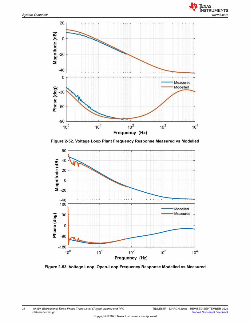
Figure 2-52. Voltage Loop Plant Frequency Response Measured vs Modelled
Figure 2-53. Voltage Loop, Open-Loop Frequency Response Modelled vs Measured
System Overview www.ti.com
38 10-kW, Bidirectional Three-Phase Three-Level (T-type) Inverter and PFC Reference Design
TIDUE53F – MARCH 2018 – REVISED SEPTEMBER 2021Submit Document Feedback
Copyright © 2021 Texas Instruments Incorporated

3 Hardware, Software, Testing Requirements, and Test Results3.1 Required Hardware and SoftwareThis section details the hardware and explains the different sections on the board and how to set them up for the experiments as outlined in this design guide.3.1.1 Hardware3.1.1.1 Test Hardware Required
The DUT in this design is set up and is operated in several pieces:
• One TIDA-01606 power board• Three TIDA-01606 gate driver cards• One TIDA-01606 ISOHVCARD• TMS320F28379D Control Card• Mini USB cable• One USB isolator• Laptop or other computer
The test equipment required to power and evaluate the design is as follows:
• 15-V, 4-A bench style supply for primary board power• For PFC Mode
– 400VL-L capable three phase AC source– > 10-kVA resistive load to be connected at the DC output
• For Inverter Mode– Star connected resistive load network like the 10-kW Simplex PowerStart load bank– 800-V, 12-A power supply for DC link input
• Four-channel, power quality analyzer• Oscilloscope, voltage meter, and current probes
The design follows an HSEC control card concept. This design can be scaled across multiple devices from the C2000™ MCU product family with a compatible HSEC control card. The key resources used for controlling the power stage on the MCU are listed in Table 3-1.
3.1.1.2 Microcontroller Resources Used on the Design
Table 3-1. Key Controller Peripherals Used for Control of Power Stage on BoardPin Number DESCRIPTION SW NAME15, 31, 28 Grid Voltage Sense Phase A, B, C TINV_VGRID_A, B, C
21, 33, 30 Inverter Side Voltage Phase A, B, C TINV_VINV_A, B, C
25, 37, 34 Inverter Side Current Phase A TINV_IINV_A, B, C
42 Bus Voltage Sensing TINV_VBUS
40 Bus Voltage Mid Point Sensing TINV_VBUS_MID
12, 14, 18, 20 Temperature A, B, C and Ambient TINV_TEMP_A, B, C, AMB
49, 50, 58 Q1 PWM Phase A, B, C TINV_Q1_A, B, C
51, 52, 60 Q3 PWM Phase A, B, C TINV_Q3_A, B, C
53, 54, 62 Q2 PWM Phase A, B, C TINV_Q2_A, B, C
99, 103, 107 SDFM Data IG A, B, C TINV_IGRID_A, B, C
101, 105, 109 SDFM Clock IG A, B, C
57, 75 SDFM Clock Source
89, 87 , 85 SiC Fault Signal A, B, C (active Low) TINV_FAULT_A, B, C
86, 88, 90, 92 Relay on A, B, C, N TINV_RELAY_A, B, C, N
61, 63 Gate driver supply PWM TINV_GATE_DRIVE
59 Control GPIO for FAN TINV_FAN
108, 110 This is used to see ISR nesting and so forth, on the docking station while starting firmware debug
TINV_PROFILING1,2
www.ti.com Hardware, Software, Testing Requirements, and Test Results
TIDUE53F – MARCH 2018 – REVISED SEPTEMBER 2021Submit Document Feedback
10-kW, Bidirectional Three-Phase Three-Level (T-type) Inverter and PFC Reference Design
39
Copyright © 2021 Texas Instruments Incorporated

Table 3-1. Key Controller Peripherals Used for Control of Power Stage on Board (continued)Pin Number DESCRIPTION SW NAME95 Gate driver enable TNV_PWM_EN
81 Gate driver Reset TINV_R
Table 3-2. Key Connectors and FunctionsCONNECTOR NAME FUNCTIONJ1, J2 DC+ and DC– terminals
J3, J4, J31, J32 Phases A, B, C and neutral terminals
J33 15-V auxiliary power supply
J34 Jumper for auxiliary power supply
J5, J13 HSEC control card connector slot
J23, J7, J17, J14, J20 Phase Agate driver card connector slot
J24, J15, J21, J9, J18 Phase B gate driver card connector slot
J25, J16, J22, J12, J19 Phase C gate driver card connector slot
Hardware changes to TIDA-01606 - REV-5
1. Changed R1, R5, and R47 to 3-mΩ current sense resistor.2. The current sense resistors along with AMC1306M05 (U1, U5, and U8) is used for current sensing in this
design. The current sense out phase A LEM sensor has a noise pick up issue and therefore is not used for current sensing and running the control loop.
3. Replaced R146, R149, R152 to 0 Ω.4. On the TIDA-01606E4-ISOHVCARD, replaced R18 to 15-k Ω and R26 to 0 Ω.
3.1.1.3 F28377D, F28379D Control-Card Settings
Certain settings on the device control card are needed to communicate over JTAG and use the isolated UART port. The settings also provide a correct ADC reference voltage. The following are the settings required on revision 1.1 of the F28379D control card.
Refer to the information sheet located inside C2000Ware at <sdk_install_path>\c2000ware\boards\controlCARDs\TMDSCNCD28379D:
1. A:SW1 on the control card must be set on both ends to ON (up) position to enable JTAG connection to the device and the UART connection for SFRA GUI. If this switch is OFF (down), one cannot use the isolated JTAG built in on the control card nor can SFRA GUI communicate to the device.
2. A:J1 is the connector for the USB cable that is used to communicate to the device from a host PC on which Code Composer Studio (CCS) runs.
3. A 3.3-V reference is desired for the control loop tuning on this design; therefore, set the appropriate jumpers to provide a 3.3-V reference externally to the on-chip ADC. For version 1.3 of the F28379D control card, this means SW3 and SW2 are moved to the end with "." that is, to the left, which puts 3.3-V VDDA as the reference for the ADC. Refer to the information sheet for more information.
3.1.2 Software
Find related software information at the following link:
3.1.2.1 Getting Started With Firmware3.1.2.1.1 Opening the CCS project
The software of this design is available inside C2000Ware_DigitalPower_SDK and is supported inside the powerSUITE framework. To open the project:
1. Install CCS (version 10.1 or above)2. Install C2000Ware DigitalPower SDK from the tool page3. Open CCS, and create a new workspace4. Inside CCS, go to View -> Resource Explorer. Under Resource Explorer, go to Software -> C2000Ware
DigitalPower SDK - <version> -> development kits and select this solution; that is, TIDA-01606/TIDA-010039, and click import project.
Hardware, Software, Testing Requirements, and Test Results www.ti.com
40 10-kW, Bidirectional Three-Phase Three-Level (T-type) Inverter and PFC Reference Design
TIDUE53F – MARCH 2018 – REVISED SEPTEMBER 2021Submit Document Feedback
Copyright © 2021 Texas Instruments Incorporated

3.1.2.1.2 Digital Power SDK Software Architecture
The general structure of the project is shown in <>. Once the project is imported, the Project Explorer will appear inside CCS.
Solution-specific and device-independent files that consist of the core algorithmic code are in "<solution>.c/h".
Board-specific and device-specific files are in "<solution>_hal.c/h". This file consists of device-specific drivers to run the solution. If the user wants to use a different modulation scheme or a different device, the user is required only to make changes to these files, besides changing the device support files in the project.
The "<solution>-main.c" file consists of the main framework of the project. This file consists of calls to the board and solution file that help in creating the system framework, along with the interrupt service routines (ISRs) and slow background tasks.
For this design, <solution> is "tinv" which is also referred to as the module name.
The powerSUITE page can be opened by clicking on the “main.syscfg” file, listed under the Project Explorer. The powerSUITE page generates the "<solution>_settings.h" file. This file is the only C based file used in the compile of the project that is generated by the powerSUITE page. The user must not modify this file manually, as the changes will be overwritten by powerSUITE each time the project is saved. "<solution>_user_settings.h" is included by the "<solution>_settings.h"and can be used to keep any settings that are outside the scope of powerSUITE tools such as #defines for ADC mapping, GPIOs etc.
The “Kit.json” and “solution.js” files are used internally by powerSUITE and also must not be modified by the user. Any changes to these files will result in the project not functioning properly.
The solution name is also used as the module name for all the variables and defines used in the solution.
Therefore, all variables and function calls are prepended by the TINV name (for example, TINV_vSecSensed_pu). This naming convention lets the user combine different solutions while avoiding naming conflicts.
3.1.2.1.3 Interrupts and Lab Structure
The project consists of two ISRs (ISR1 and ISR2) with ISR1 being the fastest and non-nestable ISR. ISR1 is reserved for the control loop and the PWM update. ISR1 is triggered by the PRIM_LEG1_PWM_BASE → EPWM_INT_TBCTR_U_CMPC event.
ISR2 is triggered by CPU Timer INT which is initiated by an overflow on CPU timer. It is used to run housekeeping functions such as doing a running average on the currents and voltage signals to remove noise and running the slew rate function for commanded references.
www.ti.com Hardware, Software, Testing Requirements, and Test Results
TIDUE53F – MARCH 2018 – REVISED SEPTEMBER 2021Submit Document Feedback
10-kW, Bidirectional Three-Phase Three-Level (T-type) Inverter and PFC Reference Design
41
Copyright © 2021 Texas Instruments Incorporated

TINV_HAL_setupDevice();
...
TINV_HAL_setupADC()
TINV_HAL_setupPWM()
«
TINV_globalVariablesInit();
TINV_HAL_setupBoardProtection();
«
TINV_HAL_setupInterrupt();
BackGround Loop
A1 -> TINV_runSFRABackGroundTasks();
B1 -> TINV_updateFaultStatus();
B2- > TINV_HAL_toggleLED();
B3 -> TINV_runRelayControl();
TINV_fanControl();
run ISR2 routines
..
TINV_readCurrentAndVoltageSignals();
TINV_HAL_updatePWM(...);
«.
tinv-main.c
run_ISR1_labX()
Clear Interrupt Flags
Restore Context
Return
run_ISR2()
Clear Interrupt Flags
Restore Context
Return
Enable Interrupt EINT
tinv.h
tinv.c
run_ISR2
return
return
Declaration of all global variables for the
solution module
Definition of all global variables for the
solution module
TINV_globalVariablesInit();ISR2
ISR1
main()
run_ISR1_labX
tinv_hal.c/h file provide the necessary drivers for the tinv.c/h, the tinv_main.c file to run
Figure 3-1. Software Flow Diagram
The software of this reference design is organized in seven labs, Table 3-3 lists the labs and how they have been tested. All the labs can be run on the C28x Main CPU or the Control Law Accelerator.
Hardware, Software, Testing Requirements, and Test Results www.ti.com
42 10-kW, Bidirectional Three-Phase Three-Level (T-type) Inverter and PFC Reference Design
TIDUE53F – MARCH 2018 – REVISED SEPTEMBER 2021Submit Document Feedback
Copyright © 2021 Texas Instruments Incorporated

Table 3-3. Overview of Labs to Test Reference DesignLAB NUMBER DESCRIPTION COMMENTS TEST ENVIRONMENT1 INV: PWM and ADC check Test the PWM driver, ISR
structure and execution rate, can be run on a control card. Unit test protection mechanisms. Test ADC mapping and reading of conversion data.
Control Card
2 INV: Open loop check PWM Check, ADC check, Protection Check, inverter mode DC bus connected and resistive star network as load
Control Card + Power Stage Hardware
3 INV: Closed Current Loop, Resistive load connected at AC
Control Card + Power Stage Hardware
4 INV: Closed Current Loop, Grid connected test inverter mode
Control Card +Emulated power stage under Hardware In-the Loop
5 PFC: Three phase AC source , Resistive load at DC, open Loop check
1. Check if the vGridRms, iGridRms, vBus meas are correct
2. Check if PLL is locked.
Control Card + Power Stage Hardware
6 PFC: Closed Current Loop, Resistive load connected at DC, three phase AC ?
Control Card + Power Stage Hardware
7 PFC: Closed Voltage loop + Current Loop , Resistive load connected at DC, three phase AC ?
Control Card + Power Stage Hardware
3.1.2.1.4 Building, Loading and Debugging the Firmware
To build the project, right-click on the project name and click Rebuild Project. The project builds successfully.
To load the project, first make sure in the Project Explorer the correct target configuration file is set as Active under targetConfigs (*.ccxml file). Then, click Run → Debug to launch a debugging session. In case of dual-CPU devices, a window may appear for the user to select the CPU on which the debug is to be performed. In this case, select CPU1. The project will then load on the device and the CCS debug view will become active. The code will halt at the start of the main routine.
To debug the system one would monitor the variables in the watch/expressions window. To populate this window with the correct variables, click View → Scripting Console to open the scripting console dialog box. On the upper right corner of this console, click on Open and then browse to the “setupdebugenv_lab<Number>.js” script file located inside the project folder. This will populate the watch window with the appropriate variables needed to debug the system. Enable Continuous Refresh button on the watch window to enable continuous update of values from the controller.
Real-time emulation is a special emulation feature that allows windows within Code Composer Studio to be updated while the MCU is running. This allows graphs and watch views to updated, but also allows the user to change values in watch or memory windows, and see the effect of these changes in the system without halting the processor. To enable real-time mode click on this button on the top bar of CCS <insert image>. A message box may appear. If so, select YES to enable debug events. This will set bit 1 (DGBM bit) of status register 1 (ST1) to a “0”. DGBM is the debug enable mask bit. When the DGBM bit is set to “0”, memory and register values can be passed to the host processor for updating the debugger windows.
In different labs, sometimes the currents and voltages measured or the control variables need to be verified by viewing the data in the graph window. For this Graph window can be used which in conjunction with a piece of code that runs on the controller can show a snapshot of how the values are being sensed by the controller. The values are logged by the datalogger typically in the slower ISRs. To import the graph into the CCS view select Tools => Graph => DualTime, and click Import and point to the graph1.GraphProp file inside the project folder. Two graphs will appear in CCS. Click Continuous Refresh on these graphs. A second set of graphs can also be added by importing the graph2.GraphProp file.
www.ti.com Hardware, Software, Testing Requirements, and Test Results
TIDUE53F – MARCH 2018 – REVISED SEPTEMBER 2021Submit Document Feedback
10-kW, Bidirectional Three-Phase Three-Level (T-type) Inverter and PFC Reference Design
43
Copyright © 2021 Texas Instruments Incorporated

CPU Loading
The main control ISR with Lab 3 and Lab 7 takes approximately 54 MIPS at 50-kHz rate when running from CPU1, that is approximately 27% of the CPU when running from 200-MHz F2837x processor. This includes the ADC drivers, abc-dq0 and dq0-abc transformation, transformation, PWM generation , two current control loops, one voltage loop, and the SFRA call.
3.1.2.2 Protection Scheme
Figure 3-2 explains the software functions used to setup the trip behavior on the design.TINV_HAL_setupCMPSS(TINV_IINVA/B/C_CMPSS_BASE)
ADC Pin
TINV_INVA/B/C
On Chip DAC
On Chip DAC
CMPSS H
CMPSS L
PWM X-Bar
Input X-BarTINV_FAULT_A/B/C
XBAR_INPUT1/2/3
TRIP4EPWM TZSEL
DCAEVT1
EPWM DCTRIPSEL &
TZDCSELDefine Trip
behavior in TZCTL
TINV_HAL_setupPWMforTrip(TINV_Q1/2_Q3/4_PHASEA/B/C_PWM_BASE)TINV_setupBoardProtection()
GPIO
+
±
+
±
Figure 3-2. Software Diagram for Trip Setup
TINV_updateFaultStaus() function is called periodically in a slow background task to updating Trip Flags and also resetting the latch if needed.
If a trip event has occurred, the PWM needs Trip flags need to be cleared separately. This part is typically handled in the ISR by calling TINV_clearPWMTrips()
Hardware, Software, Testing Requirements, and Test Results www.ti.com
44 10-kW, Bidirectional Three-Phase Three-Level (T-type) Inverter and PFC Reference Design
TIDUE53F – MARCH 2018 – REVISED SEPTEMBER 2021Submit Document Feedback
Copyright © 2021 Texas Instruments Incorporated

3.1.2.3 PWM Switching Scheme
Figure 3-3 is the PWM configuration used, only phase-A PWM modules time base is shown. Others are identical. EPWM11 is used for the SDFM sync on F28377.
RED
CMPA
FED
PWM
Sync
TINV_Q1_Q3_PHASEA_PWM_BASE
TIMEBASE
Continuous Action
Qualifier will come in
effect here
PWMxA Q1
PWMxB Q3
CMPA
ADC
SOCA
TINV_Q2_Q4_PHASEA_PWM_BASE
TIMEBASE
PWMxA Q2
PWMxB Q4
PWM
Sync
PWM sync is passed through
other PWMs and used to
sync the other PWM pulses
and also the time base for the
SDFM trigger which are
generated of a spare PWM
module
SDFM Filter
Reset
ISR1
Trig ISR1
Trig
Duty
changes
from
positive to
negative
SDFM Data
ready to be
read
EPWM11
TIMEBASE
ADC
SOCB
ADC
SOCA
ADC
SOCB
Figure 3-3. PWM Configuration
3.1.2.4 ADC Loading
To maintain synchronous operation all conversions are triggered as following:
TINV_Q1_Q3_A_PWM_BASE; that is, EPWM1 TBCTR_D_CMPB → EPWM1_SOCA (green), triggered every cycle,
TINV_Q1_Q3_A_PWM_BASE; that is, EPWM1 TBCTR_D_CMPB → EPWM1_SOCB (), triggered every 10th cycle,
TINV_Q2_Q4_A_PWM_BASE; that is, EPWM2 TBCTR_U_CMPB → EPWM2_SOCA, triggered every cycle
TINV_Q2_Q4_A_PWM_BASE; that is, EPWM2 TBCTR_D_CMPB → EPWM2_SOCB, triggered every cycle
TINV_Q1_Q3_A_PWM_BASE; that is, EPWM3 TBCTR_PERIOD → EPWM3_SOCA, triggered every cycle
www.ti.com Hardware, Software, Testing Requirements, and Test Results
TIDUE53F – MARCH 2018 – REVISED SEPTEMBER 2021Submit Document Feedback
10-kW, Bidirectional Three-Phase Three-Level (T-type) Inverter and PFC Reference Design
45
Copyright © 2021 Texas Instruments Incorporated

Table 3-4 shows the mapping with F2837xD on the TIDA-01606 hardware.
Table 3-4. ADC Loading ArchitectureADC-A ADC-B ADC-C ADC-D
SOC0 IINV-A → ADCIN-14, CMPSS4
TEMP_A → ADC-B0 IINV-B → ADC-C4, CMPSS5
IINV-C → ADC-D2, CMPSS8
SOC1 VGRID-A → ADC-A2, TEMP_B → ADC-B1 VGRID-B → ADC-C2 VGRID-C → ADC-D0
SOC2 VINV-A → ADC-A4 TEMP_A → ADC-B2 VINV-B → ADC-C3 VINV-C → ADC-D1
SOC3 VGRID-A → ADC-A2, TEMP_AMB → ADC-B3 VGRID-B → ADC-C2 VBUS → ADC-D5
SOC4 VGRID-A → ADC-A2, VGRID-B → ADC-C2 VGRID-C → ADC-D0
SOC5 VGRID-A → ADC-A2, VGRID-B → ADC-C2 VBUS → ADC-D5
SOC6 VGRID-C → ADC-D0
SOC7 VBUS → ADC-D5
SOC8 VGRID-C → ADC-D0
SOC9 VBUS → ADC-D5
Note
The ADC current reading is not used for the closed loop operation due to layout noise, instead SDFM bases sensing is employed to close the loop. Hence the grid current is used to close the current loop and the diagrams shall be interpreted accordingly for this change.
3.2 Testing and Results3.2.1 Lab 1
This lab is meant to be run on the control card and the docking station.
Set the project to Lab 1 by changing the Lab Number in the <settings.h> file, (this will be changed by powerSUITE GUI when using powerSUITE project)
#define TINV_LAB 1
All the other options can be left at default for now in the user_settings.h file
#if TINV_LAB == 1#define TINV_TEST_SETUP TINV_TEST_SETUP_RES_LOAD#define TINV_PROTECTION TINV_PROTECTION_DISABLED#define TINV_SFRA_TYPE TINV_SFRA_CURRENT#define TINV_SFRA_AMPLITUDE (float32_t)TINV_SFRA_INJECTION_AMPLITUDE_LEVEL2#define TINV_POWERFLOW_MODE TINV_INVERTER_MODE#define TINV_DC_CHECK 0#define TINV_SPLL_TYPE TINV_SPLL_SRF#endif
Hardware, Software, Testing Requirements, and Test Results www.ti.com
46 10-kW, Bidirectional Three-Phase Three-Level (T-type) Inverter and PFC Reference Design
TIDUE53F – MARCH 2018 – REVISED SEPTEMBER 2021Submit Document Feedback
Copyright © 2021 Texas Instruments Incorporated

Figure 3-4 shows the SW diagram when the code is running.
DATALOG
Graph
Window
ISR1
ISR2
TINV_dVal1
TINV_dVal2
TINV_dVal3
TINV_dVal4
DQ0_ABCTINV_vdInv_pu
TINV_vqInv_pu
TINV_vzInv_pu
a
c
b
PW
M
PWM1A/
PWM1B
PWM2A/
PWM2B
PWM3A/
PWM3B
PWM4A/
PWM4B
PWM5A/
PWM5B
PWM6A/
PWM6B
TINV_DC_CHECK==0
TINV_duty_A_pu
TINV_duty_B_pu
TINV_duty_C_pu
TINV_updatePWMDuty()
TINV_generateInternalReference
TINV_angle_r
adians
Out
RAMPGEN
X
TINV_PI*2.0
TINV_sine_A/B/C
TINV_cosine_A/B/C
Compute
Reference
Sinusoidal
and Cosine
Values
SPLL_3ph
SRF/DDSRFTINV_sine
TINV_cosine
Z-1
ABC_DQ0
_POS
ABC_DQ0
_NEG
TINV_runSPLL
TINV_angleSPLL_
radians
Compute
Reference
Sinusoidal
and Cosine
Values
TINV_duty_A/B/C_ref_pu
TINV_vdInvRef_pu
TINV_vqInvRef_pu
AD
C/
SD
FM
VBUS
TINV_vInv_A/B/C_sensed_pu
TINV_vBus_sensed_pu
IINV_ABC
VGRID_A/B/C
IGRID_A/B/C
VINV_A/B/C
TINV_readCurrentAndVoltageSignals()
TINV_vGrid_A/B/C_sensed_pu
TINV_iInv_A/B/C_sensed_pu
TINV_iGrid_A/B/C_sensed_pu
If(TINV_forceSensingConversion == 1)
Enable EPWM ADC SOC
TINV_forceSensingConversion = 0
else
Disable EPWM ADC SOC
AD
C/
SD
FM
TINV_readTempratureSignals()
TEMP_A/B/C/AMBTINV_tempA/B/C/AMB_sensed_pu
TINV_iGrid_A/B/C_sensed_Volts
TINV_iInv_A/B/C_sensed_Amps
TINV_vGrid_A/B/C_sensed_Volts
TINV_vBus_sensed_Volts
TINV_vInv_A/B/C_sensed_Volts
Convert PU Voltage
and Current Values to
Volts and AMps
If clearPWMTrip == 1
clear PWM Trip Flags
clearPWMTrip = 0
POWER_MEAS_
SINE_ANALYZER_
A/B/C
TINV_iGridRms_A/B/C_sensed_Volts
TINV_vGridRms_A/B/C_sensed_Volts
TINV_powerRms_A/B/C_Watts
Calculate Active and
Reactive Power from
the Measured Id/Iq and
Vd/Vq Values
TINV_activePower
TINV_reactivePower
AVG FILTER
AVG FILTER TINV_reactivePowerFilt
TINV_activePowerFilt
Figure 3-4. Lab1 Software Diagram
3.2.2 Testing Inverter Operation
Labs 2, 3, and 4 elaborate the steps for running the power stage in the inverter mode. Lab 2 is the inverter mode of operation in open loop, Lab 3 is the inverter mode of operation with closed current loop. Lab 4 is the grid connected inverter mode of operation and this is checked only under HIL platform and not on the hardware. The high voltage (800 VDC) is applied across terminals J1 and J2. 15-V auxiliary power supply is connected to terminal J33. Three phase star connected resistive load is connected across terminals J3, J4, and J31. J32 is the neutral terminal which is left unconnected to the load.
www.ti.com Hardware, Software, Testing Requirements, and Test Results
TIDUE53F – MARCH 2018 – REVISED SEPTEMBER 2021Submit Document Feedback
10-kW, Bidirectional Three-Phase Three-Level (T-type) Inverter and PFC Reference Design
47
Copyright © 2021 Texas Instruments Incorporated

3.2.2.1 Lab 2
In this lab the power stage is run in an open loop on the HW or HIL platform. Figure 3-5 shows lab setup of the actual hardware.
Connect voltage probe
+
+
IINV_A/B/C
VBUS
Filter
VINV_A/B/C VGRID_A/B/C
IGRID_A/B/C
J3
J4
J31
J32
J1
J2
DC Power Supply
800 V/ 10k W
Meas voltage using
multimeter
Star Connected Resistive Load Network
500 Ohm each
J33
Connect current probe
Power Flow
15 V DC, 2 Amps
Power Supply
Figure 3-5. Inverter Mode With Resistive Load lab Setup
Figure 3-6 shows the SW diagram.
DATALOG
Graph
Window
DQ0_ABC
TINV_generateInternalReference()
Out
RAMPGEN
ISR1
X
TINV_PI*2.0
Compute
Reference
Sinusoidal
and Cosine
Values
Z-1
a
c
b
PW
M
PWM1A/
PWM1B
PWM2A/
PWM2B
PWM3A/
PWM3B
PWM4A/
PWM4B
PWM5A/
PWM5B
PWM6A/
PWM6B
TINV_dVal1
TINV_dVal2
TINV_dVal3
TINV_dVal4
VBUS
TINV_vInv_A/B/C_sensed_pu
TINV_vBus_sensed_pu
IINV_ABC
VGRID_A/B/C
IGRID_A/B/C
VINV_A/B/C
TINV_readCurrentAndVoltageSignals()
TINV_vGrid_A/B/C_sensed_pu
TINV_iInv_A/B/C_sensed_pu
TINV_iGrid_A/B/C_sensed_pu
SPLL_3ph
SRF/DDSRFTINV_sine
TINV_cosine
TINV_runSPLL
Compute
Reference
Sinusoidal
and Cosine
Values
TINV_angleFixed
_radians
TINV_DC_C
HECK!=1
ABC_DQ0
_POS
ABC_DQ0
_POS
ABC_DQ0
_POS
ABC_DQ0
_POS
ABC_DQ0
_NEG
TINV_runTransformOnSensedSignals()
ABC_DQ0
_NEG
TINV_vdInv_pu
TINV_vqInv_pu
TINV_vzInv_pu
TINV_vdInvRef_pu
TINV_vqInvRef_pu
TINV_vzInvRef_pu
TINV_angle_r
adians
TINV_angleSPLL_
radians
TINV_duty_A_pu
TINV_duty_B_pu
TINV_duty_C_pu
TINV_sine_A/B/C
TINV_cosine_A/B/C
ISR2 not shown, same as Lab1, see Lab1 software diagram
If clearPWMTrip == 1
clear PWM Trip Flags
clearPWMTrip = 0
TINV_updatePWMDuty()
AD
C/
SD
FM
Figure 3-6. Lab2 Software Diagram
Refer to the hardware test set up section for actual details of the equipment used for configuring the test. Set the project to Lab 2 by changing the Lab Number in the <settings.h> file, (this will be changed by powerSUITE GUI when using powerSUITE project).
Hardware, Software, Testing Requirements, and Test Results www.ti.com
48 10-kW, Bidirectional Three-Phase Three-Level (T-type) Inverter and PFC Reference Design
TIDUE53F – MARCH 2018 – REVISED SEPTEMBER 2021Submit Document Feedback
Copyright © 2021 Texas Instruments Incorporated
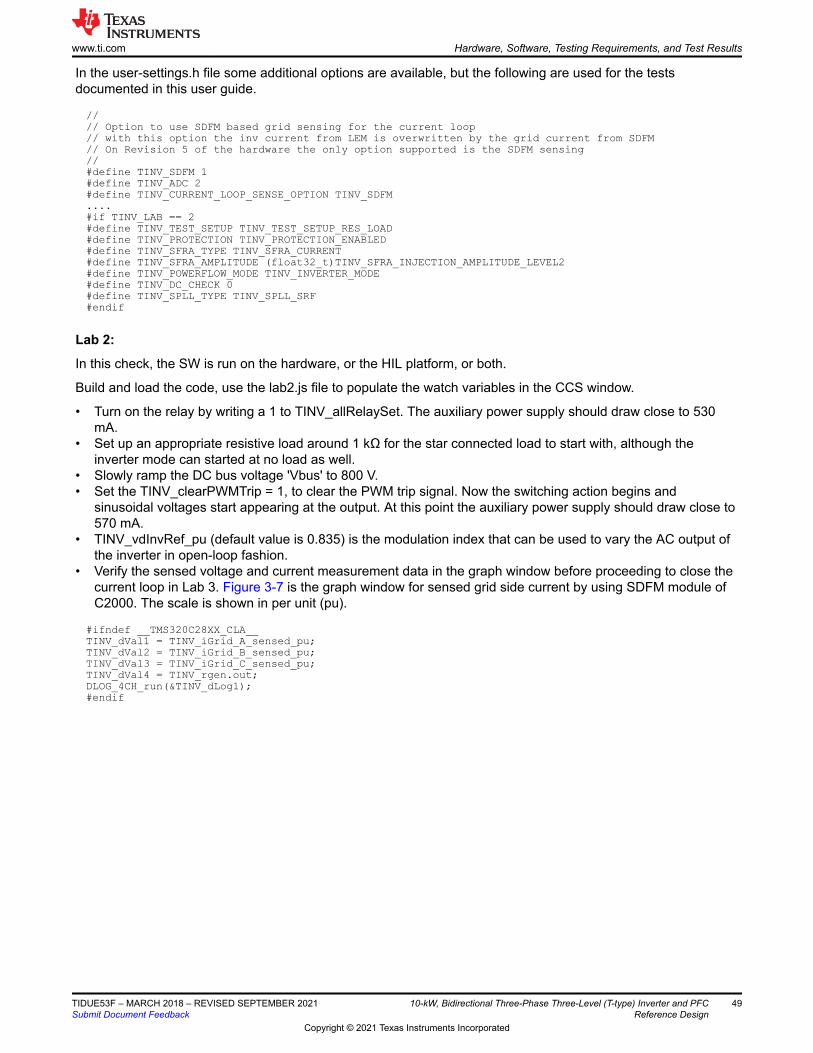
In the user-settings.h file some additional options are available, but the following are used for the tests documented in this user guide.
//// Option to use SDFM based grid sensing for the current loop// with this option the inv current from LEM is overwritten by the grid current from SDFM// On Revision 5 of the hardware the only option supported is the SDFM sensing//#define TINV_SDFM 1#define TINV_ADC 2#define TINV_CURRENT_LOOP_SENSE_OPTION TINV_SDFM....#if TINV_LAB == 2#define TINV_TEST_SETUP TINV_TEST_SETUP_RES_LOAD#define TINV_PROTECTION TINV_PROTECTION_ENABLED#define TINV_SFRA_TYPE TINV_SFRA_CURRENT#define TINV_SFRA_AMPLITUDE (float32_t)TINV_SFRA_INJECTION_AMPLITUDE_LEVEL2#define TINV_POWERFLOW_MODE TINV_INVERTER_MODE#define TINV_DC_CHECK 0#define TINV_SPLL_TYPE TINV_SPLL_SRF#endif
Lab 2:
In this check, the SW is run on the hardware, or the HIL platform, or both.
Build and load the code, use the lab2.js file to populate the watch variables in the CCS window.
• Turn on the relay by writing a 1 to TINV_allRelaySet. The auxiliary power supply should draw close to 530 mA.
• Set up an appropriate resistive load around 1 kΩ for the star connected load to start with, although the inverter mode can started at no load as well.
• Slowly ramp the DC bus voltage 'Vbus' to 800 V.• Set the TINV_clearPWMTrip = 1, to clear the PWM trip signal. Now the switching action begins and
sinusoidal voltages start appearing at the output. At this point the auxiliary power supply should draw close to 570 mA.
• TINV_vdInvRef_pu (default value is 0.835) is the modulation index that can be used to vary the AC output of the inverter in open-loop fashion.
• Verify the sensed voltage and current measurement data in the graph window before proceeding to close the current loop in Lab 3. Figure 3-7 is the graph window for sensed grid side current by using SDFM module of C2000. The scale is shown in per unit (pu).
#ifndef __TMS320C28XX_CLA__ TINV_dVal1 = TINV_iGrid_A_sensed_pu;TINV_dVal2 = TINV_iGrid_B_sensed_pu;TINV_dVal3 = TINV_iGrid_C_sensed_pu; TINV_dVal4 = TINV_rgen.out; DLOG_4CH_run(&TINV_dLog1); #endif
www.ti.com Hardware, Software, Testing Requirements, and Test Results
TIDUE53F – MARCH 2018 – REVISED SEPTEMBER 2021Submit Document Feedback
10-kW, Bidirectional Three-Phase Three-Level (T-type) Inverter and PFC Reference Design
49
Copyright © 2021 Texas Instruments Incorporated

Figure 3-7. Sensed Grid Currents
Hardware, Software, Testing Requirements, and Test Results www.ti.com
50 10-kW, Bidirectional Three-Phase Three-Level (T-type) Inverter and PFC Reference Design
TIDUE53F – MARCH 2018 – REVISED SEPTEMBER 2021Submit Document Feedback
Copyright © 2021 Texas Instruments Incorporated
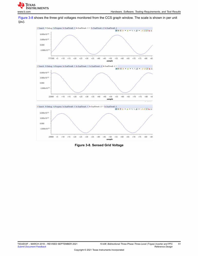
Figure 3-8 shows the three grid voltages monitored from the CCS graph window. The scale is shown in per unit (pu).
Figure 3-8. Sensed Grid Voltage
www.ti.com Hardware, Software, Testing Requirements, and Test Results
TIDUE53F – MARCH 2018 – REVISED SEPTEMBER 2021Submit Document Feedback
10-kW, Bidirectional Three-Phase Three-Level (T-type) Inverter and PFC Reference Design
51
Copyright © 2021 Texas Instruments Incorporated

Figure 3-9 shows the captured voltage and current waveform of inverter operating in open loop at 230 VAC and 1.7 kW. Scope signals: Channel 1 - DC link voltage (light green), Channel 2 - AC voltage (blue), Channel 3 - AC current (dark green).
Figure 3-9. Open Loop Inverter Voltage and Current Waveform
3.2.2.2 Lab 3
In this lab the power stage is run in an closed loop on the real HW or HIL platform. Figure 3-10 shows the SW diagram.
Hardware, Software, Testing Requirements, and Test Results www.ti.com
52 10-kW, Bidirectional Three-Phase Three-Level (T-type) Inverter and PFC Reference Design
TIDUE53F – MARCH 2018 – REVISED SEPTEMBER 2021Submit Document Feedback
Copyright © 2021 Texas Instruments Incorporated

DATALOG
Graph
Window
DQ0_ABC
TINV_generateInternalReference()
Out
RAMPGEN
ISR1
X
TINV_PI*2.0
Compute
Reference
Sinusoidal
and Cosine
Values
Z-1
a
c
b
PW
M
PWM1A/
PWM1B
PWM2A/
PWM2B
PWM3A/
PWM3B
PWM4A/
PWM4B
PWM5A/
PWM5B
PWM6A/
PWM6B
TINV_dVal1
TINV_dVal2
TINV_dVal3
TINV_dVal4
VBUS
TINV_vInv_A/B/C_sensed_pu
TINV_vBus_sensed_pu
IINV_ABC
VGRID_A/B/C
IGRID_A/B/C
VINV_A/B/C
TINV_readCurrentAndVoltageSignals()
TINV_vGrid_A/B/C_sensed_pu
TINV_iInv_A/B/C_sensed_pu
TINV_iGrid_A/B/C_sensed_pu
SPLL_3ph
SRF/DDSRFTINV_sine
TINV_cosine
TINV_runSPLL
Compute
Reference
Sinusoidal
and Cosine
Values
TINV_angleFixed
_radians
TINV_DC_C
HECK!=1
ABC_DQ0
_POS
ABC_DQ0
_POS
ABC_DQ0
_POS
ABC_DQ0
_POS
ABC_DQ0
_NEG
TINV_runTransformOnSensedSignals()
ABC_DQ0
_NEG
TINV_vdInv_pu
TINV_vqInv_pu
TINV_vzInv_pu
TINV_angle_r
adians
TINV_angleSPLL_
radians
TINV_duty_A_pu
TINV_duty_B_pu
TINV_duty_C_pu
TINV_sine_A/B/C
TINV_cosine_A/B/C
ISR2 not shown, same as Lab1, see Lab1 software diagram
TINV_updatePWMDuty()
AD
C/
SD
FM
Decoupling
network
TINV_gi_iq_out
TINV_gi_id_out
GI
Gi_id
GI
Gi_iq
TINV_iqRef_pu
TINV_idRef_pu
TINV_iGrid_dq0_pos_pu.q
TINV_iGrid_dq0_pos_pu.d
TINV_runCurrentLoop(), execute Only if
TINV_closeGiLoop==1
TINV_updatePWMDeadBand()
Figure 3-10. Lab 3 Software Diagram
Set the project to Lab 3 by changing the Lab Number in the <settings.h> file, (this will be changed by powerSUITE GUI when using powerSUITE project).
In the user settings.h file some additional options are available, but the following are used for the tests documented in this user guide.
#if TINV_LAB == 3#define TINV_TEST_SETUP TINV_TEST_SETUP_RES_LOAD#define TINV_PROTECTION TINV_PROTECTION_ENABLED#define TINV_SFRA_TYPE TINV_SFRA_CURRENT#define TINV_SFRA_AMPLITUDE (float32_t)TINV_SFRA_INJECTION_AMPLITUDE_LEVEL2#define TINV_POWERFLOW_MODE TINV_INVERTER_MODE#define TINV_DC_CHECK 0#define TINV_SPLL_TYPE TINV_SPLL_DDSRF#endif
Lab 3:
In this check, the SW is run on the hardware, or the HIL platform, or both.
Refer to the hardware test set up section for actual details of the equipment used for configuring the test. At this time, do not supply any HV power to the board.
• First launch the main.cfg and select lab3 in the project options. The compensator style (PI compensator) and the tuning loop (current loop) will be automatically populated. Now click run compensation designer icon and compensation designer tool will launch, with the model of the current loop plant with parameters specified on the powerSUITE page.
• The current compensator coefficients used for running the control loop are shown in the following code. The user can modify these coefficients to meet the necessary loop bandwidth and phase margin. The ideal coefficients with resistive load are slightly different than the one used for grid connection because the grid impedance is very low. The compensator design transfer function and response will be as shown in Figure 3-11.#define TINV_GI_PI_KP ((float32_t)0.3))#define TINV_GI_PI_KI ((float32_t)0.0120860479))
www.ti.com Hardware, Software, Testing Requirements, and Test Results
TIDUE53F – MARCH 2018 – REVISED SEPTEMBER 2021Submit Document Feedback
10-kW, Bidirectional Three-Phase Three-Level (T-type) Inverter and PFC Reference Design
53
Copyright © 2021 Texas Instruments Incorporated

• Once satisfied with the proportional and integral gain values, click on Save COMP. This will save the compensator values into the project. Close the Compensation Designer, and return to the powerSUITE page
• Build and load the code, use the lab3.js file to populate the watch variables in the CCS window.• Turn on the relay by writing a 1 to TINV_allRelaySet. The auxiliary power supply should draw close to 530
mA• Set up an appropriate resistive load around 200 Ω to start with although the inverter mode can started at no
load as well.• Slowly ramp the DC bus voltage 'Vbus' to 800 V.• Set the TINV_clearPWMTrip = 1, to clear the PWM trip signal. Now the switching action begins and
sinusoidal voltages start appearing at the output. At this point the auxiliary power supply should draw close to 570 mA.
• As soon as TINV_clearPWMTrip is set, the TINV_closeGiLoop variable is enabled and closed current loop action begins.
• TINV_idRef_pu is the current command reference and by default it is populated to a value of 0.005 pu at start-up. Slowly vary this to increase the output AC voltage and observe measured current tracks the commanded value.
• Verify TINV_idRef_pu and TINV_iInv_dq0_pos.d data in the watch window at low before proceeding to close the current loop in Lab 3.
• Slowly increase id_ref to 0.36 pu at 800-V input voltage to improve output power to 3.7 kW, approximately 1.25 kW per phase. Figure 3-11 shows the power analyzer and scope waveform.
Hardware, Software, Testing Requirements, and Test Results www.ti.com
54 10-kW, Bidirectional Three-Phase Three-Level (T-type) Inverter and PFC Reference Design
TIDUE53F – MARCH 2018 – REVISED SEPTEMBER 2021Submit Document Feedback
Copyright © 2021 Texas Instruments Incorporated

• Figure 3-11 shows the captured voltage and current waveform of inverter operating in closed current loop at 3.7 kW. Scope signals: Channel 1 - DC link voltage (blue), Channel 2 - AC voltage (light green), Channel 3 - AC current (dark green)
Figure 3-11. Inverter Closed-Loop Operation
• SFRA is integrated in the software of this lab to verify the designed compensator provides enough gain and phase margin by measuring on hardware. To run the SFRA keep the project running, and from the cfg page, click on the SFRA icon. SFRA GUI will pop up.
• Select the options for the device on the SFRA GUI. For example, for F28377D select floating point. Click on Setup Connection. On the pop-up window uncheck the boot on connect option, and select an appropriate COM port. Click OK. Return to the SFRA GUI, and click Connect.
• The SFRA GUI will connect to the device. A SFRA sweep can now be started by clicking Start Sweep. The complete SFRA sweep will take a few minutes to finish. Activity can be monitored by seeing the progress bar on the SFRA GUI and also checking the flashing of blue LED on the back on the control card that indicates UART activity. Once complete, a graph with the open loop plot will appear, as in Figure 3-12. This verifies that the designed compensator is indeed stable. The SFRA for plant and open loop with the above coefficients is shown in Figure 3-12 and Figure 3-13, respectively. This action verifies the current compensator design. To bring the system to a safe stop, bring the input DC voltage down to zero.
• The above set of compensation designer coefficients are robust and stable. In case the tracking performance of current against the commanded reference and appears to oscillate, the user can use the following set of coefficients. To change the coefficients, compensation designer tool will have to be relaunched from the power suite page.#define TINV_GI_PI_KP ((float32_t)0.144))#define TINV_GI_PI_KI ((float32_t)0.112))
• Once satisfied with the proportional and integral gain values, click on Save COMP. This will save the compensator values into the project.
www.ti.com Hardware, Software, Testing Requirements, and Test Results
TIDUE53F – MARCH 2018 – REVISED SEPTEMBER 2021Submit Document Feedback
10-kW, Bidirectional Three-Phase Three-Level (T-type) Inverter and PFC Reference Design
55
Copyright © 2021 Texas Instruments Incorporated

• The SFRA response of plant and open loop for the inverter in current mode with the new set of coefficients are shown in Figure 3-12 and Figure 3-13, respectively.
Figure 3-12. Inverter SFRA Plant Response for Current Loop
Figure 3-13. Inverter SFRA Loop Response for Current Loop
Hardware, Software, Testing Requirements, and Test Results www.ti.com
56 10-kW, Bidirectional Three-Phase Three-Level (T-type) Inverter and PFC Reference Design
TIDUE53F – MARCH 2018 – REVISED SEPTEMBER 2021Submit Document Feedback
Copyright © 2021 Texas Instruments Incorporated
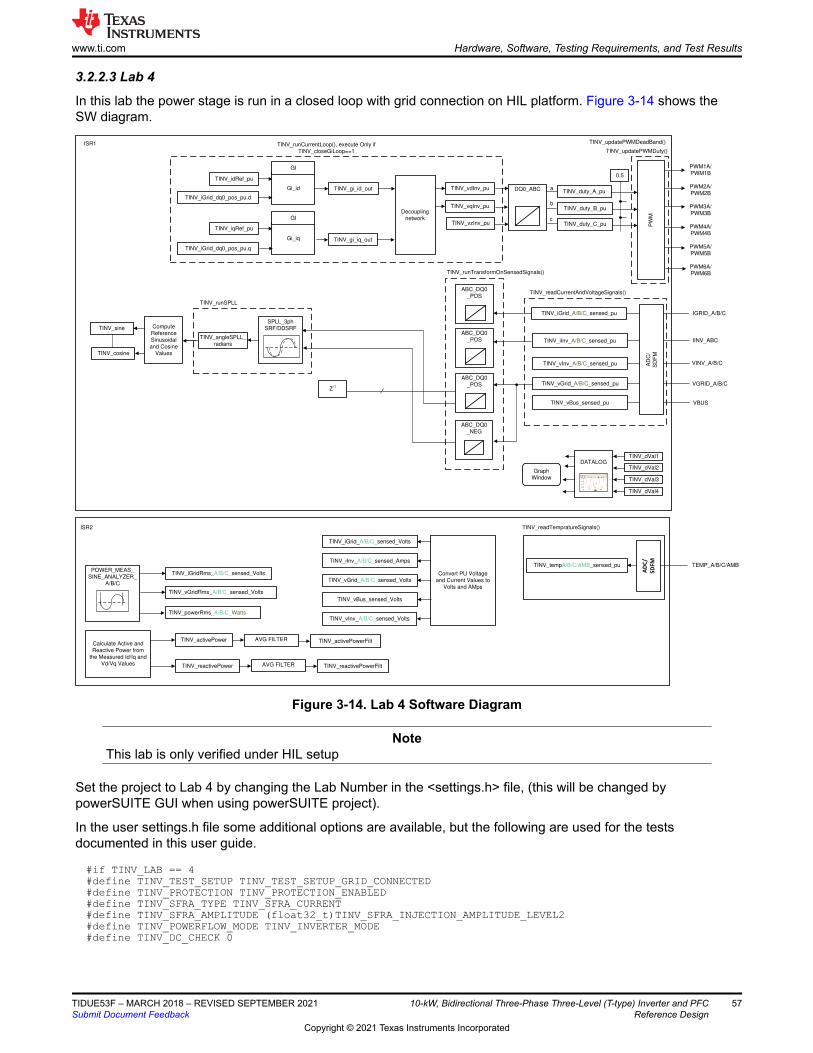
3.2.2.3 Lab 4
In this lab the power stage is run in a closed loop with grid connection on HIL platform. Figure 3-14 shows the SW diagram.
DATALOG
Graph
Window
DQ0_ABC
ISR1
Z-1
a
c
b
PW
M
PWM1A/
PWM1B
PWM2A/
PWM2B
PWM3A/
PWM3B
PWM4A/
PWM4B
PWM5A/
PWM5B
PWM6A/
PWM6B
TINV_dVal1
TINV_dVal2
TINV_dVal3
TINV_dVal4
VBUS
TINV_vInv_A/B/C_sensed_pu
TINV_vBus_sensed_pu
IINV_ABC
VGRID_A/B/C
IGRID_A/B/C
VINV_A/B/C
TINV_readCurrentAndVoltageSignals()
TINV_vGrid_A/B/C_sensed_pu
TINV_iInv_A/B/C_sensed_pu
TINV_iGrid_A/B/C_sensed_pu
SPLL_3ph
SRF/DDSRFTINV_sine
TINV_cosine
TINV_runSPLL
Compute
Reference
Sinusoidal
and Cosine
Values
ABC_DQ0
_POS
ABC_DQ0
_POS
ABC_DQ0
_POS
TINV_runTransformOnSensedSignals()
ABC_DQ0
_NEG
TINV_vdInv_pu
TINV_vqInv_pu
TINV_vzInv_pu
TINV_angleSPLL_
radians
TINV_duty_A_pu
TINV_duty_B_pu
TINV_duty_C_pu
TINV_updatePWMDuty()
AD
C/
SD
FM
Decoupling
network
TINV_gi_iq_out
TINV_gi_id_out
GI
Gi_id
GI
Gi_iq
TINV_iqRef_pu
TINV_idRef_pu
TINV_iGrid_dq0_pos_pu.q
TINV_iGrid_dq0_pos_pu.d
TINV_runCurrentLoop(), execute Only if
TINV_closeGiLoop==1
TINV_updatePWMDeadBand()
AD
C/
SD
FM
TINV_readTempratureSignals()
TEMP_A/B/C/AMBTINV_tempA/B/C/AMB_sensed_pu
TINV_iGrid_A/B/C_sensed_Volts
TINV_iInv_A/B/C_sensed_Amps
TINV_vGrid_A/B/C_sensed_Volts
TINV_vBus_sensed_Volts
TINV_vInv_A/B/C_sensed_Volts
Convert PU Voltage
and Current Values to
Volts and AMps
POWER_MEAS_
SINE_ANALYZER_
A/B/C
TINV_iGridRms_A/B/C_sensed_Volts
TINV_vGridRms_A/B/C_sensed_Volts
TINV_powerRms_A/B/C_Watts
Calculate Active and
Reactive Power from
the Measured Id/Iq and
Vd/Vq Values
TINV_activePower
TINV_reactivePower
AVG FILTER
AVG FILTER TINV_reactivePowerFilt
TINV_activePowerFilt
ISR2
AD
C/
SD
FM
0.5
Figure 3-14. Lab 4 Software Diagram
NoteThis lab is only verified under HIL setup
Set the project to Lab 4 by changing the Lab Number in the <settings.h> file, (this will be changed by powerSUITE GUI when using powerSUITE project).
In the user settings.h file some additional options are available, but the following are used for the tests documented in this user guide.
#if TINV_LAB == 4#define TINV_TEST_SETUP TINV_TEST_SETUP_GRID_CONNECTED#define TINV_PROTECTION TINV_PROTECTION_ENABLED#define TINV_SFRA_TYPE TINV_SFRA_CURRENT#define TINV_SFRA_AMPLITUDE (float32_t)TINV_SFRA_INJECTION_AMPLITUDE_LEVEL2#define TINV_POWERFLOW_MODE TINV_INVERTER_MODE#define TINV_DC_CHECK 0
www.ti.com Hardware, Software, Testing Requirements, and Test Results
TIDUE53F – MARCH 2018 – REVISED SEPTEMBER 2021Submit Document Feedback
10-kW, Bidirectional Three-Phase Three-Level (T-type) Inverter and PFC Reference Design
57
Copyright © 2021 Texas Instruments Incorporated

#define TINV_SPLL_TYPE TINV_SPLL_SRF#endif
Lab 4
In this check, the SW is run on the HIL platform.
Build and load the code, use the lab4.js file to populate the watch variables in the CCS window.
• Slowly ramp the DC bus voltage 'Vbus' to 800 V• Enter "1" on TINV_startPowerStage variable and ramp the AC voltage of the grid to 230Vrms, L-N; that is,
400 VL-L• Set up an appropriate grid connection and turn on the relay by writing a 1 to TINV_allRelaySet as soon as
voltage reaches 230 VRMS as the inrush current limit resistors might get heated and burn out. The current should now be fed into the grid.
• Slowly increase this TINV_idRef_pu variable to be 0.6 pu, at this point the per phase power will be approximately 1.9 kW
Measure the current loop bandwidth using SFRA. Figure 3-15 and Figure 3-16 show plant response and loop response of inverter operating in current mode measured on the HIL platform.
Figure 3-15. Inverter SFRA Plant Response Measured on HIL
Hardware, Software, Testing Requirements, and Test Results www.ti.com
58 10-kW, Bidirectional Three-Phase Three-Level (T-type) Inverter and PFC Reference Design
TIDUE53F – MARCH 2018 – REVISED SEPTEMBER 2021Submit Document Feedback
Copyright © 2021 Texas Instruments Incorporated

Figure 3-16. Inverter SFRA Loop Response Measured on HIL
3.2.3 Testing PFC Operation
Labs 5, 6, and 7 elaborate the steps for running the power stage in the PFC mode. Lab 5 is the PFC mode of operation in open loop, Lab 6 is the PFC mode of operation with closed current loop. Lab 7 is the PFC mode of operation in closed voltage and current loop and this will be checked both on the HIL platform and actual hardware. Figure 3-17 shows the hardware setup, the DC terminals J1 and J2 are connected to a resistive load. 15-V auxiliary power supply is connected to terminal J33. Three phase AC source is connected across terminals J3, J4, and J31 (A, B, and C). J32 is the neutral terminal which is left unconnected to the source. See the hardware test set up section for actual details of the equipment used for configuring the test.
Connect voltage probe
+
+
IINV_A/B/C
VBUS
Filter
VINV_A/B/C VGRID_A/B/C
IGRID_A/B/C
J3
J4
J31
J32
J1
J2
Load
(640 Ohms Power
Resistors)
Meas voltage using
multimeter
J33
Connect current probe
Power Flow
15 V DC, 2 Amps
Power Supply
AC Power Source
Three Phase
230 Vrms L-N
50 Hz
Figure 3-17. PFC Mode Test Setup
www.ti.com Hardware, Software, Testing Requirements, and Test Results
TIDUE53F – MARCH 2018 – REVISED SEPTEMBER 2021Submit Document Feedback
10-kW, Bidirectional Three-Phase Three-Level (T-type) Inverter and PFC Reference Design
59
Copyright © 2021 Texas Instruments Incorporated

3.2.3.1 Lab 5
This is the first PFC lab. In this lab sensing is checked and no switching action occurs until clearPWMTrip is set to 1.
The hardware setup for the PFC mode is explained in Figure 3-17. TI recommends starting the PFC at low voltage like 30 VRMS and connecting a 2-kΩ resistor.
Set the project to Lab 5 by changing the Lab Number in the <settings.h> file, (this will be changed by powerSUITE GUI when using powerSUITE project).
Under this condition, the converter operates as a rectifier and rectified current can be observed being drawn without any power factor correction. SPLL locking can also be safely verified in this build.
DATALOG
Graph
Window
DQ0_ABC
ISR1
Z-1
a
c
b
PW
M
PWM1A/
PWM1B
PWM2A/
PWM2B
PWM3A/
PWM3B
PWM4A/
PWM4B
PWM5A/
PWM5B
PWM6A/
PWM6B
TINV_dVal1
TINV_dVal2
TINV_dVal3
TINV_dVal4
VBUS
TINV_vInv_A/B/C_sensed_pu
TINV_vBus_sensed_pu
IINV_ABC
VGRID_A/B/C
IGRID_A/B/C
VINV_A/B/C
TINV_readCurrentAndVoltageSignals()
TINV_vGrid_A/B/C_sensed_pu
TINV_iInv_A/B/C_sensed_pu
TINV_iGrid_A/B/C_sensed_pu
SPLL_3ph
SRF/DDSRFTINV_sine
TINV_cosine
TINV_runSPLL
Compute
Reference
Sinusoidal
and Cosine
Values
ABC_DQ0
_POS
ABC_DQ0
_POS
ABC_DQ0
_POS
TINV_runTransformOnSensedSignals()
ABC_DQ0
_NEG
TINV_angleSPLL_
radians
TINV_duty_A_pu
TINV_duty_B_pu
TINV_duty_C_pu
TINV_updatePWMDuty()
AD
C/
SD
FM
AD
C/
SD
FM
TINV_readTempratureSignals()
TEMP_A/B/C/AMBTINV_tempA/B/C/AMB_sensed_pu
TINV_iGrid_A/B/C_sensed_Volts
TINV_iInv_A/B/C_sensed_Amps
TINV_vGrid_A/B/C_sensed_Volts
TINV_vBus_sensed_Volts
TINV_vInv_A/B/C_sensed_Volts
Convert PU Voltage
and Current Values to
Volts and AMps
POWER_MEAS_
SINE_ANALYZER_
A/B/C
TINV_iGridRms_A/B/C_sensed_Volts
TINV_vGridRms_A/B/C_sensed_Volts
TINV_powerRms_A/B/C_Watts
Calculate Active and
Reactive Power from
the Measured Id/Iq and
Vd/Vq Values
TINV_activePower
TINV_reactivePower
AVG FILTER
AVG FILTER TINV_reactivePowerFilt
TINV_activePowerFilt
ISR2A
DC
/
SD
FM
If clearPWMTrip == 1
clear PWM Trip Flags
clearPWMTrip = 0
TINV_vdInv_pu
TINV_vqInv_pu
TINV_vzInv_pu
TINV_vdInvRef_pu
TINV_vqInvRef_pu
TINV_vzInvRef_pu
Figure 3-18. Lab 5 Software Diagram
Hence, the following variables are put on the datalogger:
TINV_dVal1 = TINV_vGrid_A_sensed_pu;TINV_dVal2 = TINV_angleSPLL_radians / (float32_t)(2.0f * TINV_PI);TINV_dVal3 = TINV_vGrid_A_sensed_pu;TINV_dVal4 = TINV_iInv_A_sensed_pu;DLOG_4CH_run(&TINV_dLog1);
Hardware, Software, Testing Requirements, and Test Results www.ti.com
60 10-kW, Bidirectional Three-Phase Three-Level (T-type) Inverter and PFC Reference Design
TIDUE53F – MARCH 2018 – REVISED SEPTEMBER 2021Submit Document Feedback
Copyright © 2021 Texas Instruments Incorporated

Make sure the Grid frequency is specified correctly, the grid frequency can be changed through the sysconfig page for powerSUITE based projects. If not powerSUITE based project one can modify the tinv_settings.h file.
#define TINV_AC_FREQ_HZ ((float32_t)50)
Build and load the code, use the lab5.js file to populate the watch variables in the CCS window.
PLL lock can be checked by plotting the buffers, use the graph1.graphprop to see the buffer through Tools→ Graph → Dual Time.
Cosine transforms are used hence the angle will be 0 when the Vgrid as its peak.
First close the relay by writing a 1 to TINV_allRelaySet
Initially, the test may be run with only 30 VRMS for safety, hence safely ramp the AC supply to 30 VRMS and observe the graph in the CCS debug window to confirm the PLL is locking. Figure 3-19 shows low voltage phase locked loop check from watch window.
Figure 3-19. PLL - Grid Voltage Synchronization
If the PLL is not locking one may also issue a tinv_reset_PLL command by setting it to 1, this will initiate a task to zero out an integrated error in the module and zero all the memory elements.
Similarly, the current flowing from the grid across all phases can be checked, using the graph watch window of CCS. Figure 3-20 shows the Sensed grid currents from graph windowCheck for three phase grid currents observed from the watch window.
Figure 3-20. Sensed Grid Currents - PFC Mode
www.ti.com Hardware, Software, Testing Requirements, and Test Results
TIDUE53F – MARCH 2018 – REVISED SEPTEMBER 2021Submit Document Feedback
10-kW, Bidirectional Three-Phase Three-Level (T-type) Inverter and PFC Reference Design
61
Copyright © 2021 Texas Instruments Incorporated

To verify boost action in Lab 5, follow the steps according to the sequence provided:
• Turn on the auxiliary power supply and set it to 15 V and then debug and run the code.• Connect suitable load to the terminals J1 and J2. Make sure to use a high load resistance (around 2 kΩ)
which otherwise can lead to high inrush currents triggering the overcurrent flag.• Apply 30 VRMS AC voltage to the three phase terminals• Immediately turn on the relay by writing a 1 to TINV_allRelaySet. Voltage should now start to appear across
the DC terminals.• Clear the PWM trip by setting TINV_clearPwmTrip to 1 to see a slight boost in DC voltage.
Before PFC action begins, a rectified current will be drawn due to the load on the Vbus. As soon as clearPWMTrip is set to 1, a slight boost in DC voltage is seen. Note the input current has a double bump without the neutral connected to the source at light load.
Note
There can be a situation in the labs for PFC (Lab 5, Lab 6, and Lab 7) where the converter operates as a rectifier and rectified current is seen being drawn without any power factor correction. But as soon as TINV_clearPwmTrip is set to 1, there is no switching action – the Gate Signals remain off.
This is because there is an overcurrent or DSAT flag (InvA_overcurrent, InvB_overcurrent,DSATA, DSATB) which is set in one of the three phases and this happens under three circumstances:1. On closing the relays, there is an inrush current which creates an overcurrent trip in one of the
three phases.2. When TINV_clearPwmTrip to 1, the switching action causes one of the flags to be set.3. Setting TINV_StartpowerStage to 1 for closing the current and voltage loop.
The EPWM TZFLG is set to 0X000C and under this condition no switching occurs. So make sure the load resistance is increased so that the inrush currents will not cause a trip condition and the EPWM TZFLG changes from 0x0004 to 0x0000 and switching occurs.
Once the FLG is set to 0x000C, even if we do a TINV_reset_fault_status to reset the faults, though the faults may be cleared PWM action will not be observed.
The goal is, as soon as the auxiliary power supply is started and the code debugged, all the faults – namely InvA_overcurrent, InvB_overcurrent, DSATA, DSATB; and so forth – should be set to zero so that the controller does not go into a trip state.
3.2.3.2 Lab 6
In this build level the current loop for the PFC is checked. Lab 6 is primarily meant for tuning the current loop and optimizing its performance. It is always safe to start Lab 6 at low voltage and low power as starting at higher power without a supervisory voltage loop can boost the voltage due to overcurrent events and can blow away the switches. Hence, it is very important to carefully set the TINV_idRef_pu variable so as to avoid overcurrent trips and high voltages at the DC terminals. Also the TINV_idRef_pu is defined with a negative sign for PFC mode of operation and with a positive sign for inverter mode of operation.
Figure 3-21 describes the software flow for running Lab 6.
Hardware, Software, Testing Requirements, and Test Results www.ti.com
62 10-kW, Bidirectional Three-Phase Three-Level (T-type) Inverter and PFC Reference Design
TIDUE53F – MARCH 2018 – REVISED SEPTEMBER 2021Submit Document Feedback
Copyright © 2021 Texas Instruments Incorporated

DATALOG
Graph
Window
DQ0_ABC
ISR1
Z-1
a
c
b
PW
M
PWM1A/
PWM1B
PWM2A/
PWM2B
PWM3A/
PWM3B
PWM4A/
PWM4B
PWM5A/
PWM5B
PWM6A/
PWM6B
TINV_dVal1
TINV_dVal2
TINV_dVal3
TINV_dVal4
VBUS
TINV_vInv_A/B/C_sensed_pu
TINV_vBus_sensed_pu
IINV_ABC
VGRID_A/B/C
IGRID_A/B/C
VINV_A/B/C
TINV_readCurrentAndVoltageSignals()
TINV_vGrid_A/B/C_sensed_pu
TINV_iInv_A/B/C_sensed_pu
TINV_iGrid_A/B/C_sensed_pu
SPLL_3ph
SRF/DDSRFTINV_sine
TINV_cosine
TINV_runSPLL
Compute
Reference
Sinusoidal
and Cosine
Values
ABC_DQ0
_POS
ABC_DQ0
_POS
ABC_DQ0
_POS
TINV_runTransformOnSensedSignals()
ABC_DQ0
_NEG
TINV_vdInv_pu
TINV_vqInv_pu
TINV_vzInv_pu
TINV_angleSPLL_
radians
TINV_duty_A_pu
TINV_duty_B_pu
TINV_duty_C_pu
TINV_updatePWMDuty()
AD
C/
SD
FM
Decoupling
network
TINV_gi_iq_out
TINV_gi_id_out
GI
Gi_id
GI
Gi_iq
TINV_iqRef_pu
TINV_idRef_pu
TINV_iGrid_dq0_pos_pu.q
TINV_iGrid_dq0_pos_pu.d
TINV_runCurrentLoop(), execute Only if
TINV_closeGiLoop==1
TINV_updatePWMDeadBand()
AD
C/
SD
FM
TINV_readTempratureSignals()
TEMP_A/B/C/AMBTINV_tempA/B/C/AMB_sensed_pu
TINV_iGrid_A/B/C_sensed_Volts
TINV_iInv_A/B/C_sensed_Amps
TINV_vGrid_A/B/C_sensed_Volts
TINV_vBus_sensed_Volts
TINV_vInv_A/B/C_sensed_Volts
Convert PU Voltage
and Current Values to
Volts and AMps
POWER_MEAS_
SINE_ANALYZER_
A/B/C
TINV_iGridRms_A/B/C_sensed_Volts
TINV_vGridRms_A/B/C_sensed_Volts
TINV_powerRms_A/B/C_Watts
Calculate Active and
Reactive Power from
the Measured Id/Iq and
Vd/Vq Values
TINV_activePower
TINV_reactivePower
AVG FILTER
AVG FILTER TINV_reactivePowerFilt
TINV_activePowerFilt
ISR2
AD
C/
SD
FM
0.5
If startPowerStage == 1
Wait for PhaseA Zero Crossing to
clear PWM Trips and set closeGiLoop to 1
TINV_closeGiLoop==1
TINV_deadBandMax
Slew Deadband for
soft start of duty
Figure 3-21. Lab 6 Software Diagram
Set the project to Lab 6 by changing the Lab Number in the <settings.h> file, (this will be changed by powerSUITE GUI when using powerSUITE project)
In the user settings.h file some additional options are available, but the following are used for the tests documented in this user guide.
#if TINV_LAB == 6#define TINV_TEST_SETUP TINV_TEST_SETUP_RES_LOAD#define TINV_PROTECTION TINV_PROTECTION_ENABLED#define TINV_SFRA_TYPE TINV_SFRA_CURRENT#define TINV_SFRA_AMPLITUDE (float32_t)TINV_SFRA_INJECTION_AMPLITUDE_LEVEL2#define TINV_POWERFLOW_MODE TINV_RECTIFIERER_MODE#define TINV_DC_CHECK 0#define TINV_SPLL_TYPE TINV_SPLL_SRF#endif
In this check the SW is run on the hardware, or the HIL platform, or both.
Refer to the hardware test set up section for actual details of the equipment used for configuring the test. Do not supply any HV power yet to the board.
• First launch the main.cfg and select Lab 6 in the project options. The compensator style (PI compensator) and the tuning loop (current loop) will be automatically populated. Now click run compensation designer
www.ti.com Hardware, Software, Testing Requirements, and Test Results
TIDUE53F – MARCH 2018 – REVISED SEPTEMBER 2021Submit Document Feedback
10-kW, Bidirectional Three-Phase Three-Level (T-type) Inverter and PFC Reference Design
63
Copyright © 2021 Texas Instruments Incorporated

icon and compensation designer tool will launch, with the model of the current loop plant with parameters specified on the powerSUITE page.
• The current compensator coefficients used for running the control loop are shown in the following code. The user can modify these coefficients to meet the necessary loop bandwidth and phase margin. The ideal coefficients with resistive load are slightly different than the one used for grid connection because the grid impedance is very low. The compensator design transfer function and response are shown in Figure 3-22.#define TINV_GI_PI_KP ((float32_t)0.3))#define TINV_GI_PI_KI ((float32_t)0.0120860479))
Figure 3-22. Compensator Design GUI - Current Loop PI Coefficients• Once satisfied with the proportional and integral gain values, click on Save COMP. This will save the
compensator values into the project. Close the Compensation Designer, and return to the powerSUITE page.• Turn on the auxiliary power supply and set it to 15 V. Build and load the code, use the lab6.js file to populate
the watch variables in the CCS window.• Set the load resistance to a high value 3.18 kΩ.• Set the AC input voltage to 30 VRMS with appropriate current limit.• After turning on the AC power supply, immediately turn on the relay by writing a 1 to TINV_allRelaySet.
Ensure that the relay is turned on immediately (within 3-4 seconds) after turning on the ac supply.• Set TINV_idRef_pu to –0.013 pu• To start the PFC mode, enter "1" on TINV_startPowerStage variable, the current should now be drawn from
the grid as a sinusoidal signal (with some harmonics as it is at low power) and boost action seen on the vBus. The output voltage will boost from 75 V to around 180 V as shown in Figure 3-23.
• The current will become sinusoidal as the load is increased. This verifies start up of PFC at 30 VRMS.• The Figure 3-23 shows PFC closed current loop start up at 30 VRMS. Scope signals: Channel 1 - AC voltage
(blue), Channel 2- DC voltage (light green), Channel 3 - AC current (dark green).
Hardware, Software, Testing Requirements, and Test Results www.ti.com
64 10-kW, Bidirectional Three-Phase Three-Level (T-type) Inverter and PFC Reference Design
TIDUE53F – MARCH 2018 – REVISED SEPTEMBER 2021Submit Document Feedback
Copyright © 2021 Texas Instruments Incorporated

Figure 3-23. PFC Current Loop Start-up at 30 VRMS • Now repeat the previous steps to verify start up at 220 VRMS.
At 220 VRMS, with the TINV_idRef_pu set to –0.013 pu, the bus voltage jumps from 550 V to 640 V at 155 W power as Figure 3-24 shows.
• Figure 3-24 shows PFC closed current loop start up at 220 VRMS. Scope signals: Channel 1 - AC voltage (blue), Channel 2 - DC voltage (light green), Channel 3 - AC current (dark green)
Figure 3-24. PFC Current Loop Start-up at 220 VRMS • As Figure 3-24 shows, running this lab at higher input voltage without a supervisory voltage loop results in
big overvoltage across the DC terminals. Hence it is always advisable to start this lab at low voltage and low power as previously described for safety reasons and then slowly ramp to the desired voltage for closed
www.ti.com Hardware, Software, Testing Requirements, and Test Results
TIDUE53F – MARCH 2018 – REVISED SEPTEMBER 2021Submit Document Feedback
10-kW, Bidirectional Three-Phase Three-Level (T-type) Inverter and PFC Reference Design
65
Copyright © 2021 Texas Instruments Incorporated

current loop tuning. Starting at 230-VRMS AC input voltage and boosting DC voltage to 800 V directly is shown in Lab 7.
• In case any overcurrent trip is observed which causes the PWMs to switch off, please refer the notes in Lab 5 to debug this condition.
• A soft start scheme is implemented at the start-up to ensure overcurrents are reduced at start-up. For this the duty is restricted to the PWM module by adjusting the dead band set Figure 3-25 shows the PWM configuration for this setup where the dead band is set to large value and slowly reduced to the nominal value to limit the current spikes.
TYPICAL_RED
CMPA
TYPICAL_FED
TINV_Q1_Q3_PHASEA_PWM_BASE
TIMEBASE
PWMxA Q1
PWMxB Q3
RED_SOFT_START
FED_SOFT_START
Figure 3-25. Dead Band Soft Start PWM Configuration
• Figure 3-26 shows the effect of the start-up scheme without dead band implemented at start-up. Without soft start, a huge current spike appears which causes over current trip and the DC bus voltage also collapses. Figure 3-26 shows overcurrent without soft-start implementation. Channel 1 - AC voltage (blue), Channel 2 - AC current (light green), Channel 3 - DC voltage (dark green)
Figure 3-26. Without Soft Start
Hardware, Software, Testing Requirements, and Test Results www.ti.com
66 10-kW, Bidirectional Three-Phase Three-Level (T-type) Inverter and PFC Reference Design
TIDUE53F – MARCH 2018 – REVISED SEPTEMBER 2021Submit Document Feedback
Copyright © 2021 Texas Instruments Incorporated

Figure 3-27 shows reduced current spike with soft-start implementation. Channel 1 - AC voltage (blue), Channel 2 - AC current (light green), Channel 3 - DC voltage (dark green).
Figure 3-27. Soft Start With Adaptive Dead Band
• SFRA is integrated in the software of this lab to verify the designed compensator provides enough gain and phase margin by measuring on hardware. To run the SFRA keep the project running, and from the cfg page, click on the SFRA icon. SFRA GUI will pop up.
• Select the options for the device on the SFRA GUI. For example, for F28377D select floating point. Click on Setup Connection. On the pop-up window uncheck the boot on connect option, and select an appropriate COM port. Click OK. Return to the SFRA GUI, and click Connect.
• The SFRA GUI will connect to the device. A SFRA sweep can now be started by clicking Start Sweep. The complete SFRA sweep will take a few minutes to finish. Activity can be monitored by seeing the progress bar on the SFRA GUI and also checking the flashing of blue LED on the back on the control card that indicates UART activity. Once complete, a graph with the open loop plot will appear, as in Figure 3-28 and Figure 3-29 which corresponds to plant and loop response measured by SFRA GUI respectively. This verifies that the designed compensator is indeed stable
www.ti.com Hardware, Software, Testing Requirements, and Test Results
TIDUE53F – MARCH 2018 – REVISED SEPTEMBER 2021Submit Document Feedback
10-kW, Bidirectional Three-Phase Three-Level (T-type) Inverter and PFC Reference Design
67
Copyright © 2021 Texas Instruments Incorporated

Figure 3-28. PFC SFRA Plant Response for Current Loop
Figure 3-29. PFC SFRA Loop Response for Current Loop• The frequency response data is also saved in the project folder under an SFRA data folder and is time
stamped with the time of the SFRA run.• This completes verification of Lab 6.
Hardware, Software, Testing Requirements, and Test Results www.ti.com
68 10-kW, Bidirectional Three-Phase Three-Level (T-type) Inverter and PFC Reference Design
TIDUE53F – MARCH 2018 – REVISED SEPTEMBER 2021Submit Document Feedback
Copyright © 2021 Texas Instruments Incorporated

3.2.3.3 Lab 7
In this build level the voltage and current loop for the PFC is checked. Here the variable TINV_vBusRef_pu is defined to set the voltage at which the output DC bus voltage is to be regulated.
Figure 3-30 describes the software flow for running Lab 7.
DATALOG
Graph
Window
DQ0_ABC
ISR1
Z-1
a
c
b
PW
M
PWM1A/
PWM1B
PWM2A/
PWM2B
PWM3A/
PWM3B
PWM4A/
PWM4B
PWM5A/
PWM5B
PWM6A/
PWM6B
TINV_dVal1
TINV_dVal2
TINV_dVal3
TINV_dVal4
VBUS
TINV_vInv_A/B/C_sensed_pu
TINV_vBus_sensed_pu
IINV_ABC
VGRID_A/B/C
IGRID_A/B/C
VINV_A/B/C
TINV_readCurrentAndVoltageSignals()
TINV_vGrid_A/B/C_sensed_pu
TINV_iInv_A/B/C_sensed_pu
TINV_iGrid_A/B/C_sensed_pu
SPLL_3ph
SRF/DDSRFTINV_sine
TINV_cosine
TINV_runSPLL
Compute
Reference
Sinusoidal
and Cosine
Values
ABC_DQ0
_POS
ABC_DQ0
_POS
ABC_DQ0
_POS
TINV_runTransformOnSensedSignals()
ABC_DQ0
_NEG
TINV_vdInv_pu
TINV_vqInv_pu
TINV_vzInv_pu
TINV_angleSPLL_
radians
TINV_duty_A_pu
TINV_duty_B_pu
TINV_duty_C_pu
TINV_updatePWMDuty()
AD
C/
SD
FM
Decoupling
network
TINV_gi_iq_out
TINV_gi_id_out
GI
Gi_id
GI
Gi_iq
TINV_iqRef_pu
TINV_idRef_pu
TINV_iGrid_dq0_pos_pu.q
TINV_iGrid_dq0_pos_pu.d
TINV_runCurrentLoop(), execute Only if
TINV_closeGiLoop==1
TINV_updatePWMDeadBand()
AD
C/
SD
FM
TINV_readTempratureSignals()
TEMP_A/B/C/AMBTINV_tempA/B/C/AMB_sensed_pu
TINV_iGrid_A/B/C_sensed_Volts
TINV_iInv_A/B/C_sensed_Amps
TINV_vGrid_A/B/C_sensed_Volts
TINV_vBus_sensed_Volts
TINV_vInv_A/B/C_sensed_Volts
Convert PU Voltage
and Current Values to
Volts and AMps
POWER_MEAS_
SINE_ANALYZER_
A/B/C
TINV_iGridRms_A/B/C_sensed_Volts
TINV_vGridRms_A/B/C_sensed_Volts
TINV_powerRms_A/B/C_Watts
Calculate Active and
Reactive Power from
the Measured Id/Iq and
Vd/Vq Values
TINV_activePower
TINV_reactivePower
AVG FILTER
AVG FILTER TINV_reactivePowerFilt
TINV_activePowerFilt
ISR2
AD
C/
SD
FM
0.5
TINV_closeGiLoop==1
TINV_deadBandMax
Slew Deadband for
soft start of duty
GV
Gv_vBus
TINV_vBusRef_pu TINV_gv_vBus_out
TINV_vBusSensed_pu
-1 *
Slew vBus Ref
If AUTO_START_PFC == 1 &&
Grid Condition Apropriate &&
No Faults
Set startPowerStage = 1
If startPowerStage == 1
Wait for PhaseA Zero Crossing to
clear PWM Trips and set closeGi/GvLoop to 1
ISR1
Figure 3-30. Lab 7 Software Diagram
Set the project to Lab 7 by changing the Lab Number in the <settings.h> file, (this will be changed by powerSUITE GUI when using powerSUITE project).
In the user settings.h file some additional options are available, but the following code is used for the tests documented in this user guide.
#if TINV_LAB == 7#define TINV_TEST_SETUP TINV_TEST_SETUP_RES_LOAD#define TINV_PROTECTION TINV_PROTECTION_ENABLED#define TINV_SFRA_TYPE TINV_SFRA_CURRENT#define TINV_SFRA_AMPLITUDE (float32_t)TINV_SFRA_INJECTION_AMPLITUDE_LEVEL2#define TINV_POWERFLOW_MODE TINV_RECTIFIERER_MODE#define TINV_DC_CHECK 0#define TINV_SPLL_TYPE TINV_SPLL_SRF#endif
In this check the SW is run on the hardware, or the HIL platform, or both.
Refer to the hardware test set up section for actual details of the equipment used for configuring the test. At this time, do not supply any HV power to the board.
www.ti.com Hardware, Software, Testing Requirements, and Test Results
TIDUE53F – MARCH 2018 – REVISED SEPTEMBER 2021Submit Document Feedback
10-kW, Bidirectional Three-Phase Three-Level (T-type) Inverter and PFC Reference Design
69
Copyright © 2021 Texas Instruments Incorporated

• First launch the main.cfg and select Lab 7 in the project options. The compensator style (PI compensator) and the tuning loop (current loop) will be automatically populated. Now click run compensation designer icon and compensation designer tool will launch, with the model of the current loop plant with parameters specified on the powerSUITE page.
• Figure 3-31 shows the current compensator coefficients used for running the control loop. The user can modify these coefficients to meet the necessary loop bandwidth and phase margin. The ideal coefficients with resistive load are slightly different than the one used for grid connection because the grid impedance is very low. The compensator design transfer function and response will be as shown in Figure 3-31.#define TINV_GI_PI_KP ((float32_t)1.8540138247))#define TINV_GI_PI_KI ((float32_t)0.0081723506))
Figure 3-31. Compensator Design GUI - Voltage Loop PI Coefficients• Once satisfied with the proportional and integral gain values, click on Save COMP. This will save the
compensator values into the project. Close the Compensation Designer, and return to the powerSUITE page.• Turn on the auxiliary power supply and set it to 15 V. Build and load the code, use the lab7.js file to populate
the watch variables in the CCS window.• Set the load resistance to a high value 3.18 kΩ.• Set the AC input voltage to 230 VRMS with appropriate current limit.• After turning on the ac power supply, immediately turn on the relay by writing a 1 to TINV_allRelaySet.
Ensure that the relay is turned on immediately (within 3-4 seconds) after turning on the AC supply.• Now set TINV_vBusRef_pu to 0.684 pu. This corresponds to bus voltage of 800 V• To start the PFC mode, enter "1" on TINV_startPowerStage variable, the current should now be drawn from
the grid as a sinusoidal signal (with some harmonics as it is at low power) and boost action seen on the vBus. The output voltage will boost from 550 V to around 800 V drawing around 250 W power from AC supply as shown in Figure 3-32. This transition happens in around 150 ms.
Hardware, Software, Testing Requirements, and Test Results www.ti.com
70 10-kW, Bidirectional Three-Phase Three-Level (T-type) Inverter and PFC Reference Design
TIDUE53F – MARCH 2018 – REVISED SEPTEMBER 2021Submit Document Feedback
Copyright © 2021 Texas Instruments Incorporated

• The current will become sinusoidal as the load is increased. This verifies start up of PFC at 230 VRMS and is shown in Figure 3-32.
• In case any overcurrent trip is observed which causes the PWMs to switch off, please refer the notes in Lab 5 to debug this condition.
• The converter efficiency results and transient tests are shown in the Test Results section.• SFRA is integrated in the software of this lab to verify the designed compensator provides enough gain and
phase margin by measuring on hardware. To run the SFRA keep the project running, and from the cfg page, click on the SFRA icon. SFRA GUI will pop up.
• Select the options for the device on the SFRA GUI. For example, for F28377D select floating point. Click on Setup Connection. On the pop-up window uncheck the boot on connect option, and select an appropriate COM port. Click OK. Return to the SFRA GUI, and click Connect.
• The SFRA GUI will connect to the device. A SFRA sweep can now be started by clicking Start Sweep. The complete SFRA sweep will take a few minutes to finish. Activity can be monitored by seeing the progress bar on the SFRA GUI and also checking the flashing of blue LED on the back on the control card that indicates UART activity. Once complete, a graph with the open loop plot will appear, as in Figure 3-32. Figure 3-32 shows measured plant response by SFRA GUI and Figure 3-33 shows measured loop response by SFRA GUI. This verifies that the designed compensator is indeed stable.
Figure 3-32. PFC SFRA Plant Response for Voltage Loop
www.ti.com Hardware, Software, Testing Requirements, and Test Results
TIDUE53F – MARCH 2018 – REVISED SEPTEMBER 2021Submit Document Feedback
10-kW, Bidirectional Three-Phase Three-Level (T-type) Inverter and PFC Reference Design
71
Copyright © 2021 Texas Instruments Incorporated

Figure 3-33. PFC SFRA Loop Response for Voltage Loop
• The frequency response data is also saved in the project folder under an SFRA data folder and is time stamped with the time of the SFRA run. Also, note the measured gain and phase margin are close to the modelled values as shown in the voltage loop compensator design as previously elaborated.
• This action verifies the voltage loop compensator design. To bring the system to a safe stop, bring the input AC voltage down to zero.
Hardware, Software, Testing Requirements, and Test Results www.ti.com
72 10-kW, Bidirectional Three-Phase Three-Level (T-type) Inverter and PFC Reference Design
TIDUE53F – MARCH 2018 – REVISED SEPTEMBER 2021Submit Document Feedback
Copyright © 2021 Texas Instruments Incorporated
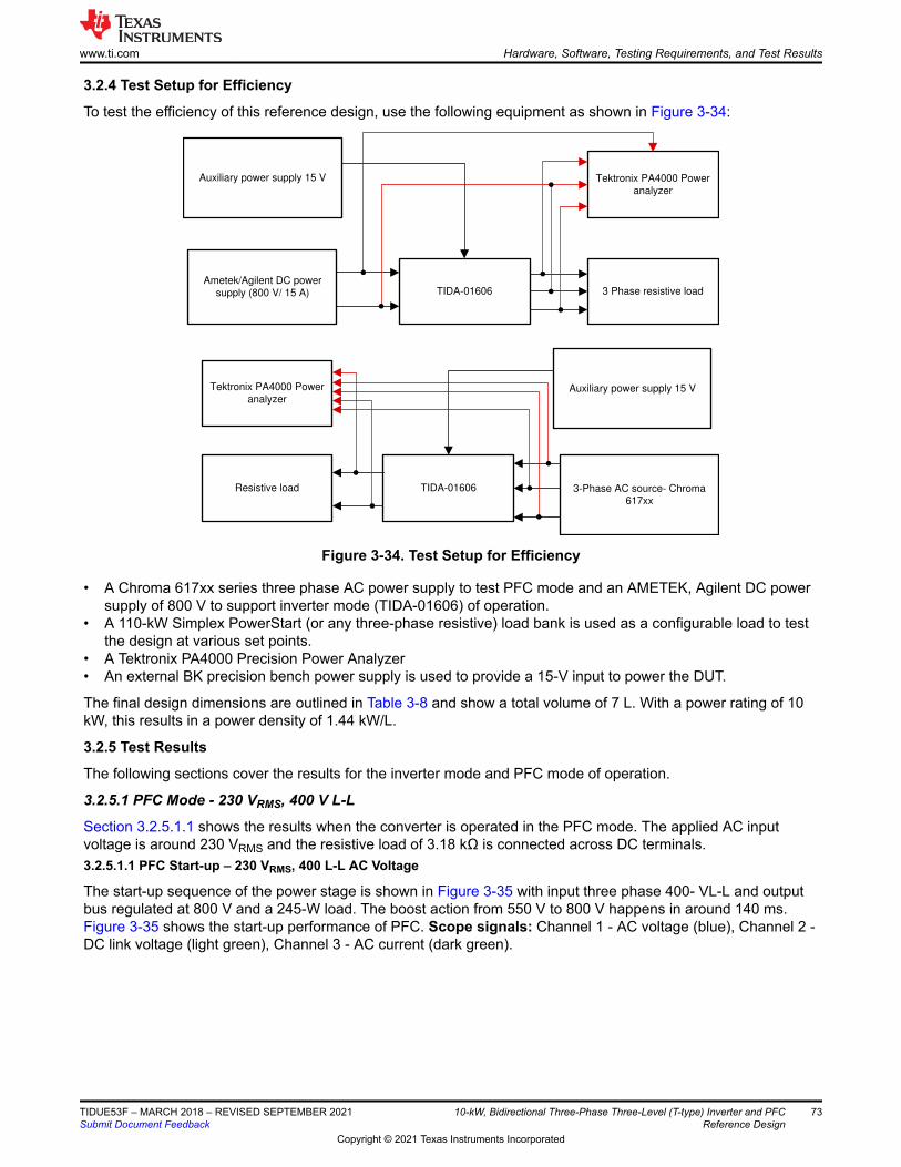
3.2.4 Test Setup for Efficiency
To test the efficiency of this reference design, use the following equipment as shown in Figure 3-34:
TIDA-01606
TIDA-01606
Tektronix PA4000 Power
analyzer
3 Phase resistive load
Auxiliary power supply 15 V
Ametek/Agilent DC power
supply (800 V/ 15 A)
Resistive load 3-Phase AC source- Chroma
617xx
Tektronix PA4000 Power
analyzerAuxiliary power supply 15 V
Figure 3-34. Test Setup for Efficiency
• A Chroma 617xx series three phase AC power supply to test PFC mode and an AMETEK, Agilent DC power supply of 800 V to support inverter mode (TIDA-01606) of operation.
• A 110-kW Simplex PowerStart (or any three-phase resistive) load bank is used as a configurable load to test the design at various set points.
• A Tektronix PA4000 Precision Power Analyzer• An external BK precision bench power supply is used to provide a 15-V input to power the DUT.
The final design dimensions are outlined in Table 3-8 and show a total volume of 7 L. With a power rating of 10 kW, this results in a power density of 1.44 kW/L.
3.2.5 Test Results
The following sections cover the results for the inverter mode and PFC mode of operation.
3.2.5.1 PFC Mode - 230 VRMS, 400 V L-L
Section 3.2.5.1.1 shows the results when the converter is operated in the PFC mode. The applied AC input voltage is around 230 VRMS and the resistive load of 3.18 kΩ is connected across DC terminals.3.2.5.1.1 PFC Start-up – 230 VRMS, 400 L-L AC Voltage
The start-up sequence of the power stage is shown in Figure 3-35 with input three phase 400- VL-L and output bus regulated at 800 V and a 245-W load. The boost action from 550 V to 800 V happens in around 140 ms. Figure 3-35 shows the start-up performance of PFC. Scope signals: Channel 1 - AC voltage (blue), Channel 2 - DC link voltage (light green), Channel 3 - AC current (dark green).
www.ti.com Hardware, Software, Testing Requirements, and Test Results
TIDUE53F – MARCH 2018 – REVISED SEPTEMBER 2021Submit Document Feedback
10-kW, Bidirectional Three-Phase Three-Level (T-type) Inverter and PFC Reference Design
73
Copyright © 2021 Texas Instruments Incorporated

Figure 3-35. PFC 230 VRMS Start-up
Care has been taken in the tuning of voltage loop to ensure that there is no overvoltage (above 800 V) during the ramp up of DC link voltage from 550 V to 800 V at start-up. The bumps in the DC link voltage during this period is because the current implementation of d-q based control in software is not fully optimized for this. Also, starting the PFC at high load can lead to overcurrent events which in turn can trip the PWMs. Hence it is advisable to start the PFC in the above mentioned test condition or lower output power. Refer to Lab 5 on possible causes for PWM trip and possible precautions the user needs to take to avoid this condition.
Hardware, Software, Testing Requirements, and Test Results www.ti.com
74 10-kW, Bidirectional Three-Phase Three-Level (T-type) Inverter and PFC Reference Design
TIDUE53F – MARCH 2018 – REVISED SEPTEMBER 2021Submit Document Feedback
Copyright © 2021 Texas Instruments Incorporated
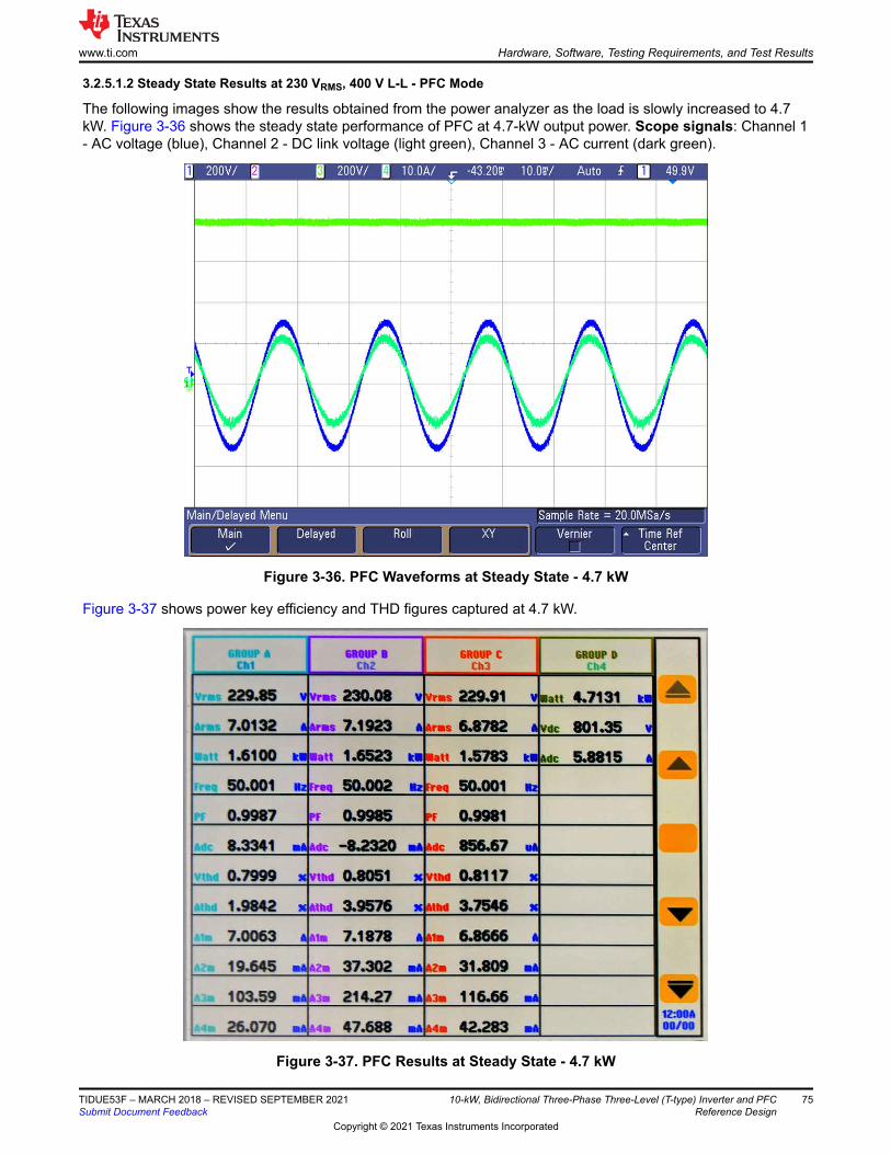
3.2.5.1.2 Steady State Results at 230 VRMS, 400 V L-L - PFC Mode
The following images show the results obtained from the power analyzer as the load is slowly increased to 4.7 kW. Figure 3-36 shows the steady state performance of PFC at 4.7-kW output power. Scope signals: Channel 1 - AC voltage (blue), Channel 2 - DC link voltage (light green), Channel 3 - AC current (dark green).
Figure 3-36. PFC Waveforms at Steady State - 4.7 kW
Figure 3-37 shows power key efficiency and THD figures captured at 4.7 kW.
Figure 3-37. PFC Results at Steady State - 4.7 kW
www.ti.com Hardware, Software, Testing Requirements, and Test Results
TIDUE53F – MARCH 2018 – REVISED SEPTEMBER 2021Submit Document Feedback
10-kW, Bidirectional Three-Phase Three-Level (T-type) Inverter and PFC Reference Design
75
Copyright © 2021 Texas Instruments Incorporated

3.2.5.1.3 Efficiency and THD Results at 220 VRMS, 50 Hz – PFC Mode
This section covers the efficiency and THD results for the converter operating in PFC mode at 220 VRMS. Table 3-5 summarizes the results obtained from power analyzer results when the load is varied from 200 W to 5 kW and DC bus voltage is kept constant at 800 V.
Table 3-5. Detailed Test Results With 220 VAC IN, 800-V DC OUT, and Varying Power LevelsPHASE - AVOLTAGE
PHASE - BVOLTAGE
PHASE - CCURRENT
PHASE - ACURRENT (A)
PHASE - BCURRENT
PHASE - CCURRENT
OUTPUTDC CURRENT (A)
OUTPUTPOWER (W)
220.3 219.94 220.15 0.398 0.573 0.405 0.25 200
220.1 219.98 220.04 0.974 1.124 0.97 0.753 600
220.09 220.02 219.98 2.55 2.64 2.48 2.018 1610
220.02 219.94 219.93 4.142 4.166 4.016 3.283 2619
220.01 219.97 219.94 5.281 5.262 5.111 4.182 3337
219.92 219.94 219.86 7.325 7.231 7.079 5.793 4624
220.01 219.97 220.03 7.89 7.81 7.76 6.278 5023
OUTPUTPOWER (W)
EFFICIENCY (%)
CURRENT-THD (PHASE-A)
CURRENT-THD (PHASE-B)
CURRENT-THD (PHASE-C)
PFC- (PHASE-A)
PFC- (PHASE-B)
FC- (PHASE-C)
200 80.93 38.88 55.46 53.44 0.8098 0.8395 0.7934
600 92.06 13.22 23.44 18.54 0.9706 0.9621 0.9678
1610 96.06 5.26 9.59 6.89 0.9944 0.9923 0.9949
2619 96.9 3.09 5.63 4.53 0.9975 0.9968 0.9977
3337 97.11 2.33 4.32 3.66 0.9982 0.9978 0.9985
4624 97.29 1.724 3.034 2.712 0.9988 0.9987 0.9990
5023 97.37 1.47 2.76 1.98 0.9992 0.9991 0.9995
Figure 3-38, Figure 3-39, and Figure 3-40 show the efficiency, THD, and power factor under different load conditions.
Output Power (W)
Effic
iency
0 1000 2000 3000 4000 500080%
82%
84%
86%
88%
90%
92%
94%
96%
98%
D006
Figure 3-38. Efficiency Results - PFC Mode at 220 VRMS
Hardware, Software, Testing Requirements, and Test Results www.ti.com
76 10-kW, Bidirectional Three-Phase Three-Level (T-type) Inverter and PFC Reference Design
TIDUE53F – MARCH 2018 – REVISED SEPTEMBER 2021Submit Document Feedback
Copyright © 2021 Texas Instruments Incorporated

Output Power (W)
TH
D
0 1000 2000 3000 4000 50000
5%
10%
15%
20%
25%
30%
35%
40%
45%
50%
D008
Figure 3-39. THD Results - PFC Mode at 220 VRMS
Output Power (W)
Pow
er
Fa
cto
r
0 1000 2000 3000 4000 50000.78
0.81
0.84
0.87
0.9
0.93
0.96
0.99
1.02
D007
Figure 3-40. Power Factor Results - PFC Mode at 220 VRMS
Figure 3-41 shows thermal performance of the board at 4.7 kW.
www.ti.com Hardware, Software, Testing Requirements, and Test Results
TIDUE53F – MARCH 2018 – REVISED SEPTEMBER 2021Submit Document Feedback
10-kW, Bidirectional Three-Phase Three-Level (T-type) Inverter and PFC Reference Design
77
Copyright © 2021 Texas Instruments Incorporated

Figure 3-41. Thermal Image at 4.7 kW
3.2.5.1.4 Transient Test With Step Load Change
In the following section, the converter is initially operating at 800 V DC link voltage at 220 VRMS AC input voltage and delivering around 400 W of output power. It is then subjected to a step load and the results are shown here for two cases. Figure 3-42 shows the transient performance when the a step load of 2 kW is applied. The voltage overshoot on the DC link voltage is around 35 V. Scope signals: Channel 1 - AC voltage (blue), Channel 2 - AC current (light green), Channel 3 - DC link voltage (dark green).
Figure 3-42. Voltage Step - 400 W → 2.4 kW
Hardware, Software, Testing Requirements, and Test Results www.ti.com
78 10-kW, Bidirectional Three-Phase Three-Level (T-type) Inverter and PFC Reference Design
TIDUE53F – MARCH 2018 – REVISED SEPTEMBER 2021Submit Document Feedback
Copyright © 2021 Texas Instruments Incorporated

Figure 3-43 shows the transient performance when the a step load of 4 kW is applied. The voltage overshoot on the DC link voltage is around 40 V. Scope signals: Channel 1 - AC voltage (blue), Channel 2 - AC current (light green), Channel 3 - DC link voltage (dark green).
Figure 3-43. Voltage Step - 400 W → 4.4 kW
Figure 3-44 shows the transient performance when the a step down load of 2 kW is applied. Scope signals: Channel 1 - AC voltage (blue), Channel 2 - AC current (light green), Channel 3 - DC link voltage (dark green).
Figure 3-44. Step Down Load Transient - 2.4 kW → 400 W
www.ti.com Hardware, Software, Testing Requirements, and Test Results
TIDUE53F – MARCH 2018 – REVISED SEPTEMBER 2021Submit Document Feedback
10-kW, Bidirectional Three-Phase Three-Level (T-type) Inverter and PFC Reference Design
79
Copyright © 2021 Texas Instruments Incorporated

Figure 3-45 shows the output voltage regulation when the input voltage is changed suddenly from 210 VAC to 175 VAC and then back to 210 VAC. Scope signals: Channel 1 - AC voltage (blue), Channel 2 - AC current (light green), Channel 3 - DC link voltage (dark green).
Figure 3-45. PFC Load Regulation to Input Voltage Change
3.2.5.2 PFC Mode - 120 VRMS, 208 V L-L
Section 3.2.5.2.1 shows the results when the converter is operated in the PFC mode. The applied AC input voltage is around 120 VRMS and the resistive load of 3.18 kΩ is connected across DC terminals. Since the results for the 230-V case have been discussed in detail, only a few results for this case are shown.
3.2.5.2.1 Steady State Results at 120 VRMS, 208 V-L-L - PFC Mode
This section shows the results obtained from the power analyzer as the load is slowly increased to 3.2 kW. The Figure 3-46 shows the steady state performance of PFC at 3.2 kW output power. Scope signals: Channel 1 - AC voltage (blue), Channel 2 - DC link voltage (light green), Channel 3 - AC current (dark green).
Hardware, Software, Testing Requirements, and Test Results www.ti.com
80 10-kW, Bidirectional Three-Phase Three-Level (T-type) Inverter and PFC Reference Design
TIDUE53F – MARCH 2018 – REVISED SEPTEMBER 2021Submit Document Feedback
Copyright © 2021 Texas Instruments Incorporated

The results in Figure 3-46 are captured at 50 Hz but these can be verified at 60 Hz as well.
Figure 3-46. PFC Waveforms at Steady State - 3.2 kW
Figure 3-47 shows power key efficiency and THD figures captured at 3.2 kW.
Figure 3-47. PFC Results at Steady State - 3.2 kW
www.ti.com Hardware, Software, Testing Requirements, and Test Results
TIDUE53F – MARCH 2018 – REVISED SEPTEMBER 2021Submit Document Feedback
10-kW, Bidirectional Three-Phase Three-Level (T-type) Inverter and PFC Reference Design
81
Copyright © 2021 Texas Instruments Incorporated

INPUT AC VOLTAGE
OUTPUT DC VOLTAGE
OUTPUT DC CURRENT
OUTPUT POWER (W)
EFFICIENCY (%) AVERAGE THD (%)
POWER FACTOR
120 608.26 0.19 116 78.61 39.33 0.81
120 608.36 1.54 936.7 94.9 5.8 0.995
120 608.15 2.13 1295 95.39 4.35 0.997
120 608.26 3.45 2100 95.71 2.71 0.998
120 608.26 4.85 2949 95.37 1.91 0.999
120 608.24 5.2 3165.7 95.29 1.85 0.999
3.2.5.2.2 Efficiency and THD Results at 120 VRMS - PFC Mode
Figure 3-48, Figure 3-49, and Figure 3-50 show the efficiency, THD, and power factor under different load conditions for the PFC operating at 120 VRMS.
Output Power (W)
Effic
iency
0 500 1000 1500 2000 2500 3000 350075%
80%
85%
90%
95%
100%
D003
Figure 3-48. Efficiency Results - PFC Mode at 120 VRMS
Output Power (W)
TH
D
0 500 1000 1500 2000 2500 3000 35000
5%
10%
15%
20%
25%
30%
35%
40%
D005
Figure 3-49. THD Results - PFC Mode at 120 VRMS
Hardware, Software, Testing Requirements, and Test Results www.ti.com
82 10-kW, Bidirectional Three-Phase Three-Level (T-type) Inverter and PFC Reference Design
TIDUE53F – MARCH 2018 – REVISED SEPTEMBER 2021Submit Document Feedback
Copyright © 2021 Texas Instruments Incorporated

Output Power (W)
Pow
er
Fa
cto
r
0 500 1000 1500 2000 2500 3000 35000.8
0.85
0.9
0.95
1
D004
Figure 3-50. Power Factor Results - PFC Mode at 120 VRMS
3.2.5.3 Inverter Mode
Section 3.2.5.3.1 shows the results when the converter is operated in the inverter mode. The applied DC input voltage is 800 V and the resistive load is connected across AC terminals.
3.2.5.3.1 Inverter Closed Loop Results
The inverter is tested in the closed current loop in Lab 3 where the current reference is varied by changing the variable TINV_idRef_pu from the watch window. Setting this value to around 0.35 pu should deliver around 3.5 kW of power at the AC terminals. Figure 3-51 shows closed current loop operation and the efficiency results obtained. Scope signals: Channel 1 - DC link voltage (blue), Channel 2 - AC voltage (light green), Channel 3 - AC current (dark green).
Figure 3-51. Inverter Closed Current Loop Waveforms
www.ti.com Hardware, Software, Testing Requirements, and Test Results
TIDUE53F – MARCH 2018 – REVISED SEPTEMBER 2021Submit Document Feedback
10-kW, Bidirectional Three-Phase Three-Level (T-type) Inverter and PFC Reference Design
83
Copyright © 2021 Texas Instruments Incorporated

Figure 3-52 shows power key efficiency and THD figures captured with power analyzer at 3.8 kW.
Figure 3-52. Inverter Closed Current Loop Results
3.2.5.3.2 Efficiency and THD Results - Inverter Mode
This section covers the efficiency and THD results for the converter operating in inverter mode at 800 V DC link. Table 3-6 summarizes the results obtained from power analyzer results when the load is varied from up to 3.8 kW.
Table 3-6. Detailed Test Results With 220 VAC OUT, 800-V DC IN, and Varying Power LevelsOUTPUT POWER (WATTS)
EFFICIENCY (%) CURRENT-THD (PHASE-A)
CURRENT-THD (PHASE-B)
CURRENT-THD (PHASE-C)
POWER FACTOR
1563 97.4 1.37 0.92 0.78 0.999
2555 97.6 1.01 0.85 0.74 0.999
3761 97.8 0.6 0.77 0.63 0.999
Hardware, Software, Testing Requirements, and Test Results www.ti.com
84 10-kW, Bidirectional Three-Phase Three-Level (T-type) Inverter and PFC Reference Design
TIDUE53F – MARCH 2018 – REVISED SEPTEMBER 2021Submit Document Feedback
Copyright © 2021 Texas Instruments Incorporated

Figure 3-53 and Figure 3-54 show the efficiency and THD under different load conditions for the inverter operating at 800 VDC.
Output Power (W)
Effic
iency
1500 1750 2000 2250 2500 2750 3000 3250 3500 375097.4%
97.45%
97.5%
97.55%
97.6%
97.65%
97.7%
97.75%
97.8%
D001
Figure 3-53. Efficiency Results - Inverter Mode
Output Power (W)
TH
D
1500 1750 2000 2250 2500 2750 3000 3250 3500 37500.6%
0.8%
1%
1.2%
1.4%
D002
Figure 3-54. THD Results - Inverter Mode
www.ti.com Hardware, Software, Testing Requirements, and Test Results
TIDUE53F – MARCH 2018 – REVISED SEPTEMBER 2021Submit Document Feedback
10-kW, Bidirectional Three-Phase Three-Level (T-type) Inverter and PFC Reference Design
85
Copyright © 2021 Texas Instruments Incorporated

3.2.5.3.3 Inverter - Transient Test
Figure 3-55 shows load transient performance of the inverter from no load to 3.2 kW by applying a current step in the current loop. Scope signals: Channel 1 - DC link voltage (blue), Channel 2 - AC voltage (light green), Channel 3 - AC current (dark green).
Figure 3-55. Inverter Current Loop Transient
Hardware, Software, Testing Requirements, and Test Results www.ti.com
86 10-kW, Bidirectional Three-Phase Three-Level (T-type) Inverter and PFC Reference Design
TIDUE53F – MARCH 2018 – REVISED SEPTEMBER 2021Submit Document Feedback
Copyright © 2021 Texas Instruments Incorporated

3.2.6 Open Loop Inverter Test Results
The system efficiency results are detailed in Table 3-7.
Table 3-7. System Efficiency ResultsPOWER RATING 10% 20% 30% 40% 50% 60% 70% 80% 90% 100%
600-V input 95.6% 97.43% 97.74% 97.82% 97.79% 97.79% 97.79% 97.79%
800-V input 92.64% 96.55% 97.87% 98.31% 98.42% 98.47% 98.51% 98.54% 98.7% 98.22%
1000-V input 92.37% 96.55% 97.95% 98.52% 98.77% 98.95% 99.01% 99.06% 99.08% 99.02%
Figure 3-56 shows the inverter efficiency graph.
Power Level ( of 10 kW)
Effic
iency (
)
0 10% 20% 30% 40% 50% 60% 70% 80% 90% 100% 110% 120%92
93
94
95
96
97
98
99
100
D002
600 VIN
800 VIN
1000 VIN
Figure 3-56. Inverter Efficiency
Table 3-8 shows the dimensions of the system.
Table 3-8. System DimensionsAXIS DIMENSION
X 350 mm
Y 200 mm
Z 100 mm
Volume 7 liters
The total energy density of the design is 10 kW/7L, or 1.43 kW/L.
www.ti.com Hardware, Software, Testing Requirements, and Test Results
TIDUE53F – MARCH 2018 – REVISED SEPTEMBER 2021Submit Document Feedback
10-kW, Bidirectional Three-Phase Three-Level (T-type) Inverter and PFC Reference Design
87
Copyright © 2021 Texas Instruments Incorporated

4 Design Files4.1 SchematicsTo download the schematics, see the design files at TIDA-01606.
4.2 Bill of MaterialsTo download the bill of materials (BOM), see the design files at TIDA-01606.
4.3 PCB Layout Recommendations4.3.1 Layout Prints
To download the layer plots, see the design files at TIDA-01606.
4.4 Altium ProjectTo download the Altium Designer® project files, see the design files at TIDA-01606.
4.5 Gerber FilesTo download the Gerber files, see the design files at TIDA-01606.
4.6 Assembly DrawingsTo download the assembly drawings, see the design files at TIDA-01606.
5 TrademarksTI E2E™, Delfino™, TMS320C2000™, PowerPAD™, C2000™, and are trademarks of Texas Instruments.Altium Designer® is a registered trademark of Altium LLC or its affiliated companies.All trademarks are the property of their respective owners.
6 About the AuthorsMANISH BHARDWAJ is a systems application engineer with C2000 Microcontrollers System Solutions Group at Texas Instruments, where he is responsible for developing reference design solutions for digital power, motor control, and solar power applications. Before joining TI in 2009, Manish received his Masters of Science in Electrical and Computer Engineering from Georgia Institute of Technology, Atlanta and his Bachelor of Engineering from Netaji Subhash Institute of Technology, University of Delhi, India.
BART BASILE is a systems architect in the Grid Infrastructure Solutions Team at Texas Instruments, where he focuses on renewable energy and EV infrastructure. Bart works across multiple product families and technologies to leverage the best solutions possible for system level application design. Bart received his bachelors of science in electronic engineering from Texas A&M University.
HARISH RAMAKRISHNAN is a systems engineer at Texas Instruments India, where he is responsible for developing reference design solutions for Grid Infrastructure.He received his bachelors degree in electrical engineering from National Institute of Technology Durgapur, India and masters degree from Texas A&M University.
MURALI KRISHNA PACHIPULUSU is a systems engineer at Texas Instruments, where he is responsible for developing reference design solutions for the industrial segment. Murali brings to this role his experience in analog and digital power electronics converters design to this role. Murali earned his master of technology (M.Tech) from the Indian Institute of Technology in Delhi.
Design Files www.ti.com
88 10-kW, Bidirectional Three-Phase Three-Level (T-type) Inverter and PFC Reference Design
TIDUE53F – MARCH 2018 – REVISED SEPTEMBER 2021Submit Document Feedback
Copyright © 2021 Texas Instruments Incorporated

7 Revision HistoryNOTE: Page numbers for previous revisions may differ from page numbers in the current version.
Changes from Revision E (July 2021) to Revision F (September 2021) Page• Missing TIDA-01606 ISOHVCARD board added for evaluation purposes in the Test Hardware Required
section.............................................................................................................................................................. 39
Changes from Revision D (April 2021) to Revision E (July 2021) Page• Updated Voltage Loop Plant Frequency Response Measured vs Modelled image..........................................36
Changes from Revision C (March 2018) to Revision D (April 2021) Page• Revision D of the design guide is updated to reflect changes in the control design, hardware and software,
and the testing and results..................................................................................................................................1• Added Control Design section.......................................................................................................................... 32• Updated Required Hardware and Software section......................................................................................... 39• Updated Testing and Results section............................................................................................................... 46
Changes from Revision B (May 2020) to Revision C (August 2020) Page• Changed title to 10-kW, Three-Level, Three-Phase T-Type Inverter Reference Design for Solar String
Inverters..............................................................................................................................................................1
Changes from Revision A (March 2019) to Revision B (May 2020) Page• Added To obtain an attenuation factor of 10%, and using the earlier derived values, the value of r can be
evaluated to be: ............................................................................................................................................... 18
Changes from Revision * (March 2018) to Revision A (March 2018) Page• Updated block diagram Figure 1. TIDA-01606 Block Diagram: "F28004x Control Card" to "F28377D Control
Card"...................................................................................................................................................................1
www.ti.com Revision History
TIDUE53F – MARCH 2018 – REVISED SEPTEMBER 2021Submit Document Feedback
10-kW, Bidirectional Three-Phase Three-Level (T-type) Inverter and PFC Reference Design
89
Copyright © 2021 Texas Instruments Incorporated

IMPORTANT NOTICE AND DISCLAIMERTI PROVIDES TECHNICAL AND RELIABILITY DATA (INCLUDING DATASHEETS), DESIGN RESOURCES (INCLUDING REFERENCEDESIGNS), APPLICATION OR OTHER DESIGN ADVICE, WEB TOOLS, SAFETY INFORMATION, AND OTHER RESOURCES “AS IS”AND WITH ALL FAULTS, AND DISCLAIMS ALL WARRANTIES, EXPRESS AND IMPLIED, INCLUDING WITHOUT LIMITATION ANYIMPLIED WARRANTIES OF MERCHANTABILITY, FITNESS FOR A PARTICULAR PURPOSE OR NON-INFRINGEMENT OF THIRDPARTY INTELLECTUAL PROPERTY RIGHTS.These resources are intended for skilled developers designing with TI products. You are solely responsible for (1) selecting the appropriateTI products for your application, (2) designing, validating and testing your application, and (3) ensuring your application meets applicablestandards, and any other safety, security, or other requirements. These resources are subject to change without notice. TI grants youpermission to use these resources only for development of an application that uses the TI products described in the resource. Otherreproduction and display of these resources is prohibited. No license is granted to any other TI intellectual property right or to any third partyintellectual property right. TI disclaims responsibility for, and you will fully indemnify TI and its representatives against, any claims, damages,costs, losses, and liabilities arising out of your use of these resources.TI’s products are provided subject to TI’s Terms of Sale (https:www.ti.com/legal/termsofsale.html) or other applicable terms available eitheron ti.com or provided in conjunction with such TI products. TI’s provision of these resources does not expand or otherwise alter TI’sapplicable warranties or warranty disclaimers for TI products.IMPORTANT NOTICE
Mailing Address: Texas Instruments, Post Office Box 655303, Dallas, Texas 75265Copyright © 2021, Texas Instruments Incorporated