Topic 12 Testing Based on slides/material by… Testing Logic ...

~- 6 . .
Introduction to Logic Testing
Z = XI . X2 .
The output z of an OR gate with inputs Xl and X2 is 1 ifand only ifany of itsinputs are 1, and can be expressed as
z = Xl + X2 .
The output z ora NOT gate or an inverter with input X is 1 ifand only ifitsinput is 0, and can be expressed as
z = x .
The output z of a NAND gate with inputs Xl and X2 is 1 ifand only if any ofits inputs are 0, and can be expressed as
The development of computers has been stimulated greatly by integrated -
circuit technology . Circuit density has increased dramatically , and the cost
of devices has decreased as their performance has improved . With these
developments , reliability has become increasingly important . However ,
with the advent of very - large - scale integration ( VLSI ) , testing has come up
against a wall of , ' intractability " and is at a standstill . Since the gate density
of V L S I circuits is increasing much more rapidly than the number of access
terminals , the ability to generate test patterns and to process fault simulations
is deteriorating . The difficulty can be reduced by the development of
faster and more efficient algorithms for test - pattern generation or by the use
of design techniques to enhance testability .
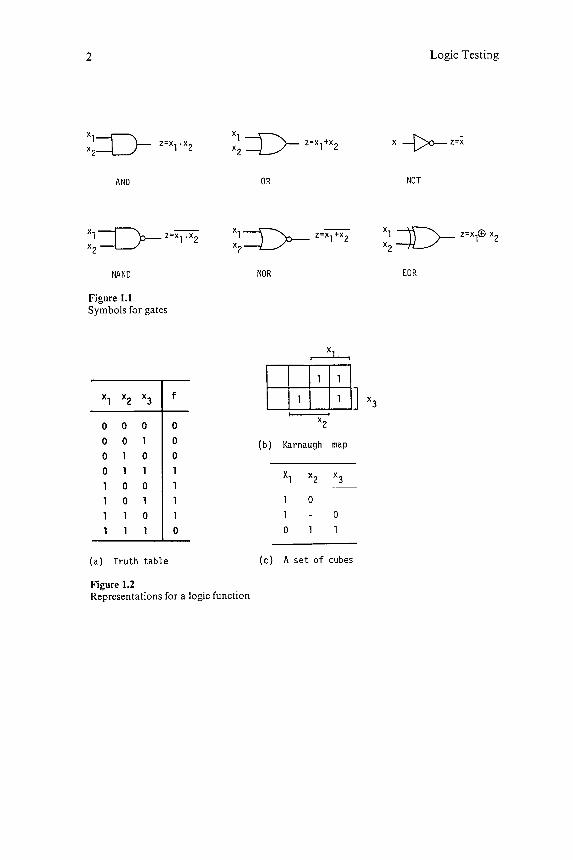
1 . 1 Logic Circuits
Logic circuits are constructed by interconnecting elements called gates
whose inputs and outputs represent only the values denoted by 0 and 1 .
Some common gates are AND , OR , NOT , NAND , NOR , and EOR
( Excl .usive - OR ) ; their symbols are shown in figure 1 . 1 . The output of each
gate can be represented by a logic function or a Boolean function of the
inputs . The terms logic and Boolean are often used to denote the same
meaning . A logic function can be specified by a truth table , a Karnaugh
map , or a set of cubes . Figure 1 . 2 demonstrates these three forms . The
Boolean ( logic ) operations . , + , and - correspond to AND , OR , and NOT ,
respectively .
The output z of an AND gate with inputs Xl and Xl is 1 if and only ifboth
of its inputs are 1 simultaneously , and can be expressed as
Logic Testing
1- 1___I~j-:-JI 11 I 11 IJ x3
2
Xl -Ij~ - z=xl+x2X 2 --L/-Xl-~ -x 2-LJ- x - { > o- z=xZ=X1oX2
NOTAND OR
x .=[~=))- - x =~~~: ).- - x =~l=~)-, z=xix2' z=x,+x2 ' z=x,(l) x2x2 x2 x2EORNAND
Figure 1.1
NOR
. Xl .
I X .2(b) Karnaugh map
�
11 0
11�
(c) A set of cubes(a) Truth table
Figure 1.2Representations for a logic function
Symbols for gates
Xl X2 X3-
0
-
Xl x2 x3 f
0 0 0 0-0 0 1 00 1 0 00 1 1 11 0 0 11 0 1 11 1 0 11 1 1 0
3Introduction to Logic Testing
z = x; ~ = Xl + X2'
The output z ora NOR gate with inputs Xl and X2 is 1 ifand only ifboth ofits inputs are 0, and can be expressed as
z = Xl + X2 = Xl ' X2 '
The output z of an EaR gate with inputs Xl and X2 is 1 if and only ifits inputare not simultaneously equal , and can be expressed as
Z = X I Xl + X I Xl = Xl EB Xl '
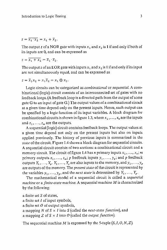
Logic circuits can be categorized as combinational or sequential. Acom -
binational (logic ) circuit consists of an interconnected set of gates with no
feedback loops . (A feedback loop is a directed path from the output of somegate G to an input of gate G .) The output values of a combinational circuitat a given time depend only on the present inputs . Hence, each output can
be specified by a logic function of its input variables . A block diagram forcombinational circuits is shown in figure 1.3, where Xl " ' " Xn are the inputs
and Zl , . . . , Zm are the outputs .
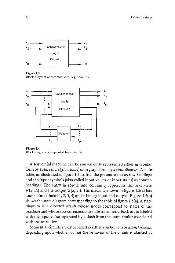
A sequential (logic ) circuit contains feedback loops . The output values ata given time depend not only on the present inputs but also on inputs
applied previously . The history of previous inputs is summarized in thestate of the circuit . Figure 1.4 shows a block diagram for sequential circuits .
A sequential circuit consists of two sections: a combinational circuit and amemory circuit . The circuit of figure 1.4 has n primary inputs Xl " ' " Xn; m
primary outputs Zl , . . . , Zm; P feedback inputs YI , . . . , Yp; and p feedback
outputs Y1, . . . , Yp. Y1, . . . , Yparealsoinputstothememory , and Yl " " ' YPare outputs of the memory . The present state of the circuit is represented by
the variables Yl , . . . , Yp, and the next state is determined by Y1, . . . , Yp.The mathematical model of a sequential circuit is called a sequential
machine or a finite -state machine. A sequential machine M is characterized
by the following :
a finite set S of states,
a finite set I of input symbols ,a finite set 0 of output symbols ,
a mapping N of S x I into S (called the next -state function ), anda mapping Z of S x I into 0 (called the output function ).
The sequential machine Misexpressed by the 5-tuple (S, 1, 0 , N , Z ).
Xl
x2 Combinational
Logic
Circuit
xn
4 Logic Testing
Figure 1.3
Zm
Figure 1.4Block diagram of sequential logic circuits
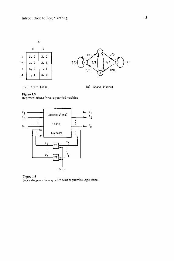
A sequential machine can be conveniently represented either in tabular
form by a state table (flow table) or in graph form by a state diagram. A statetable, as illustrated in figure 1.5(a), lists the present states as row headingsand the input symbols (also called input values or input states) as columnheadings. The entry in row Si and column Ij represents the next stateN(Si' Ij) and the output Z(Si' Ij). The machine shown in figure 1.5(a) hasfour states (labeled 1, 2, 3, 4) and a binary input and output. Figure 1.5(b)shows the state diagram corresponding to the table of figure 1.5(a). A statediagram is a directed graph whose nodes correspond to states of themachine and whose arcs correspond to state transitions . Each arc is labeled
with the input value separated by a slash from the output value associatedwith the transition .
Sequential circuits are categorized as either synchronous or asynchronous,depending upon whether or not the behavior of the circuit is clocked at
Block diagram of combinational logic circuits
Zl
z2
Combinational. - .. .. Logic .. Circuit '. I. .
Yl Yl. ,I Memory '. IYp I I Yp
Zl
z2
I
II
Zm
Xlx2
Xn
Combinational
I I
I
X I Logic : zn m
: Circuit :. .
Yl YlI I
I I
I .
Yp Yp
clock
5Introduction to Logic Testing
x
0 1
1/ 0 1/ 1
1
2
3
4
(b) State diagram
Figure 1.6Block diagrarrI for a synchronous sequential logic circuit
(a) State table
Figure 1.5Representations for a sequential machine
Zlz2
Xlx2
2, 0 3, 03, 0 2, 14, 0 1, 11, 1 4. 0

6 Logic Testing
SR
S Q Q 00 01 11 10
clock CP - I I I - 11 IR Q 111101 - 11 I
(a) SR flip - flop
JK
J Q Q 00 01 11 10
CP - I I o 11 11 IK Q 1111 1 111
(b) JK flip - flop
T
T Q Q 1
- ornlCP Q1 1 o
(c ) T flip - flop
D
D Q Q 1
- o rnlCP Q1 o 1
( d) D flip - flop
Figure 1.7Representations for flip -flops

Introduction to Logic Testing 7
clock
Q
R Q
s
Figure 1.8Realization of the SR flip-flop
Figure 1.9Block diagram for asynchronous sequential logic circuit
discrete instants of time . The operation of synchronous sequential circuits is
control led by a synchronizing pulse signal called a clock pulse or simply aclock. The clock is usually applied to the memory portion of the circuit .
Figure 1.6 is a block diagram for synchronous circuits . A series of bistable
memory elements called clocked flip -flops (FF ) are used in synchronouscircuits . The most popular memory elements are the D (Delay ), T (Trigger ),
SR (Set-Reset), and JK flip -flops shown in figure 1.7. Figure 1.8 shows arealization of the SR flip -flop . Other flip -flops can be similarly constructedfrom cross-coupled NAND or NOR gates.
The behavior of an asynchronous circuit is not synchronized ; it is unclocked. Each feedback line is assumed to have a finite , positive , pure delay,
as is shown in figure 1.9. Proper operation of such an asynchronous circuit
requires the following conditions .
Xl zl
x2 . . Corobinational z2I I
I Logic I. I
X Z
n Circuit m
I I
. .
I .
.
.
.
8 Logic Testing
. Because of delays, a combinational circuit may produce a transient error
or spike, called a hazard. Such an error , if applied to the input of anunclocked flip -flop or latch , may result in a permanent incorrect state.
Hence the combinational logic portion of the circuit should be designed tobe hazard -free.
. The inputs are constrained so as to change only when the memory
elements are all in stable conditions (Yi = Yi for all i ). This is called thefundamental mode operation .
. A situation whereby more than one state variable must change in thecourse of a transition is called a race condition . If correct behavior of the
circuit depends upon the outcome of the race, then it is called a critical race.
To ensure that the operation of the circuit is not affected by transients , thecritical race should be avoided by making the proper state assignment .
1.2 Fault Modeling
L <?gic gates are realized by transistors , which are classified into bipolartransistors and metal oxide semiconductor field -effect transistors
(MOSFET, or simply MOS). The logic families based on bipolar transistorsare transistor-transistor logic (TTL), emitter-coupled logic (ECL), and soforth . Some logic families based on MOSFET are p-channel MOSFET
(p-MOS), n-channel MOSFET (n-MOS), and complementary MOSFET(CMOS). Although ECL and TTL are important for high-speed applications
, their integration sizes are limited by the heat generated by theirheavy power consumption and by large gate sizes. In contrast , the MOS
logic families are well suited for LSI or VLSI , because larger integrationscan be obtained with them than with bipolar logic families . Most LSI andVLSI circuits of today are implemented by MOS . However , the increasinguse of MOS technology for LSI and VLSI circuits has introduced new
testing problems , as will be seen later in this chapter .A fault of a circuit is a physical defect of one or more components . Faults
can be classified as logical or parametric. 'A~ logical fault is one th~t cause~the logic function of a circuit e1emento( ~~" iriputsignalt-o be changed t-'dsome other lo-gicfunctiolii a parametric fault alters the magnitude of a
. " '
circuit parameter , causing a change in some factor such as circuit speed,current , or voltage .
Circuit malfunctions associated with timing are due mainly to circuit
Introduction to Logic Testing 9
----t)~o-..--
z = xz x
Collectorx
(a) Bipolar realization (b) Logic symbol
delays . Those faults that relate to circuit delays such as slow gates are called
delay faults . Usually , delay faults only affect the timing operation of the
circuit , which may cause hazards or critical races .
F ~ ults that are present in some intervals of time and absent in others are
intermittent faults . Faults that are always present and do not occur , disappear
, or change their nature during testing are called permanent faults or
solid faults . Although many intermittent faults eventually become solid ,
the early detection of intermittent faults is very important to the reliable
operation of the circuit . However , there are no reliable means of detecting
their occurrence , since such a fault may disappear when a test is applied . In
this book , we will consider mainly logical and solid faults .
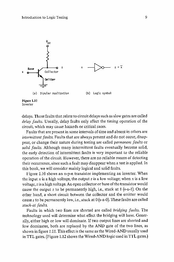
Figure 1. 10 shows an n - p - n transistor implementing an inverter . When
the input x is a high voltage , the output z is a low voltage ; when x is a low
voltage , z is a high voltage . An open collector or base of the transistor would
cause the output z to be permanently high , i .e., stuck at 1 (sa - 1). On the
other hand , a short circuit between the collector and the emitter would
cause z to be permanently low , i .e., stuck at 0 (sa -O). These faults are called
stuck -at faults .
Faults in which two lines are shorted are called bridging faults . The
technology used will determine what effect the bridging will have . Generally
, either high or low will dominate . If two output lines are shorted and
low dominates , both are replac .ed by the AND gate of the two lines , as
shown in figure 1. 11 . This effect is the same as the Wired -AND usually used
in TTL gates . (Figure 1. 12 shows the Wired - AND logic used in TTL gates .)
Figure 1.10Inverter

10 Logic Testing
x
Y f
9
z
w
x
yf
9w
(a) (b)
Figure 1.11
- f = x- : y.-z:-:-w
w
x
y
z
Figure 1.12Wired-AND used in TTL gates
AND-type bridging fault

Introduction to Logic Testing 11
x 1 - -f- - ~ - z = -x--:-x-x 2 - -{- - . , / "' 1 2
I
I ~
(a) Logic symbol N - I' ~ l-\ ,C, ,-/!)f.'\~} tiC IC ' v " ,V i
DO . " :
f" I " i\ ..-.. .- .. ~C\"' - JY \ - - - Co I ' "
~ ' /1(JO r ~", u -t
r v --::- L ::: } -:Y/ / \ , ~ I .,7z - .-.!_~ - / ~ ~
CD --- I ! - ~)- C i\ ~i Ji ivl- i. 7 ~.//c;:2'
xl ' I } / .,! i
o-l___----i ~ L.J , "'" I
@) - ;I } i I ] Jx2 j ,/
!
i I,-I \...~j I 1/ d (~- ' .-- / . v
(b) MOS realization /[ ) ,/ ,,' , ~" /O!/I '/. / ; ! /A{) ) :; ; .'~t,::; L.il '--'~/ l ::..; ;; ,-
FIgure 1.13 . ' r ;1 J . ' r ,-, - ~ .. : C "' i "-/CMOS two-Input NAND gate I ,j / -i ;:/\ 6 "~ ) liU-- .s VJ } ! / , :;
If high dominates , both of the lines are replaced by the OR gate of the twolines . The ECL gate has the feature that the OR of the outputs can be
realized simply by tying together these outputs . Hence, in logic circuits
implemented by ECL gates, bridging faults cause the affected signals to beO Red .
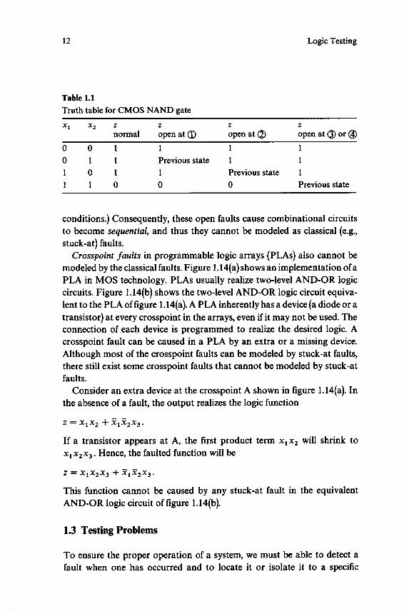
For most practical purposes, logical faults are success fully modeled bystuck -at faults or bridging faults . However , not all faults can be modeled bythese classical faults . This is illustrated by the following examples. Figure
1.13 shows a CMOS two -input NAND gate with p-MOS and n-MOS
FETs . The output z is a low voltage if and only ifboth inputs Xl and X2 are
high. In figure 1.13, four possible open faults (numbered 1 through 4) areindicated . The first fault , numbered 1, is caused by an open, or missing , p-
channel xl -input pull -up transistor . Under this fault , when the input Xl islow and the input X2 is high , the output z becomes an undesired , high -
impedance state and retains the logic value of the previous output state. Thelength of time the state is retained , however , is determined by the leakage
current at the node. (Table 1.1 is the truth table for the two-input CMOSNAND gate for both the fault - free condition and the three faulted
12 Logic Testing
Table 1.1
Truth table for CM OS NAND gate
Xl X2 Z Z Z Z
normal open at CD open at C2) open at Q) or @
0 0 1 1 1 1
0 1 1 Previous state 1 1
1 0 1 1 Previous state 1
1 1 0 0 0 Previous state
conditions.) Consequently, these open faults cause combinational circuitsto become sequential, and thus they cannot be modeled as classical (e.g.,stuck-at) faults.
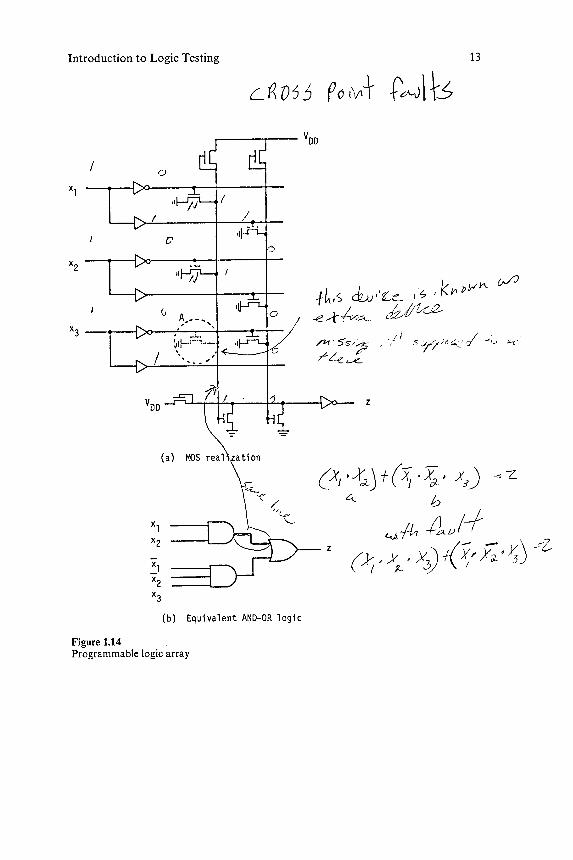
Crosspoint faults in programmable logic arrays (PLAs) also cannot bemodeled by the classical faults. Figure 1.14(a) shows an implementation ofaPLA in MOS technology . PLAs usually realize two -level AND -OR logic
circuits. Figure 1.14(b) shows the two-level AND-OR logic circuit equivalent to the PLA of figure 1.14(a). A PLA inherently has a device (a diode or a
transistor) at every crosspoint in the arrays, even if it may not be used. Theconnection of each device is programmed to realize the desired logic . Acrosspoint fault can be caused in a PLA by an extra or a missing device.Although most of the crosspoint faults can be modeled by stuck -at faults ,there still exist some crosspoint faults that cannot be modeled by stuck -atfaults .
Consider an extra device at the crosspoint A shown in figure 1.14(a). Inthe absence of a fault , the output realizes the logic function
Z = XIX2 + X1X2X3 .
If a transistor appears at A, the first product term XIX2 will shrink toX I X2 X3 ' Hence , the faulted function will be
Z = XIX2X3 + XIX2X3 .
This function cannot be caused by any stuck -at fault in the equivalent
AND-OR logic circuit of figure 1.14(b).
1.3 Testing Problems
To ensure the proper operation of a system, we must be able to detect afault when one has occurred and to locate it or isolate it to a specific
+~JS ~I'~L- ,'~ J KY' "V./Y'I.-J--L /- /;1......17-.e ..- ,( ~ c?;;Z/i/ v '"-"-"
Introduction to Logic Testing
L ri V ) j P () 1\\;1+ f ~ \ t . . s
13
Voo
A - - ,# ,
X " ,
3 , .. 1...I L , . . . . ,
I ' ~ . . . . . -, ' .
\
I \ ,, . . .' . ~
0
Xl
0
X2CIJJ
J 6
z
(a)
(XI J~J +(~ '~j A3)~ b~ - z.
~~ Aul-f(~"')';I...' Y:!J) +(~ I' ~. ~JXlX2 ,::,,7.- 1-/-xlx2x3
(b) Equivalent AND-OR logic
Figure 1.14Programmable logic array

14 Logic Testing
s - a - l
=tf ~)--~~=D ~ cA
c
(b) Faulty AND gate.
component - preferably an easily replaceable cine. The former procedure iscalled fault detection, and the latter is called fault location , fault isolation ,
or fault diagnosis. These tasks are accomplished with tests. A test is aprocedure to detect and/or locate faults . Tests are categorized as fault -detection tests or fault diagnostic tests. A fault -detection test tells onlywhether a circuit is faulty or fault -free; it tells nothing about the identity of a
fault if one is present. A fault diagnostic test provides the location and thetype of a fault and other information . The quantity of information providedis called the diagnostic resolution of the test; a fault -detection test is a faultdiagnostic test of zero diagnostic resolution .
Logic circuits are tested by applying a sequence of input patterns that
produce erroneous responses when faults are present and then comparing
the responses with the correct (expected) ones. Such an input pattern usedin testing is called a test pattern . In general, a test for a logic circuit consists
of many test patterns . They are referred to as a test set or a test sequence. Thelatter term , which means a series of test patterns , is used if the test patterns
must be applied in a specific order . Test patterns , together with the outputresponses, are sometimes called test data.
Figure 1.15(a) shows a fault -free AND gate. Figure 1.15(b) shows a faultyAND gate in which input A is stuck -at-1. The input pattern applied to thefault -free AND gate has an output value of O. In contrast , the output valueof the faulty AND gate is 1, since the stuck -at-1 fault on A creates the
erroneous response. There is a definite difference between the faulty gateand the fault -free gate. Therefore , the pattern 01 shown in figure 1.15 is a test
pattern for the A sa - 1 fault .If there exists only one fault in a circuit , it is called a single fault . If there
exist two or more faults at the same time , then the set of faults is called a
multiple fault . For a circuit with k lines, there are at most 2k possible single
A
B
(a) Fault- free AND gate
Figure 1.15Test for stuck-at fault

Introduction to Logic Testing 15
L ./-// ' If ), I!J~ -' / kxl A B F r':JI ,,-I .s' J /"p LR r '-"J/ I---> .:::.. t=-
o : 1 cE ;==:::O ~ Z Jut J }1'1u/f f?\ul-f-{ -::3k"'I...J/\x 2 o-_.....~._.~=~=:==1~~~~:::)J----~.. ]
Figure 1.16 I JAlo + p) ) t~ ef {jl. r~ / tv'ytj
Table 1.2 fJ. ,~ ~ d::tL.A~ c;..--{Ll..c;-All single stuck faults
Xl X2 z A/O B/O C/O D /O E/OF /O All Bl1 Cl1 dll Ell Fl1
0 0 1 1 1 1 1 1 0 - 0 - 0 1 1 1 1
0 1 1 1 1 1 1 1 0 1 0 1 1 1 1
1 0 0 1 - 1 - 0 0 - 1 0 0 0 0 ~ 1 0 , 1
1 1 1 1 1 - 0 - 0 1 - 0 1 11 1 ~ O 1 , I
~ """'~) ; .:.. J. ~ ..~)v-1-' -~ r-- ~J.L--.,,~-~~, -,,~I/nJ""; I.". / 1 ~ V I; ! ./ !-~~1. ~ OJ!'"r Z It ' f~-v"I.( .$ tOl..-}\ c)~(;{!)r :5. Cj; /" '/10+ ~ ~::?~7~ UI ~ :AIJ , ~ " I '\ + $ v ~ J"I \ ", \) ~ J '
stuck -at faults . For multiple faults , the number of possible faults increases. k ..;Z. ' K (;:- 5 'v. A- L... / '~ v J '" ~
dramatIcally to 3 - 1,- sInce anY-line may be fault -free, sa -O, or s-a- 1. A
circuit with 100 lines would contain approximately 5 x 1047 faults . Thiswould be far too many faults to assume, and hence testing for multiple faultswould be impractical . However , for most approach es the model of a singlestuck -at fault has proved to provide the best practical basis. For example ,every complete single-fault -detection test set in any internal fanout -free
combinational circuit is known to cover at least 98 percent of all multiple
faults made up of six or fewer faults (Agarwal and Fung 1981).Since several different faults often may cause a circuit to malfunction in
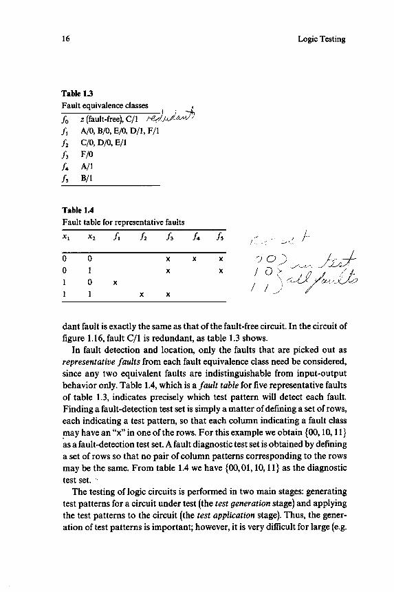
precisely the same way, it is convenient to group these equivalent faults (orindistinguishable faults) into equivalence classes. In the circuit shown infigure 1.16, there are six signal lines (nets); hence, there are at most twelvepossible single stuck -at faults . Table 1.2 illustrates a truth table with~olumns listing all possible single stuck -at faults and rows indicating allinput patterns , where a line A stuck -at -O fault , for example , is denoted asA/O. As can be seen from table 1.2, the malfunctions caused by AIO, BIO, EIO,Dl1 , and F II are all the same, so they are grouped together in a faultequivalence class. Similarly , CIO, DIO, and Ell are grouped together , asshown in table 1.3 . A fault is called redundant if its presence causes no
malfunction . In other words , the output function of a circuit with a red un -
16 Logic Testing
Table 1.3
Fault equivalence classes . A
10 z (fault-free), Cj1 f'V~)p./~'o/ ,;;D11 AjO, BjO, EjO, Dj1 , F j1
12 CjO, DjO, Ej1
13 FjO
14 Aj1
15 Bj1
Table 1.4
Fault table for representative faultsi
Xl X2 11 12 13 14 Is ~' - ; ! -I , e / - ~ ". !
0 0 X X X ,:) 0 ) . I~". dO 1 j cJ I ~'-'!/"" ../ -ilA ,X X "" / 1, 11 ,' , ,...,{ 1/ ; / ! i
1 0 X \ C-;:--.r Y v ,:" ( ( ; ' {..-')/ / ) ..-/~-,::/ ' " :.-./l ..
1 1 x X ,J P'
dant fault is exactly the same as that of the fault -free circuit . In the circuit offigure 1.16, fault CjI is redundant , as table 1.3 shows.
In fault detection and location , only the faults that are picked out asrepresentative faults from each fault equivalence class need be considered ,since any two equivalent faults are indistinguishable from input -outputbehavior only . Table 1.4, which is a fault table for five representative faultsof table 1.3, indicates precisely which test pattern will detect each fault .Finding a fault -detection test set is simply a matter of defining a set of rows ,each indicating a test pattern , so that each column indicating a fault class
.r:nay have an "x" in one of the rows. For this example we obtain {OO, 10, II }as a fault -detection test set. A fault diagnostic test set is obtained by defining
a set of rows so that no pair of column patterns corresponding to the rows
may be the same. From table 1.4 we have {OO, 01, 10, II } as the diagnostictest set . .
The testing of logic circuits is performed in two main stages: generating
test patterns for a circuit under test (the test generation stage) and applyingthe test patterns to the circuit (the test application stage). Thus, the generation
of test patterns is important; however, it is very difficult for large (e.g.

Introduction to Logic Testing 17
LSI and VLSI ) circuits , so most of the effort of the past 20 years in this fieldwent into research and development on efficient and economical test-
generation procedures .
The quality of a test (a set or a sequence of test patterns ) depends much onthe fault coverage as well as the size or length of the test. The fault coverage
(or test col J'erage) of a test is the fraction of faults that can be detected orlocated within the circuit under test. The fault coverage of a given test isdetermined by a process called fault simulation , in which every given test
patterns is applied to a fault -free circuit and to each of the given faultycircuits , each circuit behavior is simulated , and each circuit response isanalyzed to find what faults are detected by the test pattern . Fault simulation
is also used to produce fault dictionaries , in which the information
needed to identify a faulty element or component is gathered .
Summary
The test-generation process includes fault modeling and reduction , test-pattern generation , fault simulation , fault -coverage evaluation , and theproduction ofa fault dictionary . The first step consists of developing a fault
dictionary for the circuit (that is, modeling the faults that are assumed) andreducing the number of faults in terms of the fault equivalence relation .Usually , the "single stuck -at fault " model is adopted , and the fault dictionary
is generated directly from the logic -circuit description by arranging the
distinguishable faults for each gate in tabular form . Next , test patterns are
generated to test for the set of faults listed in the fault dictionary . The testpatterns are then simulated against the faulted circuits in the fault dictionary
, and the fault coverage is evaluated from the results of the fault simulation
(which include lists of tested and untested faults ). lithe fault coverageis inadequate , then the process of test-pattern generation and fault simulation
is repeated for the untested faults until an adequate fault coverage is
achieved. Finally , the fault dictionary is completed by specifying enoughinformation to detect and locate the faults .
To be practical and cost-effective, the above test-generation process isgenerally automated in the form of a collection of application software . Inparticular , the test-pattern generation and the fault simulation shouldinteract effectively to give a high level of fault coverage at a low computation
cost. The application of LSI and VLSI requires more efficient automatic test generation (A TG ) systems.

Logic testing is performed in various stages, including factory testing of
chips, boards , and systems and field testing of boards and systems duringperiodic maintenance and repair . Usually , fault detection comes first . Ifit isdetermined that a fault is present, fault diagnosis is then used to isolate the
faulty node or component for repair . In the testing of LSI and VLSI chips itis not necessary to locate faulty gates, since the entire chip must be discarded
if any output value is faulty . However , fault diagnosis is required in
the testing of boards and systems, and diagnosis at the system level is very
important in factory testing and in field maintenance . After a fault has beenisolated at the system level, components or individual modules are replaced
until a repair is accomplished .Testing approach es are distinguished by the techniques used to generate
and process test data , and can be divided into two categories: on-line and
Logic Testing18
Logic Circuit Description
Fault Modeling and Reduction
Test Pattern Generation
Fault Simulation
InadequateFault Coverage Evaluation
Fault Dictionary Production
Adequate
Figure 1.17
1.4 Testing Schemes
Procedure for test generation
Introduction to Logic Testing 19
off-line . On-line testing is executed during system run time , concurrent with
normal computer operation . Data patterns from normal computation serveas test patterns , and a failure caused by some fault can be detected by builtin
monitoring circuits . Since testing and normal computation can proceed
concurrently , on-line testing is also called concurrent testing and is effectiveagainst intermittent faults . Off -line testing is executed when the system
under test is off line . In off -line testing , specific test patterns are usuallyprovided ; data patterns from normal computation cannot serve as testpatterns .
Testing approach es are also divided into external testing and built -in
testing . In external testing the test equipment is external to the system under
test; that is, test patterns are applied by the external tester and the responsesare then evaluated . In built -in testing the test equipment is built into thesystem under test. As described below , on-line testing uses built -inmonitoring
circuits to detect a failure caused by some intermittent or solid fault , and
thus it belongs to the category . of built -in testing . Off -line testing encom-passes both types of testing schemes, external and built -in .
On -line testing schemes are usually implemented by redundancy techniques: information redundancy and hardware redundancy . Information -
redundancy approach es include such popular coding schemes as parity ,cyclic redundancy checks, and error -correcting codes; hardware -redundancy
techniques include self-checking circuits at the gate level, duplication at the module level, and replicated computers at the system level.
The most widely used linear codes are odd and even parity check codesfor single-bit fault detection and Hamming codes for multiple -bit faultdetection . In those error -detecting codes, one or more redundant bits are
simply appended to detect errors . For example , consider a combinational
circuit with n inputs and m outputs . If only k < 2m output values can occurduring normal operation , the occurrence of any of 2m - k unallowable
values indicates a malfunction caused by a fault in the circuit . The outputvalues that do occur are called code words , and unallowable output values
are called noncode words. Error -detecting codes are usually used to design
hardware that can automatically detect errors in the circuit (figure 1.18).Self -checking circuits are those circuits in which the occurrence ofa fault
can be recognized only by observing the outputs of the circuit . An important subclass of self-checking circuits is totally self-checking circuits , defined
as follows . A circuit is fault -secure for a set of faults F if, for any fault in Fand any allowable code input , the output is a noncode word or the correct

( Error detecting code )
Circuit
Under
Test
Checker . Pass / Fail
ndancy
Logic Testing20
III
Inputs Outputs
Figure 1.18
I Circuit ,
I Under II I
Test
. Reference I
: Circuit : Pass/ Fail
OutputsInputs
Figure 1.19
of faults F if, for any fault f in F, there exists an allowable code input that
detects f (i.e., the resulting output is a noncode word ). In other words , theinput set contains at least one test for every fault in the prescribed set. Atotally self-checking circuit is both fault -secure and self-testing for all faultsunder consideration . Hence, a totally self-checking circuit can guarantee
that any fault in the circuit cannot cause an error in the output withoutdetection of the fault .
One of the most effective approach es to on-line testing using hardware
redundancy is dual redundancy; that is, straightforward duplication of theresource being tested. Figure 1.19 shows this duplication scheme for built -in
On-line testing using information redu
On-line testing using hardware redundancy
code word , never an incorrect code word . In other words , the output of the
faulty circuit cannot be a code word and, at the same time , be different fromthe correct output . Thus , as long as the output is a code word , it can safelybe assumed to be correct . On the other hand , a circuit is self-testin.q for a set
III

Introduction to Logic Testing 21
Reference value
Figure 1.20General testing scheme
testing . Although full duplication is the upper bound on hardware redundancy for fault detection and thus requires more hardware than other
hardware -redundancy approach es, the duplication scheme can easily beadopted at any part of the computer system and at any level within thecomputer hierarchy .
In the external-testing approach es, the circuit under test (CUT) is testedwith automatic test equipment (ATE) in which a sequence of test patterns areapplied to the CUT and the responses of the CUT are compared against
reference values (correct responses). Figure 1.20 shows the general schemeof testing . Test patterns and reference values are produced by eithersoftware - based or hardware - based methods . In the software - based scheme ,
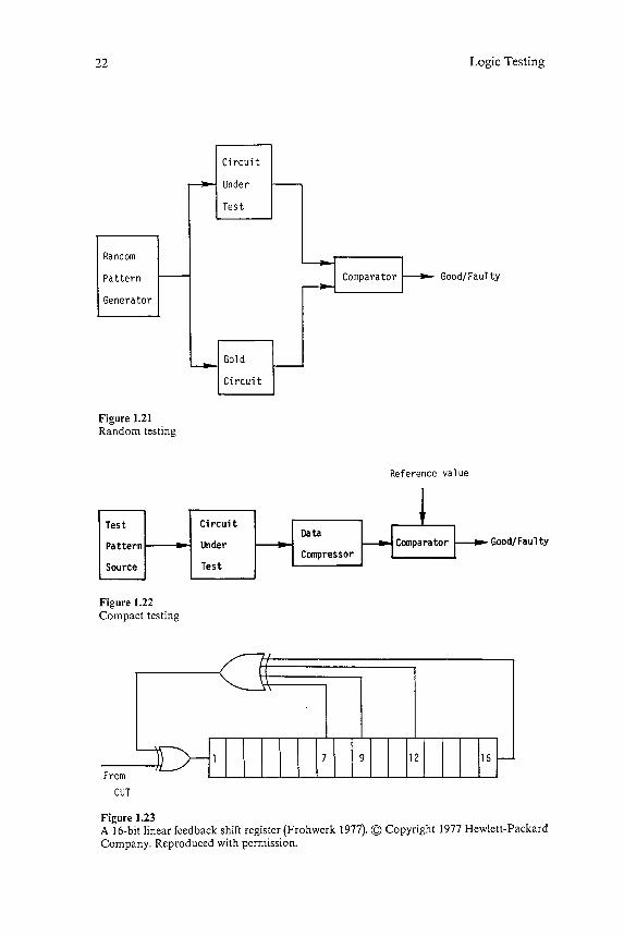
test patterns and correct responses are generated in advance and stored inmemory . Test patterns are produced either manually , by a design or testengineer, or automatically , by test-generation programs . In contrast , bothtest patterns and reference values can be produced each time a CUT istested by hardware -implemented algorithms . In these hardware -basedschemes, test patterns are usually generated randomly or pseudorandomlyand simultaneously applied to the CUT and a known good circuit , called agold circuit . The output responses of the CUT are then compared with those
of the gold circuit. This type of testing method (figure 1.21) is called randomtesting, and in contrast the former software -based testing is called deterministic
testing. Deterministic testing requires costly or time -consuming testgeneration and memory to store huge amounts of test data , where asrandom testing eliminates the cost and the time requirement of generatingor storing test data . However , random testing has disadvantages : The need
for a gold circuit may be bothersome , and the reliability of the gold circuit isnot guaranteed . Synchronization of the two circuits and fault coverage ofrandom test patterns may also cause problems .
In the above-mentioned testing schemes, the total responses are com-
Test CircuitPattern Under Good/FaultySource Test
.22
Figure 1.23A 16-bit linear feedback shift register (Frohwerk 1977). ~ Copyright 1977 Hewlctt-PackardCompany. Reproduced with permission.
Logic Testing22
Circuit
Under
Test
Random
Pattern Comparator Good/ Faulty
Generator
Gold
Circuit
Figure 1.21Random testing
Reference value
Figure 1
1 7 9 12 16
From
CUT
Compact testing
Test CircuitData
Pattern Under ~ Comparator Good/ FaultyCompressor
Source Test
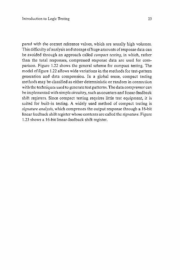
Introduction to Logic Testing 23
pared with the correct reference values, which are usually high volumes .This difficulty of analysis and storage of huge amounts of response data canbe avoided through an approach called compact testing, in which , rather
than the total responses, compressed response data are used for comparison. Figure 1.22 shows the general scheme for compact testing . The
model of figure 1.22 allows wide variations in the methods for test-patterngeneration and data compression . In a global sense, compact testingmethods may be classified as either deterministic or random in connection
with the techniques used to generate test patterns . The data compressor canbe implemented with simple circuitry , such as counters and linear -feedback
shift registers. Since compact testing requires little test equipment , it issuited for built -in testing . A widely used method of compact testing issignature analysis, which compress es the output response through a 16-bitlinear feedback shift register whose contents are called the signature . Figure1.23 shows a 16-bit linear -feedback shift register .