Introduction Technical Note - micron.com
16
Technical Note Uprating Semiconductors for High-Temperature Applications Introduction Uprating is used to evaluate a semiconductor component's ability to function and per- form when used outside of the manufacturer’s specified temperature range 21 . Before operating a DRAM component above its maximum specified temperature, a cus- tomer can use the uprating process to determine the related risks. Uprating is possible because semiconductor manufacturers design margin into their products to increase device yield and reliability. Through its commercial off-the-shelf (COTS) program, the U.S. Department of Defense has been uprating for a number of years. Three major con- cerns are associated with uprating: • Device functionality and performance to data sheet specifications • Device reliability • Package reliability This technical note describes the issues associated with temperature uprating and the risks involved in using components outside the manufacturers’ environmental specifi- cations. It focuses specifically on temperature uprating and the significant failure mechanisms associated with operating semiconductors outside their specified temper- ature ranges. The failure mechanisms apply to all semiconductor products, whether manufactured by Micron or any other semiconductor company. TN-00-18: Temperature Uprating on Semiconductors Introduction PDF: 09005aef81694133/Source: 09005aef8169415f tn0018.pdf - Rev. G 2/2020 EN 1 Micron Technology, Inc. reserves the right to change products or specifications without notice. © 2004 Micron Technology, Inc. All rights reserved. Products and specifications discussed herein are subject to change by Micron without notice.
Transcript of Introduction Technical Note - micron.com

Technical NoteUprating Semiconductors for High-Temperature Applications
IntroductionUprating is used to evaluate a semiconductor component's ability to function and per-form when used outside of the manufacturer’s specified temperature range21.
Before operating a DRAM component above its maximum specified temperature, a cus-tomer can use the uprating process to determine the related risks. Uprating is possiblebecause semiconductor manufacturers design margin into their products to increasedevice yield and reliability. Through its commercial off-the-shelf (COTS) program, theU.S. Department of Defense has been uprating for a number of years. Three major con-cerns are associated with uprating:
• Device functionality and performance to data sheet specifications• Device reliability• Package reliability
This technical note describes the issues associated with temperature uprating and therisks involved in using components outside the manufacturers’ environmental specifi-cations. It focuses specifically on temperature uprating and the significant failuremechanisms associated with operating semiconductors outside their specified temper-ature ranges. The failure mechanisms apply to all semiconductor products, whethermanufactured by Micron or any other semiconductor company.
TN-00-18: Temperature Uprating on SemiconductorsIntroduction
PDF: 09005aef81694133/Source: 09005aef8169415ftn0018.pdf - Rev. G 2/2020 EN 1 Micron Technology, Inc. reserves the right to change products or specifications without notice.
© 2004 Micron Technology, Inc. All rights reserved.
Products and specifications discussed herein are subject to change by Micron without notice.
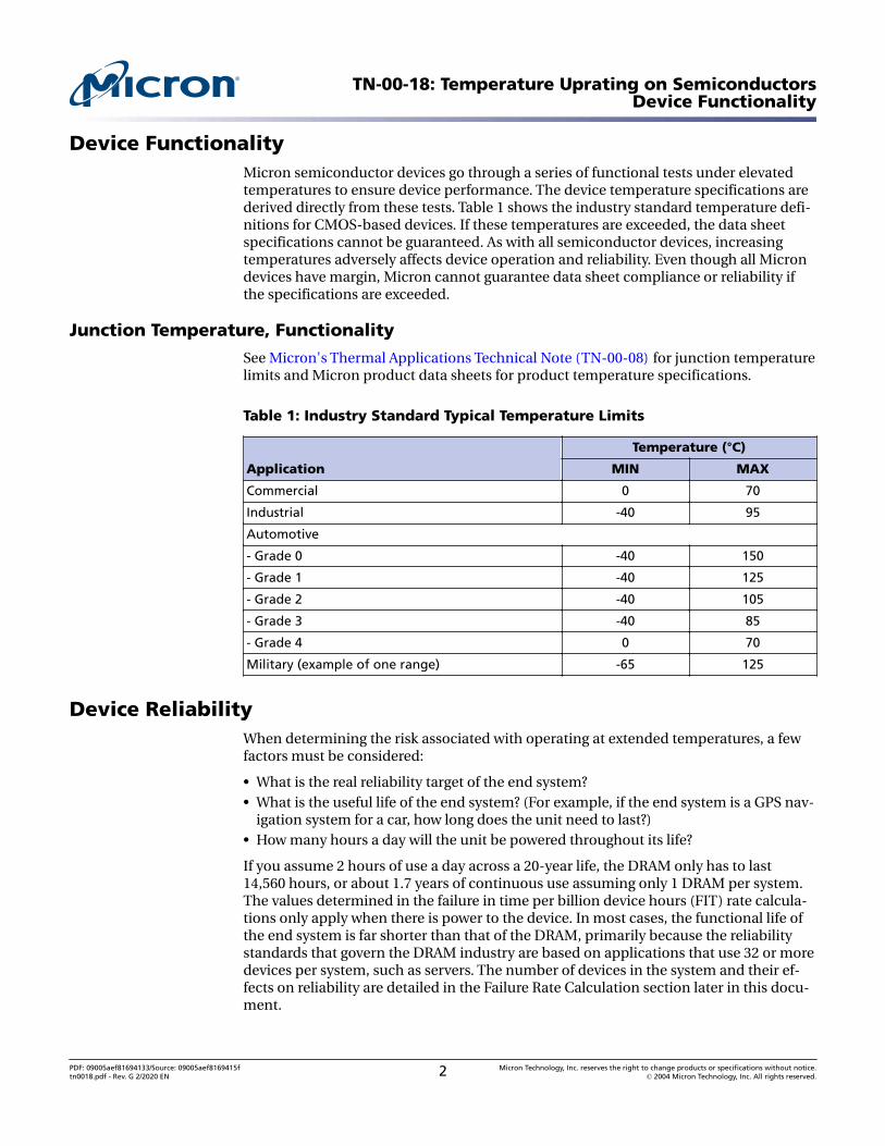
Device FunctionalityMicron semiconductor devices go through a series of functional tests under elevatedtemperatures to ensure device performance. The device temperature specifications arederived directly from these tests. Table 1 shows the industry standard temperature defi-nitions for CMOS-based devices. If these temperatures are exceeded, the data sheetspecifications cannot be guaranteed. As with all semiconductor devices, increasingtemperatures adversely affects device operation and reliability. Even though all Microndevices have margin, Micron cannot guarantee data sheet compliance or reliability ifthe specifications are exceeded.
Junction Temperature, Functionality
See Micron's Thermal Applications Technical Note (TN-00-08) for junction temperaturelimits and Micron product data sheets for product temperature specifications.
Table 1: Industry Standard Typical Temperature Limits
Application
Temperature (°C)
MIN MAX
Commercial 0 70
Industrial -40 95
Automotive
- Grade 0 -40 150
- Grade 1 -40 125
- Grade 2 -40 105
- Grade 3 -40 85
- Grade 4 0 70
Military (example of one range) -65 125
Device ReliabilityWhen determining the risk associated with operating at extended temperatures, a fewfactors must be considered:
• What is the real reliability target of the end system?• What is the useful life of the end system? (For example, if the end system is a GPS nav-
igation system for a car, how long does the unit need to last?)• How many hours a day will the unit be powered throughout its life?
If you assume 2 hours of use a day across a 20-year life, the DRAM only has to last14,560 hours, or about 1.7 years of continuous use assuming only 1 DRAM per system.The values determined in the failure in time per billion device hours (FIT) rate calcula-tions only apply when there is power to the device. In most cases, the functional life ofthe end system is far shorter than that of the DRAM, primarily because the reliabilitystandards that govern the DRAM industry are based on applications that use 32 or moredevices per system, such as servers. The number of devices in the system and their ef-fects on reliability are detailed in the Failure Rate Calculation section later in this docu-ment.
TN-00-18: Temperature Uprating on SemiconductorsDevice Functionality
PDF: 09005aef81694133/Source: 09005aef8169415ftn0018.pdf - Rev. G 2/2020 EN 2 Micron Technology, Inc. reserves the right to change products or specifications without notice.
© 2004 Micron Technology, Inc. All rights reserved.

The long-term reliability and failure rates for CMOS devices is typically described in theform of a curve depicting the life of the IC. This reliability curve is known as a bathtubcurve due to its shape (see the figure below). The curve shows the failure rate of a popu-lation of ICs over time. A small percentage of devices will have inherent manufacturingdefects after the devices have passed all electrical testing and are functional at time = 0.Manufacturing defects caused by contamination and process variation lead to a shorterlife in comparison to the remaining population. These defects are referred to as “infantmortality.” Infant mortality makes up only a small percentage of the total population,but is the largest percentage of early life failures in ICs.
Figure 1: Reliability Curve
Useful life
Time
Hazard Rateh(t)
Infantmortality
Wearout
Mean time between failures (MTBG)applies in this range
Random failures
DRAM devices are subjected to 125°C at elevated voltages (burn-in) to remove the in-fant mortality part of the population prior to shipping. After the devices in the infantmortality section of the bathtub curve are removed from the population, the remainingpart of the population displays a stable field failure rate. Micron uses an intelligent bur-nin — the parts are operated during the stress condition to show the exact time of fail-ure. Following the infant mortality section, there is a relatively flat portion of the bath-tub curve that represents the useful life of the IC, where you would expect to see a verylow field failure rate. The random field failures experienced during the useful life of theIC will eventually be replaced with an exponential failure rate. This is shown in the wearout section of the bathtub curve. The time frame and random field failures in the usefullife of the IC can be predicted using statistics based on lab data from a sample of partsand will vary greatly depending on the operating temperature the IC. This process is ex-plained in detail in the following pages.
TN-00-18: Temperature Uprating on SemiconductorsDevice Reliability
PDF: 09005aef81694133/Source: 09005aef8169415ftn0018.pdf - Rev. G 2/2020 EN 3 Micron Technology, Inc. reserves the right to change products or specifications without notice.
© 2004 Micron Technology, Inc. All rights reserved.
Long-Term ReliabilityStatistically predicting the long-term reliability of a DRAM requires test conditions thataccelerate the stress on the device to screen out those with defects, while at the sametime not damaging the remaining portion of the population. Both temperature andvoltage are used as acceleration factors during testing. Accelerated temperature andvoltages are not set to a point that would damage the device, thereby causing a failurethat would not occur under normal operating conditions. During high temperature op-erating life testing, the devices are subjected to 125°C at an internal voltage of VCC +0.4V. Afterward, extrapolation from accelerated conditions to nominal conditions ispossible.
Temperature Acceleration Factor
The Arrhenius equation, shown below, is used to statistically predict and model the ac-celerations factor due to temperature.
Arrhenius Equation
= Boltzmann’s constant = 8.617 x 10⁻⁵ eV/K= Operating temperature in kelvins= Stress temperature in kelvins= Activation energy for respective failure mechanism
kTO
TS
EA
AFT = e
EAk
1 1TO TS
The stress temperature (TS) used to collect data is 125°C. TO is the normalized operatingtemperature. All temperature data is converted into degrees kelvin. Boltzmann’s con-stant, illustrated as k in the Arrhenius equation, is equal to 8.617 × 10⁻⁵eV/K. The activa-tion energy (EA), expressed in electron volts (eV), is a function of the temperature de-pendence on the failure mechanism. The lower the EA, the less influence the tempera-ture has on the failure mechanism. EA is derived through experimental stress data col-lected at burn-in over time that is common among all semiconductor devices. In thecase of DRAM, the most relevant activation energy is due to the time-dependent dielec-tric breakdown (TDDB). When TO is equal to TS, the acceleration factor due to tempera-ture is equal to 1. As seen by the Arrhenius equation, temperature has an exponentialeffect on the long-term reliability of all CMOS-based ICs.
Voltage Acceleration Factor
The second acceleration factor used in long-term reliability testing is voltage. The volt-age acceleration factor is shown below. Voltage stress is independent of the operatingvoltage specified in the data sheet in most cases. Most DRAM devices internally regulatethe voltage down to an internal operating voltage, VCC, of the given process. During thehigh-temperature operating life test and burn-in, the regulators are disabled with thevoltage moved to VCC + 0.4V as a stress voltage. The constant (β) is determined experi-mentally in relation to TDDB, representing the slope in relation to the time between a
TN-00-18: Temperature Uprating on SemiconductorsLong-Term Reliability
PDF: 09005aef81694133/Source: 09005aef8169415ftn0018.pdf - Rev. G 2/2020 EN 4 Micron Technology, Inc. reserves the right to change products or specifications without notice.
© 2004 Micron Technology, Inc. All rights reserved.

failure versus the stress voltage. β is primarily dependent on the thickness of the gateoxide used in the manufacturing process. As shown by this model, voltage is also expo-nentially related to the reliability of CMOS devices.
Voltage Acceleration Factor
βVS
VO
= Constant, the value is derived experimentally= Stress voltage= Operating voltage
AFV = eβ(Vs - Vo)
Overall Acceleration Factor
The overall acceleration factor (AFOA, shown below) is calculated as the product of thetwo respective acceleration factors (temperature and voltage). The AFOA shows the rela-tionship from the stress conditions using unregulated voltages to nominal conditions asseen in the system.
Overall Acceleration Factor
AFOA = AFV x AFT
TN-00-18: Temperature Uprating on SemiconductorsLong-Term Reliability
PDF: 09005aef81694133/Source: 09005aef8169415ftn0018.pdf - Rev. G 2/2020 EN 5 Micron Technology, Inc. reserves the right to change products or specifications without notice.
© 2004 Micron Technology, Inc. All rights reserved.

Failure Rate CalculationThe failure rate of an IC can be expressed in many different ways, but once you have thedata, it is not difficult to convert the data into the desired format. Assuming that failuresoccur as random independent events, component failure rates can be calculated usingthe equation below. The three components used to predict the final failure rate are Pois-son statistic, device hours tested, and the number of failures in the sample size beingtested.
Failure Rate Calculation
Failurerate
PnDevice hours at
accelerated environmentrelative to systemoperating conditions
AFOA x
=
The Poisson statistic used in this equation, Pn, is derived from the Poisson probabilitydistribution equation shown in the figure below (Poisson Probability Distribution Equa-tion). Pr in the equation represents 1 minus the confidence level at which the failurerate is calculated. In the equation, r represents the total number of fails in the samplesize. After Pr and r are defined, you can solve for Pn.
Calculating the Poisson statistic can be difficult without a statistics calculator, but thevalues used in the Poisson curves can be estimated, as seen in Figure 2. C represents thenumber of fails in the sample size, and Pa represents 1 minus the confidence level.Drawing a horizontal line from the Pa value until it intersects the curve, C, equals thePoisson statistic. The Pn value can then be determined by dropping a vertical line downfrom the intersection. The confidence levels of 60% and 90% are shown based on zerofails in the sample size.
Table 2 shows the Poisson statistic based on the number of fails versus the confidencelevels set at 60% and 90% from 0 to 5 failures. Micron uses a 60% confidence level for allfailure rate calculations published for DRAM devices. If a higher level of confidence isneeded, recalculating this can be done using a different Pn to represent the desired con-fidence level.
Poisson Probability Distribution Equation
= One minus the confidence level at which the failure rate is calculated= The total number of failed devices from our test samples
Pr
r
Pr = Ʃi = 0
r(e
(i!)
)PnPnr
TN-00-18: Temperature Uprating on SemiconductorsFailure Rate Calculation
PDF: 09005aef81694133/Source: 09005aef8169415ftn0018.pdf - Rev. G 2/2020 EN 6 Micron Technology, Inc. reserves the right to change products or specifications without notice.
© 2004 Micron Technology, Inc. All rights reserved.

Figure 2: Poisson Curves
Note: 1. C = Acceptable number of failures in the sample.
Table 2: Poisson Statistic
Number of Fails 60% Confidence Level 90% Confidence Level
0 0.916 2.303
1 2.022 3.890
2 3.105 5.322
3 4.175 6.681
4 5.237 7.994
5 6.291 9.275
The total device hours tested under the stress conditions is relatively straightforward.For this part of the equation, the total number of devices is multiplied by the totalamount of time in the high temperature operating test. The total number of fails obvi-ously affects the final reliability calculation, but so does the time of the fail. Early fail-ures have a greater effect on the final result than do fails later in the test flow. This isbecause early failures reduce the total number of device test hours more than failuresthat happen later in the test flow. For example, if the sample size is 100 throughout thetesting and each device is tested for 1008 hours, the total device hours equates to 100 ×1008 or 100,800 hours of device operation.
The final element of the failure rate calculation is the overall acceleration facture due totemperature and voltage as discussed earlier. This acceleration factor is where the tem-
TN-00-18: Temperature Uprating on SemiconductorsFailure Rate Calculation
PDF: 09005aef81694133/Source: 09005aef8169415ftn0018.pdf - Rev. G 2/2020 EN 7 Micron Technology, Inc. reserves the right to change products or specifications without notice.
© 2004 Micron Technology, Inc. All rights reserved.
perature can be varied to determine the failure rate based on a nominal voltage andtemperature.
After the failure rate is calculated, it can be expressed in two formats: failures per billiondevice hours (FIT) or the percentage of failures per thousand device hours. To convertthe failure rate calculation into a FIT rate, the value needs to be multiplied by 10+9, andto convert this into a percent failures per thousand device hours, the value is multipliedby 10+5. The failure rate at Micron is expressed in failures per billion device hours, FIT.
To determine the total system FIT rate, the calculated FIT rate for a given IC is multi-plied by the number of DRAM devices in the system. For example, if the FIT rate for asingle component is 10, a system using 4 DRAM devices would have a total system FITrate of 40 FIT. As mentioned earlier, this is the reason that the number of DRAM used inthe system is crucial to overall system reliability.
TN-00-18: Temperature Uprating on SemiconductorsFailure Rate Calculation
PDF: 09005aef81694133/Source: 09005aef8169415ftn0018.pdf - Rev. G 2/2020 EN 8 Micron Technology, Inc. reserves the right to change products or specifications without notice.
© 2004 Micron Technology, Inc. All rights reserved.
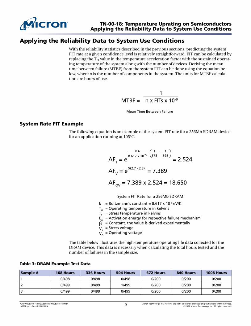
Applying the Reliability Data to System Use ConditionsWith the reliability statistics described in the previous sections, predicting the systemFIT rate at a given confidence level is relatively straightforward. FIT can be calculated byreplacing the TO value in the temperature acceleration factor with the sustained operat-ing temperature of the system along with the number of devices. Deriving the meantime between failure (MTBF) from the system FIT can be done using the equation be-low, where n is the number of components in the system. The units for MTBF calcula-tion are hours of use.
Mean Time Between Failure
MTBF = n x FITs x 10-9
1
System Rate FIT Example
The following equation is an example of the system FIT rate for a 256Mb SDRAM devicefor an application running at 105°C.
System FIT Rate for a 256Mb SDRAM
βVS
VO
= Boltzmann’s constant = 8.617 x 10⁻⁵ eV/K= Operating temperature in kelvins= Stress temperature in kelvins= Activation energy for respective failure mechanism= Constant, the value is derived experimentally= Stress voltage= Operating voltage
kTO
TS
EA
AFT = e = 2.524
= 7.389AFV = e
AFOV = 7.389 x 2.524 = 18.650
8.617 x 10⁻⁵
5(2.7 - 2.3)
0.6 1378
1398
The table below illustrates the high-temperature operating life data collected for theDRAM device. This data is necessary when calculating the total hours tested and thenumber of failures in the sample size.
Table 3: DRAM Example Test Data
Sample # 168 Hours 336 Hours 504 Hours 672 Hours 840 Hours 1008 Hours
1 0/498 0/498 0/498 0/200 0/200 0/200
2 0/499 0/499 1/499 0/200 0/200 0/200
3 0/499 0/499 0/499 0/200 0/200 0/200
TN-00-18: Temperature Uprating on SemiconductorsApplying the Reliability Data to System Use Conditions
PDF: 09005aef81694133/Source: 09005aef8169415ftn0018.pdf - Rev. G 2/2020 EN 9 Micron Technology, Inc. reserves the right to change products or specifications without notice.
© 2004 Micron Technology, Inc. All rights reserved.

Table 3: DRAM Example Test Data (Continued)
Sample # 168 Hours 336 Hours 504 Hours 672 Hours 840 Hours 1008 Hours
Total 0/1496 0/1496 1/1496 0/0600 0/0600 0/0600
Failure Analysis Summary
Interval Sample # No. of Fails
504 hours 2 1
The device hours is a simple calculation of the number of devices multiplied by the totalnumber of hours tested, measured in hours:
Device hours = (1496 - 168) + (1496 - 168) + (1496 - 168) + (600 - 168) + (600 - 168) + (600- 168) = 1,056,384 or 1.056 × 10+6
The Poisson statistic is calculated using a single fail in the sample size at a 60% confi-dence level, as shown below.
Posson Statistic Calculated at a 60% Confidence Level
0.4 =
P(n) = 2.022
Ʃi = 0
1(e
(i!)
)PnPn1-
The final failure rate and FIT can now be calculated for the operating temperature of105°C.
Final Failure and FIT Rates
FR = failure rate
FR =
FR = 1.027 x 10⁻⁷
FR = 1.027 x 10-7 x 1.0 x 109 = 102
2.0221.056 x 106 x 18.650
With the FIT rate calculated, the MTBF can be calculated. In the figure below, we areassuming one device in the system (see Figure 3).
TN-00-18: Temperature Uprating on SemiconductorsApplying the Reliability Data to System Use Conditions
PDF: 09005aef81694133/Source: 09005aef8169415ftn0018.pdf - Rev. G 2/2020 EN 10 Micron Technology, Inc. reserves the right to change products or specifications without notice.
© 2004 Micron Technology, Inc. All rights reserved.

Mean Time Between Failure Calculation
MTBF =
MTBF ~ 9.8 million hours
MTBF ~ 1100 years
1 x 102 x 10-9
1
~
~
Figure 3: Example of Memory System Mean Time Between Failure for Multiple Micron DRAM Com-ponents
TN-00-18: Temperature Uprating on SemiconductorsApplying the Reliability Data to System Use Conditions
PDF: 09005aef81694133/Source: 09005aef8169415ftn0018.pdf - Rev. G 2/2020 EN 11 Micron Technology, Inc. reserves the right to change products or specifications without notice.
© 2004 Micron Technology, Inc. All rights reserved.

Package ReliabilityPackage reliability is generally not a concern at constant operating temperatures below125°C. However, reliability predictions can be made if conditions in the use environ-ment are known and acceleration factors are calculated. Data provided by Micron in de-vice qualification reports or acquired by applying knowledge of expected failure mecha-nisms in the use environment can be used to calculate the acceleration factors.
The Hallberg-Peck acceleration model is commonly used for temperature and humiditystress.
Hallberg-Peck
= Activation energy of defect mechanism (0.9 commonly used)
= Stress test environment relative humidity= Operating use environment relative humidity= Stress test environment temperature= Operating use environment temperature
EA
RHS
RHOTS
TO
Boltzmann’s constant (k) = 8.617 x 10⁻⁵ eV/K
AF = x e xRHs
RHO
EA
k
31TS
1TO
where:
Two common acceleration models are used to calculate thermal cycling stress:
Coffin-Manson
AF =mTS
TO
ΔΔ
Modified Coffin-Manson (SnPb Solder Joints)
where:= Exponent dependent on defect mechanism and material= Stress test thermal cycle temperature change= Operating use thermal cycle temperature change= Operating use thermal cycling frequency= Stress test thermal cycling frequency= Maximum temperature during stress test thermal cycle= Maximum temperature during operating use thermal cycle
mTS
TO
FO
FS
TS
TO
AF = x x e1.9 1/3TS FO [0.01 x ( - )]TS TO
FSTO
ΔΔ
ΔΔ
~
TN-00-18: Temperature Uprating on SemiconductorsPackage Reliability
PDF: 09005aef81694133/Source: 09005aef8169415ftn0018.pdf - Rev. G 2/2020 EN 12 Micron Technology, Inc. reserves the right to change products or specifications without notice.
© 2004 Micron Technology, Inc. All rights reserved.

SummaryWhen exceeding the specified device temperature limits, a customer faces three con-cerns. First, the functionality and performance of the device must be considered, andthe system design must be adjusted accordingly. Second, device reliability is reduced,which can be calculated using the proper reliability equations. Finally, temperatures be-low +125°C are not a concern for package reliability, but temperature cycling can be aconcern and should be avoided.
Uprating can be performed on many levels. For instance, the military—through itsCOTS program—buys commercially rated semiconductors and re-evaluates device suit-ability for its temperature-rated applications. This can be accomplished using a varietyof methods, including common practices of parameter conformance, parameter re-characterization, stress balancing, and higher assembly level testing13. However, theseprocesses are very expensive and add to the cost of the components18. At the other ex-treme, a user could simply take commercially rated devices, assess their critical func-tion parameters and decreased reliability, and simply design the system around theseissues.
Many semiconductor manufacturers design significant margin into their products.However, semiconductor manufacturers who provide products for multiple tempera-ture specification ranges, as Micron does, generally do not have different device fabrica-tion processes based on the expected temperature range of the application. For exam-ple, commercial and industrial devices are generally from the same fabrication processand, therefore, have equivalent intrinsic device reliability. The primary difference is thatthe industrial devices have been screened for data sheet functionality at the necessarytemperature extremes13.
Before products are uprated, a thorough understanding of the thermal environment isneeded. Uprating can be an expensive process. If devices are never subjected to exten-ded temperatures, there is probably no reason to add the costs associated with uprat-ing, even if the system has been specified to extended temperatures. For details on ther-mal measurements, see Micron’s Thermal Application Technical Note (TN-00-08).
TN-00-18: Temperature Uprating on SemiconductorsSummary
PDF: 09005aef81694133/Source: 09005aef8169415ftn0018.pdf - Rev. G 2/2020 EN 13 Micron Technology, Inc. reserves the right to change products or specifications without notice.
© 2004 Micron Technology, Inc. All rights reserved.
References
Book References
1. Harman, G. and Harper, C.A., Wire Bonding in Microelectronics Materials, Processes, Reli-ability, and Yield, 2nd Ed., McGraw-Hill, New York, 1997.
2. Kirschman, R., High-Temperature Electronics, IEEE Press, New York, 1999.
3. Lall, P., Precht, M. G., and Hakim, E. B., Influence of Temperature on Microelectronics,CRC Press, Boca Raton, 1997.
4. McCluskey F. P., Grzybowski, R., and Podlesak, T., High-Temperature Electronics, CRCPress, Boca Raton, 1997.
5. Amerasekera, E. Ajith, Najm, Farid N., Failure Mechanisms in Semiconductor Devices, 2ndEd., John Wiley & Sons, Hoboken, 1998.
Paper References
6. Barker, D., “Ruggedizing Laptop Computers for Mobile Applications.” Presented at thefirst workshop on use of components outside specified temperature limits, CALCE EPRC,University of Maryland, College Park, January 23, 1997.
7. Biddle, S., “Beyond Quality – Assuring the Reliability of Plastic Encapsulated IntegratedCircuits,” COTS Journal, March 2003.
8. Condra, L., Das, D., Pendse, N., and Pecht, M., “Junction Temperature Considerations inEvaluating Electronic Parts for Use Outside Manufacturers-Specified Temperature Rang-es,” IEEE Trans. Comp. Pack. Tech., Vol. 24, pp. 721–728, December 2001.
9. Das, D., Pendse, N., Pecht, M., and Wilkinson, C., “Deciphering the Deluge of Data,” Cir-cuits and Devices, September 2000.
10. Das, D., Pendse, N., Pecht, M., and Wilkinson, C., “Parameter Recharacterization: AMethod of Thermal Uprating,” IEEE Trans., Comp. Pack. Tech., Vol. 24, pp. 729–737, De-cember 2001.
11. Dasgupta, A., et al., “Does the Cooling of Electronics Increase Reliability?” Presented atthe Proc. Thermal Stresses '95 Conference, No. 231, 1995.
12. Davila-Rieth, K., “Uprating Assemblies for Military Computer Systems,” Presented at thefirst workshop on use of components outside specified temperature limits, CALCE EPRC,University of Maryland, College Park, January 23, 1997.
13. Humphrey, D., et al., “An Avionics Guide to Uprating of Electronic Parts,” IEEE Trans.Comp. Pack. Tech., Vol. 23, pp. 595–599, September 2000.
14. Kroger, R., “Manufacturer Part Assessment: A Pragmatic Approach,” Presented at thefirst workshop on use of components outside specified temperature limits, CALCE EPRC,University of Maryland, College Park, January 23, 1997.
15. Lall, P., et al., “Characterization of Functional Relationship Between Temperature andMicroelectronic Reliability,” Microelecton, Vol. 35, No. 3, pp. 377–402, March 1995.
16. McCluskey, P., et al., “Uprating of Commercial Parts for Use in Harsh Environments,”CALCE EPRC Rep., November 1996.
17. Ng, K. K., “A Survey of Semiconductor Devices,” IEEE Trans. Electron Devices, Vol. 43, pp.1760–1766, October 1996.
18. Pecht, M., “Issues Affecting Early Affordable Access to Leading Electronics Technologiesby the U.S. Military and Government,” Circuit World, Vol. 22, No. 2, pp. 7–15, 1996.
TN-00-18: Temperature Uprating on SemiconductorsReferences
PDF: 09005aef81694133/Source: 09005aef8169415ftn0018.pdf - Rev. G 2/2020 EN 14 Micron Technology, Inc. reserves the right to change products or specifications without notice.
© 2004 Micron Technology, Inc. All rights reserved.

19. Pendse, N., Thomas, D., Das, D., and Precht, M., “Uprating of a Single Inline MemoryModule,” IEEE Trans. Comp. Pack. Tech, Vol. 25, No. 2, pp. 266–269, June 2002.
20. Suhir, E., “Accelerated Life Testing (ALT) in Microelectronics and Photonics: Its Role, At-tributes, Challenges, Pitfalls, and Interaction With Qualification Tests,” Journal of Elec-tronic Packaging, Vol.124, pp. 281–290, September 2002.
21. Wright, M., et al., “Uprating Electronic Components for use Outside their TemperatureSpecification Limits,” IEEE Trans. Comp., Packaging, and Manufacturing Technology-PartA, Vol. 20, pp. 252–256, June 1997.
Micron References
22. Quality and Reliability Handbook.
23. 256Mb Qualification Document.
24. A. Gallo, Fink, J., “Reliability of Commercial Plastic Encapsulated Microelectronics atTemperatures from +125°C to +300°C,” Dexter Technical Paper, July 1999.
TN-00-18: Temperature Uprating on SemiconductorsReferences
PDF: 09005aef81694133/Source: 09005aef8169415ftn0018.pdf - Rev. G 2/2020 EN 15 Micron Technology, Inc. reserves the right to change products or specifications without notice.
© 2004 Micron Technology, Inc. All rights reserved.

Revision History
Rev. G – 2/2020
• Updated Introduction, Device Functionality, and Failure Rate Calculation sections.• Updated template.
Rev. F – 5/10
• Updated Table 1, "Junction Temperature, Functionality," on page 2.
Rev. E – 5/08
• Updated Table 1, "Junction Temperature, Functionality," on page 2.
Rev. D – 1/07
• Updated Table 1, "Junction Temperature, Functionality," on page 2.• Edited for readability.• Corrected Table 2, "Industry-Standard Typical Junction Temperature Limits", on page
2, Under the hood temperature to -40-150.
Rev. C – 11/06
• Updated "Device Reliability" section• Added "Long-Term Reliability", "Temperature Acceleration Factor", "Overall Accelera-
tion Factor", "Failure Rate Calculation", and "Applying the Reliability Data to SystemUse Conditions" sections.
Rev. B – 11/05
• Updated template.• Corrected typos: Equation 2 on page 2, TN-00-08 reference on page 10, and Boltz-
mann's constant from 8.6171 to 8.6174 on page 10.
Rev. A – 10/04
• Initial release
8000 S. Federal Way, P.O. Box 6, Boise, ID 83707-0006, Tel: 208-368-4000www.micron.com/products/support Sales inquiries: 800-932-4992
Micron and the Micron logo are trademarks of Micron Technology, Inc.All other trademarks are the property of their respective owners.
This data sheet contains minimum and maximum limits specified over the power supply and temperature range set forth herein.Although considered final, these specifications are subject to change, as further product development and data characterization some-
times occur.
TN-00-18: Temperature Uprating on SemiconductorsRevision History
PDF: 09005aef81694133/Source: 09005aef8169415ftn0018.pdf - Rev. G 2/2020 EN 16 Micron Technology, Inc. reserves the right to change products or specifications without notice.
© 2004 Micron Technology, Inc. All rights reserved.