Introduction on NBTI - WebHome -...
14
Introduction on NBTI Prepared by : Chan Tuck Boon 1 10/9/2010
Transcript of Introduction on NBTI - WebHome -...

Introduction on NBTI
Prepared by : Chan Tuck Boon1
10/9/2010

NanoCAD Lab
What is NBTI ?
• NBTI : Negative Bias Temperature Instability
• Vth varies on PMOS device
– Vth increase with negative bias, Vgs=-Vdd
– But recover with zero bias , Vgs=0
2
Source : Vincent Huard, IEDM 2007
Vth increased

NanoCAD Lab
NBTI impact
• Wang, VLSI 2010
• 7% to10% frequency degradation on benchmark circuits
• Mangalagiri, ICCAD 2008
– 5% to 10% delay degradation in FPGA due to NBTI (PTM model)
– 1% delay degradation for process with hi-Vt and thick oxide.
• Neeraj, IEDM 2005
– Degradation depends on configuration and application.
– Verror > 7 mV (maximum allowed error=7.8mV) for a 64 bit DAC.
• J.C. Lin, IEDM 2006
– SRAM read margin decrease as a result of NBTI stress.
– Limit NBTI impact using a less “read margin” dominant design.
3

NanoCAD Lab
Impact on SRAM
• NBTI shows noticeable impact on SRAM yield
• Yield loss is huge considering NBTI + PBTI
4
Drapatz ,Journal Advances in Radio Science, 2009

NanoCAD Lab
NBTI vs PBTI
• trade-off between NBTI/PBTI and metal gate
thickness
5

NanoCAD Lab
Reaction-diffusion model
• Interface traps is generated when device is stressed
(negative bias)
6
Silicon (inv) Gate Oxide Poly
Si-H
Si
H+
+
+
H,H2
H,H2recovery
Stress
X=0X
H,H2
concentrationDiffusion
Si-H

NanoCAD Lab
Differential Equations for NBTI
7
Reaction
Diffusion
Kv is proportional to Temperature2n=1/3 for reaction
dominant by H2
Source : W. Ping et al. DAC 2007
Stress
Recovery
Analytical model
Recovery factor
Related to

NanoCAD Lab
NBTI Characteristics
• NBTI degradation is front-loaded
• Frequency dependent or independent ?
• Vgs dependence
• Vth variation reduction due to NBTI
8

NanoCAD Lab
Front Loaded Degradation
• Degradation rate is steep at the beginning but slows
down rapidly
9
Source : W. Ping et al. DAC 2007

NanoCAD Lab
Frequency independence
• RD model predicts frequency
independence [Alam, IEDM
2003]
• Contradict observations are
found in
10
http://www.iue.tuwien.ac.at/phd/wittmann/node10.html
NanoCAD Lab
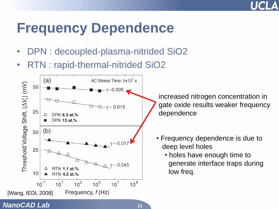
Frequency Dependence
• DPN : decoupled-plasma-nitrided SiO2
• RTN : rapid-thermal-nitrided SiO2
11
[Wang, IEDL 2008]
increased nitrogen concentration in
gate oxide results weaker frequency
dependence
• Frequency dependence is due to
deep level holes
• holes have enough time to
generate interface traps during
low freq.

NanoCAD Lab
NBTI vs Vgs
• ∆Vt increase exponentially with increasing Vgs
12

NanoCAD Lab
NBTI and Vth Variation
13
ΔVth
process
ΔVth NBTIΞ
ΔVth process + ΔVth NBTI
=> Overall process
variation reduced
Source : W. Ping et al. DAC 2007

NanoCAD Lab
On-going Studies on NBTI
• Modeling and characterizing NBTI
– Physical mechanism of NBTI
– Measuring NBTI
– Circuit and architectural level NBTI model
• NBTI mitigation techniques
– Input vector control
• Flipping bit cell data in SRAM
– Power-gating schemes for NBTI
14