Introduction of Company and Products - nogami-gk.co.jp · Nogamigiken Co., Ltd. Manufacturing and...
29
Nogamigiken Co., Ltd. Manufacturing and consulting company specialized in precision stamping Introduction of Company and Products Dies are not just equipment for mass production. They are important tools for earing a profit.
Transcript of Introduction of Company and Products - nogami-gk.co.jp · Nogamigiken Co., Ltd. Manufacturing and...

Nogamigiken Co., Ltd.
Manufacturing and consulting company specialized in precision stamping
Introduction of Company and Products
Dies are not just equipment for mass production. They are important tools for earing a profit.
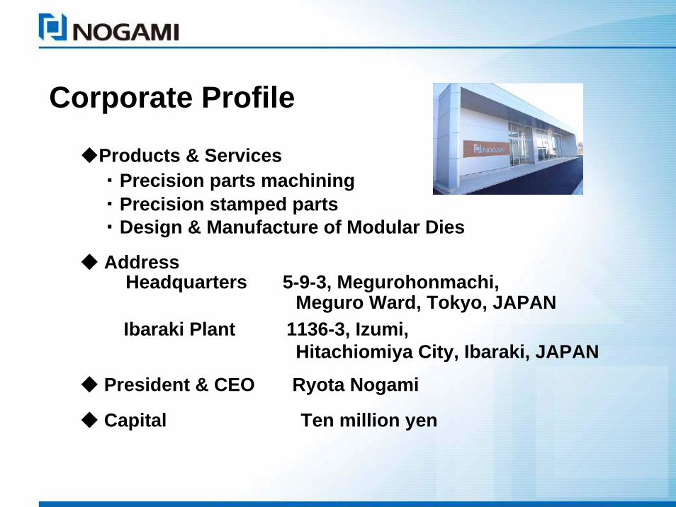
Corporate Profile
◆Products & Services・ Precision parts machining ・ Precision stamped parts・ Design & Manufacture of Modular Dies
◆ AddressHeadquarters 5-9-3, Megurohonmachi,
Meguro Ward, Tokyo, JAPANIbaraki Plant 1136-3, Izumi,
Hitachiomiya City, Ibaraki, JAPAN
◆ President & CEO Ryota Nogami
◆ Capital Ten million yen

We are devoted to doing our business of MONODZUKURI with a great determination and
good faith, creating valuable products and services, and making a contribution to society.
Be a company capable to deliver solutions.With the aim of becoming the highest quality
MONODZUKURI company in the world.
MONODZUKURI: An art of making goodsMONODZUKURI: An art of making goods

1970 NOGAMI SEIKEN established by Shinryo Nogami
1986 Changed the company name to NOGAMIGIKEN Co., Ltd.
1987 Built Number 1 factory in Ibaraki Prefecture
1990 Started the stamping products & services
1999 Obtained ISO 9000 certification for Ibaraki factories
2001 Started the unitary jigs & services (design & manufacturing in-house)
2011 Registered on the IGES as certificate of Eco Action 21
2013 Built New office building & Unitary-jig factory in Ibaraki Prefecture
ISO 9001
Historical highlights

1. Selected by METI as one of “300 of Japan’s Vibrant Monodzukuri (an art of making goods) Small and Medium Enterprises (SMEs)” May, 2009
2. Adopted by METI as a company to receive a subsidy for product development of Monodzukuri SMEs October, 2009
3. Adopted by JETRO as a company to receive the support service to export hopeful products as exportation July, 2010
4. Adopted by METI as a company to receive a subsidy for SME’s R & D to develop new technology (Developed an innovative stamping die to blank out glass epoxy PCB (FR4)) October, 2010
5. Selected by the Conference for Promotion of Monodzukuri to receive an award of “CHO (SUPER‐)Monodzukuri Innovative Parts and Components”
November, 2011
Awards received by Nogamigiken
METI: Ministry of Economy, Trade and Industry in Japan

NOGAMI has made a study of technology of ultra-precision grinding for over 40 years
The parallelism and perpendicularity tolerance of 0.0005 mm, The most advanced MACHINE existing in the world is incapable of achieving this tolerance.
Core technology~Ultra-precision grinding~

Three kinds of Three kinds of products and products and
services based on services based on our core our core
technology of technology of precise grindingprecise grinding
Precision Parts
Product #1
Precision Parts
Product #1
Products and Services
Precision stamped parts
Product #2
Precision stamped parts
Product #2
Design & Manufacture of Modular DiesProducts #3
Design & Manufacture of Modular DiesProducts #3

NOGAMI has acquired the (technical) know‐how about material selection, heat treatment, shape of cutting‐edge and surface treatment through 41‐year’s experience. Know‐how of keeping the quality and precision solves the problems of early wear and breakage.
Products #1: Precision parts machining~Cutting edge / swaging edge ~

By using the technology achieving ultra‐precision perpendicular and parallelism tolerance, it is capable to stamp out the materials which seems tough to punch; such as thin plate, small pieces, precision parts and materials difficult to stamp
Products #2: Precision stamping/ blankingCapable to stamp out the thin plate, small pieces, precision parts and materials difficult to stamp
Progressive stamping die

Products #2: Precision stamping~Die design~
Composite swaged parts
Brush of micromotor
Composite swaged parts in the die make the cost reducedInvestigating the technologies of die design over 20 years and acquire the know‐how. A parts which consists of 2 components was formerly welded manually, and is swaged in the progressive die. It makes the quality of parts stable and the cost reduced.

〔Laminated parts of motor core 〕Stamp out motor cores and lay ten or so cores, and make them staked at once in
the progressive die
〔Composite parts of miniature vibrating motor and brush 〕Stamp out a brush and stake it with other parts in the progressive die Contact point (thickness: 0.04 mm)
Holder parts (thickness: 0.15 mm)
〔Minute electronic parts 〕Stamp out the parts in complicated form with high precision, high quality &
low cost. You can see how small a parts is as compared with a lead of mechanical pencil
〔Exterior components of stationary 〕Supply fine parts (no scratch, no dent nor burr) stably
Manufacture the parts in a 3‐D form that is high level of difficulty
〔Extremely thin metal parts thickness: minimum 0.005 mm〕
Thickness & Width : 0.08 mm, 80 mm Slit width & length: 0.2 mm & 65 mmStamp with minimum burrs & warp
Products #2: Precision stamping parts

Stamping a thin material as thin as 0.005 mm with
● Prevent contamination and minimize sticking Al on the die. ● Minimize burrs and deformation, and keep the fine section long time
Products #3: Precision Stamping Dies and Jigs ~ Design & Manufacturing ~
≪Aluminum foil ≫0.015 mm
≪TCP Film≫0.12 mm
≪Electrode of Li-ion battery≫0.12 mm
Nogami
Other brand
Thickness

Desire to stamp electrode material minimizing the produceof burrs, deformation and contamination
◇ Precision stamping dieUniform and clean sectionNo projections on the entire edge
Products #3: Precision Stamping Dies and Jigs
◇ Problems associated with Laser machiningProduce of burrs, contamination and projection due to melting active material and base by the heat

Products #3: Precision Stamping Dies and Jigs
Provide a most suitable solution taking in the technology and know‐how of precise manufacturing, cutting edge manufacture and assembly, and the technical skill of design and development to customer
~Ultra precision stamping die~
World’s smallest class Ultra precision stamping die
Stamping die for Lithium‐ion battery with material feeder
Cover R & D to Volume Production

Example of product For R & D
~Handheld punch~ ≪Example of use≫
Checking the punching position, and stamp out World smallest class
Ultra precision stamping die Portable and handy jigs for trial manufacture and R & D
Outstanding sharpness & long lifeHigh stiffness structureLight weight & small sizeMeasures to prevent foreign particles by wear
≪Aluminum foil for electrode thickness: 0.015mm≫
Other brand
Nogamibrand

Most suitable jig for working in a glove box
Ultra‐precision Hand Press for stamping electrodes
Stamped shape & size: Max. 50 mm x 70 mmPunching force: Approximately 200 kgGross weight: Approximately 10 kgSize (W x L x H): 155 x 260 x 315 mm
User‐replaceable dies used for wide variety of products
Example of product for prototyping~Desk-top jig~

Example of Product for Mass production
~ Dies in production line ~【4‐column structure die】 【Double column‐shaped die】
【Stamping die for thermistor】【Die set (Outer guide) structure 】
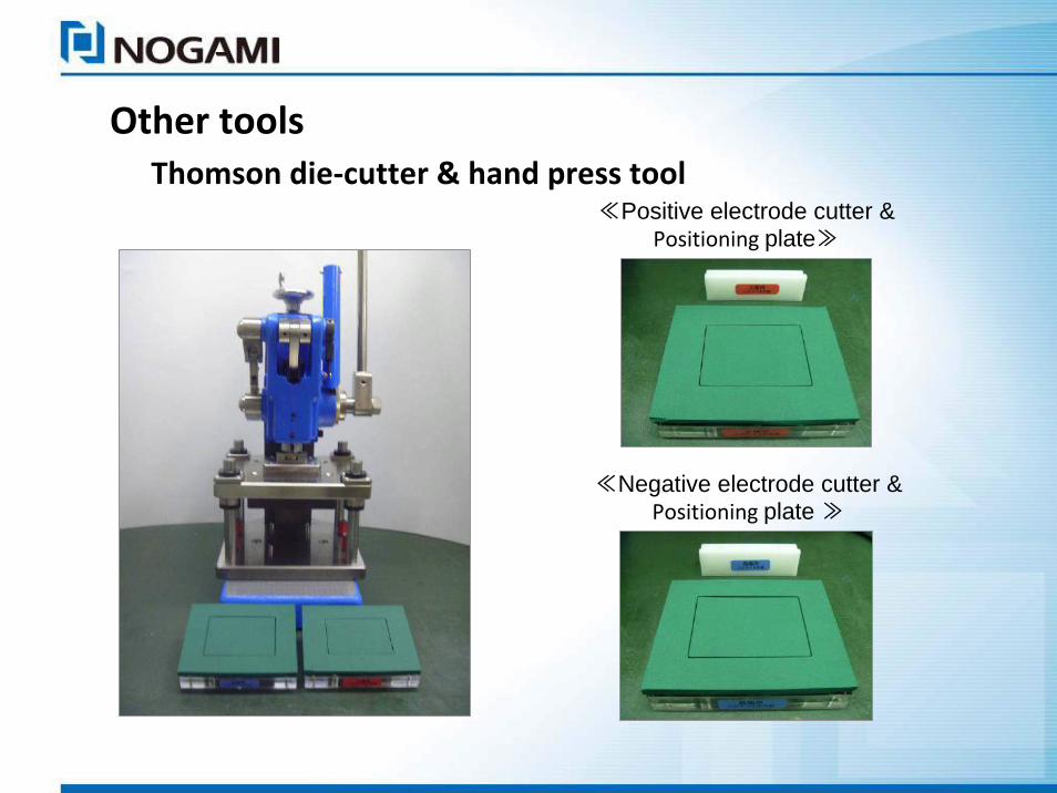
Other toolsThomson die‐cutter & hand press tool
≪Positive electrode cutter & Positioning plate≫
≪Negative electrode cutter & Positioning plate ≫

Accommodating product up to 600 mm wideBest‐suited for prototypingEquipped with a guide and scale
≪Cut surface of positive electrode (Al)≫
Other toolsDesktop ultra‐precision cutting jig
Upper surface Cross section

◇ Points at issue forming the glass epoxy PCB
①Whitening ②Whitening(enlarged) ③Sheared section (enlarged)
Working area Means of forming Point at issue
Area remotely related to the accuracy and quality of product
Blanking with a die Whitening, burrs, crack and scraps are generating
Area intimately related to the accuracy; e.g. the end of the lead
Cutting with a router Cost becomes high due to the low production efficiency
An innovative manufacturing technique to blank out glass epoxy PCB for forming efficiently and
reducing the cost
Whitening
Burr
Whitening
Whitening
Crack
Scrap
A challenge to new engineering development(1)

IssuesContamination
Burrs
Stamping out
electrodes
Maintenance to remove IssuesRegrindingReplacement
A cycle of stamping die
Quality control for mass productionShort life of stamping die causes low productivity
Other brand 10,000-100,000 Shots
Nogami Over 1,000,000 Shots(In case of some customers)
Other brand’s die
Nogami’s die
Die costMaintenance
cost
Labor cost for tooling
changes
Reserved die cost
Loss of materials
Annual cost: 1/31/3
A challenge to new engineering development(2)
Million Yen

Existing NOGAMI
◇ Problem caused by stamping layered collector・Materials were stuck together due to penetration ・ Production line stopped due to short‐life die
Other brand’s die Nogami’s die
A challenge to new engineering development(3)

STEP1Present situation
・Verify the specifications・Conduct a hearing to
grasp the problems
・Make tests using a wide choice of dies・Scientifically verify the test results with analyzers
STEP2Stamping tests
STEP3Test report
STEP4Discussion
・Report test results・Propose the optimum problem-solving
・Confirm customer’s goal through an interview・Discuss an outline of specifications
STEP5Quote & Specifications
・Issue a quotation・Provide drawings & image of product
・Meeting before manufacturing・Manufacture –Trial test・Outgoing inspection
STEP6Manufacture
STEP7Delivery
STEP8Maintenance
・Explain the operation of tool・Hear customer’s questions & advise
・Propose maintenance plan・Dies scheduled maintenance service
Consulting serviceConsulting arrangements

◆ 2,500-power Microscope ◆ High Speed Camera
◆ Energy Dispersive x-ray Spectroscopy (EDS)◆ 300,000-power Scanning Electron Microscope
We observe, analyze and evaluate … on our customer’s behalf.
We attack various problems those have bad influences upon the product quality.
Research & Development structure

Research & Development structure◇ Analysis & measurement laboratory

Research & Development structure◇ Stamping test laboratory
・ Stamping dies & jigs for trial: 30 types・ Pressing machines: 5 / 10 / 35 ton

Research & Development structure◇ Analysis & measurement laboratory

Research & Development structure◇ Analysis & measurement laboratory

29
Please feel free to contact us.NOGAMIGIKEN CO., LTD.
Address: 1136‐3 Izumi, Hitachiomiya, Ibaraki‐Pref., JAPANPhone: +81‐295‐53‐2188 FAX : +81‐295‐53‐1228Mail sng@nogami‐gk.co.jpURL http://www.nogami‐gk.co.jp
NOGAMI will offer solutions and values utilizing our knowNOGAMI will offer solutions and values utilizing our know‐‐how of how of ultraultra‐‐precision grinding technology and press working cultivated precision grinding technology and press working cultivated since the companysince the company’’s foundation.s foundation.
1. Design and manufacture of precision jigs and stamping dies
2. Manufacture of precisely stamped parts3. Free trial of stamping your workpiece
(Materials shall be provided. Simple test report will be made.)