Intracellular Recordings of Action Potentials by an ...
36
Intracellular Recordings of Action Potentials by an Extracellular Nanoscale Field-Effect Transistor The Harvard community has made this article openly available. Please share how this access benefits you. Your story matters Citation Duan, Xiaojie, Ruixuan Gao, Ping Xie, Tzahi Cohen-Karni, Quan Qing, Hwan Sung Choe, Bozhi Tian, Xiaocheng Jiang, and Charles M. Lieber. 2012. Intracellular recordings of action potentials by an extracellular nanoscale field-effect transistor. Nature Nanotechnology 7(3): 174–179. Published Version doi:10.1038/nnano.2011.223 Citable link http://nrs.harvard.edu/urn-3:HUL.InstRepos:10399822 Terms of Use This article was downloaded from Harvard University’s DASH repository, and is made available under the terms and conditions applicable to Other Posted Material, as set forth at http:// nrs.harvard.edu/urn-3:HUL.InstRepos:dash.current.terms-of- use#LAA
Transcript of Intracellular Recordings of Action Potentials by an ...

Intracellular Recordings of ActionPotentials by an Extracellular
Nanoscale Field-Effect TransistorThe Harvard community has made this
article openly available. Please share howthis access benefits you. Your story matters
Citation Duan, Xiaojie, Ruixuan Gao, Ping Xie, Tzahi Cohen-Karni, QuanQing, Hwan Sung Choe, Bozhi Tian, Xiaocheng Jiang, and CharlesM. Lieber. 2012. Intracellular recordings of action potentialsby an extracellular nanoscale field-effect transistor. NatureNanotechnology 7(3): 174–179.
Published Version doi:10.1038/nnano.2011.223
Citable link http://nrs.harvard.edu/urn-3:HUL.InstRepos:10399822
Terms of Use This article was downloaded from Harvard University’s DASHrepository, and is made available under the terms and conditionsapplicable to Other Posted Material, as set forth at http://nrs.harvard.edu/urn-3:HUL.InstRepos:dash.current.terms-of-use#LAA

�
� 1
Intracellular recordings of action potentials by an
extracellular nanoscale field-effect transistor
Xiaojie Duan1, Ruixuan Gao1, Ping Xie1, Tzahi Cohen-Karni2, Quan Qing1, Hwan Sung Choe3,
Bozhi Tian1, Xiaocheng Jiang1, Charles M. Lieber1,2*
1Department of Chemistry and Chemical Biology, 2School of Engineering and Applied Sciences, 3Department of Physics, Harvard University, Cambridge, Massachusetts, 02138, USA.
*To whom correspondence should be addressed. E-mail: [email protected]
The ability to make electrical measurements inside cells has led to many important
advances in electrophysiology1-6. The patch clamp technique, in which a glass micropipette
filled with electrolyte is inserted into a cell, offers both high signal-to-noise ratio and
temporal resolution1,2. Ideally the micropipette should be as small as possible to increase
the spatial resolution and reduce the invasiveness of the measurement, but the overall
performance of the technique depends on the impedance of the interface between the
micropipette and the cell interior1,2, which limits how small the micropipette can be.
Techniques that involve inserting metal or carbon microelectrodes into cells are subject to
similar constraints4,7-9. Field-effect transistors (FETs) can also record electric potentials
inside cells10, and since their performance does not depend on impedance11,12, they can be
made much smaller than micropipettes and microelectrodes. Moreover, FET arrays are
better suited for multiplexed measurements. Previously we have demonstrated FET-based
intracellular recording with kinked nanowire structures10, but the kink configuration and

�
� 2
device design places limits on the probe size and the potential for multiplexing. Here we
report a new approach where a SiO2 nanotube is synthetically integrated on top of a
nanoscale FET. After penetrating the cell membrane, the SiO2 nanotube brings the cell
cytosol into contact with the FET and enables the recording of intracellular
transmembrane potential. Simulations show that the bandwidth of this branched
intracellular nanotube FET (BIT-FET) is high enough for it to record fast action potentials
even when the nanotube diameter is decreased to 3 nm, a length scale which is well below
that accessible with other methods1,2,4. Studies of cardiomyocyte cells demonstrate that
when brought close, the nanotubes of phospholipid-modified BIT-FETs spontaneously
penetrate the cell membrane to yield stable, full-amplitude intracellular action potential
recording, showing that a stable tight seal forms between the nanotube and cell membrane.
We also show that multiple BIT-FETs can record multiplexed intracellular signals from
both single cells and networks of cells.
Our BIT-FET (Fig. 1a) is a combination of a Si nanowire (SiNW) FET detector and an
electrically-insulating SiO2 nanotube that connects the FET to the intracellular fluid (the
cytosol). When there is a change in transmembrane potential, Vm, such as during an action
potential, the varying potential of the cytosol inside the nanotube yields a change in the SiNW
FET conductance, (G), in a manner equivalent to a time-varying potential applied to a gate
electrode in a traditional FET. The polarity of the change in G will be inverted with respect to the
varying Vm for a p-type FET under constant source/drain (S/D) bias as used in our studies (right
panel, Fig. 1a). This BIT-FET design uses the tip of a size-controllable nanotube to interface
with cells, which represents the smallest ultimate probe size (enabled by the use of the FET
�
� 3
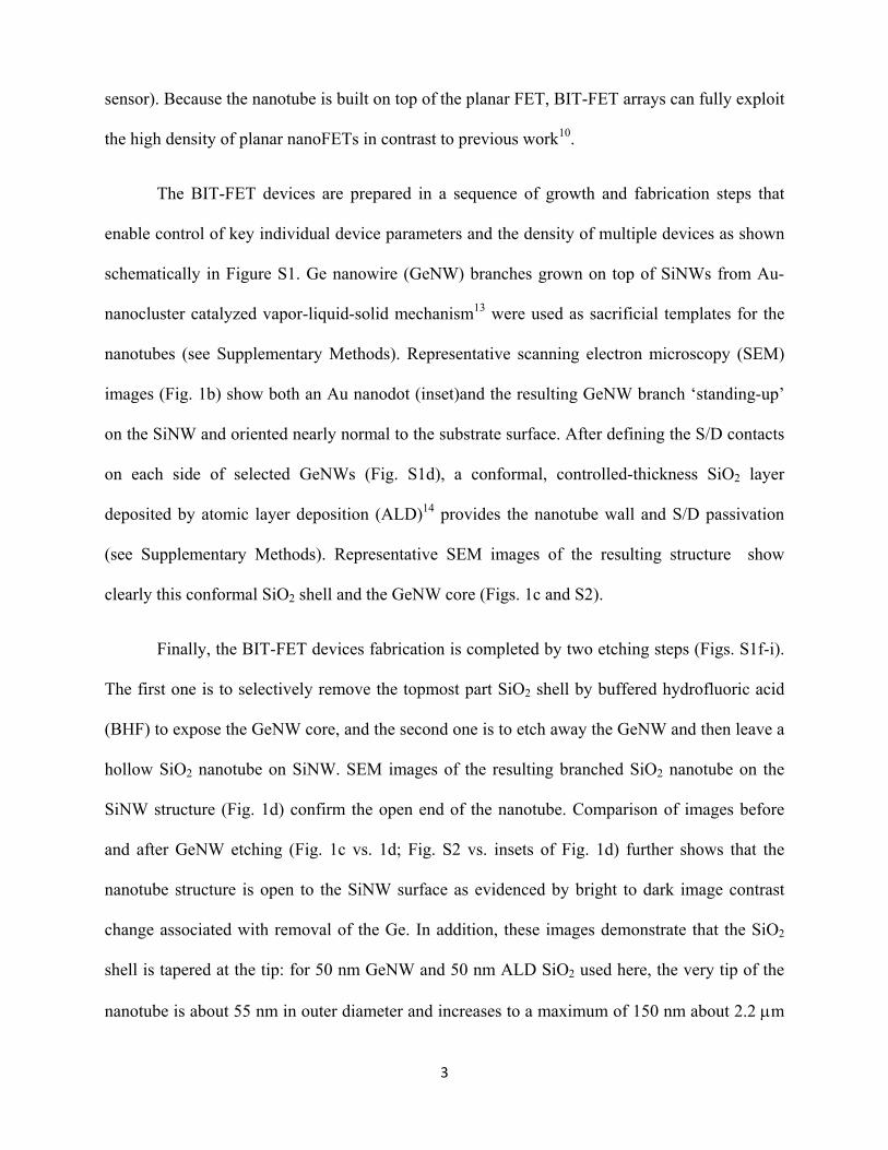
sensor). Because the nanotube is built on top of the planar FET, BIT-FET arrays can fully exploit
the high density of planar nanoFETs in contrast to previous work10.
The BIT-FET devices are prepared in a sequence of growth and fabrication steps that
enable control of key individual device parameters and the density of multiple devices as shown
schematically in Figure S1. Ge nanowire (GeNW) branches grown on top of SiNWs from Au-
nanocluster catalyzed vapor-liquid-solid mechanism13 were used as sacrificial templates for the
nanotubes (see Supplementary Methods). Representative scanning electron microscopy (SEM)
images (Fig. 1b) show both an Au nanodot (inset)and the resulting GeNW branch ‘standing-up’
on the SiNW and oriented nearly normal to the substrate surface. After defining the S/D contacts
on each side of selected GeNWs (Fig. S1d), a conformal, controlled-thickness SiO2 layer
deposited by atomic layer deposition (ALD)14 provides the nanotube wall and S/D passivation
(see Supplementary Methods). Representative SEM images of the resulting structure show
clearly this conformal SiO2 shell and the GeNW core (Figs. 1c and S2).
Finally, the BIT-FET devices fabrication is completed by two etching steps (Figs. S1f-i).
The first one is to selectively remove the topmost part SiO2 shell by buffered hydrofluoric acid
(BHF) to expose the GeNW core, and the second one is to etch away the GeNW and then leave a
hollow SiO2 nanotube on SiNW. SEM images of the resulting branched SiO2 nanotube on the
SiNW structure (Fig. 1d) confirm the open end of the nanotube. Comparison of images before
and after GeNW etching (Fig. 1c vs. 1d; Fig. S2 vs. insets of Fig. 1d) further shows that the
nanotube structure is open to the SiNW surface as evidenced by bright to dark image contrast
change associated with removal of the Ge. In addition, these images demonstrate that the SiO2
shell is tapered at the tip: for 50 nm GeNW and 50 nm ALD SiO2 used here, the very tip of the
nanotube is about 55 nm in outer diameter and increases to a maximum of 150 nm about 2.2 Pm
�
� 4
away from the tip. This tapering effect results from the isotropic etching of BHF (see
Supplementary Methods) and we believe that it is especially attractive for decreasing the size of
the probes.
We have characterized the electrical properties of the BIT-FETs and several control
devices in solution to elucidate the behavior of this new device architecture. A SEM image (Fig.
2a) shows a representative two-FET structure, where a BIT-FET and conventional FET with
similar channel length were fabricated with a common S electrode on the same SiNW. In both
devices, the SiNW and electrodes exposed to solution are passivated with about 50 nm ALD
SiO2 as described above. Measurements of conductance (G) for both devices as a function of
water-gate voltage (Vwg) prior to etching the GeNW core of the BIT-FET (Fig. 2b) show very
little change, with sensitivity of ca. -170 nS/V. Significantly, measurements made on the same
devices after removal of the GeNW core to yield an open nanotube structure (Fig. 2c),
demonstrate a large increase in the sensitivity of the BIT-FET to -4530 nS/V, while the control
SiNW FET shows no change. Taken together these results validate that BIT-FET devices
respond selectively and with high-sensitivity to the solution inside vs. outside the nanotubes, and
thus meet the requirements for intracellular recording outlined schematically in Fig. 1a. The
difference in sensitivity of the BIT-FET devices to solution inside vs. outside the nanotubes
originates primarily from the gate capacitance difference11,12. Specifically, Ge over-coating on
the SiNW may lead to a larger contact area between the SiNW and the internal solution of the
nanotube (the active FET area) than defined by the nanotube inner diameter, which can increase
this sensitivity difference (see Supplementary Methods).
We have also characterized the temporal response of BIT-FET devices to assess their
capability for recording fast cellular processes. A pulsed Vwg with 0.1 ms rise/fall time, 1 ms

�
� 5
duration and 100 mV amplitude was applied to approximate an action potential. The conductance
exhibits a peak (dip) coincident with the 0.1 ms rise (fall) of the pulse, and a plateau step down
during the constant 100 mV portion of the pulse (Fig. 2d). For pulsed Vwg measurement with
different rise/fall times from 0.1 to 50 ms, the conductance change associated with the baseline
to plateau is independent of the pulse rise time (Fig. 2e), and moreover, this change is consistent
with the device sensitivity determined from quasi-static measurements (e.g., Fig. 2c).
The peak and dip features in the pulsed Vwg results correspond to the expected capacitive
charging15 of the passivated metal electrodes and are not intrinsic to the BIT-FET. Specifically, a
control pulsed Vwg measurement made on a SiNW FET without a nanotube branch showed the
same peak (dip) features associated with the rapid rise (fall) of the Vwg pulse (Fig. S4a). These
capacitive features can be readily removed from the BIT-FET and control devices data to yield
the pure FET response (red curves, Fig. 2d and S4a, see Supplementary Methods), and in the
case of the BIT-FET, it demonstrates clearly that the conductance change follows the 0.1 ms Vwg
pulse rise/fall without detectable delay. The results shown in Fig. 2d and e demonstrate that the
BIT-FET can faithfully record potential changes with at least a 0.1 ms time resolution. Indeed,
our modeling (below) shows the temporal resolution, which is beyond our measurement
capabilities, should be much better than this value. We also note these capacitive features are not
expected in cellular measurements because (i) metal electrodes are only coupled to extracellular
media, where the potential changes are quite small16 and (ii) these changes will be localized on
the size of a cell, which is much smaller than the electrode area exposed to solution (~cm2) in the
pulsed Vwg experiments here.
In addition, we have modeled the BIT-FET device to estimate the bandwidth, which is
beyond our current measurement limit, and also investigated the bandwidth dependence on
�
� 6
nanotube diameter. The signal transduction in the BIT-FET device can be readily solved by the
classical transmission line model15. In our analysis (Fig. S4b, see Supplementary Methods), we
determine the change of the potential at the SiNW FET surface, Vn, as a function of time
following a step change of transmembrane potential at the nanotube opening to V0. For a typical
nanotube (inner diameter = 50 nm; ALD SiO2 thickness = 50 nm; length = 1.5 Pm), the
calculated response (inset, Fig. 2f) yields a bandwidth of ca. 1.2 MHz. This represents an upper
limit assuming the active FET area and relevant device capacitance CNW (Fig. S4b) is defined
only by the nanotube inner diameter, and could be reduced to 0.2 MHz if we assume the entire
SiNW surface is active due to Ge over-coating (see Supplementary Methods). A summary of
results (Fig. 2f) shows that the BIT-FET can achieve a bandwidth � 6 kHz, which is sufficient
for recording a rapid neuronal action potential1,2, for nanotube inner diameters as small as 3 nm
(fixed length = 1.5 Pm). The high bandwidth determined for the BIT-FET devices results in large
part from the small device capacitance, despite the increasingly large solution resistance within
the nanotube with decreasing inner diameter (see Supplementary Methods). The small diameters
accessible with the BIT-FET suggest that it could be minimally-invasive and capable of probing
the smallest cellular structures, including neuron dendrites and dendritic spines, which are
difficult using conventional electrical-based techniques17,18.
We investigated the capability of the BIT-FET to record intracellular signals using
spontaneously beating embryonic chicken cardiomyocyte cells, which were cultured on thin
pieces of polydimethylsiloxane (PDMS) as described previously16. After modifying the devices
with phospholipids10 to facilitate the internalization of nanotubes into cells, the PDMS/cell sheet
was manipulated to put a cell into gentle contact with the nanotube of a BIT-FET under standard
electrophysiology microscope (see Supplementary Methods). Approximately 45s after gentle
�
� 7
contact was made and in the absence of applied force to the cell substrate, the recorded data
showed a dramatic change (Fig. 3a). Before the transition, the signal exhibits a relatively flat
baseline with small biphasic peaks (5~8 mV amplitude; ~1 ms duration) with ca. 1 Hz frequency
(e.g., Figs. 3b, c). These peaks are coincident with cell beating and consistent with extracellular
recording reported previously16. Then the baseline shifts ca. -35 mV and new peaks with 75-100
mV amplitude and ~200 ms duration are observed (Fig. 3a). The recorded conductance data
yields inverted peaks for the p-type SiNW FETs used here, although the calibrated potentials are
consistent with standard peak polarity and shape of intracellular action potentials. These peaks
(e.g., Fig. 3d) have the shape and features characteristic of an intracellular action potential of
cardiomyocyte cells10,19,20, including fast depolarization at the beginning of the peak, plateau
region, fast repolarization, and hyperpolarization and return to baseline. The signal transition
from extra- to intracellular indicated the penetration of the cell by the nanotube. The baseline
shift is similar with that measured recently using kinked-nanowire probes10, but smaller than the
standard resting potential for cardiomyocytes19,20. Our reproducible and stable recording of full-
amplitude action potentials, which is a central result of our work, suggests that this baseline
difference is not due to poor sealing during nanotube internalization. We propose that the
discrepancy in resting potentials here could be attributed to a stronger suspension effect
introduced by the intracellular polyelectrolytes at the junction21,22 due to an order of magnitude
smaller size of SiO2 nanotube opening than a typical patch clamp pipette, although more detailed
studies will be required to quantitatively understand the origin of this effect. Although the
nanotube diameter routinely used in our intracellular recording studies, 50 nm inner diameter and
55 nm tip outer diameter, is larger than the smallest achievable for BIT-FETs (Fig. 2f), it is still

�
� 8
much smaller than the size of typical glass micropipettes1,2 and metal microelectrodes3,4,7 used
for intracellular studies.
The change from extracellular to intracellular signal without external force applied to cell
suggests the spontaneous penetration of cell membrane by the nanotube versus mechanical
insertion. We speculate that lipid fusion23,24 may play an important role in this penetration
similar to our previous observations10, and also that the small nanotube size is likely beneficial
for this lipid fusion process and the formation of a tight seal. There are several attractive
consequences of the spontaneous penetration. First, this typically leads to full-amplitude action
potential recording (e.g., Fig. 3) without circuitry to compensate for probe-membrane leakage,
thus suggesting tight sealing between the nanotube and cell membrane. Indeed, control
experiments carried out without phospholipids modification of the BIT-FETs required external
forces to achieve the transition to intracellular action potential signals, and the smaller amplitude
of these signals, 10-30 mV, suggests leakage at the nanotube-membrane interface3. Second, we
find that spontaneous penetration occurs in the same way for a broad range of nanotube
orientation (i.e., within 30o of the surface normal), which contrasts mechanical insertion. Third,
we believe that the tight nanotube-membrane seal and the very small nanotube internal volume,
ca. 3 aL, help to preserve cell viability and a stable signal over time. In general, we find that
termination of signal recording by the BIT-FET is due to random separation of the nanotube
from the motion of the beating cardiomyocyte cell and not cell death or degradation of the
nanotube/cell membrane interface, where the latter normally occur during recording with glass
micropipettes1,2. In addition and unlike a glass micropipette, when the BIT-FET nanotube is
separated from a cell (on purpose as shown below or by the beating motion), the nanotube can
re-penetrate into the same cell multiple times at approximately the same position without

�
� 9
affecting the cell or recorded signal (see below). Last, we note that the total recording time from
multiple penetrations at a given position on a cell with the BIT-FET can exceed an hour.
We also find that the BIT-FET devices are robust and reusable. Specifically, following
retraction of the cell substrate from the device, which results in return of the conductance to the
extracellular baseline, subsequent gentle contact of the nanotube to the same cell without
changing position leads to the development of stable intracellular action potential signals again
(Fig. 3e). We have repeated the gentle contact/intracellular recording/retraction cycle up to five
times with the same BIT-FET nanotube near the same position on the cell without observable
change in the beating frequency and action potential features. A SEM image of the BIT-FET
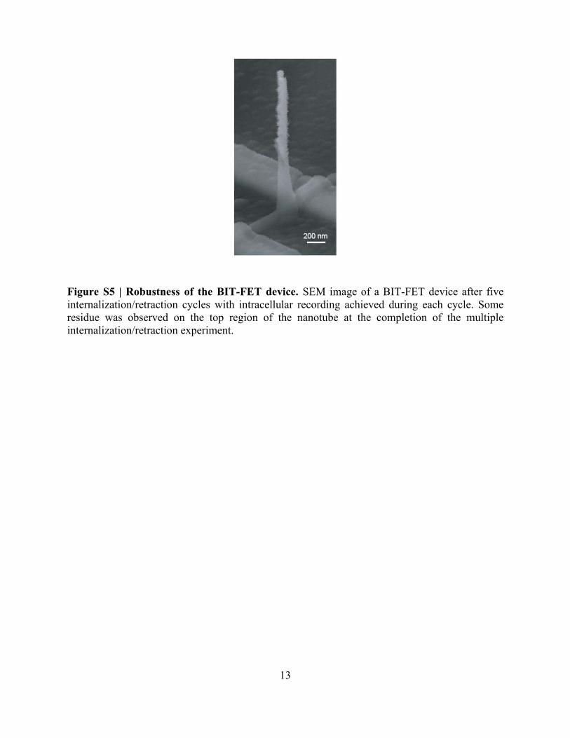
device following these repeated cycles (Fig. S5) shows that the nanotube remains intact with
some residue on the upper outer surface. In addition, we did not see evidence for the blockage of
the nanotube during these cycles, which we attribute to spontaneous penetration versus suction or
mechanical insertion. Furthermore, we note that devices can even be reused after being dried.
Taken together these results demonstrate the reliability and robustness of the BIT-FETs and
strongly indicate that this is a minimally-invasive intracellular recording technique.
A unique feature of the BIT-FET design is the straightforward fabrication of multiple,
independent devices to enable multiplexed recording from single cells through cell networks.
For example, we have readily aligned two phospholipid-modified BIT-FET devices separated by
about 20 Pm with a single, beating cardiomyocyte cell (Fig. 4a). Following gentle contact,
conductance versus time measurements made simultaneously from both devices (Fig. 4b) show
that device-1 first bridged the cell membrane to yield clear intracellular signals, and ~10s later
we observed the development of intracellular peaks from device-2. Subsequently, intracellular
signals were recorded from both devices (e.g. Fig. 4c). We can glean several important points
�
� 10
from these data. First, the sequential nature by which the intracellular signals develop, in the
absence of an applied force, strongly supports the suggestion above that penetration of the
phospholipid-modified nanotubes is a spontaneous biomimetic process that does not adversely
affect the cell rather than mechanical insertion. Second, the intracellular peaks recorded
simultaneously by devices-1 and -2, with full amplitude of 75-100 mV, and stable cell beating
over time are consistent with the tight seal being established between the cell membrane and the
nanotubes in both devices. In addition, we have also demonstrated that multiplexed
measurements with BIT-FETs can be extended to cell networks (Figs. 4d & e), where we record
intracellular action potentials simultaneously from different sites in a monolayer of beating
cardiomyocyte cells. In the future, we note that this BIT-FET design is implementable on high
density integrated planar nanoFETs, either large arrays of nanowire FETs25 or conventional top-
down nanoFET arrays26, to enable multiplexed recording at a far higher density than
demonstrated in these initial studies.
Additional work remains to improve further the BIT-FET based intracellular
measurement technique. The signal-to-noise ratio is still lower than that of glass micropipette.
And implementing the capability for cell stimulation in addition to recording is also important
for intracellular study. However, we believe the advantages of the BIT-FET demonstrated in this
work, including the capability to realize sub-5 nm size probes, the formation of tight nanotube-
cell membrane seals, and the potential for large-scale high-density multiplexed recording, make
it an attractive new measurement tool to extend substantially the scope of fundamental and
applied electrophysiology studies to regimes hard to access by current methods.
�
� 11
Methods Summary
SiNWs were synthesized using Au-nanocluster catalysed VLS growth described
previously16. After dispersing SiNWs on Si3N4 surface of silicon wafers, Au nanodots were
defined on the top surfaces of the SiNWs by electron-beam lithography (EBL) and metal
evaporation, and GeNW branches were grown from these nanodots by another Au-catalysed
VLS step. Source and drain metal contacts were defined by EBL and metal evaporation on each
side of selected GeNW branches on the corresponding SiNW backbones, and then a conformal
and uniform SiO2 layer was then deposited on the entire chip by ALD. Photoresist was spin-
coated with thickness smaller than the selected GeNW branches height, and then BHF was used
to remove the SiO2 from the exposed tips of the GeNW/SiO2 core/shell structure. Following
photoresist lift-off, H2O2 was used to etch the GeNW cores and yield the final BIT-FET devices.
Conductance versus Vwg measurements were carried out in 1uPBS buffer using an Ag/AgCl
electrode. Electrical recordings from embryonic chicken cardiomyocytes were carried out using
methods published previously10,16, with cells cultured on thin PDMS films and device chips
modified with lipid layers. A glass micropipette was used to control the relative position between
the cell and the nanotube(s) of BIT-FET device(s), and Ag/AgCl reference electrodes were used
to fix the extracellular solution potential. The BIT-FET bandwidth as a function of nanotube ID
was determined from simulations of the time-dependent change in potential at the SiNW FET
surface, Vn, following a potential step change at the open nanotube end.

�
� 12
References:
1. Sakmann, B. & Neher, E. Patch clamp techniques for studying ionic channels in excitable
membranes. Ann. Rev. Physiol. 46, 455-472 (1984).
2. Molleman, A. Patch clamping: an introductory guide to patch clamp electrophysiology
(Wiley, Chichester, England, 2003).
3. Rutten, W. L. C. Selective electrical interfaces with the nervous system. Annu. Rev.
Biomed. Eng. 4, 407-452 (2002).
4. Purves, R. D. Microelectrode methods for intracellular recording and ionophoresis
(Academic Press, London, 1981).
5. Chorev, E., Epsztein, J., Houweling, A. R., Lee, A. K. & Brecht, M. Electrophysiological
recordings from behaving animals-going beyond spikes. Curr. Opin. Neurobiol . 19, 513-
519 (2009).
6. Dunlop, J., Bowlby, M., Peri, R., Vasilyev, D. & Arias, R. High-throughput
electrophysiology: an emerging paradigm for ion-channel screening and physiology. Nat.
Rev. Drug Discovery 7, 358-368 (2008).
7. Hai, A., Shappir, J. & Spira, M. E. In-cell recordings by extracellular microelectrodes.
Nat Methods. 7, 200-U50 (2010)
8. Schrlau, M. G., Dun, N. J., & Bau, H. H. Cell electrophysiology with carbon nanopipettes.
ACS Nano 3, 563-568 (2009).
9. de Asis, E. D., Leung, J., Wood, S., & Nguyen, C. V. High spatial resolution single
multiwalled carbon nanotube electrode for stimulation, recording, and whole cell voltage
clamping of electrically active cells. Appl. Phys. Lett. 95, 153701 (2009).
10. Tian, B. et al. Three-dimensional, flexible nanoscale field-effect transistors as localized
bioprobes. Science 329, 831-834 (2010).
11. Sze, S. M. & Ng, K. K. Physics of Semiconductor Devices, 3rd Edition (Wiley-
interscience, 2006).
12. Patolsky, F., Zheng, G. & Lieber, C. M. Nanowire-Based Biosensors. Anal. Chem. 78,
4260-4269 (2006).
13. Jiang, X. et al., Rational growth of branched nanowire heterostructures with
synthetically-encoded properties and function. Proc. Natl. Acad. Sci. USA 108, 12212-
12216 (2011).

�
� 13
14. Hausmann, D., Becker, J., Wang, S. & Gordon, R. G. Rapid vapor deposition of highly
conformal silica nanolaminates. Science 298, 402-406 (2002).
15. Sadiku, M. N. O. Elements of Electromagnetics. 3rd edition. (Oxford University Press,
USA, 2000).
16. Cohen-Karni, T., Timko, B. P., Weiss, L. E. & Lieber, C. M. Flexible electrical recording
from cells using nanowire transistor arrays. Proc. Natl. Acad. Sci. USA 106, 7309-7313
(2009).
17. Scanziani, M. & Hausser, M. Electrophysiology in the age of light. Nature 461, 930-939
(2009).
18. Davie, J. T. et al. Dendritic patch-clamp recording. Nat. Protoc. 1, 1235-1247 (2006).
19. Bers, D. M. Cardiac excitation-contraction coupling. Nature 415, 198-205 (2002).
20. Zipes, D. P. & Jalife, J. Cardiac electrophysiology: from cell to bedside, 5th edition
(Saunders, Philadelphia, PA, 2009).
21. Buck, R. P. & Grabbe, E. S. Electrostatic and thermodynamic analysis of suspension
effect potentiometry. ANAL. CHEM. 58, 1938-1941 (1986).
22. Tasaki, I. & Singer, I. Some problems involved in electric measurements of biological
systems. ANN. NY. ACAD. SCI. 148, 36-53 (1968).
23. Chernomordik, L. V. & Kozlov, M. M. Mechanics of membrane fusion. Nature Struct.
Mol.Biol. 15, 675-683 (2008).
24. Almquist, B. D. & Melosh, N. A. Fusion of Biomimetic Stealth Probes into Lipid Bilayer
Cores. Proc. Natl. Acad. Sci. USA�107, 5815-5820 (2010).
25. Yan, H. et al. Programmable nanowire circuits for nanoprocessors. Nature 470, 240-244
(2011).
26. International Technology Roadmap for Semiconductors. Available online at
http://www.itrs.net. (2009 Edition).
Acknowledgements We thank Z. Jiang and H. Yan for helpful discussions. R.G. acknowledges
Japan Student Services Organization Graduate Research Fellowship. C.M.L. acknowledges
support of this work by a NIH Director’s Pioneer Award 5DP1OD003900.
Author Contributions X.D. and C.M.L. designed the experiments. X.D., R.G, T.C.-K., Q.Q., H.S.C. and B.T.
performed experiments. X.D., P.X. and Q.Q. performed modeling and analyses. X.D., P.X., Q.Q. X.J. and C.M.L.

�
� 14
analyzed data. X.D., P.X., and C.M.L. wrote the paper. All authors discussed the results and commented on the
manuscript.
Competing financial interests: The authors declare that they have no competing financial interests.
�
� 15
Figure Legends
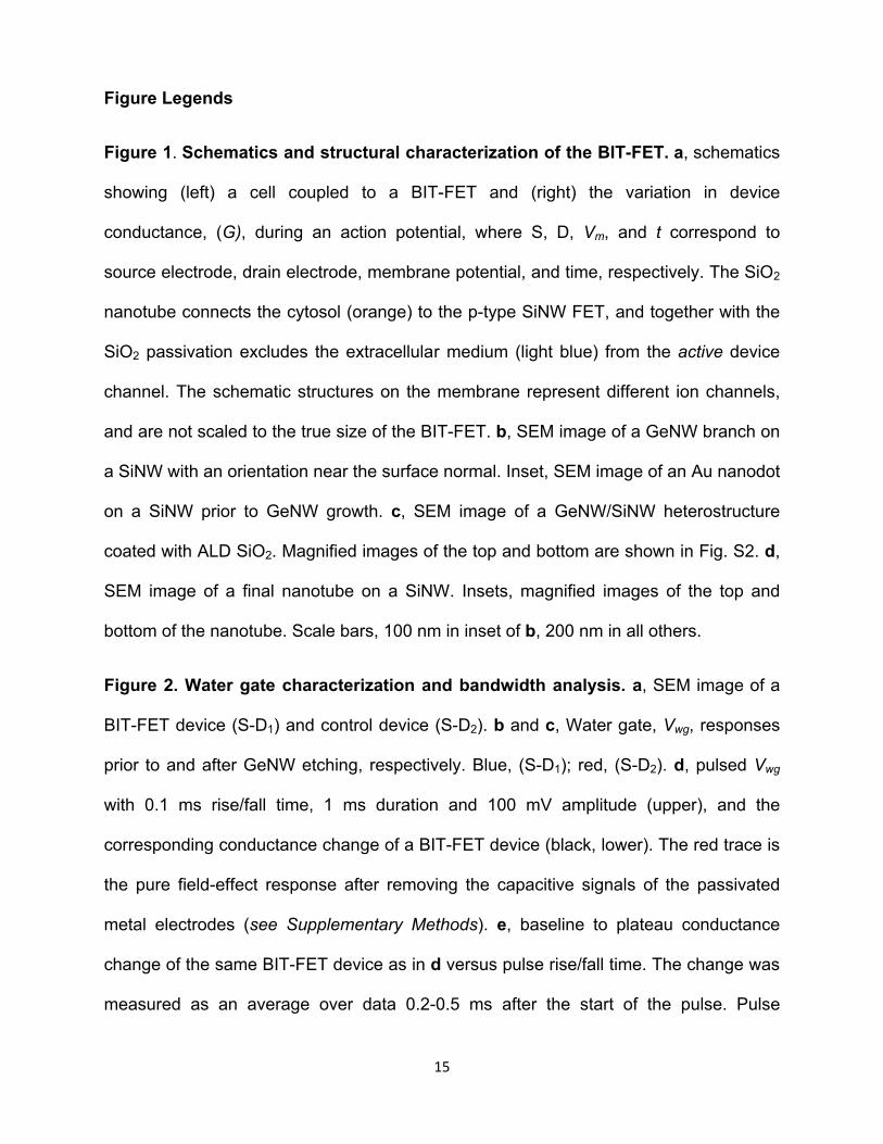
Figure 1. Schematics and structural characterization of the BIT-FET. a, schematics
showing (left) a cell coupled to a BIT-FET and (right) the variation in device
conductance, (G), during an action potential, where S, D, Vm, and t correspond to
source electrode, drain electrode, membrane potential, and time, respectively. The SiO2
nanotube connects the cytosol (orange) to the p-type SiNW FET, and together with the
SiO2 passivation excludes the extracellular medium (light blue) from the active device
channel. The schematic structures on the membrane represent different ion channels,
and are not scaled to the true size of the BIT-FET. b, SEM image of a GeNW branch on
a SiNW with an orientation near the surface normal. Inset, SEM image of an Au nanodot
on a SiNW prior to GeNW growth. c, SEM image of a GeNW/SiNW heterostructure
coated with ALD SiO2. Magnified images of the top and bottom are shown in Fig. S2. d,
SEM image of a final nanotube on a SiNW. Insets, magnified images of the top and
bottom of the nanotube. Scale bars, 100 nm in inset of b, 200 nm in all others.
Figure 2. Water gate characterization and bandwidth analysis. a, SEM image of a
BIT-FET device (S-D1) and control device (S-D2). b and c, Water gate, Vwg, responses
prior to and after GeNW etching, respectively. Blue, (S-D1); red, (S-D2). d, pulsed Vwg
with 0.1 ms rise/fall time, 1 ms duration and 100 mV amplitude (upper), and the
corresponding conductance change of a BIT-FET device (black, lower). The red trace is
the pure field-effect response after removing the capacitive signals of the passivated
metal electrodes (see Supplementary Methods). e, baseline to plateau conductance
change of the same BIT-FET device as in d versus pulse rise/fall time. The change was
measured as an average over data 0.2-0.5 ms after the start of the pulse. Pulse
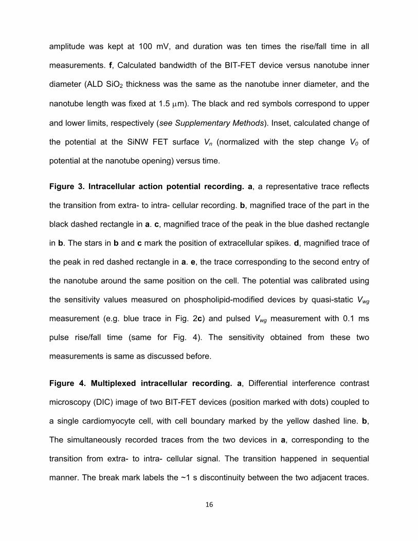
�
� 16
amplitude was kept at 100 mV, and duration was ten times the rise/fall time in all
measurements. f, Calculated bandwidth of the BIT-FET device versus nanotube inner
diameter (ALD SiO2 thickness was the same as the nanotube inner diameter, and the
nanotube length was fixed at 1.5 Pm). The black and red symbols correspond to upper
and lower limits, respectively (see Supplementary Methods). Inset, calculated change of
the potential at the SiNW FET surface Vn (normalized with the step change V0 of
potential at the nanotube opening) versus time.
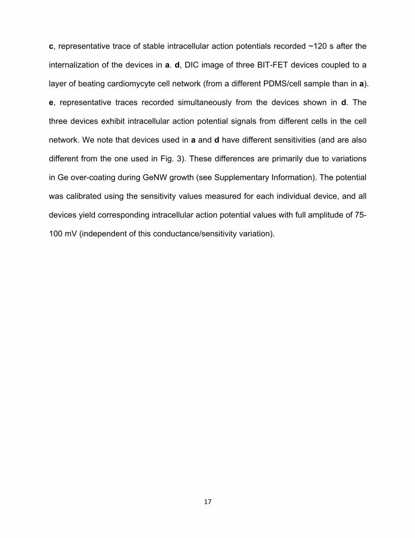
Figure 3. Intracellular action potential recording. a, a representative trace reflects
the transition from extra- to intra- cellular recording. b, magnified trace of the part in the
black dashed rectangle in a. c, magnified trace of the peak in the blue dashed rectangle
in b. The stars in b and c mark the position of extracellular spikes. d, magnified trace of
the peak in red dashed rectangle in a. e, the trace corresponding to the second entry of
the nanotube around the same position on the cell. The potential was calibrated using
the sensitivity values measured on phospholipid-modified devices by quasi-static Vwg
measurement (e.g. blue trace in Fig. 2c) and pulsed Vwg measurement with 0.1 ms
pulse rise/fall time (same for Fig. 4). The sensitivity obtained from these two
measurements is same as discussed before.
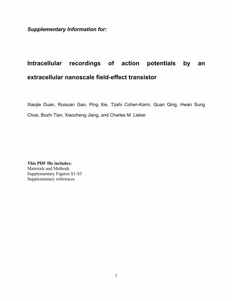
Figure 4. Multiplexed intracellular recording. a, Differential interference contrast
microscopy (DIC) image of two BIT-FET devices (position marked with dots) coupled to
a single cardiomyocyte cell, with cell boundary marked by the yellow dashed line. b,
The simultaneously recorded traces from the two devices in a, corresponding to the
transition from extra- to intra- cellular signal. The transition happened in sequential
manner. The break mark labels the ~1 s discontinuity between the two adjacent traces.
�
� 17
c, representative trace of stable intracellular action potentials recorded ~120 s after the
internalization of the devices in a. d, DIC image of three BIT-FET devices coupled to a
layer of beating cardiomycyte cell network (from a different PDMS/cell sample than in a).
e, representative traces recorded simultaneously from the devices shown in d. The
three devices exhibit intracellular action potential signals from different cells in the cell
network. We note that devices used in a and d have different sensitivities (and are also
different from the one used in Fig. 3). These differences are primarily due to variations
in Ge over-coating during GeNW growth (see Supplementary Information). The potential
was calibrated using the sensitivity values measured for each individual device, and all
devices yield corresponding intracellular action potential values with full amplitude of 75-
100 mV (independent of this conductance/sensitivity variation).

a
b c d
extracellular fluid
SiO2
cytosol
t
Vm action potential
p-SiNWsubstrate
S D
Vm
A
S Dp-SiNW
tG
Figure 1

1.0
0.6
0.2
1.00.60.2
∆G (
S)
a
b
c
d
e
D2
S
D1
200 nm
43.5
43.0
42.5
42.0
41.5
G (
S)
0.20.10.0-0.1-0.2Vwg (V)
42.5
42.0
41.5
41.0
40.5
2.0
1.5
1.0
0.5
0.0
80400
Time (ms)3.02.01.00.0
0 10 20 30 40 50Rise time (ms)
0.66
0.68
0.70Vwg (mV)
G (
S)
50403020100Nanotube ID (nm)
Time ( s)
Vn / V
0
104
105
106
Bandw
idth (H
z)
f
solution
solution
G (
S)
0.20.10.0-0.1-0.2Vwg (V)
Figure 2

1st entry
2nd entry
20 mV 200 nS1 s
3 mV 30 nS500 ms
3 mV 30 nS10 ms
20 mV 200 nS
100 ms
20 mV 200 nS1 s
a
b
c
d
e
Figure 3

2.26
2.16
30.54
30.34
2.88
2.73
10 m
Device-1
Device-2
a b
Device-1G (
S)
2 sDevice-2
67.06
67.04
67.02
34.86
34.83
34.80
67.04
67.02
67.00
34.86
34.83
34.80
G (
S)
Device-1
2 s Device-230 m
Device-1
Device-3
Device-2
G (
S)
Device-1
Device-2
Device-3
c d e
1 s
Figure 4
1
Supplementary Information for: Intracellular recordings of action potentials by an
extracellular nanoscale field-effect transistor
Xiaojie Duan, Ruixuan Gao, Ping Xie, Tzahi Cohen-Karni, Quan Qing, Hwan Sung
Choe, Bozhi Tian, Xiaocheng Jiang, and Charles M. Lieber
This PDF file includes: Materials and Methods Supplementary Figures S1-S5 Supplementary references

2
Materials and Methods
Nanowire nanostructure synthesis. Single crystal p-doped silicon nanowires (p-SiNWs) were
synthesized by the nanocluster-catalyzed vapor-liquid-solid (VLS) process as described
previously1. Briefly, 100 nm diameter gold nanoparticles (Ted Pella) were dispersed on SiO2/Si
growth substrates (Nova Electronic Materials), and growth was carried out at a total pressure of
25 torr, temperature of 450–460 °C, using SiH4 (2.5 sccm), B2H6 (3 sccm, 100 ppm in He) and
Ar carrier (10 sccm) for 20~30 mins. The resulting ca. 100 nm diameter p-SiNWs grown as
above were deposited from an isopropanol dispersion onto Si3N4 surface of silicon wafers (100
nm thermal SiO2, 200 nm Si3N4, n-type, 0.005 V · cm, Nova Electronic Materials). Germanium
nanowire (GeNW) branches, which serve as the template for the final nanotube structures, were
also synthesized by the Au nanocluster catalyzed VLS process. A modification of the sequential
branch growth process described previously2 was used (Figs. S1a-c). First, Au nanodots were
defined by electron-beam lithography (EBL, JEOL JSM-7000F) and metal evaporation on the
top surfaces of the dispersed SiNWs, the chip was placed in the growth reactor, and then GeNW
branches were grown using an initial nucleation step at 305-315 °C for 5 min (GeH4 (10 sccm,
10% in H2), H2 (200 sccm), total pressure of 100 torr) and elongation step at 280-295 °C for 20
min (gas flow and pressure same as for nucleation). The GeNW branch diameter, which defines
the final SiO2 nanotube inner diameter (ID), is controlled through the size and thickness of the
deposited Au nanodots. And the growth with Au nanodots of 80 nm diameter and 40 nm
thickness yielded average 50 nm GeNW branches on top of SiNW backbones. The GeNW
lengths are determined by the growth time with typical values of 2-4 Pm. The specific
orientation of the GeNWs was not controlled in these studies because the penetration of the
nanotubes into cells does not require them to be vertical (see main text). For this reason, we
selected and used GeNWs within 30o with respect to the surface normal for BIT-FET devices
(see below). We note that alternative methods, such as chemical reduction from solution, can be
used to prepare Au particles on SiNWs (without the need for EBL) for GeNW branch growth2 in
a parallel and high-throughput manner.
BIT-FET device fabrication. Completion of the nanotube structure and device fabrication were
carried out in parallel as shown schematically in Fig. S1. Following GeNW branch growth, resist
was coated on the chip (~2 Pm copolymer, MMA (8.5) MAA (EL11) and ~0.5 Pm PMMA (950

3
C5), MicroChem Corp.), baked at 180 °C for 10 min. Then EBL and thermal evaporation were
used to define Ti/Pd/Ti (1.5/120/10 nm) S/D contacts on each side of selected GeNW branches,
which are within 30o with respect to the surface normal, on the corresponding SiNW backbones
(Fig. S1d). The typical separation between S/D contacts was 300-700 nm. Critical point drying
(Auto Samdri 815 Series A, Tousimis,) was used during lift-off and rinse steps to minimize
collapse of the GeNW branches. A uniform layer of SiO2 (~50 nm) was deposited by atomic
layer deposition (ALD, Savannah-S200, Cambridge NanoTech) at 250 °C3, and annealed in the
ALD system at 250 °C for 15 min. The conformal SiO2 layer (Fig. S1e) serves both as the
nanotube wall (after removal of Ge) and passivation of the metal electrodes. The GeNW core is
removed by a sequence of steps shown in Fig. S1 (f-i) to yield the final nanotube device. First, A
photoresist protection layer (Shipley S1813 or S1818, MicroChem Corp.) was coated to a
thickness smaller than the GeNWs height, baked at 115 °C for 5 min, and then the exposed SiO2
of the GeNW/SiO2 core/shell structure was removed by BHF (Buffered HF Improved, Transene)
(20~25 s for ~50 nm ALD SiO2). The BHF etching goes along both the radial and axial direction,
which results in a tapered SiO2 shell. Following photoresist lift-off, hydrogen peroxide (H2O2,
30%, Sigma) was used to selectively etch the Ge (50 ºC, 45-60 min). The final SiO2 nanotube
height is defined by the thickness of the photoresist protection layer. Unless specifically
mentioned, all devices used in this work, including those for device characterization and cell
measurements etc., use nanotube inner diameter and ALD SiO2 thickness of ca. 50 nm, nanotube
length of 1-1.5 Pm, p-doped SiNWs with diameter of ca. 100 nm.
Device characterization. To characterize the response of the BIT–FET devices in aqueous
solution, a 2 mm thick polydimethylsiloxane (PDMS) sheet with a 15 mm u 10 mm window was
put on the device chip, and the open region was filled with 1u phosphate buffered saline (PBS,
Mediatech, Inc.); a Ag/AgCl electrode was inserted into the solution and the FET conductance
versus water gate voltage (Vwg) measurements were carried out by sweeping the voltage while
simultaneously recording the FET current with a current preamplifier (1211, DL Instruments).
The voltage sweep output/preamplifier output was generated/recorded with a DAC card (PCI-
6030E, National Instruments, Inc.) under computer control, with typical ramp speed of 50 mV/s.
To assess the temporal response of the BIT-FET devices, a pulsed Vwg with variable rise time
(0.1-50 ms) was generated (Axon Digidata 1440A Data Acquisition System, Molecular Devices,
4
Inc.) and the current of the FET was amplified with a home-built current preamplifier, filtered
(CyberAmp 380, Molecular Devices, Inc.), and then digitized (Axon Digidata 1440A Data
Acquisition System, Molecular Devices, Inc.). Conductance values recorded for BIT-FET
devices vary between ca. 1-70 PS. This variation reflects differences in the SiNWs and device
configuration, but has no effect on calculated potentials since the sensitivity of each device was
determined prior to cell measurements.
BIT-FET sensitivity. The sensitivity, which is characterized by the conductance change per unit
Vwg change (transconductance) is proportional to the gate capacitance4. Before GeNW etching
(Fig. S3a), the relevant gate capacitance, which reflects the sensitivity of BIT-FET to the
solution outside the nanotube, can be estimated5 with the half cylindrical model (inset, Fig. S3a)
as:
Cout = ʌİ0İrL/ln[(dSiNW+2tSiO2)/dSiNW] (1)
where İ0, İr, L, dSiNW and tSiO2 are vacuum dielectric constant, relative dielectric constant of SiO2,
effective channel length, SiNW diameter and ALD SiO2 thickness,
L = Lapp-dbase-4tSiO2 (2)
Lapp is the distance between the two closest edges of S/D electrodes (apparent channel length),
dbase is the diameter of the GeNW branch base, which is normally larger than the diameter of the
GeNW branch body (c.a. 100 nm for 50 nm average diameter GeNW, e.g. Fig. 1b).
After removing the GeNW, solution fills in nanotube and gates the SiNW FET through the thin
(1.5 nm, tnative as below) native oxide (Fig. S3b). We model the capacitance, Cin, which reflects
the sensitivity of the BIT-FET to solution inside the nanotube, as a parallel plate capacitor5:
Cin=İ0İrA/tnative (3)
where A is the contact area between the SiNW and the solution inside the nanotube. If there is no
Ge over-coating, A is equal to the GeNW base area. The transconductance ratio after to before
GeNW etching is estimated by the gate capacitance ratio, (Cin+Cout)/Cout. For the device used in
Fig. 2 a-c, this yields a ratio, ~5, which is smaller than the experimental value, ~26.
5
The enhanced sensitivity difference compared to the idealized calculation is a result of several
factors. First, the contact area A can be larger than that defined by the GeNW branch base due to
over-coating of Ge on SiNW surface during GeNW growth. Removal of this Ge material over-
coated on SiNWs during etching will lead to a longer active channel, and larger A and Cin. We
note that SEM images of the BIT-FETs taken after breaking nanotubes at the SiNW-tube
junction always show a larger hole than would be defined by GeNW branch base alone, which is
consistent with a larger A. The upper limit in this context, which corresponds to the entire SiNW
surface exposed to the internal solution of the nanotube, would yield a sensitivity ratio of ~50.
The experimental ratio falls between these calculated limits, which suggests that the active
channel exposed to the internal solution of nanotube is smaller than the entire SiNW surface but
larger than that defined by the GeNW base. Indeed, device measurements show a range of
enhancement ratios and the transconductance/sensitivity values for different BIT-FETs vary for
different GeNW growth conditions (different Ge over-coating). We note that because all device
sensitivities are characterized, the observed variation does not affect our determination of
absolute potential change in the cell measurements. In the future, we anticipate that Ge over-
coating could be used to rationally enhance the sensitivity of the BIT-FET devices. Second, the
small effective channel length L and relatively thick SiO2 dielectric layer can lead to a reduction
in Cout due to the screening by the metal S/D electrodes6. This would lead to a lower sensitivity
than estimated for the BIT-FET prior to GeNW etching.
Pulsed water gate curve fitting. In the pulsed Vwg measurement, the capacitive coupling current
between the passivated metal electrodes (in the open window area) and the solution yield +/-
peaks in during the rising/falling edges of the pulse (e.g., Figs. 2d and S4a). To accurately
remove these artifacts without affecting the intrinsic BIT-FET signal we carried out the
following steps. First, a control device without SiO2 nanotube was fabricated and measured
(black trace, Fig. S4a), where the baseline conductance (before and after pulse) and the steady
state conductance during the pulse represents the intrinsic SiNW FET response (red trace, Fig.
S4a). The +/- peaks obtained by subtracting the intrinsic FET response from the measured data
for the control device, yields the pure capacitive coupling signal for the control device. The
capacitive coupling signal determined from this analysis for the control device was then scaled
by ratio of the exposed electrode areas for the BIT-FET versus control devices, to yield the

6
capacitive coupling signal of the BIT-FET device, which is then subtracted from the measured
data to yield intrinsic device response (red trace, lower panel of Fig. 2d). Note that the
subtraction has no fitting parameters and the capacitive coupling artifacts are removed
completely.
Cell recording. Embryonic chicken cardiomyocytes were cultured using published protocols on
thin PDMS films7,8. Device chips were incubated with lipid vesicles of 1,2-dimyristoyl-sn-
glycero-3-phosphocholine (DMPC, Avanti Polar Lipids Inc.) containing 1% 1-myristoyl-2-{12-
[(7-nitro-2-1,3-benzoxadiazol-4-yl) amino] dodecanoyl}-sn-glycero-3-phosphocholine (NBD-
lipid, Avanti Polar Lipids Inc.) as fluorescent reporter to form supported lipid layers on devices
including nanotube surfaces, using a procedure described earlier8. The cell recording
measurements were carried out in tyrode solution (pH ~ 7.3) at 30-37°C using a 100 mV DC
source voltage for FET devices. The current was amplified with a home-built multi-channel
current preamplifier, filtered with a 6 kHz low pass filter (CyberAmp 380), and digitized at 50-
250 kHz sampling rate (Axon Digi1440A). Ag/AgCl reference electrodes were used to fix the
extracellular solution potential in all recording experiments7,8. The PDMS/cell sheets were
manipulated using glass micropipettes to control the relative position between the cells and the
nanotubes.
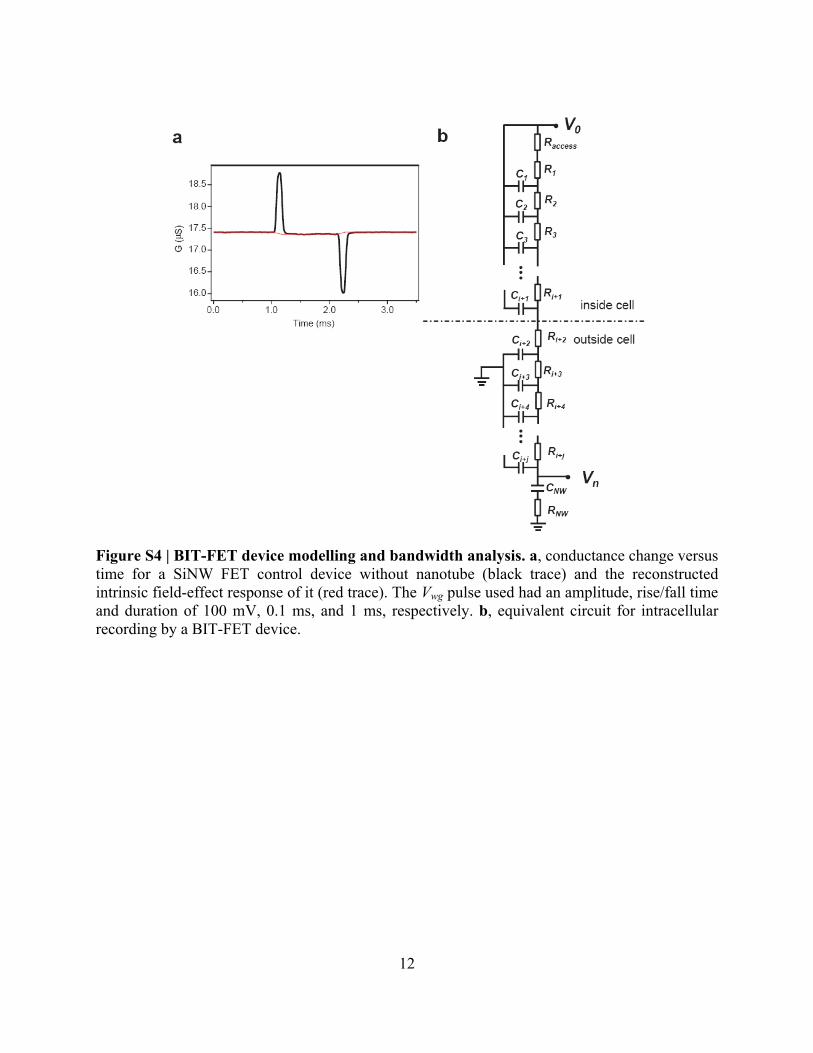
Bandwidth calculation. The BIT-FET device was modeled by the equivalent circuit shown in
Fig. S4b. Resistors R1, …, Ri+j are used to model the distributed resistance of the solution inside
the nanotube, capacitors C1, …, Ci+j model the distributed capacitance between the inside and
outside of the nanotube, Raccess is the access resistance from the solution to the opening of the
nanotube, V0 is the intracellular potential of the cell. Outside the cell, the solution outside the
nanotube is fixed by the reference electrode, Vn is the potential at the end of the nanotube (SiNW
surface), CNW is the gate capacitance of SiNW accessed by the internal solution in nanotube, and
RNW is the resistance of the SiNW. The cell electrical potential signal propagates from the
opening of the nanotube to its end, where it couples to the FET channel, through the solution.
The potential also capacitively couples to the solution outside the nanotube across the SiO2
nanotube wall. Using the Ohm’s law and capacitive coupling5 at any point along the nanotube,
the propagation of the electrical potential signal can be described by:

7
( )
inR
in outC
V Iz
V VIz t
U
U
w� °° w® w �w°� ° w w¯
(4)
Here Vin, Vout, ȡR, ȡC, I, z, t are potential inside the nanotube, potential outside the nanotube,
linear resistivity of solution inside the nanotube (resistance per unit length), capacitance of the
nanotube wall per unit length, current, distance from the nanotube opening, and time,
respectively. These equations can be rewritten as:
2
2 ( )in in outR C
V V Vz t t
U Uw w w �
w w w (5)
where ȡR is calculated from the solution bulk resistivity ȡBulk by ȡR=4ȡBulk/ʌd2 and ȡC comes from
three parts connected in series: the two electrical double layers on the inner and outer SiO2
surface of the nanotube, and the capacitance across the SiO2 wall. Each part is calculated from
the cylindrical capacitor model5 by ȡC = 2ʌİİ0/ln(a2/a1), where İ is the dielectric constant of the
material, a1 and a2 is the inner and outer diameter of the cylinder. For example, the capacitance
across the SiO2 wall can be written as ȡC=2ʌİrİ0/ln [(d+2tSiO2)/d]. Here d is the nanotube inner
diameter. İr, İ0, and tSiO2 are defined as before in the ‘BIT-FET sensitivity’ part. Overall, the
capacitance of the SiO2 wall is the dominant term due tothe large thickness of the SiO2 wall and
the relatively small dielectric constant of SiO2 (compared to the water double layer dielectric
constant), although we considered all three parts in the calculation.
We evaluate the potential change at the end of the nanotube as a function of time following cell
potential change, based on equation (5), using 1-dimensional finite element method (written in
Mathematica, Wolfram Research, Inc.). The boundary conditions for the simulation are as
follows: Outside the cell, Vout is fixed by the reference electrode; inside the cell, Vout equals to the
intracellular potential of the cell; 1/3 of the nanotube is inside the cell; the gate capacitance, CNW,
of the SiNW is approximated as a parallel plate capacitor.
The bandwidth is evaluated by using a fast ramp of the cell potential from 0 to the steady-state
value V0, and simulating the corresponding change of the potential at the end of the nanotube Vn
vs. time. The effective bandwidth, BW, is:

8
0.35 /BW W| (6)
where IJ is the time for Vn to change from 10 % to 90 % of V0. For the calculation of the diameter-
dependent bandwidth (Fig. 2f), the SiO2 thickness was fixed at the nanotube ID, and the
nanotube length was a constant 1.5 Pm. The high bandwidth determined for the BIT-FET
devices results in large part from the small device capacitances, despite the increasingly large
solution resistance within the nanotube with decreasing ID. For example, the resistance of
physiological solution inside a 10 nm ID, 1.5 Pm long nanotube is ca. 19 G:, but the
corresponding capacitance is only 0.3 fF.
The above simulation gives the upper limit bandwidth for our BIT-FETs. When the active
channel extends beyond the area defined by the GeNW base due to the Ge over-coating (see
sensitivity discussion above), the bandwidth will decrease. The lower-limit bandwidth for this
configuration (red data points, Fig 2f) was calculated using the same finite element method by
assuming a 10 nm gap between SiNW and ALD SiO2, and 400 nm active SiNW channel length.

9
Figure S1 | Schematic fabrication flow for the BIT-FET device. a, SiNW is dispersed on substrate. b, Au nanodot is defined on the SiNW using EBL and thermal evaporation. c, GeNW is grown on top of the SiNW through Au nanodot catalyzed VLS process. d, EBL is used to define metal contacts on the SiNW at each side of the GeNW branch. e, SiO2 is deposited by ALD to yield a conformal coating over the entire device. f, photoresist with thickness smaller than the GeNW branch height is coated on the chip. g, BHF is used to etch the SiO2 at the tip of the GeNW branch. h, isotropic BHF etching of SiO2 yields tapered nanotube with smaller SiO2 thickness and outer diameter at the upper part of the nanotube. i, the GeNW is removed to yield a nanotube connected to the SiNW FET.
10
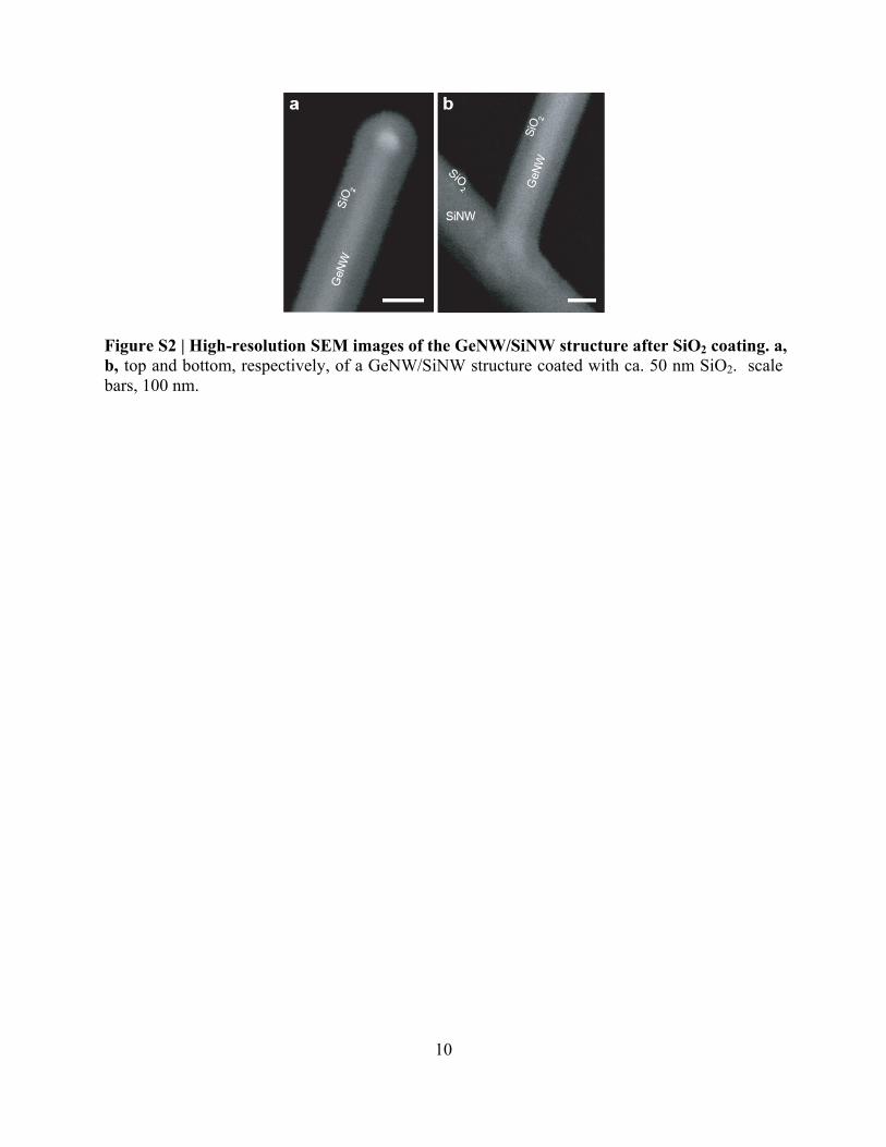
Figure S2 | High-resolution SEM images of the GeNW/SiNW structure after SiO2 coating. a, b, top and bottom, respectively, of a GeNW/SiNW structure coated with ca. 50 nm SiO2. scale bars, 100 nm.

11
Figure S3 | Solution access to BIT-FET. a, b, schematics of the BIT-FET before and after removing the GeNW, respectively. Inset of a, the cross-section view of a SiNW coated with conformal ALD SiO2, showing the half cylindrical configuration.
12
Figure S4 | BIT-FET device modelling and bandwidth analysis. a, conductance change versus time for a SiNW FET control device without nanotube (black trace) and the reconstructed intrinsic field-effect response of it (red trace). The Vwg pulse used had an amplitude, rise/fall time and duration of 100 mV, 0.1 ms, and 1 ms, respectively. b, equivalent circuit for intracellular recording by a BIT-FET device.
13
Figure S5 | Robustness of the BIT-FET device. SEM image of a BIT-FET device after five internalization/retraction cycles with intracellular recording achieved during each cycle. Some residue was observed on the top region of the nanotube at the completion of the multiple internalization/retraction experiment.
14
References
1. Patolsky, F., Zheng, G. & Lieber, C. M. Fabrication of silicon nanowire devices for
ultrasensitive, label-free, real-time detection of biological and chemical species. Nature
Prot. 4, 1711-1724 (2006).
2. Jiang, X. et al. Rational growth of branched nanowire heterostructures with synthetically-
encoded properties and function. Proc. Natl. Acad. Sci. USA 108, 12212-12216 (2011).
3. Hausmann, D., Becker, J., Wang, S., & Gordon, R. G. Rapid vapor deposition of highly
conformal silica nanolaminates. Science 298, 402-406 (2002).
4. Sze, S. M., & Ng, K. K. Physics of Semiconductor Devices, 3rd Edition (Wiley-
interscience, 2006).
5. Sadiku, M. N. O. Elements of Electromagnetics. 3rd edition. (Oxford University Press,
USA, 2000).
6. Hu, Y., Xiang, J. Liang, G., Yan, H., & Lieber, C. M. Sub-100 Nanometer Channel
Length Ge/Si Nanowire Transistors with Potential for 2 THz Switching Speed. Nano Lett.
8, 925-930 (2008).
7. Cohen-Karni, T., Timko, B. P., Weiss, L. E. & Lieber, C. M. Flexible electrical recording
from cells using nanowire transistor arrays. Proc. Natl. Acad. Sci. USA 106, 7309-7313
(2009).
8. Tian, B. et al. Three-dimensional, flexible nanoscale field-effect transistors as localized
bioprobes. Science 329, 831-834 (2010).