International Technology Roadmap for PV Results 2011
6
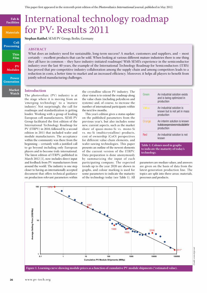
26 www.pv-tech.org Power Generation Market Watch Cell Processing Fab & Facilities Thin Film Materials PV Modules Introduction The photovoltaic (PV) industry is at the stage where it is moving from an ‘emerging technology’ to a ‘mature industry’. Not surprisingly, the call for roadmaps and standardization is getting louder. Working with a group of leading European cell manufacturers, SEMI PV Group facilitated the first edition of the International Technology Roadmap for PV (ITRPV) in 2010, followed by a second edition in 2011 that included wafer and module manufacturers. The acceptance within the community was there from the beginning – certainly with a justified call to go beyond including only European players and to become truly international. The latest edition of ITRPV, published in March 2012 [1], now includes direct input and feedback from PV manufacturers from around the world. The industry is one step closer to having an internationally accepted document that offers technical guidance on production-relevant parameters within the crystalline silicon PV industry. The clear vision is to extend the roadmap along the value chain (including polysilicon and systems) and, of course, to increase the number of international participants within the next few months. This year’s edition gives a status update on the published parameters from the previous year’s, but also includes some new, current aspects, such as the market share of quasi-mono-Si vs. mono-Si vs. mc-Si (multicrystalline) products, cost of ownership (CoO) perspectives for different value-chain elements, and wafer-sawing technologies. This paper presents an outline of the newest elements of the current version of the ITRPV. Data preparation is done anonymously by summarizing the input of each participating company. The expected trends up to the year 2020 are shown in graphs, and colour marking is used for some parameters to indicate the maturity of the technology today (see Table 1). All parameters are median values, and answers are given on the basis of data from the latest-generation production line. The topics are split into three areas: materials, processes and products. International technology roadmap for PV: Results 2011 Stephan Raithel, SEMI PV Group, Berlin, Germany ABSTRACT What does an industry need for sustainable, long-term success? A market, customers and suppliers, and – most certainly – excellent products that can be sold. When looking at various different mature industries there is one thing they all have in common – they have industry-initiated roadmaps! With SEMI’s experience in the semiconductor industry over the last 40 years, the example of the International Technology Roadmap for Semiconductors (ITRS) has proved that pre-competitive industry collaboration among the supply chain and among competitors leads to a reduction in costs, a better time to market and an increased efficiency. Moreover, it helps all players to benefit from jointly solved manufacturing challenges. Green An industrial solution exists and is being optimized in production Yellow An industrial solution is known but is not yet in mass production Orange An interim solution is known but is too expensive or not suitable for production Red An industrial solution is not known Table 1. Colours used in graphs to indicate the maturity of today’s technology. Credit: www.itrpv.net 1 10 100 0.1 1 10 100 1000 10000 100000 Average Selling Price (US$/Wp) Cumulative PV Module Shipments (MWp) 2011* 2006 1988 1996 1981 1976 Figure 1. Learning curve showing module prices as a function of cumulative PV module shipments (*estimated value). This paper first appeared in the sixteenth print edition of the Photovoltaics International journal, published in May 2012.
Transcript of International Technology Roadmap for PV Results 2011
26 w w w. p v - te ch . o rg
Power Generation
Market Watch
Cell Processing
Fab & Facilities
Thin Film
Materials
PV Modules
IntroductionThe photovoltaic (PV) industry is at the stage where it is moving from an ‘emerging technology ’ to a ‘mature industry’. Not surprisingly, the call for roadmaps and standardization is getting louder. Working with a group of leading European cell manufacturers, SEMI PV Group facilitated the first edition of the International Technology Roadmap for PV (ITRPV) in 2010, followed by a second edition in 2011 that included wafer and module manufacturers. The acceptance within the community was there from the beginning – certainly with a justified call to go beyond including only European players and to become truly international. The latest edition of ITRPV, published in March 2012 [1], now includes direct input and feedback from PV manufacturers from around the world. The industry is one step closer to having an internationally accepted document that offers technical guidance on production-relevant parameters within
the crystalline silicon PV industry. The clear vision is to extend the roadmap along the value chain (including polysilicon and systems) and, of course, to increase the number of international participants within the next few months.
This year’s edition gives a status update on the published parameters from the previous year’s, but also includes some new, current aspects, such as the market share of quasi-mono-Si vs. mono-Si vs. mc-Si (multicrystalline) products, cost of ownership (CoO) perspectives for different value-chain elements, and wafer-sawing technologies. This paper presents an outline of the newest elements of the current version of the ITRPV. Data preparation is done anonymously by summariz ing the input of each participating company. The expected trends up to the year 2020 are shown in graphs, and colour marking is used for some parameters to indicate the maturity of the technology today (see Table 1). All
parameters are median values, and answers are given on the basis of data from the latest-generation production line. The topics are split into three areas: materials, processes and products.
International technology roadmap for PV: Results 2011Stephan Raithel, SEMI PV Group, Berlin, Germany
AbStRActWhat does an industry need for sustainable, long-term success? A market, customers and suppliers, and – most certainly – excellent products that can be sold. When looking at various different mature industries there is one thing they all have in common – they have industry-initiated roadmaps! With SEMI’s experience in the semiconductor industry over the last 40 years, the example of the International Technology Roadmap for Semiconductors (ITRS) has proved that pre-competitive industry collaboration among the supply chain and among competitors leads to a reduction in costs, a better time to market and an increased efficiency. Moreover, it helps all players to benefit from jointly solved manufacturing challenges.
Green An industrial solution exists and is being optimized in production
Yellow An industrial solution is known but is not yet in mass production
Orange An interim solution is known but is too expensive or not suitable for production
Red An industrial solution is not known
table 1. colours used in graphs to indicate the maturity of today’s technology.
Cre
dit:
ww
w.itr
pv.n
et
1
10
100
0.1 1 10 100 1000 10000 100000
Aver
age
Selli
ng P
rice
(US$
/Wp)
Cumulative PV Module Shipments (MWp)
2011*
200619881996
1981
1976
Figure 1. Learning curve showing module prices as a function of cumulative PV module shipments (*estimated value).
This paper first appeared in the sixteenth print edition of the Photovoltaics International journal, published in May 2012.

28 w w w. p v - te ch . o rg
Fab & Facilities
“Only a combination of increased module performance
and considerably reduced manufacturing costs will
enable the PV industry to reach long-term competitiveness in
power generation.”cost reductionCost reduction in the production process has to result in price reductions. The chart in Fig. 1 shows the learning curve for PV modules and displays the average module selling price (in US$/Wp) as a function of modules sold over time (in MWp). When plotted on a log-log scale, the graph becomes approximately linear and reveals that, for every doubling in cumulative PV module shipments, the average selling price decreases by about 20%. Analyses in the last edition of ITRPV in 2011 [1] suggested that improvements in efficiency were important but contributed less significantly to the learning rate than reductions in production costs per piece. Only a combination of increased module performance and considerably reduced manufacturing costs will enable the PV industr y to reach long-term competitiveness in power generation.
cost elements and coO considerationsIn order to re duce costs the main cost factors have to be identified. The companies participating in the ITRPV have been using a standardized CoO
calculation model based on the following specifications: SEMI E35 (calculation), E10 (utilization) and E79 (efficiency). The main elements considere d are throughput, productivity, depreciation, f loor space, materials/consumables , utilities, waste disposal, labour and cost of yield loss. Assuming that throughput and productivity of state-of-the-art machines is very competitive, differentiation for each production step can be identified by an in-depth analysis of the specified main cost elements.
Fig. 2 shows the current situation of the relative distribution of cost elements for crystallization, wafering, and cell and mo dule pro duc tion according to an analysis of existing production lines among participating companies. Differences are clearly visible between the value-chain elements. In general, critical cost drivers are consumables (wear and spare parts) and materials that are non-silicon related. Expensive wear parts are crucibles (crystallization),
and slurry and wire (wafering). Critical materials, for instance, have so far been metallization pastes (cells), and the glass and backsheets (modules). Depreciation (capex) and floor space are cost drivers at all stages of the value chain. Depreciation in cell manufacturing, however, is not considered in our analysis, because of the higher frequency of investments in tool upgrades and line retrofits due to the speed of innovation in cell processing.Utilities (energy plus water) have a high share in crystallization, wafering and cell processing. Yield loss inf luences the cost in wafering, cell and module manufacturing. Because of recycling in the case of integrated crystallization and wafering lines, the cost of yield loss in wafering is significantly lower than in cell and module manufacturing. The share of labour costs strongly depends on the automation level of the lines considered, but is significant in all steps. This overview highlights that – besides the costs of materials, consumables and
Cre
dit:
ww
w.itr
pv.n
et
Figure 2. Relative distribution of cost elements in the different steps of the crystalline silicon PV value chain.
Cre
dit:
ww
w.itr
pv.n
et
Figure 3. Share of wafering based on diamond-wire technology vs. wafering based on slurry, for mono- and mc-Si (2010 = 100% slurry-based wafering).
utilities – the tool price, layout and user friendliness are important aspects in achieving further cost reductions along the PV value chain.
crystallization and waferingContinuous progress in standard poly production and in the development of alternative technologies is needed to enable further cost reduction without sacrificing silicon quality, as described in the SEMI Standards SEMI PV 17-0611 and SEMI PV 22-1011.
“A significant improvement in cost reduction in the wafering process is
expected by the introduction of
diamond-wire sawing.”
Cre
dit:
ww
w.itr
pv.n
et
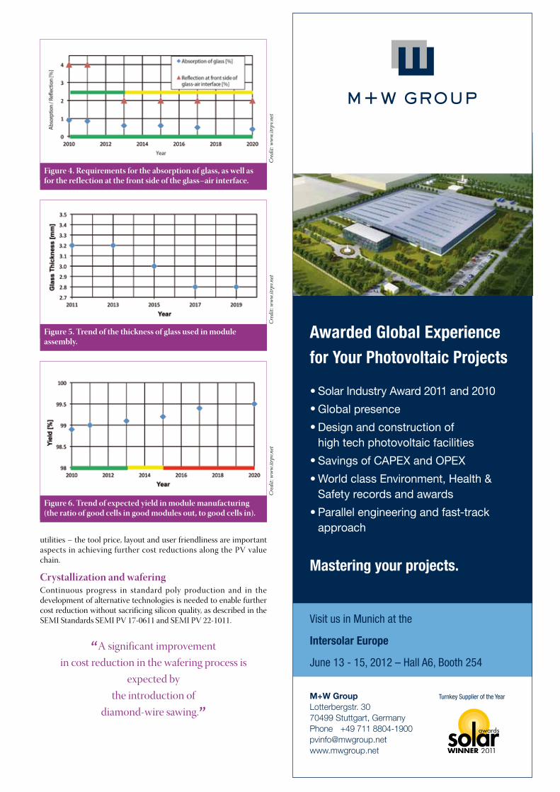
Figure 4. Requirements for the absorption of glass, as well as for the reflection at the front side of the glass–air interface.
Cre
dit:
ww
w.itr
pv.n
etC
redi
t: w
ww.
itrpv
.net
Figure 6. trend of expected yield in module manufacturing (the ratio of good cells in good modules out, to good cells in).
GER-MK-AM-120420-PVI 16th Edition_BUC.indd 1 23.04.2012 09:38:51
Figure 5. trend of the thickness of glass used in module assembly.

30 w w w. p v - te ch . o rg
Fab & Facilities
Further adjustment opportunities for cost reduction in crystallization and wafering are in the area of consumables, such as crucibles, graphite parts, slurry and sawing wires. It is assumed that prices will approach cost with these goods as well, and a price reduction of about 7% per year is possible. A significant improvement in cost reduction in the wafering process is expected by the introduction of diamond-wire sawing; Fig. 3 shows the projected share of this type of sawing in volume production. The roll-out of this technology requires synchronization with cell process development.
Module materialsBy looking at the module cost structure shown in the analysis of the different cost elements, it can be seen that consumables and materials are the main components which need performance improvements and price reductions. The reflectivity at the front side of the glass–air interface w il l b e re duce d from ty pical ly 4% to 2% by introducing anti-ref lection glass into the mainstream from 2013 onwards. The absorption of glass and encapsulant needs to be reduced in order to minimize the cell-to-module power loss. This is especially necessary for blue
light, because of the improved spectral response of solar cells in that region of the spectrum.
The reduction of the glass thickness is considered to be a potential cost reduction, as shown in Fig. 5. Thermal hardening of the glass seems to be a possible way of achieving the required temperature stability and stiffness for thicknesses down to 2.8mm. Only non-hardened or chemically hardened glass can be used at thicknesses below 2.8mm. Chemical hardening has to be performed in tanks with liquid molten salt , so thicknesses below 2.8mm are considered to be too difficult and too expensive to produce for larger formats like those used in modules. Even for thicknesses below 3mm, cells have to be very thin (< 80µm) in order to be flexible enough to follow the bending without breakage, otherwise stabilization elements or new back-cover materials that can carry the required mechanical load have to be introduced. Glass thickness reduction will therefore be challenging. Glass and backsheet foils have been identified as being an important cost driver in module building. Besides glass and backsheet foils, the other consumables are frames, encapsulants , interconnections and junction boxes, which have approximately equal contributions in the distribution of costs. All materials should therefore contr ibute e qual ly to the ongoing reduction in module manufacturing costs.
Copper is expected to remain the chief interconnection material in the coming years. The junction box is the electrical interface of the module, and the material used for mounting it to the back side of the module is still expected to be silicone. Starting in 2015, it is anticipated that the actual internal electrical interconnections will change from being soldered/clamped to being welded. All materials used in the module contribute to the reliability of the PV installation. Reliability considerations will become important in developing new standards and guidelines and may be considered in future ITRPV issues as well.
Process – manufacturingThe trend of expected yield in module manufacturing is shown in Fig . 6 . Continuous improvements are implied, despite ongoing reductions in wafer thickness and implementations of new wafer-sawing technologies. In order to process cells of thicknesses less than 150µm with greater than 99.3% yield from 2015 onwards, a dramatically improved interconnection technology is needed, in addition to stress-relieving supporting structures. By 2015 at the latest, lead-free soldering must be implemented into mass production at the same time as the introduction of lead-free cell metallization technologies.
Cre
dit:
ww
w.itr
pv.n
et
Figure 7. Expected trend of wafer total thickness variation (ttV).
Cre
dit:
ww
w.itr
pv.n
et
Figure 8. Kerf-loss reduction trend.
Cre
dit:
ww
w.itr
pv.n
et
Figure 9. Expected trend of the module-to-cell power ratio.

Fab & Facilities
Process – technologyBesides production parameters, cell efficiency is also expected to improve; the process parameters that are necessary for achieving this improvement will be discussed next. One essential requirement for thinner solar cells, reflecting the needs from a cell-production point of view, is the reduction of total thickness variation (TTV): the TTV of wafers should not exceed 10% of the wafer thickness without any additional cost (see Fig. 7).
Another challenging parameter is kerf loss. Along with wafer-thickness reduction, kerf loss must also be decreased accordingly, to achieve a significant re duction in s i l icon consumption.
You Can Be That Missing Piece!PV Directory offers you the fastest and most cost-effective way to generate new business opportunities in the solar supply chain. It offers an affordable alternative or addition to your advertising and PR campaign by providing company- and product-specific information to business professionals in the solar industry. The online directory also attracts businesses that are looking to enter the high growth solar industry.
Benefits at a Glance f Put an always up-to-date summary of your company in front of
key industry decision makers who are looking to source suppliers.
f Showcase your specific products and solutions in words and images.
f Make your services searchable against multiple product and geographical criteria.
f Exploit the Photovoltaics International branding and authoritative image to maximise the exposure for your company.
f Boost traffic to your corporate website and improve your SEO efforts.
The leading online sourcing directory for the solar industry – find the perfect fit for your supply chain.
If you’re not in front of them, then who is?
Reach over 180,000 visitors and 620,000 pageviews per month as part of www.PV-tech.org!Benefit from the most authoritative PV website worldwide and channel real business to your website!
Please contact Ben Irving [email protected] or alternatively, dial: +44 (0)20 7871 0123
pvdirectory_halfpage_horizontal_150x210.indd 1 18/11/2011 14:17:33
Cre
dit:
ww
w.itr
pv.n
et
Figure 10. Expected market share of mc-Si, mono-like Si and mono-Si materials.
Cre
dit:
ww
w.itr
pv.n
et
Figure 11. (a) Stabilized cell-efficiency trend curve. (b) Module-power trend curve.
(a) (b)

32 w w w. p v - te ch . o rg
Fab & Facilities
Additional reductions are expected by the introduction of diamond-wire sawing processes (Fig. 8).
It is crucial to get as much power out of the assembled solar cells as possible. A go o d parameter expressing this achievement is the module-to-cell power ratio, defined as: module power/(cell power × number of cells). As shown in Fig. 9, for 2011 this ratio was around 98% for multicrystalline silicon cell technology and about 96% for monocrystalline silicon cell technology. In 2013 the power ratio will show an improvement of +1% absolute as a result of the introduction of anti-reflective glass. The launch of new interconnection and encapsulation technologies (for thinner wafers, back-contacted cells, etc.) from 2015 onwards will result in a second improvement step of about +1.0% absolute.
ProductsMono-like silicon material is an emerging new technolog y that util izes mc-Si crystallization equipment to grow silicon ingots which have larger volume fractions than mc-Si but with monocrystalline properties. As this material is well suited for high-efficiency cells, an increasing market share for mono-like silicon material is expected within the coming years, as shown in Fig. 10. The market share of n-type mono-Si wafers is expected to increase over the next few years, starting at around 10% in 2012 and increasing to 50% in 2020. The roadmap predicts a much lower market share for n-type mc-Si wafers.
Over the next few years, the efficiency of p-type silicon solar cells will continue to improve. Fig. 11(a) shows the expected
trend of average stabilized efficiencies for mc-Si, mono-like Si and mono-Si solar cells with double-sided contacts, manufactured in state-of-the-art mass production lines. Because of the improved material quality of mono-like sil icon, the difference between p-type mono-Si and mono-like material is likely to decrease in the coming years. Moreover, n-type mono-Si will show significantly higher efficiencies.
“The market share of n-type mono-Si wafers is expected to
increase over the next few years, starting at around 10% in 2012
and increasing to 50% in 2020.”The chart in Fig. 11(b) illustrates the
corresponding development of module power, taking into account that, starting in 2013, there will be a transition in mono-Si wafers from a semi-square to a full-square format. Cell-to-module power losses were assumed on the basis of the values mentioned in the full edition of the latest roadmap [1] for the different material types. For mono-like silicon, the same module-to-cell power ratio as for mono-silicon was used.
conclusionThe data shown here (extracted from the latest ITRPV edition) was collected in 2011 from leading international PV manufacturers along the c-Si value chain. A yearly update of this information is planned, and the next edition of the ITRPV, based on
data collected in 2012, will be published in March 2013. Topics such as wafer thickness require cooperation between tool suppliers, cell manufacturers and other players along the value chain. The current issue of this document, as well as information about how to get involved in the roadmap activities, can be downloaded from the ITRPV website [1].
Reference[1] International Technology Roadmap
for PV (ITRPV), March 2012 [details available online at http://www.itrpv.net].
About the AuthorS t e p h a n R a i t h e l i s currently the director of PV Europe within SEMI PV Group, and the key SEMI spokesperson for the PV community in Europe. One
of his main functions is the facilitation of the International Technology Roadmap for PV, ensuring the data collection and data protection, antitrust environment, and recruitment of new participants. Stephan is concurrently the managing director of the Berlin branch office of SEMI.
EnquiriesStephan RaithelDirector PV Europe, SEMI PV GroupHelmholtzstrasse 2–9House D / 3rd FloorD-10587 BerlinGermany
Email: [email protected]