
INTERNATIONAL JOURNAL OF PURE AND APPLIED … - 435.pdf · INTERNATIONAL JOURNAL OF PURE AND ......
14
Research Article Impact Factor: 4.226 ISSN: 2319-507X Betty George, IJPRET, 2015; Volume 4 (1): 33-46 IJPRET Available Online at www.ijpret.com 33 INTERNATIONAL JOURNAL OF PURE AND APPLIED RESEARCH IN ENGINEERING AND TECHNOLOGY A PATH FOR HORIZING YOUR INNOVATIVE WORK TEST STATION FOR PIC MICROCONTROLLER USING FPGA BETTY GEORGE 1 , TINA RAJA 2 1. PG Student [Applied Electronics], Dept. of ECE, MG University College of Engineering, Thodupuzha, Kerala, India. 2. Scientist/Engineer "SE", QDAC/QRAG/SR/ VSSC, Trivandrum, Kerala, India. Accepted Date: 25/08/2015; Published Date: 01/09/2015 Abstract: - The PIC microcontroller’s are used in various applications, from control logic to fully integrated systems involving USB, Ethernet and LCD. It is of high importance that the PIC’s functionality is tested before realizing into applicati on circuit. In industries, VLSI testers are used for testing purpose. Processor per pin architecture is employed in VLSI testers to serve the purpose. These systems are very complex, large and expensive. The proposed system has a standalone feature and mainly focuses on testing of the various modules in PIC18F6520. The programmer used to program the various modules of microcontroller is Microchip MPLAB. FPGA is the main controller of the proposed system. The implementation of FPGA is done using HDL in ModelSim platform and synthesis in Xilinx platform. Microsoft Visual Basic is used for the graphical user interface. Keywords: PIC Microcontroller, FPGA Corresponding Author: MR. BETTY GEORGE Access Online On: www.ijpret.com How to Cite This Article: Betty George, IJPRET, 2015; Volume 4 (1): 33-46 PAPER-QR CODE
Transcript of INTERNATIONAL JOURNAL OF PURE AND APPLIED … - 435.pdf · INTERNATIONAL JOURNAL OF PURE AND ......

Research Article Impact Factor: 4.226 ISSN: 2319-507X Betty George, IJPRET, 2015; Volume 4 (1): 33-46 IJPRET
Available Online at www.ijpret.com
33
INTERNATIONAL JOURNAL OF PURE AND APPLIED RESEARCH IN ENGINEERING AND
TECHNOLOGY A PATH FOR HORIZING YOUR INNOVATIVE WORK
TEST STATION FOR PIC MICROCONTROLLER USING FPGA
BETTY GEORGE1, TINA RAJA2 1. PG Student [Applied Electronics], Dept. of ECE, MG University College of Engineering, Thodupuzha, Kerala, India.
2. Scientist/Engineer "SE", QDAC/QRAG/SR/ VSSC, Trivandrum, Kerala, India.
Accepted Date: 25/08/2015; Published Date: 01/09/2015
\
Abstract: - The PIC microcontroller’s are used in various applications, from control logic to fully integrated systems involving USB, Ethernet and LCD. It is of high importance that the PIC’s functionality is tested before realizing into application circuit. In industries, VLSI testers are used for testing purpose. Processor per pin architecture is employed in VLSI testers to serve the purpose. These systems are very complex, large and expensive. The proposed system has a standalone feature and mainly focuses on testing of the various modules in PIC18F6520. The programmer used to program the various modules of microcontroller is Microchip MPLAB. FPGA is the main controller of the proposed system. The implementation of FPGA is done using HDL in ModelSim platform and synthesis in Xilinx platform. Microsoft Visual Basic is used for the graphical user interface.
Keywords: PIC Microcontroller, FPGA
Corresponding Author: MR. BETTY GEORGE
Access Online On:
www.ijpret.com
How to Cite This Article:
Betty George, IJPRET, 2015; Volume 4 (1): 33-46
PAPER-QR CODE

Research Article Impact Factor: 4.226 ISSN: 2319-507X Betty George, IJPRET, 2015; Volume 4 (1): 33-46 IJPRET
Available Online at www.ijpret.com
34
INTRODUCTION
Microcontroller is a small computer on a single integrated circuit containing a processor core,
memory, and programmable input/output peripherals. Program memory is in the form
of Ferroelectric RAM, NOR flash or OTP ROM is also often included on chip. Peripheral Interface
Controller (PIC) is a family of microcontrollers made by Microchip Technology. To ensure the
working of the device, it is required to test the device to its full functionality.
Device under test (DUT) is PIC18F6520 microcontroller. It is a 64 pin, flash memory
incorporated microcontroller. Communication with the PIC is made possible using the SPI,
UART, I2C protocols etc. There are 5 timers present that work as 8 bit or 16 bit timers or
counters. Capture/Compare/PWM (CCP) modules are also present in the specified PIC. The data
memory is 2048 Bytes and the data EPROM is 1024 Bytes. The operating frequency of the PIC is
40 Mhz and there is 17 interrupt sources.PIC 18F6520 uses 16 bit wide instructions and 8 bit
wide data path.
In general, testing at manufacture side is carried out using VLSI tester. The test programs are
developed in assembly language for testing the different modules of PIC 18F6520. For each
module the expected response obtained from the simulator is stored in tester memory. The
tester captures the response and compares the observed response with the expected response
stored in the vector memory of the tester and gives PASS/FAIL.
The proposed system is meant to test the various modules of PIC microcontroller like ALU, byte
oriented file register operations, byte oriented file register operations, literal operation, Timer
modules, CCP modules, UART module, SPI of MSSP module and memory. For this FPGA is used
as a main controller. In FPGA, the various protocols to test the microcontroller parallel interface
to SRAM and RS232 interface to PC are implemented. This is done in VHDL using ModelSim and
implemented in Xilinx. The PIC is programmed using MPLab from Microchip. The basic structure
diagram for testing of a PIC microcontroller is as Fig.1.
Fig.1 Basic Structure Diagram

Research Article Impact Factor: 4.226 ISSN: 2319-507X Betty George, IJPRET, 2015; Volume 4 (1): 33-46 IJPRET
Available Online at www.ijpret.com
35
The upper hand of the proposed system when compared to other testing method is its stand
alone feature. The interfaces implemented in FPGA could be used for the communication
between other devices such as test station and FPGA, as they are standard communication
protocols. SPI and UART protocols are implemented and tested in the proposed system.
Selectable frequency operation for the above mentioned communication protocols make it apt
for the testing of microcontrollers. The memory implemented is employed for the storage of
data captured from PIC.
SOFTWARE ENVIRONMENT
The implementation and synthesis of the main controller is done in ModelSim and Xilinx
software platform. ModelSim is an HDL simulation environment by Mentor Graphics. It is used
for the simulation of hardware description languages. The four basic flow in development of
HDL design involves creating the working library, compiling of design, loading the simulator
with design and running the simulation and debugging of results. Xilinx ISE is the software
platform used for the programming of FPGA. Compiling of designs, retrieving RTL schematics,
timing analysis etc is done using Xilinx ISE. MPLab from Microchip Technology helps in
programming PIC as the specific PIC under consideration does not have an external memory
interface. Microsoft Visual Basic forms the front end of the proposed system. Graphical user
interface containing the test result is displayed in VB.
HDL DEVELEOPMENT OF INTERFACES
UART
UART is an asynchronous serial communication protocol which accomplishes communication
between slow and fast peripherals. Low cost and short distance characteristics of the protocol
make it ideal for many applications. An UART module consists of a transmitter, baud rate
generator and a receiver. A parallel to serial and serial to parallel conversion of data takes place
in transmitter and receiver end respectively.
Transmitter module consists of hold register and shift register. Hold register takes in data from
the memory and the data is moved into the shift register where the start bit, stop bit and the
parity bit is added and shifted out in a serial manner. The structure diagram of the UART
module is given in Fig. 2. In the proposed system the data to be transmitted is taken from the
memory implemented.

Research Article Impact Factor: 4.226 ISSN: 2319-507X Betty George, IJPRET, 2015; Volume 4 (1): 33-46 IJPRET
Available Online at www.ijpret.com
36
Fig.2 Structure diagram of UART.
Receiver module hold registers serves the purpose of holding data and shift registers are used
for the shifting in of data. The start bit and top bit are checked for and not stored onto the
memory. The memory implemented is used for the storage of data received.
Baud rate generator serves the purpose of generating sampling signals with frequency sixteen
times that of the designated baud rate. In the proposed system, the baud rate is selectable.
SPI
SPI is s synchronous communication protocol. The protocol supports master and slave
communication, specifically a single master. The clock signal for the communication is
generated by the master is supplied to all slaves associated. The SPI is selectable in the case of
a PIC microcontroller and so the SPI implemented onto the FPGA also possess a selectable
frequency of operation.
As communication initiated, the master selects the slave to which the data to be exchanged by
the use of SS signal. SS signal is an active low signal. SPI protocol is a full duplex communication
where data is transferred between the master as well as the slave. Data is send to slave using
the MOSI line bit by bit and MISO line brings back the data from the slave bit by bit on every
clock cycle SCLK. When an eighth bit is sent out of the shift register of the SPI master, the eighth
bit of SPI slave is moved onto the first position of the master shift register. Thus when eighth
executive cycles are over, the data in the master and slave shift registers get exchanged. The
master as well as the slave acts as transmitter and receiver at the same time. The basic
structure diagram of SPI is as in Fig.3.

Research Article Impact Factor: 4.226 ISSN: 2319-507X Betty George, IJPRET, 2015; Volume 4 (1): 33-46 IJPRET
Available Online at www.ijpret.com
37
Fig.3 Structure diagram of SPI.
Memory
Memory is implemented in order to collect data that are captured from PIC for the comparison
purpose. The memory implemented for this particular proposed system is an array type
consisting of 256 locations that are 8 bit wide.
Parallel Ports
Parallel ports are implemented to make the communication possible through the parallel ports.
The parallel port is designed on the concept of capturing data from parallel ports of PIC.
TEST VECTOR DEVELOPMENT OF PIC
Test vector development of PIC is done. The PIC modules tested for are the byte oriented file
register operations, bit oriented file register operations, literal operations, CCP modules, Timers
modules, UART, SPI and memory. The DUT do not possess an external memory interface and
thus the programming is done using MPLAB from Microchip.
Bit And Byte Oriented File Register Operations
The bit and byte oriented file register operations include ADDWF, INCF, COMF, MOVF, BCF, BSF,
BC etc. Programs that test the correctness of the file operations are written. The output
obtained from PIC is compared to the ideal values. Similar values indicate the operations
perform as expected.

Research Article Impact Factor: 4.226 ISSN: 2319-507X Betty George, IJPRET, 2015; Volume 4 (1): 33-46 IJPRET
Available Online at www.ijpret.com
38
CCP Modules
CAPTURE/COMPARE/PWM modules are 5 in number for PIC 18F6520. Each module contains a
16-bit register, which can operate as a 16-bit Capture register, a 16-bit Compare register or a
Pulse Width Modulation (PWM) Master/Slave Duty Cycle register. In Capture mode,
CCPR1H:CCPR1L captures the 16-bit value of the TMR1 or TMR3 registers when an event occurs
on pin RC2/CCP1. In Compare mode, the 16-bit CCPR1 register value is constantly compared
against either the TMR1 register pair value or the TMR3 register pair value. If a match occurs,
an event occurs. Event is represented by change in value on the corresponding pin. In Pulse
Width Modulation (PWM) mode, the corresponding pin produces up to a 10-bit resolution
PWM output. Programs are written to PIC fulfilling the above conditions.
Timer Modules
PIC 18F6520 has 5 timer modules named as Timer 0, Timer 1, Timer 2, Timer 3 and Timer 4.
Timers act as software selectable 8/16 bit timer or counter. There are several registers defined
in PIC architecture that control the working of these timers or counters. Programming is done
for each of the timer modules and testing is carried out.
UART
Universal Asynchronous Receiver Transmitter also called Serial Communications Interface (SCI)
is one among the serial communication available in specified PIC. Each device has two UART
modules which could be configured independently. Both full duplex communication as well as
half duplex communication is made possible using UART module. Full duplex communication is
made use for the communication of peripheral devices such as personal computer etc while
half duplex communication is accomplished with peripheral devices such as A/D OR D/A
circuits. Transmitter and receiver control registers are used to select the various conditions.
Baud Rate Generator (BRG) is used to set the desired baud rate. Baud rate is set in the SPBRG
register. A shift register forms the important part of both the transmitter and receiver block.
SPI
Serial Peripheral Interface is one among the master synchronous serial port (MSSP) module. SPI
module works in either master mode or in slave mode. The master and slave could possibly be
processors. The master device initiates the communication. The clock signal required is
generated by the master and slave is supplied with the clock from the master. It is a full duplex
communication system where both the master and slave is sending and receiving data
simultaneously.

Research Article Impact Factor: 4.226 ISSN: 2319-507X Betty George, IJPRET, 2015; Volume 4 (1): 33-46 IJPRET
Available Online at www.ijpret.com
39
GRAPHICAL USER INTERFACE
Graphical user interface is formed in Microsoft Visual Basic platform. The values are captured
by the test station via RS 232 protocol. The captured value is compared against the actual value
and a PASS/FAIL is produced in the test station.
RESULTS
HDL implementation of interfaces is done in ModelSim platform. UART transmitter is given in
Fig.4. Transmitter acts as a parallel to serial converter that takes in data from the memory in a
parallel manner and converts the data into serial one and sends it out. State machines are used
to realize the working and functionality of transmitter. There are 11 transmitter states in a
transmitter state machine. Each state lasts for the defined baud clock cycle.
Fig.4 Transmitter
UART receiver’s working and functionality is realized using state machines. The receiver state
machine also consists of 11 states. A start bit is polled for and when a bit is received, it is
checked so as to ensure that the received bit is a start bit. Then after a baud clock cycle, the
next bit is received and stored until the eighth bit is stored. The stop bit is checked. This process
continues. Receiver implantation is given in Fig.5.
Fig.5 Receiver
The SPI implementation of SPI is described in Fig.6. The SPI module given shifts out data in a
serial manner at every clock cycle. After eight consecutive clock cycles, data are exchanged

Research Article Impact Factor: 4.226 ISSN: 2319-507X Betty George, IJPRET, 2015; Volume 4 (1): 33-46 IJPRET
Available Online at www.ijpret.com
40
between the slave and the master. A signal SS defines the working frequency of the device. For
SS=”00”, the clock frequency selected is Fosc/4, for SS=”01” clock frequency is Fosc/16 and for
SS=”11”, clock frequency is Fosc/64.
Fig.6 SPI
Memory is also implemented so that the values are stored temporarily. Memory read and
memory write signals are defined. The writing onto the memory is done if and only if the
memory has free space similarly; reading from the memory is only possible when the memory
is occupied. These two conditions are accomplished using full and empty signals. Fig.7 is the
memory implementation.
Fig.7 Memory
Synthesis is done using Xilinx ISE 10.4. The device used is Spartan3xc3s400. The design
summary report in table 1 shows the utilization of slices flip flops etc.
Logic Utilization Used Available Utilization
Number of slices 1494 3584 41% Number of slice flip flop’s 599 7168 8% Number of 4 input LUT’s 2841 7168 39% Number of bonded IOB’s 19 141 13% Number of GCLK’s 2 8 25%
Table 1 Device Utilization

Research Article Impact Factor: 4.226 ISSN: 2319-507X Betty George, IJPRET, 2015; Volume 4 (1): 33-46 IJPRET
Available Online at www.ijpret.com
41
RTL schematic generated for the Xilinx synthesis is as in Fig.8
Fig. 8 RTL Schematic
Test vector development of the PIC is done. The CCP modules are checked for. The various
registers used for capture mode are T3CON, T1CON, PIE1 etc. The value in the timer module is
captured when an event occurs. The event could either b a falling edge or rising edge etc at the
corresponding pin. Fig.9 defines the test vector development for capture mode.
Fig.9 Capture
Compare mode is defined by an occurrence of an event at the specified pin when the timer
value and the CCP register values are equal. An interrupt is generated. Fig.10 defines the test
vector development for capture mode.

Research Article Impact Factor: 4.226 ISSN: 2319-507X Betty George, IJPRET, 2015; Volume 4 (1): 33-46 IJPRET
Available Online at www.ijpret.com
42
Fig.10 Compare
Timer modules are five in number and their operation as 8/16 bit timer or counter is validated.
Fig 11 gives the test vector development for Timer 0. Control registers are used to set the
device Timer 0. When an overflow occurs, an interrupt is generated.
Fig.11 Timer 0
Timer 1 acts as 16 bit counter. It counts up to 16 bit. Interrupt is generated when an overflow
FFFFh to 0000h occurs. A value is output through the port so that the validation of the module
is done. . Fig 12 gives the test vector development for Timer 1.

Research Article Impact Factor: 4.226 ISSN: 2319-507X Betty George, IJPRET, 2015; Volume 4 (1): 33-46 IJPRET
Available Online at www.ijpret.com
43
Fig.12 Timer 1
Timer 2 is an 8-bit timer. An 8 bit period register is also associated with the Timer 2 module. It is
both readable and writable. An interrupt occur when the value of Timer 2 and the period
register matches. It is also used as a time base for PWM module. . Fig 13 gives the test vector
development for Timer 2.
Fig.13 Timer 2
Timer 3 is 16-bit timer/counter. Internal or external clock select is available. Interrupt is
generated when an overflow FFFFh to 0000h occurs. Timer 3 module is both readable and
writable. Timer 3 acts as a timer, a synchronous counter or an asynchronous counter. Fig 14
gives the test vector development for Timer 3.

Research Article Impact Factor: 4.226 ISSN: 2319-507X Betty George, IJPRET, 2015; Volume 4 (1): 33-46 IJPRET
Available Online at www.ijpret.com
44
Fig.14 Timer 3
Timer 4 acts as 8-bit timer. The Timer is both readable and writable. Programmable prescaler
and postscaler is present. Interrupt is generated when a match occurs between the values of
timer register and period register. Fig 15 gives the test vector development for Timer 4.
Fig.15 Timer 4
Test vector generation of UART is also done, in Fig 16. Asynchronous full duplex mode
transmission is explained. Baud rate is set and the corresponding value is given in the baud rate
register. High speed and low speed operation is possible. The transmitter control register
defines the working. In the asynchronous mode UART uses N Non-Return-to- Zero (NRZ) format
(one Start bit, eight or nine data bits and one Stop bit).
Research Article Impact Factor: 4.226 ISSN: 2319-507X Betty George, IJPRET, 2015; Volume 4 (1): 33-46 IJPRET
Available Online at www.ijpret.com
45
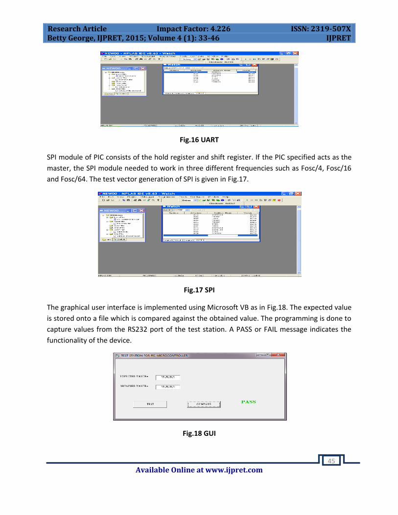
Fig.16 UART
SPI module of PIC consists of the hold register and shift register. If the PIC specified acts as the
master, the SPI module needed to work in three different frequencies such as Fosc/4, Fosc/16
and Fosc/64. The test vector generation of SPI is given in Fig.17.
Fig.17 SPI
The graphical user interface is implemented using Microsoft VB as in Fig.18. The expected value
is stored onto a file which is compared against the obtained value. The programming is done to
capture values from the RS232 port of the test station. A PASS or FAIL message indicates the
functionality of the device.
Fig.18 GUI

Research Article Impact Factor: 4.226 ISSN: 2319-507X Betty George, IJPRET, 2015; Volume 4 (1): 33-46 IJPRET
Available Online at www.ijpret.com
46
CONCLUSION
PIC is used in wide range of applications such as commercial, industrial and automotive
applications. It is important that the device is tested prior to wiring in the application circuit.
PIC microcontroller 18F6520 is tested for its precision using a standalone system. The main
controller used is an FPGA onto which the communication protocols are implemented. FPGA
device could be used for the communication between test station and a peripheral device that
has any one of the communication protocol implemented on the controller. It also acts as a
temporary storage of data. The graphical user interface indicates whether the PIC has passed or
failed to meet the need.
REFERENCES
1. Dr G.B.Wakle, I. Aggarwal and S. Gaba, “Synthesis and Implementation of UART using VHDL
Codes”, International Symposium on Computer, Consumer and Control, pp.1-3, June 2012.
2. Y. Wang and K. Song, “A New Approach to Realize UART,” in Electronic and Mechanical
Engineering and Information Technology (EMEIT), International Conference, vol. 5, pp. 2749 –
2752, 2011.
3. T.P.Blessington, B.B.Murthy, G.V.Ganesh and T.S.R Prasad, “Optimal Implementation of
UART-SPI Interface in SOC”, Devices, Circuits and Systems (ICDCS), International Conference,
pp.673-67, 2012.
4. S. Yu, L. Yi, W. Chen, and Z. Wen, “Implementation of a Multichannel UART Controller Based
on FIFO Technique and FPGA,” in Industrial Electronics and Applications.ICIEA,2nd IEEE
Conference, pp. 2633 –2638, 2007.
5. Motorola Inc., “SPI Block Guide V03.06,” February 2003.
6. XU L Y, "Realization of UART Communication Based on FPGA” Microcomputer Information,
vol. 23(35), pp. 218-219, 2007.