INTERNATIONAL JOURNAL OF PURE AND APPLIED … - 420.pdf · · 2015-08-08using Tanner EDA tool....
9
Research Article Impact Factor: 4.226 ISSN: 2319-507X R Siva Kumar, IJPRET, 2015; Volume 3 (12): 191-199 IJPRET Available Online at www.ijpret.com 191 INTERNATIONAL JOURNAL OF PURE AND APPLIED RESEARCH IN ENGINEERING AND TECHNOLOGY A PATH FOR HORIZING YOUR INNOVATIVE WORK DESIGN OF A LOW-POWER EFFICIENT DOUBLE EDGE TRIGGER FLIP FLOP R SIVA KUMAR 1 , T SRINIVASA PADMAJA 2 1. M. Tech Student, Embedded systems, Department of ECE, Siddhartha Institute of Engineering & Technology, A.P., India, 2. Assistant Professor, Department of ECE, Siddhartha Institute of Engineering & Technology, A.P., India, Accepted Date: 24/07/2015; Published Date: 01/08/2015 Abstract: - The data signal changes in Double-edge triggered Flip-Flops on both the rising and falling clock edges. Thus, results in low clock swing and it leads to lower power consumption and the data throughout are preserved. The leakage current has become a most dominant problem in VLSI system design, because it leads to more power consumption. Some of the methods have been presented in this paper to control the leakage current. The proposed design successfully solves the long discharging path problem in conventional explicit type pulse-triggered FF (P-FF) designs and achieves better speed and power performance. Also, DDFF and P-FF are compared with other state-of-the-art designs and DD-FF design is implemented in a 4-b ring counter. The performance improvements indicate that the proposed designs are well suited for modern high-performance designs where power dissipation and latching overhead are of major concern. The proposed circuit is simulated using Tanner EDA tool. The simulations are carried out by applying T-SPICE software. The number of clock transistors decrease which in turn results in lower leakage current, hence the power consumption reduces. Keywords: P-FF, DDFF, Ring Counter Corresponding Author: MR. R. SIVA KUMAR Access Online On: www.ijpret.com How to Cite This Article: R. Siva Kumar, IJPRET, 2015; Volume 3 (12): 191-199 PAPER-QR CODE
Transcript of INTERNATIONAL JOURNAL OF PURE AND APPLIED … - 420.pdf · · 2015-08-08using Tanner EDA tool....

Research Article Impact Factor: 4.226 ISSN: 2319-507X R Siva Kumar, IJPRET, 2015; Volume 3 (12): 191-199 IJPRET
Available Online at www.ijpret.com
191
INTERNATIONAL JOURNAL OF PURE AND APPLIED RESEARCH IN ENGINEERING AND
TECHNOLOGY A PATH FOR HORIZING YOUR INNOVATIVE WORK
DESIGN OF A LOW-POWER EFFICIENT DOUBLE EDGE TRIGGER FLIP FLOP
R SIVA KUMAR1, T SRINIVASA PADMAJA2
1. M. Tech Student, Embedded systems, Department of ECE, Siddhartha Institute of Engineering & Technology, A.P., India,
2. Assistant Professor, Department of ECE, Siddhartha Institute of Engineering & Technology, A.P., India,
Accepted Date: 24/07/2015; Published Date: 01/08/2015
\
Abstract: - The data signal changes in Double-edge triggered Flip-Flops on both the rising and falling clock edges. Thus, results in low clock swing and it leads to lower power consumption and the data throughout are preserved. The leakage current has become a most dominant problem in VLSI system design, because it leads to more power consumption. Some of the methods have been presented in this paper to control the leakage current. The proposed design successfully solves the long discharging path problem in conventional explicit type pulse-triggered FF (P-FF) designs and achieves better speed and power performance. Also, DDFF and P-FF are compared with other state-of-the-art designs and DD-FF design is implemented in a 4-b ring counter. The performance improvements indicate that the proposed designs are well suited for modern high-performance designs where power dissipation and latching overhead are of major concern. The proposed circuit is simulated using Tanner EDA tool. The simulations are carried out by applying T-SPICE software. The number of clock transistors decrease which in turn results in lower leakage current, hence the power consumption reduces.
Keywords: P-FF, DDFF, Ring Counter
Corresponding Author: MR. R. SIVA KUMAR
Access Online On:
www.ijpret.com
How to Cite This Article:
R. Siva Kumar, IJPRET, 2015; Volume 3 (12): 191-199
PAPER-QR CODE

Research Article Impact Factor: 4.226 ISSN: 2319-507X R Siva Kumar, IJPRET, 2015; Volume 3 (12): 191-199 IJPRET
Available Online at www.ijpret.com
192
INTRODUCTION
Most of the Flip-flops (FFs) are the memory storage elements extensively used in many digital
designs. In particular, digital designs consisting of a intensive pipelining techniques and employ
many FF-rich modules such as register file, shift register, and counters. It is also calculated that
the power consumption of the clock system, which consists of clock distribution networks and
storage elements, which consumes 50% of the total system power. FFs thus contribute a major
portion of the chip area and power consumption to the overall system design.
The power dissipation is an important factor for the low power applications. The power
optimization techniques are used at different levels of a digital design. The optimization at the
logic level is one of the most necessary tasks for minimizing the power consumption. The
latches and flip flops are viewed as the critical logic components for the effectiveness of the
digital circuits. They are widely used in the memory design, test applications and pipelines
implementations. Since the power consumption depends on several parameters, different
methods have been applied to reduce each of them. The processing speed of the system is
doubled, if both clock edges have been used or the processing speed is preserved, if the circuit
frequency becomes half. As the frequency becomes half it implies that the dynamic power of
flip-flop and clock distribution network are half. The circuit uses flip-flop with both clock edges.
Figure 1: Pulse Triggered Flip flop
In this design the dynamic power consumption and the leakage current have been decreased
and components related to the leakage current are considered. Fig. 1depicts the proposed
static flip-flop circuit with double triggered pulse edges.

Research Article Impact Factor: 4.226 ISSN: 2319-507X R Siva Kumar, IJPRET, 2015; Volume 3 (12): 191-199 IJPRET
Available Online at www.ijpret.com
193
Figure 2: Explicit Pulse triggered FF design
Pulse-triggered FF (P-FF), because of its single-latch structure, is more popular than the
transmission gate (TG) and master–slave based FFs in higher speed applications. Apart from the
speed advantage, its circuit simplicity lowers the power consumption of the clock tree system.
A P-FF consists of a pulse generator for strobe signals and a latch is for data storage. If the
triggering pulses are narrow, the latch acts like an edge-triggered FF. Since only one latch, as
opposed to two in the conventional master–slave configuration, is needed, a P-FF is simpler in
circuit complexity.
In this existing P-FF the load capacitance has been reduced and the ground bounce noise to be
reduced. The pass transistor has been to be added in the circuit to control by the clock pulse
signal to reduce the switching power. The pull up and the pull down transistor are also used to
enable the clock pulses for the input of the data and the clock. This scheme actually improves
the logic “0” to logic “1” delay and thus reduces the comparison between the rise time and the
fall time delays. By reducing the time and the switching delay it automatically reduces the
switching power in the circuit. The pulse-triggered means that data are entered into the flip-
flop on the rising edge of the clock pulse, but the output does not reflect the input state until
the falling edge of the clock pulse. And these kind of flip-flops are sensitive to any change of the
input levels during the clock pulse is still HIGH, the inputs must be set up prior to the clock
pulse's rising edge and must not be changed before the falling edge.

Research Article Impact Factor: 4.226 ISSN: 2319-507X R Siva Kumar, IJPRET, 2015; Volume 3 (12): 191-199 IJPRET
Available Online at www.ijpret.com
194
2. PROPOSED SYSTEM
Figure3 shows the proposed DDFF architecture. Node X1 is pseudo-dynamic, with a weak
inverter acting as a keeper, whereas, compared to the P-FF, in the new architecture node X2 is
purely dynamic. An unconditional shutoff mechanism is provided at the frontend instead of the
Conditional one in P-FF. The operation of the flip-flop can be divided into two phases: 1) the
evaluation phase, when CLK is high, and 2) the pre-charge phase, when CLK is low
Figure 3: Proposed DDFF
The actual latching occurs during the one-to-one overlap of CLK and CLKB during the evaluation
phase. If D is high prior to this overlap period, node X1 is discharged through NM0-NM2. This
switches the state of the cross coupled inverter pair INV1-INV2 causing node X1B to go high and
output QB to discharge through NM4 transistor. The low level at the node X1 is retained by the
inverter pair INV1-INV2 for the rest of the evaluation phase where no latching occurs. Thus,
node X2 is kept at high throughout the evaluation period by the PM1. When CLK goes to low,
the circuit enters the pre-charge phase and node X1 is pulled high through pmos transistor
PM0, switching the state of INV1-2. During this period node X2 is not properly driven by any
transistor, it stores the charge dynamically. The outputs at node QB and maintain their voltage
levels through INV3-4. If D is zero prior to the overlap period, node X1 remains high and node
X2 is pulled low through NM3 as the CLK goes high. Thus, node QB is charged high through PM2
and NM4 is kept at off. At the end of the evaluation phase, as the CLK goes to low, node X1
remains high and X2 stores the charge dynamically. The architecture exhibits negative setup
time since the short transparency period defined by the 1–1 overlap CLK and CLKB allows the
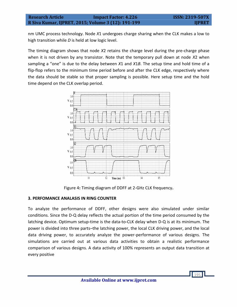
data to be sampled even after the rising edge of the CLK before CLKB falls low in fig -4 shows
the post-layout timing diagram of the flip-flop at 2-GHz CLK frequency and 1.2 V supply in 90-
Research Article Impact Factor: 4.226 ISSN: 2319-507X R Siva Kumar, IJPRET, 2015; Volume 3 (12): 191-199 IJPRET
Available Online at www.ijpret.com
195
nm UMC process technology. Node X1 undergoes charge sharing when the CLK makes a low to
high transition while D is held at low logic level.
The timing diagram shows that node X2 retains the charge level during the pre-charge phase
when it is not driven by any transistor. Note that the temporary pull down at node X2 when
sampling a “one” is due to the delay between X1 and X1B. The setup time and hold time of a
flip-flop refers to the minimum time period before and after the CLK edge, respectively where
the data should be stable so that proper sampling is possible. Here setup time and the hold
time depend on the CLK overlap period.
Figure 4: Timing diagram of DDFF at 2-GHz CLK frequency.
3. PERFOMANCE ANALASIS IN RING COUNTER
To analyze the performance of DDFF, other designs were also simulated under similar
conditions. Since the D-Q delay reflects the actual portion of the time period consumed by the
latching device. Optimum setup-time is the data-to-CLK delay when D-Q is at its minimum. The
power is divided into three parts–the latching power, the local CLK driving power, and the local
data driving power, to accurately analyze the power-performance of various designs. The
simulations are carried out at various data activities to obtain a realistic performance
comparison of various designs. A data activity of 100% represents an output data transition at
every positive

Research Article Impact Factor: 4.226 ISSN: 2319-507X R Siva Kumar, IJPRET, 2015; Volume 3 (12): 191-199 IJPRET
Available Online at www.ijpret.com
196
CLK edge and 0% represents no data transition. Since the performance of the proposed flip-
flops depends on the CLK overlap period, a detailed analysis at various process and
temperature corners is carried out.
Figure 5: 4-bit Ring Counter
Since static leakage power is one of the major sources of power dissipation at scaled down
technology nodes, comparison of the leakage performance of various designs has been carried
out. The leakage currents for different input and output conditions are measured to find the
reason for leakage power. In addition, all the designs were analyzed at different voltage points
to understand the impact of supply voltage fluctuation in the functionality of the flip-flops.
Finally, a 4-b ring counter is designed to highlight the performance of the proposed flip-flop
architecture. The reason for considering a ring counter is that the data activity at each bit
position is known. The most significant bit (MSB) has the least data activity (12.5%), whereas
the least significant bit (LSB) has the maximum (100%).
4. OBSERVATIONS
The performance of the proposed DD-FF design is evaluated against existing designs through
post-layout simulations. The compared designs include four explicit type P-FF designs shown in
Fig. 2, an Pulse triggered flip flop design shown in fig. 1 A conventional CMOS NAND-logic-
based pulse generator design with a three-stage inverter chain is used for DDFF designs, which
employs its own pulse generation circuitry.
Type of FF Power Delay (ns) Power Delay Product
Existing D-FF 8.37 0.57 4.77 Explicit P-FF 6.34 0.23 1.45 DD FF 6.14 0.18 1.10 Ring Counter 3.92 0.55 2.15
Table -1: Performance Analysis Table for various types of FFs

Research Article Impact Factor: 4.226 ISSN: 2319-507X R Siva Kumar, IJPRET, 2015; Volume 3 (12): 191-199 IJPRET
Available Online at www.ijpret.com
197
Chart-1: Performance Analysis Chart for various type of FFs
4. CONCLUSION
In this paper, a new low power DDFF was proposed. An analysis of the overlap period required
to select proper pulse width was provided in order to make the design process simpler. The
proposed DDFF eliminates the redundant power dissipation present in the pulse triggered FF. A
comparison of the proposed DD flip-flop with the conventional flip-flops showed that it exhibits
lower power dissipation along with comparable speed performances. The post-layout
simulation results showed an improvement in PDP by about 10% compared to the P-FF at 25%
data activity. By eliminating the charge sharing problem, the revised structure of the proposed
flip-flop, The efficiency of the flip-flop is highlighted using a 4-b ring counter. It was proven that
the proposed architectures are well suited for modern high performance designs where area,
delay-overhead, and power dissipation are of major concern
ACKNOWLEDGEMENT
I would like to express my gratitude to the following people for their support and guidance for
the success of this paper.
First & foremost we would like to thank our mentor & guide Mrs. T Srinivasa Padmaja Associate
Professor of ECE, SIETK, Puttur, for his constant support & guidance. His active cooperation &
involvement have helped us through the various stages of project development.

Research Article Impact Factor: 4.226 ISSN: 2319-507X R Siva Kumar, IJPRET, 2015; Volume 3 (12): 191-199 IJPRET
Available Online at www.ijpret.com
198
REFERENCES
1. “Low-Power Pulse-Triggered Flip-Flop Design Based on a Signal Feed-Through Scheme”, Jin-
Fa Lin, IEEE TRANSACTIONS ON VERY LARGE SCALE INTEGRATION (VLSI) SYSTEMS, VOL. 22, NO.
1, JANUARY 2014
2. H. Kawaguchi and T. Sakurai, “A reduced clock-swing flip-flop (RCSFF) for 63% power
reduction”, IEEE J. Solid-State Circuits, vol. 33, no. 5, pp. 807–811, May 1998.
3. K. Chen, “A 77% energy saving 22-transistor single phase clocking D-flip-flop with adoptive-
coupling configuration in 40 nm CMOS”, in Proc. IEEE Int. Solid-State Circuits Conf., Nov. 2011,
pp. 338–339.
4. E. Consoli, M. Alioto, G. Palumbo, and J. Rabaey, “Conditional push pull pulsed latch with 726
fJops energy delay product in 65 nm MOS”, in Proc. IEEE Int. Solid-State Circuits Conf., Feb.
2012, pp. 482–483.
5. H. Partovi, R. Burd, U. Salim, F.Weber, L. DiGregorio, and D. Draper, “Flow-through latch and
edge-triggered flip-flop hybrid elements”, in Proc. IEEE Int. Solid-State Circuits Conf., Feb. 1996,
pp. 138–139.
6. F. Klass, C. Amir, A. Das, K. Aingaran, C. Truong, R. Wang, A. Mehta, R. Heald, and G. Yee, “A
new family of semi-dynamic and dynamic flip-flops with embedded logic for high-performance
processors”, IEEE J. Solid-State Circuits, vol. 34, no. 5, pp. 712–716, May 1999
7. Low-Power Dual Dynamic Node Pulsed Hybrid Flip-Flop Featuring Efficient Embedded Logic”,
Kalarikkal Absel, Lijo Manuel, and R. K. Kavitha, Member, IEEE, IEEE TRANSACTIONS ON VERY
LARGE SCALE INTEGRATION (VLSI) SYSTEMS, VOL. 21, NO. 9, SEPTEMBER 2013.
8. B.-S. Kong, S.-S. Kim, and Y.-H. Jun, “Conditional-capture flip-flop for statistical power
reduction”, IEEE J. Solid-State Circuits, vol. 36, no. 8, pp. 1263–1271, Aug. 2001.
9. Stojanovic and V. Oklobdzija, “Comparative analysis of masterslave latches and flip-flops for
high-performance and low-power systems”, IEEE J. Solid-State Circuits, vol. 34, no. 4, pp. 536–
548, Apr. 1999.
10. Nedovic, M. Aleksic, and V. G. Oklobdzija, “Conditional pre-charge techniques for power-
efficient dual-edge clocking”, in Proc. Int. Symp. Low-Power Electron. Design, 2002, pp. 56–59.

Research Article Impact Factor: 4.226 ISSN: 2319-507X R Siva Kumar, IJPRET, 2015; Volume 3 (12): 191-199 IJPRET
Available Online at www.ijpret.com
199
11. C. K. Teh, M. Hamada, T. Fujita, H. Hara, N. Ikumi, and Y. Oowaki, “Conditional data
applying flip-flops for low-power and high performance systems”, IEEE Trans. Very Large
Scale Integer. (VLSI) Syst., vol. 14, no. 12, pp. 1379–1383, Dec. 2006.
12. S. H. Rasouli, A. Khademzadeh, A. Afzali-Kusha, and M. Nourani, “Low-power single- and
double-edge-triggered flip-flops for high-speed applications”, Proc. Inst. Elect. Eng. Circuits
Devices Syst., vol. 152, no. 2, pp. 118–122, Apr. 2005