
Interleaved High-Efficiency, Dual Power-Supply Controllers ... · PDF fileCSL1 CSH1 BST1 DH1...
30
General Description The MAX8716/MAX8717/MAX8756/MAX8757 are dual, step-down, interleaved, fixed-frequency, switch-mode power-supply (SMPS) controllers with synchronous rec- tification. The MAX8716/MAX8717/MAX8756/MAX8757 are intended for main (5V/3.3V) power generation, while the MAX8756 is optimized for I/O power rails in battery- powered systems. Fixed-frequency operation with optimal interleaving min- imizes input ripple current from the lowest input voltages up to the 26V maximum input. Optimal 40/60 interleav- ing allows the input voltage to go down to 8.3V before duty-cycle overlap occurs in 5V/3.3V applications, com- pared to 180° out-of-phase regulators where the duty- cycle overlap occurs when the input drops below 10V. Accurate output current limit is achieved using a sense resistor. Alternatively, power dissipation can be reduced using lossless inductor current sensing. Independent ON/OFF controls and power-good signals allow flexible power sequencing. Soft-start reduces inrush current, while soft-stop gradually ramps the out- put voltage down preventing negative voltage dips. A low-noise mode maintains high light-load efficiency while keeping the switching frequency out of the audi- ble range. The MAX8716 is available in a 24-pin thin QFN pack- age, and the MAX8717/MAX8756/MAX8757 are avail- able in a 28-pin thin QFN package. Applications 2 to 4 Li+ Cell Battery-Powered Devices Notebook and Subnotebook Computers PDAs and Mobile Communicators Main or I/O Power Supplies Features ♦ Fixed Switching Frequency 200kHz, 300kHz, or 500kHz 250kHz, 300kHz, or 400kHz (MAX8756 Only) ♦ No Current-Sense Resistor Required ♦ 40/60 Optimal Interleaving ♦ Reduced Input-Capacitor Requirement ♦ Output Voltage Fixed or Adjustable Outputs (Dual Mode™) 3.3V/5V Fixed or 1V to 5.5V Adjustable 1.5V/1.8V Fixed or 1V to 2.3V Adjustable (MAX8756 Only) ♦ 4V to 26V Input Range ♦ Independently Selectable PWM, Skip, and Low- Noise Mode Operation ♦ Soft-Start and Soft-Stop ♦ 2V Precision Reference with 0.75% Accuracy ♦ Independent Power-Good Outputs MAX8716/MAX8717/MAX8756/MAX8757 Interleaved High-Efficiency, Dual Power-Supply Controllers for Notebook Computers ________________________________________________________________ Maxim Integrated Products 1 24 23 22 21 20 19 PGOOD1 A "+" SIGN WILL REPLACE THE FIRST PIN INDICATOR ON LEAD-FREE PACKAGES. FB1 CSL1 CSH1 BST1 DH1 7 8 9 10 11 12 PGOOD2 FB2 CSL2 CSH2 BST2 DH2 13 14 15 16 17 18 LX2 DL2 V DD GND DL1 LX1 6 5 4 3 2 1 ON2 ON1 SKIP2 REF SKIP1 V CC MAX8716ETG TOP VIEW 28 27 26 25 24 23 22 8 9 10 11 12 13 14 15 16 17 18 19 20 21 7 6 5 4 3 2 1 MAX8717ETI MAX8756ETI+ MAX8757ETI+ TQFN TQFN TOP VIEW SKIP1 V CC REF SKIP2 FSEL ON1 ON2 ILIM1 PGOOD1 FB1 CSL1 CSH1 BST1 DH1 LX1 DL1 AGND PGND V DD DL2 LX2 DH2 BST2 CSH2 CSL2 FB2 PGOOD2 ILIM2 + + Pin Configurations Ordering Information 19-3569; Rev 2; 4/07 For pricing, delivery, and ordering information, please contact Maxim/Dallas Direct! at 1-888-629-4642, or visit Maxim’s website at www.maxim-ic.com. PART TEMP RANGE PIN- PACKAGE PKG CODE MAX8716ETG -40°C to +85°C 24 Thin QFN 4mm x 4mm T2444-4 MAX8716ETG+ -40°C to +85°C 24 Thin QFN 4mm x 4mm T2444-4 MAX8717ETI -40°C to +85°C 28 Thin QFN 5mm x 5mm T2855-6 Dual Mode is a trademark of Maxim Integrated Products, Inc. +Denotes a lead-free package. Ordering Information continued at end of data sheet. EVALUATION KIT AVAILABLE
Transcript of Interleaved High-Efficiency, Dual Power-Supply Controllers ... · PDF fileCSL1 CSH1 BST1 DH1...

General DescriptionThe MAX8716/MAX8717/MAX8756/MAX8757 are dual,step-down, interleaved, fixed-frequency, switch-modepower-supply (SMPS) controllers with synchronous rec-tification. The MAX8716/MAX8717/MAX8756/MAX8757are intended for main (5V/3.3V) power generation, whilethe MAX8756 is optimized for I/O power rails in battery-powered systems.Fixed-frequency operation with optimal interleaving min-imizes input ripple current from the lowest input voltagesup to the 26V maximum input. Optimal 40/60 interleav-ing allows the input voltage to go down to 8.3V beforeduty-cycle overlap occurs in 5V/3.3V applications, com-pared to 180° out-of-phase regulators where the duty-cycle overlap occurs when the input drops below 10V.Accurate output current limit is achieved using a senseresistor. Alternatively, power dissipation can bereduced using lossless inductor current sensing.Independent ON/OFF controls and power-good signalsallow flexible power sequencing. Soft-start reducesinrush current, while soft-stop gradually ramps the out-put voltage down preventing negative voltage dips. A low-noise mode maintains high light-load efficiencywhile keeping the switching frequency out of the audi-ble range.The MAX8716 is available in a 24-pin thin QFN pack-age, and the MAX8717/MAX8756/MAX8757 are avail-able in a 28-pin thin QFN package.
Applications2 to 4 Li+ Cell Battery-Powered DevicesNotebook and Subnotebook ComputersPDAs and Mobile CommunicatorsMain or I/O Power Supplies
Features� Fixed Switching Frequency
200kHz, 300kHz, or 500kHz250kHz, 300kHz, or 400kHz (MAX8756 Only)
� No Current-Sense Resistor Required� 40/60 Optimal Interleaving� Reduced Input-Capacitor Requirement� Output Voltage Fixed or Adjustable Outputs
(Dual Mode™)3.3V/5V Fixed or 1V to 5.5V Adjustable1.5V/1.8V Fixed or 1V to 2.3V Adjustable (MAX8756 Only)
� 4V to 26V Input Range� Independently Selectable PWM, Skip, and Low-
Noise Mode Operation� Soft-Start and Soft-Stop� 2V Precision Reference with 0.75% Accuracy� Independent Power-Good Outputs
MA
X8
71
6/M
AX
87
17
/MA
X8
75
6/M
AX
87
57
Interleaved High-Efficiency, Dual Power-SupplyControllers for Notebook Computers
________________________________________________________________ Maxim Integrated Products 1
24
23
22
21
20
19
PGOOD1
A "+" SIGN WILL REPLACE THE FIRST PIN INDICATOR ON LEAD-FREE PACKAGES.
FB1
CSL1
CSH1
BST1
DH1
7
8
9
10
11
12
PGOOD2
FB2
CSL2
CSH2
BST2
DH2
131415161718
LX2
DL2
V DD
GND
DL1
LX1
654321
ON2
ON1
SKIP
2
REF
SKIP
1
V CC
MAX8716ETG
TOP VIEW
28
27
26
25
24
23
22
8
9
10
11
12
13
14
15161718192021
7654321
MAX8717ETIMAX8756ETI+MAX8757ETI+
TQFN
TQFN
TOP VIEW
SKIP
1
V CC
REF
SKIP
2
FSEL
ON1
ON2
ILIM1
PGOOD1
FB1
CSL1
CSH1
BST1
DH1
LX1
DL1
AGND
PGND
V DD
DL2
LX2
DH2
BST2
CSH2
CSL2
FB2
PGOOD2
ILIM2+
+
Pin Configurations
Ordering Information
19-3569; Rev 2; 4/07
For pricing, delivery, and ordering information, please contact Maxim/Dallas Direct! at 1-888-629-4642, or visit Maxim’s website at www.maxim-ic.com.
PART TEMP RANGEPIN-PACKAGE
PKGCODE
MAX8716ETG -40°C to +85°C24 Thin QFN4mm x 4mm
T2444-4
MAX8716ETG+ -40°C to +85°C24 Thin QFN4mm x 4mm
T2444-4
MAX8717ETI -40°C to +85°C28 Thin QFN5mm x 5mm
T2855-6
Dual Mode is a trademark of Maxim Integrated Products, Inc.
+Denotes a lead-free package.
Ordering Information continued at end of data sheet.
EVALUATION KIT
AVAILABLE

MA
X8
71
6/M
AX
87
17
/MA
X8
75
6/M
AX
87
57
Interleaved High-Efficiency, Dual Power-SupplyControllers for Notebook Computers
2 _______________________________________________________________________________________
ABSOLUTE MAXIMUM RATINGS (Note 1)
Stresses beyond those listed under “Absolute Maximum Ratings” may cause permanent damage to the device. These are stress ratings only, and functionaloperation of the device at these or any other conditions beyond those indicated in the operational sections of the specifications is not implied. Exposure toabsolute maximum rating conditions for extended periods may affect device reliability.
VDD, VCC, CSL1, CSH1, CSL2, CSH2 to AGND ......-0.3V to +6VON1, ON2, SKIP1, SKIP2, PGOOD1,
PGOOD2 to AGND...............................................-0.3V to +6VFB1, FB2, ILIM1, ILIM2, FSEL to AGND...................-0.3V to +6VREF to AGND..............................................-0.3V to (VCC + 0.3V)BST1, BST2 to AGND.............................................-0.3V to +36VLX1 to BST1..............................................................-6V to +0.3VLX2 to BST2..............................................................-6V to +0.3V DH1 to LX1 ..............................................-0.3V to (VBST1 + 0.3V)DH2 to LX2 ..............................................-0.3V to (VBST2 + 0.3V)DL1, DL2 to PGND .....................................-0.3V to (VDD + 0.3V)AGND to PGND.....................................................-0.3V to +0.3V
REF Short Circuit to AGND.........................................ContinuousREF Current ......................................................................+10mAContinuous Power Dissipation (TA = +70°C)
24-Pin Thin QFN 4mm x 4mm (derate 20.8mW/°C above +70°C)..........................................................1666.7mW28-Pin Thin QFN 5mm x 5mm (derate 21.3mW/°Cabove +70°C)..........................................................1702.1mW
Operating Temperature Range ...........................-40°C to +85°CJunction Temperature ......................................................+150°CStorage Temperature Range .............................-65°C to +150°CLead Temperature (soldering, 10s) .................................+300°C
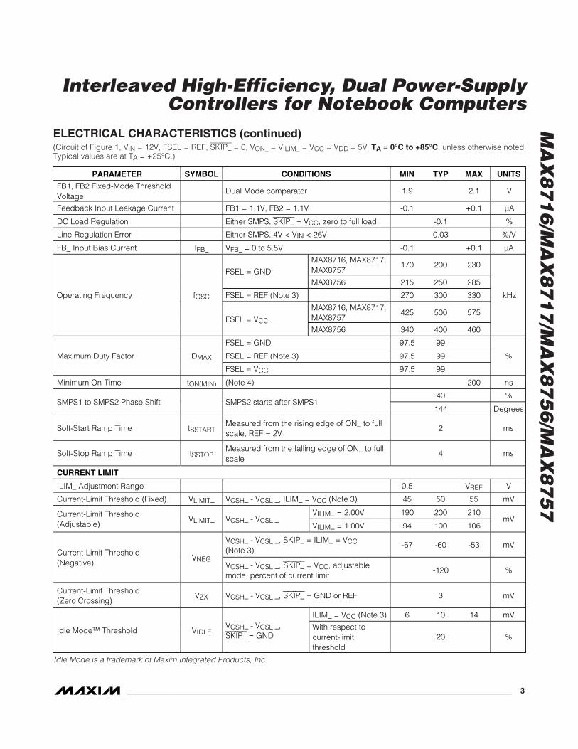
ELECTRICAL CHARACTERISTICS(Circuit of Figure 1, VIN = 12V, FSEL = REF, SKIP_ = 0, VON_ = VILIM_ = VCC = VDD = 5V, TA = 0°C to +85°C, unless otherwise noted.Typical values are at TA = +25°C.)
PARAMETER SYMBOL CONDITIONS MIN TYP MAX UNITS
INPUT SUPPLIES
VIN 26Input Voltage Range
VBIAS VCC, VDD 4.5 5.5V
VCC rising 3.9 4.15 4.4VCC Undervoltage-LockoutThreshold
VUVLO200mV typicalhysteresis VCC falling 3.7 3.95 4.2
V
MAX8716, MAX8717,MAX8757
0.8 1.3Quiescent Supply Current (VCC) ICC
CSL_ and FB_ forcedabove their regulationpoints MAX8756 1 1.8
mA
Quiescent Supply Current (VDD) IDDCSL_ and FB_ forced above their regulationpoints
< 1 5 µA
Shutdown Supply Current (VCC) ON1 = ON2 = GND < 1 5 µA
Shutdown Supply Current (VDD) ON1 = ON2 = GND < 1 5 µA
MAIN SMPS CONTROLLERS
MAX8716, MAX8717,MAX8757
3.265 3.30 3.365PWM1 Output Voltage inFixed Mode
VOUT1
VIN = 6V to 26V,SKIP1 = VCC,zero to full load MAX8756 1.484 1.50 1.530
V
MAX8716, MAX8717,MAX8757
4.94 5.00 5.09PWM2 Output Voltage inFixed Mode
VOUT2
VIN = 6V to 26V,SKIP2 = VCC,zero to full load MAX8756 1.778 1.800 1.832
V
VIN = 6V to 26V, FB1 or FB2,duty factor = 20% to 80%
0.990 1.005 1.020Feedback Voltage in AdjustableMode (Note 2)
VFB_ VIN = 6V to 26V, FB1 or FB2,duty factor = 50%
0.995 1.005 1.015V
MAX8716, MAX8717,MAX8757
1.0 5.5Output-Voltage-Adjust Range Either SMPS
MAX8756 1.0 2.3V
Note 1: For the 24-pin TQFN version, AGND and PGND refer to a single pin designated GND.
MA
X8
71
6/M
AX
87
17
/MA
X8
75
6/M
AX
87
57
Interleaved High-Efficiency, Dual Power-SupplyControllers for Notebook Computers
_______________________________________________________________________________________ 3
ELECTRICAL CHARACTERISTICS (continued)(Circuit of Figure 1, VIN = 12V, FSEL = REF, SKIP_ = 0, VON_ = VILIM_ = VCC = VDD = 5V, TA = 0°C to +85°C, unless otherwise noted.Typical values are at TA = +25°C.)
PARAMETER SYMBOL CONDITIONS MIN TYP MAX UNITS
FB1, FB2 Fixed-Mode ThresholdVoltage
Dual Mode comparator 1.9 2.1 V
Feedback Input Leakage Current FB1 = 1.1V, FB2 = 1.1V -0.1 +0.1 µA
DC Load Regulation Either SMPS, SKIP_ = VCC, zero to full load -0.1 %
Line-Regulation Error Either SMPS, 4V < VIN < 26V 0.03 %/V
FB_ Input Bias Current IFB_ VFB_ = 0 to 5.5V -0.1 +0.1 µA
MAX8716, MAX8717,MAX8757
170 200 230FSEL = GND
MAX8756 215 250 285
FSEL = REF (Note 3) 270 300 330
MAX8716, MAX8717,MAX8757
425 500 575
Operating Frequency fOSC
FSEL = VCCMAX8756 340 400 460
kHz
FSEL = GND 97.5 99
FSEL = REF (Note 3) 97.5 99Maximum Duty Factor DMAX
FSEL = VCC 97.5 99
%
Minimum On-Time tON(MIN) (Note 4) 200 ns
40 %SMPS1 to SMPS2 Phase Shift SMPS2 starts after SMPS1
144 Degrees
Soft-Start Ramp Time tSSTARTMeasured from the rising edge of ON_ to fullscale, REF = 2V
2 ms
Soft-Stop Ramp Time tSSTOPMeasured from the falling edge of ON_ to fullscale
4 ms
CURRENT LIMIT
ILIM_ Adjustment Range 0.5 VREF V
Current-Limit Threshold (Fixed) VLIMIT_ VCSH_ - VCSL _, ILIM_ = VCC (Note 3) 45 50 55 mV
VILIM_ = 2.00V 190 200 210Current-Limit Threshold(Adjustable)
VLIMIT_ VCSH_ - VCSL _VILIM_ = 1.00V 94 100 106
mV
VCSH_ - VCSL _, SKIP_ = ILIM_ = VCC(Note 3)
-67 -60 -53 mVCurrent-Limit Threshold(Negative)
VNEGVCSH_ - VCSL _, SKIP_ = VCC, adjustablemode, percent of current limit
-120 %
Current-Limit Threshold(Zero Crossing)
VZX VCSH_ - VCSL _, SKIP_ = GND or REF 3 mV
ILIM_ = VCC (Note 3) 6 10 14 mV
Idle Mode™ Threshold VIDLEVCSH_ - VCSL _,SKIP_ = GND
With respect tocurrent-limitthreshold
20 %
Idle Mode is a trademark of Maxim Integrated Products, Inc.

MA
X8
71
6/M
AX
87
17
/MA
X8
75
6/M
AX
87
57
Interleaved High-Efficiency, Dual Power-SupplyControllers for Notebook Computers
4 _______________________________________________________________________________________
ELECTRICAL CHARACTERISTICS (continued)(Circuit of Figure 1, VIN = 12V, FSEL = REF, SKIP_ = 0, VON_ = VILIM_ = VCC = VDD = 5V, TA = 0°C to +85°C, unless otherwise noted.Typical values are at TA = +25°C.)
PARAMETER SYMBOL CONDITIONS MIN TYP MAX UNITS
M AX 8716, M AX 8717,M AX 8757
2.5 5 7.5VCSH_ - VCSL_SKIP_ = REFILIM_ = VCC (Note 3) MAX8756 1 2.5 4
mV
M AX 8716, M AX 8717,M AX 8757
10Low-Noise-Mode Threshold VIDLE VCSH_ - VCSL_
SKIP_ = REF withrespect to current-limit threshold
MAX8756 5%
ILIM_ Leakage Current 0.1 µA
Reference Load Regulation ΔVREF IREF = 0µA to 50µA 10 mV
Reference Sink Current 10 µA
REF Lockout Voltage VREF(UVLO) Rising edge, hysteresis = 50mV 1.8 V
FAULT DETECTION
Output Overvoltage TripThreshold
MAX8716/MAX8717/MAX8756 only 11 15 19 %
Output OvervoltageFault-Propagation Delay
tOVP50mV overdrive,MAX8716/MAX8717/MAX8756 only
10 µs
Output Undervoltage-ProtectionTrip Threshold
With respect to error-comparator threshold 65 70 75 %
Output UndervoltageFault-Propagation Delay
tUVP 50mV overdrive 10 µs
Output Undervoltage-ProtectionBlanking Time
tBLANK From rising edge of ON_ 6144 1/fOSC
PGOOD_ Lower Trip ThresholdWith respect to error-comparator threshold,hysteresis = 1%
-12.5 -10 -8.0 %
PGOOD_ Propagation Delay tPGOOD_ Falling edge, 50mV overdrive 10 µs
PGOOD_ Output Low Voltage ISINK = 4mA 0.4 V
PGOOD_ Leakage Current IPGOOD_ High state, PGOOD_ forced to 5.5V 1 µA
Thermal-Shutdown Threshold TSHDN Hysteresis = 15°C +160 °C
GATE DRIVERS
DH_ Gate-Driver On-Resistance RDH BST_ - LX_ forced to 5V (Note 5) 1.5 5 Ω
DL_, high state 1.7 5DL_ Gate-Driver On-Resistance(Note 5)
RDLDL_, low state 0.6 3
Ω
DH_ Gate-Driver Source/SinkCurrent
IDHDH_ forced to 2.5V, BST_ - LX_ forced to5V
2 A
DL_ Gate-Driver Source CurrentIDL
(SOURCE)DL_ forced to 2.5V 1.7 A
DL_ Gate-Driver Sink Current IDL (SINK) DL_ forced to 2.5V 3.3 A
DL_ rising 35Dead Time tDEAD
DH_ rising 26ns
LX_, BST_ Leakage Current VBST_ = VLX_ = 26V < 2 20 µA

MA
X8
71
6/M
AX
87
17
/MA
X8
75
6/M
AX
87
57
Interleaved High-Efficiency, Dual Power-SupplyControllers for Notebook Computers
_______________________________________________________________________________________ 5
PARAMETER SYMBOL CONDITIONS MIN TYP MAX UNITS
INPUTS AND OUTPUTS
Logic Input Current ON1, ON2 -1 +1 µA
ON_ Input Voltage Rising edge, hysteresis = 225mV 1.2 1.7 2.2 V
Tri-Level Input Logic SKIP1, SKIP2, FSEL, highVCC -0.2
V
Input Leakage Current SKIP1, SKIP2, FSEL, 0V, or VCC -3 +3 µA
Input Leakage Current ILIM1, ILIM2, 0V, or VCC -0.1 +0.1 µA
Input Leakage Current CSH_, 0V, or VDD -0.1 +0.1 µA
Input Bias Current CSL_, 0V, or VDD 25 50 µA
ELECTRICAL CHARACTERISTICS (continued)(Circuit of Figure 1, VIN = 12V, FSEL = REF, SKIP_ = 0, VON_ = VILIM_ = VCC = VDD = 5V, TA = 0°C to +85°C, unless otherwise noted.Typical values are at TA = +25°C.)
ELECTRICAL CHARACTERISTICS(Circuit of Figure 1, VIN = 12V, FSEL = REF, SKIP_ = 0, VON_ = VILIM_ = VCC = VDD = 5V, TA = -40°C to +85°C, unless otherwisenoted.) (Note 6)
PARAMETER SYMBOL CONDITIONS MIN TYP MAX UNITS
INPUT SUPPLIES
VIN 26Input Voltage Range
VBIAS VCC, VDD 4.5 5.5V
MAX8716, MAX8717,MAX8757
1.3Quiescent Supply Current (VCC) ICC
CSL_ and FB_forced above theirregulation points MAX8756 1.8
mA
Quiescent Supply Current (VDD) IDDCSL_ and FB_ forced above their regulationpoints
5 µA
Shutdown Supply Current (VCC) ON1 = ON2 = GND 5 µA
Shutdown Supply Current (VDD) ON1 = ON2 = GND 5 µA
MAIN SMPS CONTROLLERSMAX8716, MAX8717,MAX8757
3.255 3.375PWM1 Output Voltage inFixed Mode
VOUT1
VIN = 6V to 26V,SKIP1 = VCC,zero to full load MAX8756 1.480 1.534
V
MAX8716, MAX8717,MAX8757
4.925 5.105PWM2 Output Voltage inFixed Mode
VOUT2
VIN = 6V to 26V,SKIP2 = VCC,zero to full load MAX8756 1.773 1.838
V
Feedback Voltage inAdjustable Mode
VFB_VIN = 6V to 26V, FB1 or FB2,duty factor = 20% to 80% (Note 1)
0.987 1.023 V
MAX8716, MAX8717,MAX8757
1.0 5.5Output Voltage Adjust Range Either SMPS
MAX8756 1.0 2.3V
FB1, FB2 Fixed-ModeThreshold Voltage
Dual Mode comparator 1.9 2.1 V

MA
X8
71
6/M
AX
87
17
/MA
X8
75
6/M
AX
87
57
Interleaved High-Efficiency, Dual Power-SupplyControllers for Notebook Computers
6 _______________________________________________________________________________________
ELECTRICAL CHARACTERISTICS (continued)(Circuit of Figure 1, VIN = 12V, FSEL = REF, SKIP_ = 0, VON_ = VILIM_ = VCC = VDD = 5V, TA = -40°C to +85°C, unless otherwisenoted.) (Note 6)
PARAMETER SYMBOL CONDITIONS MIN TYP MAX UNITS
MAX8716, MAX8717,MAX8757
170 230FSEL = GND
MAX8756 215 285
FSEL = REF (Note 3) 270 330
MAX8716, MAX8717,MAX8757
425 575
Operating Frequency fOSC
FSEL = VCCMAX8756 340 460
kHz
FSEL = GND 97.5
FSEL = REF (Note 3) 97.5Maximum Duty Factor DMAX
FSEL = VCC 97.5
%
Minimum On-Time tON(MIN) (Note 4) 200 ns
CURRENT LIMIT
ILIM_ Adjustment Range 0.5 VREF V
Current-Limit Threshold (Fixed) VLIMIT_ VCSH_ - VCSL _, ILIM_ = VCC (Note 3) 44 56 mV
VILIM_ = 2.00V 188 212Current-Limit Threshold(Adjustable)
VLIMIT_ VCSH_ - VCSL _VILIM_ = 1.00V 93 107
mV
REFERENCE (REF)
Reference Voltage VREF VCC = 4.5V to 5.5V, IREF = 0 1.98 2.02 V
FAULT DETECTION
O utp ut O ver vol tag e Tr i p Thr eshol d MAX8716/MAX8717/MAX8756 only 11 19 %
Output Undervoltage-ProtectionTrip Threshold
With respect to error-comparator threshold 65 75 %
PGOOD_ Lower Trip ThresholdWith respect to error-comparator threshold,hysteresis = 1%
-12.5 -8.0 %
PGOOD_ Output Low Voltage ISINK = 4mA 0.4 V
GATE DRIVERS
DH_ Gate-Driver On-Resistance RDH BST_ - LX_ forced to 5V (Note 5) 5 ΩDL_, high state 5DL_ Gate-Driver On-Resistance
(Note 5)RDL
DL_, low state 3Ω
INPUTS AND OUTPUTS
ON_ Input Voltage Rising edge, hysteresis = 225mV 1.2 2.2 V
HighVCC -0.2
REF 1.7 2.3Tri-Level Input Logic SKIP1, SKIP2, FSEL
GND 0.5
V
Note 2: When the inductor is in continuous conduction, the output voltage will have a DC regulation level lower than the error-com-parator threshold by 50% of the ripple. In discontinuous conduction, the output voltage will have a DC regulation level higherthan the error-comparator threshold by 50% of the ripple.
Note 3: Default setting for the MAX8716.Note 4: Specifications are guaranteed by design, not production tested.Note 5: Production testing limitations due to package handling require relaxed maximum on-resistance specifications for the thin QFN
package.Note 6: Specifications from 0°C to -40°C are guaranteed by design, not production tested.

MA
X8
71
6/M
AX
87
17
/MA
X8
75
6/M
AX
87
57
Interleaved High-Efficiency, Dual Power-SupplyControllers for Notebook Computers
_______________________________________________________________________________________ 7
100
500.001 0.01 0.1 1 10
3.3V OUTPUT EFFICIENCYvs. LOAD CURRENT
60
MAX
8716
/17/
57 to
c01
LOAD CURRENT (A)
EFFI
CIEN
CY (%
)
70
80
90
VIN = 6V
SKIPMODE
LOW-NOISEMODE
PWMMODE
100
500.001 0.01 0.1 1 10
3.3V OUTPUT EFFICIENCYvs. LOAD CURRENT
60
MAX
8716
/17/
57 to
c02
LOAD CURRENT (A)
EFFI
CIEN
CY (%
)
70
80
90
VIN = 12V
SKIPMODE
PWMMODELOW-
NOISEMODE
100
500.001 0.01 0.1 1 10
3.3V OUTPUT EFFICIENCYvs. LOAD CURRENT
60
MAX
8716
/17/
57 to
c03
LOAD CURRENT (A)
EFFI
CIEN
CY (%
)
70
80
90
VIN = 20V
SKIPMODE
PWMMODELOW-
NOISEMODE
3.3V OUTPUT VOLTAGEvs. LOAD CURRENT
MAX
8716
/17/
57 to
c04
LOAD CURRENT (A)
OUTP
UT V
OLTA
GE (V
)
4321
3.30
3.35
3.40
3.250 5
SKIPMODE
PWMMODE
VIN = 12V
LOW-NOISEMODE
100
500.001 0.01 0.1 1 10
5V OUTPUT EFFICIENCYvs. LOAD CURRENT
60
MAX
8716
/17/
57 to
c05
LOAD CURRENT (A)
EFFI
CIEN
CY (%
)
70
80
90
PWMMODE
VIN = 6V
LOW-NOISEMODE
SKIPMODE
100
500.001 0.01 0.1 1 10
5V OUTPUT EFFICIENCYvs. LOAD CURRENT
60
MAX
8716
/17/
57 to
c06
LOAD CURRENT (A)
EFFI
CIEN
CY (%
)
70
80
90
VIN = 12V
SKIPMODE
PWMMODE
LOW-NOISEMODE
100
500.001 0.01 0.1 1 10
5V OUTPUT EFFICIENCYvs. LOAD CURRENT
60
MAX
8716
/17/
57 to
c07
LOAD CURRENT (A)
EFFI
CIEN
CY (%
)
70
80
90
VIN = 20V
SKIPMODE
PWMMODE
LOW-NOISEMODE
5V OUTPUT VOLTAGEvs. LOAD CURRENT
MAX
8716
/17/
57 to
c08
LOAD CURRENT (A)
OUTP
UT V
OLTA
GE (V
)
41 32
5.00
5.05
5.10
5.15
4.950 5
SKIPMODE
PWMMODE
VIN = 12V
LOW-NOISEMODE
2.5V OUTPUT EFFICIENCYvs. LOAD CURRENT
MAX
8716
/17/
57 to
c09
LOAD CURRENT (A)
EFFI
CIEN
CY (%
)
10.10.01
60
70
80
90
100
500.001 10
SKIPMODE
PWMMODE
VIN = 12VL = 4.3μH
LOW-NOISEMODE
Typical Operating Characteristics(Circuit of Figure 1, MAX8717, VIN = 12V, VDD = VCC = 5V, SKIP_ = GND, FSEL = REF, TA = +25°C, unless otherwise noted.)

DROP
OUT
VOLT
AGE
(V)
0.1
0.2
0.3
0.4
0
OUT2 DROPOUT VOLTAGEvs. LOAD CURRENT
LOAD CURRENT (A)43210 5
MAX
8716
/17/
57 to
c17
VOUT2 = 4.8V
MA
X8
71
6/M
AX
87
17
/MA
X8
75
6/M
AX
87
57
Interleaved High-Efficiency, Dual Power-SupplyControllers for Notebook Computers
8 _______________________________________________________________________________________
Typical Operating Characteristics (continued)(Circuit of Figure 1, MAX8717, VIN = 12V, VDD = VCC = 5V, SKIP_ = GND, FSEL = REF, TA = +25°C, unless otherwise noted.)
1.8V OUTPUT EFFICIENCYvs. LOAD CURRENT
MAX
8716
/17/
57 to
c10
LOAD CURRENT (A)
EFFI
CIEN
CY (%
)
10.10.01
60
70
80
90
100
500.001 10
SKIPMODE
PWMMODE
VIN = 12VL = 3.2μH
LOW-NOISEMODE
NO-LOAD SUPPLY CURRENT vs. INPUTVOLTAGE (FORCED-PWM MODE)
INPUT VOLTAGE (V)
SUPP
LY C
URRE
NT (m
A)
20161284
4
8
12
16
20
24
28
00 24
MAX
8716
/17/
57 to
c11
IBIAS
IIN
SKIP1 = SKIP2 = VCCON1 = ON2 = VCC
0.1
1
10
0.01
NO-LOAD SUPPLY CURRENT vs. INPUTVOLTAGE (IDLE MODE)
INPUT VOLTAGE (V)
SUPP
LY C
URRE
NT (m
A)
201612840 24
MAX
8716
/17/
57 to
c12
IBIAS
IIN
SKIP1 = SKIP2 = GND OR REFON1 = ON2 = VCC
OUT2 IDLE-MODE CURRENT vs. INPUT VOLTAGE
IDLE
-MOD
E CU
RREN
T (A
)
0.2
0.4
0.6
0.8
1.0
1.2
1.4
1.6
1.8
2.0
0
INPUT VOLTAGE (V)201612840 24
MAX
8716
/17/
57 to
c13
MAXIMUM DUTY-CYCLE LIMITED
SKIP2 = GND
SKIP2 = REF
OUT2 SWITCHING FREQUENCYvs. LOAD CURRENT
LOAD CURRENT (A)
SWIT
CHIN
G FR
EQUE
NCY
(kHz
)
10.10.01
10
100
1000
10.001 10
MAX
8716
/17/
57 to
c14
SKIP2 = GND
SKIP2 = REF
SKIP2 = VCC
5V OUTPUT VOLTAGE vs. INPUT VOLTAGE
OUTP
UT V
OLTA
GE (V
)
4.95
5.00
5.05
4.90
INPUT VOLTAGE (V)201612840 24
MAX
8716
/17/
57 to
c15
SKIP2 = VCC
3.3V OUTPUT VOLTAGE vs. INPUT VOLTAGE
OUTP
UT V
OLTA
GE (V
)
3.30
3.35
3.40
3.25
INPUT VOLTAGE (V)201612840 24
MAX
8716
/17/
57 to
c16
SKIP1 = VCC

STARTUP WAVEFORMSMAX8716/17/57 toc18
400μs/div
0
2V
00
0
0
0
A. LX2, 20V/divB. ON2, 10V/divC. PGOOD2, 10V/div
D. REF, 2V/divE. OUT2, 2V/divF. ILX2, 2.5AV/div
1.0Ω LOAD ON OUT2
12VA
BC
DE
F
MA
X8
71
6/M
AX
87
17
/MA
X8
75
6/M
AX
87
57
Interleaved High-Efficiency, Dual Power-SupplyControllers for Notebook Computers
_______________________________________________________________________________________ 9
SHUTDOWN WAVEFORMSMAX8716/17/57 toc19
1ms/div
2V
0
0
0
A. DL2, 10V/divB. ON2, 10V/divC. PGOOD2, 10V/div
D. REF, 2V/divE. OUT2, 2V/divF. ILX2, 2.5AV/div
5V
5V5V
5V
A
BC
D
E
F
1.0kΩ LOAD ON OUT2SKIP2 = GND
STARTUP WAVEFORMSMAX8716/17/57 toc20
1ms/div
0
0
0
0
0
A. ON1/ON2, 5V/divB. PGOOD1, 10V/divC. PGOOD2, 10V/div
D. OUT2, 2V/divE. OUT1, 2V/div
3.3V
5V
A
B
C
D
E
VCC UVLO WAVEFORMSMAX8716/17/57 toc21
4ms/div
0
0
A. VCC, 2V/divB. OUT2, 2V/divC. PGOOD2, 5V/div
D. DL2, 5V/divE. ILX2, 2.5AV/div
5V
5V
5V
5V
A
B
C
D
E
100Ω LOAD ON OUT2SKIP2 = VCC
STEADY-STATE WAVEFORMSMAX8716/17/57 toc22
2μs/div
0
0
A. OUT2, 50mV/divB. LX2, 10V/divC. VIN, 50mV/div
D. OUT1, 50mV/divE. LX1, 10V/div
5V
12V
12V
3.3V
A
B
C
D
E
1.0A LOAD ON OUT1, 1.0A LOAD ON OUT2SKIP1 = VCC, SKIP2 = VCC
Typical Operating Characteristics (continued)(Circuit of Figure 1, MAX8717, VIN = 12V, VDD = VCC = 5V, SKIP_ = GND, FSEL = REF, TA = +25°C, unless otherwise noted.)
DROPOUT WAVEFORMSMAX8716/17/57 toc23
2μs/div
0
0
A. OUT2, 50mV/divB. LX2, 10V/divC. VIN, 50mV/div
D. OUT1, 50mV/divE. LX1, 10V/div
4.9V
5V
5V
5V
3.3V
A
B
C
D
E
1.0A LOAD ON OUT1, 1.0A LOAD ON OUT2SKIP1 = VCC, SKIP2 = VCC

MA
X8
71
6/M
AX
87
17
/MA
X8
75
6/M
AX
87
57
Interleaved High-Efficiency, Dual Power-SupplyControllers for Notebook Computers
10 ______________________________________________________________________________________
SKIP1 TRANSITIONMAX8716/17/57 toc27
20μs/div
0
A. SKIP1, 5V/divB. LX1, 10V/div
C. OUT1, 50mV/divD. ILX1, 2.5A/div
0
0
12V
3.3V
2.5A
A
B
C
D
30mA LOAD ON OUT1
MAX8756 NO-LOAD SUPPLY CURRENTvs. INPUT VOLTAGE (FORCED-PWM MODE)
MAX
8716
/17/
57 to
c28
INPUT VOLTAGE (V)
SUPP
LY C
URRE
NT (m
A)
204 16128
8
4
12
20
16
28
24
00 24
SKIP1 = SKIP2 = VCCON1 = ON2 = VCC
IBIAS
IIN
MAX8756 OUT2 IDLE MODE CURRENTvs. INPUT VOLTAGE
MAX
8716
/17/
57 to
c30
INPUT VOLTAGE (V)
IDLE
MOD
E CU
RREN
T (m
A)
204 16128
0.6
1.0
1.4
1.6
2.0
0.0
0.8
1.2
1.8
0.2
0.4
0 24
SKIP2 = GND
SKIP2 = REF
MAX8756 NO-LOAD SUPPLY CURRENTvs. INPUT VOLTAGE (IDLE MODE)
MAX
8716
/17/
57 to
c29
INPUT VOLTAGE (V)
SUPP
LY C
URRE
NT (m
A)
204 16128
0.01
0.1
1
10
0.0010 24
ON1 = ON2 = VCC
IBIAS
IINSKIP_ = GND
IINSKIP_ = REF
OUT1 LOAD TRANSIENTMAX8716/17/57 toc24
20μs/div
0
0
A. CONTROL, 5V/divB. OUT1, 50mV/div
C. ILX1, 3A/divD. LX1, 10V/div
0
3.3V
3A
12V
A
B
C
D
SKIP1 = VCC
SKIP1 TRANSITIONMAX8716/17/57 toc25
20μs/div
0
A. SKIP1, 5V/divB. LX1, 10V/div
C. OUT1, 50mV/divD. ILX1, 2.5A/div
0
0
12V
3.3V
2.5A
A
B
C
D
30mA LOAD ON OUT1
SKIP1 TRANSITIONMAX8716/17/57 toc26
20μs/div
0
A. SKIP1, 5V/divB. LX1, 10V/div
C. OUT1, 50mV/divD. ILX1, 2.5A/div
0
0
12V
3.3V
2.5A
A
B
C
D
30mA LOAD ON OUT1
Typical Operating Characteristics (continued)(Circuit of Figure 1, MAX8717, VIN = 12V, VDD = VCC = 5V, SKIP_ = GND, FSEL = REF, TA = +25°C, unless otherwise noted.)
MA
X8
71
6/M
AX
87
17
/MA
X8
75
6/M
AX
87
57
Interleaved High-Efficiency, Dual Power-SupplyControllers for Notebook Computers
______________________________________________________________________________________ 11
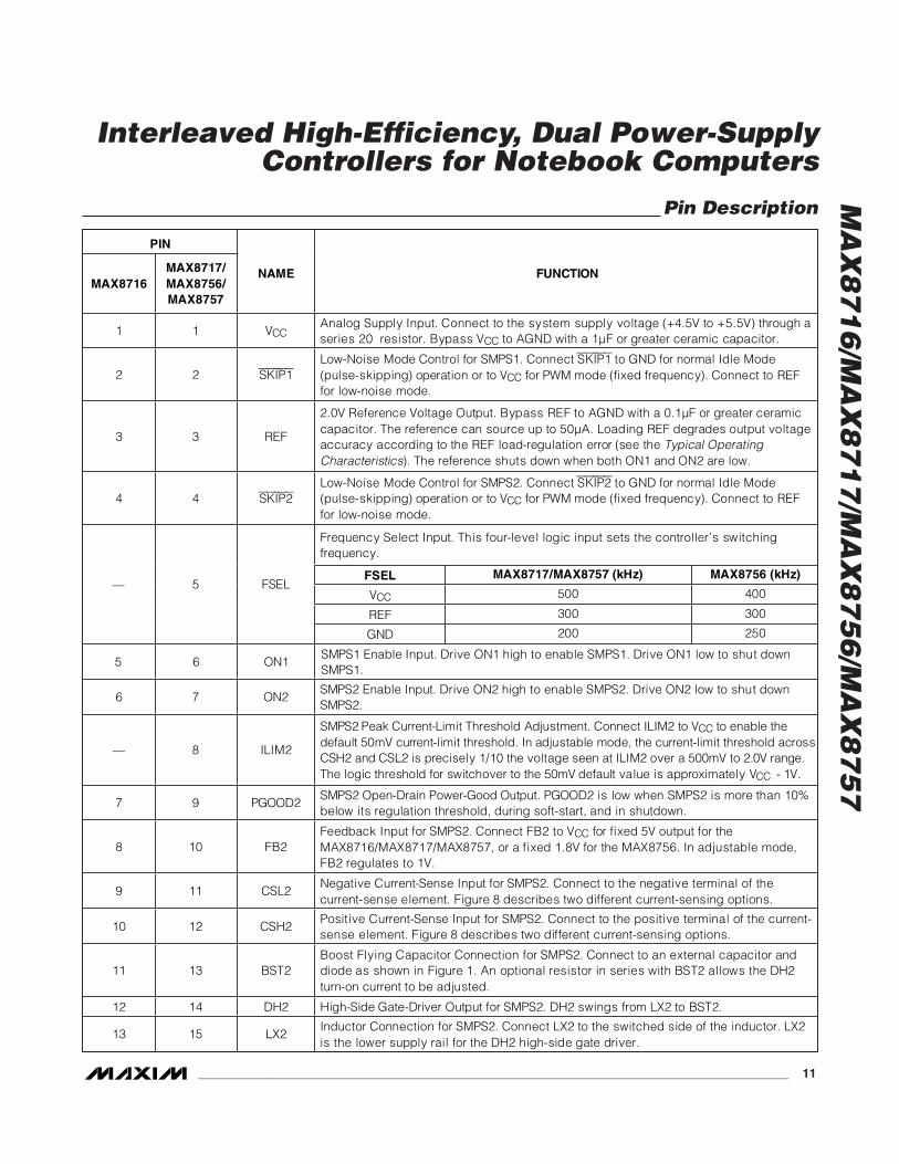
Pin Description
PIN
MAX8716MAX8717/ MAX8756/ MAX8757
NAME FUNCTION
1 1 VCC Analog Supply Input. Connect to the system supply voltage (+4.5V to +5.5V) through a series 20 resistor. Bypass VCC to AGND with a 1μF or greater ceramic capacitor.
2 2 SKIP1 Low-Noise Mode Control for SMPS1. Connect SKIP1 to GND for normal Idle Mode (pulse-skipping) operation or to VCC for PWM mode (fixed frequency). Connect to REF for low-noise mode.
3 3 REF
2.0V Reference Voltage Output. Bypass REF to AGND with a 0.1μF or greater ceramic capacitor. The reference can source up to 50μA. Loading REF degrades output voltage accuracy according to the REF load-regulation error (see the Typical Operating Characteristics). The reference shuts down when both ON1 and ON2 are low.
4 4 SKIP2 Low-Noise Mode Control for SMPS2. Connect SKIP2 to GND for normal Idle Mode (pulse-skipping) operation or to VCC for PWM mode (fixed frequency). Connect to REF for low-noise mode.
Frequency Select Input. This four-level logic input sets the controller’s switching frequency.
FSEL MAX8717/MAX8757 (kHz) MAX8756 (kHz) —
VCC 500 400
REF 300 300
5 FSEL
GND 200 250
5 6 ON1 SMPS1 Enable Input. Drive ON1 high to enable SMPS1. Drive ON1 low to shut down SMPS1.
6 7 ON2 SMPS2 Enable Input. Drive ON2 high to enable SMPS2. Drive ON2 low to shut down SMPS2.
— 8 ILIM2
SMPS2 Peak Current-Limit Threshold Adjustment. Connect ILIM2 to VCC to enable the default 50mV current-limit threshold. In adjustable mode, the current-limit threshold across CSH2 and CSL2 is precisely 1/10 the voltage seen at ILIM2 over a 500mV to 2.0V range. The logic threshold for switchover to the 50mV default value is approximately VCC - 1V.
7 9 PGOOD2 SMPS2 Open-Drain Power-Good Output. PGOOD2 is low when SMPS2 is more than 10% below its regulation threshold, during soft-start, and in shutdown.
8 10 FB2 Feedback Input for SMPS2. Connect FB2 to VCC for fixed 5V output for the MAX8716/MAX8717/MAX8757, or a fixed 1.8V for the MAX8756. In adjustable mode, FB2 regulates to 1V.
9 11 CSL2 Negative Current-Sense Input for SMPS2. Connect to the negative terminal of the current-sense element. Figure 8 describes two different current-sensing options.
10 12 CSH2 Positive Current-Sense Input for SMPS2. Connect to the positive terminal of the current-sense element. Figure 8 describes two different current-sensing options.
11 13 BST2 Boost Flying Capacitor Connection for SMPS2. Connect to an external capacitor and diode as shown in Figure 1. An optional resistor in series with BST2 allows the DH2 turn-on current to be adjusted.
12 14 DH2 High-Side Gate-Driver Output for SMPS2. DH2 swings from LX2 to BST2.
13 15 LX2 Inductor Connection for SMPS2. Connect LX2 to the switched side of the inductor. LX2 is the lower supply rail for the DH2 high-side gate driver.

MA
X8
71
6/M
AX
87
17
/MA
X8
75
6/M
AX
87
57
Interleaved High-Efficiency, Dual Power-SupplyControllers for Notebook Computers
12 ______________________________________________________________________________________
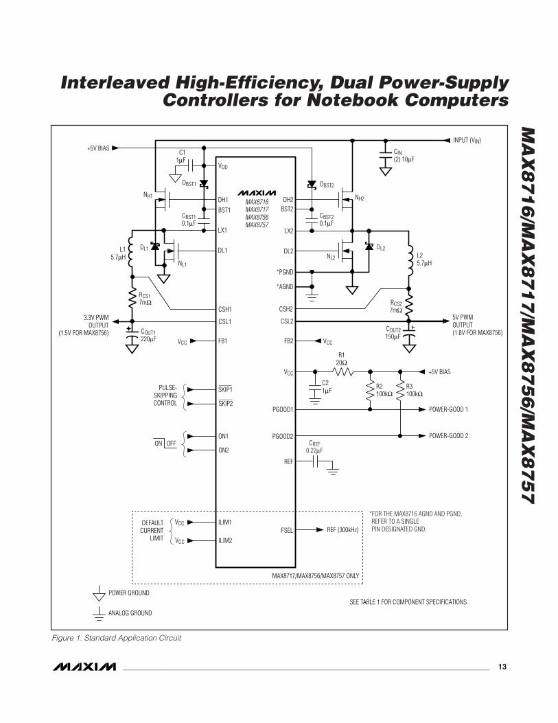
Detailed DescriptionThe MAX8716/MAX8717/MAX8756/MAX8757 StandardApplication Circuit (Figure 1) generates the 5V/5A and3.3V/5A typical of the main supplies in notebook com-puters. The input supply range is 6V to 24V. See Table 1for component selections, while Table 2 lists the compo-nent manufacturers.
The MAX8716/MAX8717/MAX8756/MAX8757 containtwo interleaved fixed-frequency, step-down controllersdesigned for low-voltage power supplies. The optimalinterleaved architecture guarantees out-of-phase oper-ation, which reduces the input capacitor ripple.
SMPS 5V Bias Supply (VCC and VDD)The MAX8716/MAX8717/MAX8756/MAX8757 switch-mode power supplies (SMPS) require a 5V bias supplyin addition to the high-power input supply (battery orAC adapter). VDD is the power rail for the MOSFET gatedrive, and VCC is the power rail for the IC. Connect theexternal 4.5V to 5.5V supply directly to VDD and con-nect VDD to VCC through an RC filter, as shown inFigure 1. The maximum supply current required is:
IBIAS = ICC + fSW (QG(NL1) + QG1(NH1) +QG2(NL2) +
QG2(NH2)) = 1.3mA to 40mA
where ICC is 1.3mA, fSW is the switching frequency,and QG_ are the MOSFET data sheet’s total gate-charge specification limits at VGS = 5V.
Pin Description (continued)
PIN
MAX8716MAX8717/MAX8756/MAX8757
NAME FUNCTION
14 16 DL2 Low-Side Gate-Driver Output for SMPS2. DL2 swings from PGND to VDD.
15 17 VDD Supply Voltage Input for the DL_ Gate Drivers. Connect to a 5V supply.
16 — GND Power and Analog Ground. Connect backside pad to GND.
— 18 PGND Power Ground
— 19 AGND Analog Ground. Connect backside pad to AGND.
17 20 DL1 Low-Side Gate-Driver Output for SMPS1. DL1 swings from PGND to VDD.
18 21 LX1Inductor Connection for SMPS1. Connect LX1 to the switched side of the inductor. LX1is the lower supply rail for the DH1 high-side gate driver.
19 22 DH1 High-Side Gate-Driver Output for SMPS1. DH1 swings from LX1 to BST1.
20 23 BST1Boost Flying Capacitor Connection for SMPS1. Connect to an external capacitor anddiode as shown in Figure 1. An optional resistor in series with BST1 allows the DH1 turn-on current to be adjusted.
21 24 CSH1Positive Current-Sense Input for SMPS1. Connect to the positive terminal of the current-sense element. Figure 8 describes two different current-sensing options.
22 25 CSL1Negative Current-Sense Input for SMPS1. Connect to the negative terminal of thecurrent-sense element. Figure 8 describes two different current-sensing options.
23 26 FB1Feedback Input for SMPS1. Connect FB1 to VCC for fixed 3.3V output for theMAX8716/MAX8717/MAX8757, or a fixed 1.5V for the MAX8756. In adjustable mode,FB1 regulates to 1V.
24 27 PGOOD1SMPS1 Open-Drain Power-Good Output. PGOOD1 is low when SMPS1 is more than10% below its regulation threshold, during soft-start, and in shutdown.
— 28 ILIM1
SMPS1 Peak Current-Limit Threshold Adjustment. Connect ILIM1 to VCC to enable thedefault 50mV current-limit threshold. In adjustable mode, the current-limit thresholdacross CSH1 and CSL1 is precisely 1/10 the voltage seen at ILIM1 over a 500mV to2.0V range. The logic threshold for switchover to the 50mV default value isapproximately VCC - 1V.
EP EP EP Exposed Pad. Connect exposed backside pad to analog ground.
MA
X8
71
6/M
AX
87
17
/MA
X8
75
6/M
AX
87
57
Interleaved High-Efficiency, Dual Power-SupplyControllers for Notebook Computers
______________________________________________________________________________________ 13
VDD
DH1
BST1
DL1
LX1
CSH1
CBST20.1μF
NH2
DL2
RCS27mΩ
L25.7μH
COUT2150μF
+5V BIAS
POWER-GOOD 1
POWER-GOOD 2
NL2
CBST10.1μF
NH1
NL1
RCS17mΩ
COUT1220μF
DL1L15.7μH
DBST1 DBST2
C11μF
+5V BIAS
3.3V PWMOUTPUT
(1.5V FOR MAX8756)
INPUT (VIN)
SEE TABLE 1 FOR COMPONENT SPECIFICATIONS.
FB1
POWER GROUND
ANALOG GROUND
MAX8716MAX8717MAX8756MAX8757
CIN(2) 10μF
REF (300kHz)
SKIP1
SKIP2
ILIM1
ILIM2
BST2
LX2
DL2
*PGND
*AGND
CSH2
CSL2
FB2
DH2
CSL1
DEFAULTCURRENT
LIMIT
ON1
ON2ON OFF
5V PWMOUTPUT(1.8V FOR MAX8756)
VCC
PGOOD1
R120Ω
C21μF
R2100kΩ
PGOOD2
FSEL
REF
R3100kΩ
VCC
PULSE-SKIPPINGCONTROL
VCC
VCC
VCC
CREF0.22μF
MAX8717/MAX8756/MAX8757 ONLY
*FOR THE MAX8716 AGND AND PGND, REFER TO A SINGLE PIN DESIGNATED GND.
Figure 1. Standard Application Circuit

MA
X8
71
6/M
AX
87
17
/MA
X8
75
6/M
AX
87
57
Interleaved High-Efficiency, Dual Power-SupplyControllers for Notebook Computers
14 ______________________________________________________________________________________
Reference (REF)The 2V reference is accurate to ±1.5% over tempera-ture and load, making REF useful as a precision systemreference. Bypass REF to GND with a 0.1µF or greaterceramic capacitor. The reference sources up to 50µAand sinks 10µA to support external loads.
SMPS Detailed DescriptionPower-on reset (POR) occurs when VCC rises aboveapproximately 2V, resetting the undervoltage, overvolt-age, and thermal-shutdown fault latches. The POR cir-cuit also ensures that the low-side drivers are drivenhigh until the SMPS controllers are activated. The VCCinput undervoltage-lockout (UVLO) circuitry inhibitsswitching if VCC is below the VCC UVLO threshold.
An internal soft-start gradually increases the regulationvoltage during startup to reduce the input surge cur-rents (see the Startup Waveforms in the TypicalOperating Characteristics).
COMPONENTMAX8716/MAX8717/MAX8757
5V/5A, 3.3V/5A, 300kHzMAX8716/MAX8717/MAX8757
5V/5A, 3.3V/5A, 500kHzMAX8756
1.8V/5A, 1.5V/5A, 300kHz
Input Voltage VIN = 7V to 24V VIN = 7V to 24V VIN = 7V to 24V
CIN, Input Capacitor(2) 10µF, 25V
Taiyo Yuden TMK432BJ106KM(2) 10µF, 25V
Taiyo Yuden TMK432BJ106KM(2) 10µF, 25V
Taiyo Yuden TMK432BJ106KM
COUT1, Output Capacitor220µF, 4V, 25mΩ
low-ESR capacitor,SANYO 4TPE220M
150µF, 4V, 25mΩlow-ESR capacitor,SANYO 4TPE150M
220µF, 4V, 18mΩlow-ESR capacitor,
SANYO 4TPE220MIC2
COUT2, Output Capacitor150µF, 6.3V, 25mΩlow-ESR capacitor,SANYO 6TPE150M
100µF, 6.3V, 25mΩlow-ESR capacitor,SANYO 6TPE100M
220µF, 4V, 18mΩlow-ESR capacitor,
SANYO 4TPE220MIC2
NH_ High-Side MOSFET
Fairchild SemiconductorFDS6612A
International RectifierIRF7807V
Fairchild SemiconductorFDS6612A
International RectifierIRF7807V
Fairchild SemiconductorFDS6612A
International RectifierIRF7807V
NL_ Low-Side MOSFET
Fairchild SemiconductorFDS6670S
International RectifierIRF7807VD1
Fairchild SemiconductorFDS6670S
International RectifierIRF7807VD1
Fairchild SemiconductorFDS6670S
International RectifierIRF7807VD1
DL_ Schottky Rectifier(if needed)
Nihon EC21QS03L2A, 30V, 0.45Vf
Nihon EC21QS03L2A, 30V, 0.45Vf
Nihon EC21QS03L2A, 30V, 0.45Vf
L_ Inductor5.7µH
Sumida CDEP105-5R7NC3.9µH
Sumida CDRH124-3R9NC3.1µH
Sumida CDRH125-3R1NC
RSENSE_
7mΩ ±1% 0.5W resistorIRC LR2010-01-R007F orDale WSL-2010-R007F
7mΩ ±1% 0.5W resistorIRC LR2010-01-R007F orDale WSL-2010-R007F
7mΩ ±1% 0.5W resistorIRC LR2010-01-R007F orDale WSL-2010-R007F
Table 1. Component Selection for Standard Applications
SUPPLIER WEBSITE
AVX www.avx.com
Central Semiconductor www.centralsemi.com
Coilcraft www.coilcraft.com
Coiltronics www.coiltronics.com
Fairchild Semiconductor www.fairchildsemi.com
International Rectifier www.irf.com
KEMET www.kemet.com
Panasonic www.panasonic.com/industrial
SANYO www.secc.co.jp
Sumida www.sumida.com
Taiyo Yuden www.t-yuden.com
TDK www.component.tdk.com
TOKO www.tokoam.com
Vishay (Dale, Siliconix) www.vishay.com
Table 2. Component Suppliers

MA
X8
71
6/M
AX
87
17
/MA
X8
75
6/M
AX
87
57
Interleaved High-Efficiency, Dual Power-SupplyControllers for Notebook Computers
______________________________________________________________________________________ 15
SMPS Enable Controls (ON1, ON2)ON1 and ON2 provide independent control of outputsoft-start and soft-shutdown. This allows flexible controlof startup and shutdown sequencing. The outputs canbe started simultaneously, sequentially, or indepen-dently. To provide sequential startup, connect ON_ ofone regulator to PGOOD_ of the other. For example,with ON1 connected to PGOOD2, OUT1 soft-starts afterOUT2 is in regulation. Drive ON_ low to clear the over-voltage, undervoltage, and thermal fault latches.
Soft-Start and Soft-ShutdownSoft-start begins when ON_ is driven high and REF is inregulation. During soft-start, the output is ramped up
from 0V to the final set voltage in 2ms. This reducesinrush current and provides a predictable ramp-up timefor power sequencing.
Soft-shutdown begins after ON_ goes low, an outputundervoltage fault occurs, or a thermal fault occurs.The two outputs are independent. A fault at one outputdoes not trigger shutdown of the other. During soft-shutdown the output is ramped down to 0V in 4ms,reducing negative inductor currents that can causenegative voltages on the output. At the end of soft-shut-down, DL_ is driven high until startup is again triggeredby a rising edge of ON_. The reference is turned offwhen both outputs have been shut down.
FB1
DH1
BST1
DL1
LX1
PWM1CONTROLLER
(FIGURE 3)
PGND
FBDECODE
(FIGURE 5)
FSEL
ILIM1
CSH1
CSL1
PGOOD1 POWER-GOOD ANDFAULT PROTECTION
(FIGURE 7)
INTE
RNAL
FB
FAUL
T
OSC
MAX8717/MAX8756/MAX8757VCC
REF
R
R2.0VREF GND
FB2
DH2
BST2
DL2
VDD
LX2
PWM2CONTROLLER
(FIGURE 3)
FBDECODE
(FIGURE 5)
ILIM2
CSH2
CSL2
PGOOD2POWER-GOOD ANDFAULT PROTECTION
(FIGURE 7)
INTE
RNAL
FB
FAUL
T
SKIP1
ON1
SKIP2
ON2
VDD
Figure 2. Functional Diagram

MA
X8
71
6/M
AX
87
17
/MA
X8
75
6/M
AX
87
57
Interleaved High-Efficiency, Dual Power-SupplyControllers for Notebook Computers
16 ______________________________________________________________________________________
Fixed-Frequency, Current-Mode PWM Controller
The heart of each current-mode PWM controller is amulti-input, open-loop comparator that sums two sig-nals: the output-voltage error signal with respect to thereference voltage and the slope-compensation ramp (Figure 3). The MAX8716/MAX8717/MAX8756/MAX8757 use a direct-summing configuration,approaching ideal cycle-to-cycle control over the out-put voltage without a traditional error amplifier and thephase shift associated with it. The MAX8716/MAX8717/MAX8756/MAX8757 use a relatively low loop gain,allowing the use of low-cost output capacitors. The lowloop gain results in the 0.1% typical load-regulationerror and helps reduce the output capacitor size andcost by shifting the unity-gain crossover frequency to alower level.
Frequency Selection (FSEL)The FSEL input selects the PWM mode switching fre-quency. Table 3 shows the switching frequency basedon the FSEL connection. High-frequency operation opti-mizes the application for the smallest component size,trading off efficiency due to higher switching losses.This may be acceptable in ultra-portable devices wherethe load currents are lower. Low-frequency operationoffers the best overall efficiency at the expense of com-ponent size and board space.
Forced-PWM ModeTo maintain low ripple fixed-frequency operation, driveSKIP_ high to put the output into forced-PWM mode.This disables the zero-crossing comparator and allowsnegative inductor current. During forced-PWM mode,
S
RQ
R
SQ
DH DRIVER
DL DRIVER
SLOPE COMP
OSC
FB
REF / 2
-1.2 x VLIMIT
AGND
SKIP
VLIMIT
3mV
CSL
CSH
SOFT-STARTSOFT-STOP
ON
SKIPDECODE
0.2 x VLIMIT0.1 x VLIMIT
(0.05 x VLIMIT FOR MAX8756)
Figure 3. PWM-Controller Functional Diagram
MA
X8
71
6/M
AX
87
17
/MA
X8
75
6/M
AX
87
57
Interleaved High-Efficiency, Dual Power-SupplyControllers for Notebook Computers
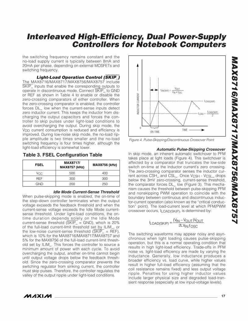
______________________________________________________________________________________ 17
the switching frequency remains constant and the no-load supply current is typically between 8mA and20mA per phase, depending on external MOSFETs andswitching frequency.
Light-Load Operation Control (SKIP_)The MAX8716/MAX8717/MAX8756/MAX8757 includeSKIP_ inputs that enable the corresponding outputs tooperate in discontinuous mode. Connect SKIP_ to GNDor REF as shown in Table 4 to enable or disable thezero-crossing comparators of either controller. Whenthe zero-crossing comparator is enabled, the controllerforces DL_ low when the current-sense inputs detectzero inductor current. This keeps the inductor from dis-charging the output capacitors and forces the con-troller to skip pulses under light-load conditions toavoid overcharging the output. During skip mode, theVDD current consumption is reduced and efficiency isimproved. During low-noise skip mode, the no-load rip-ple amplitude is two times smaller and the no-loadswitching frequency is four times higher, although thelight-load efficiency is somewhat lower.
Idle Mode Current-Sense ThresholdWhen pulse-skipping mode is enabled, the on-time ofthe step-down controller terminates when the outputvoltage exceeds the feedback threshold and when thecurrent-sense voltage exceeds the Idle Mode current-sense threshold. Under light-load conditions, the on-time duration depends solely on the Idle Modecurrent-sense threshold (SKIP_ = GND), which is 20%of the full-load current-limit threshold set by ILIM_, orthe low-noise current-sense threshold (SKIP_ = REF),which is 10% for the MAX8716/MAX8717/MAX8757 and5% for the MAX8756 of the full-load current-limit thresh-old set by ILIM_. This forces the controller to source aminimum amount of power with each cycle. To avoidovercharging the output, another on-time cannot beginuntil output voltage drops below the feedback thresh-old. Since the zero-crossing comparator prevents theswitching regulator from sinking current, the controllermust skip pulses. Therefore, the controller regulates thevalley of the output ripple under light-load conditions.
Automatic Pulse-Skipping CrossoverIn skip mode, an inherent automatic switchover to PFMtakes place at light loads (Figure 4). This switchover isaffected by a comparator that truncates the low-sideswitch on-time at the inductor current’s zero crossing.The zero-crossing comparator senses the inductor cur-rent across CSH_ and CSL_. Once VCSH - VCSL_ dropsbelow the 3mV zero-crossing, current-sense threshold,the comparator forces DL_ low (Figure 3). This mecha-nism causes the threshold between pulse-skipping PFMand nonskipping PWM operation to coincide with theboundary between continuous and discontinuous induc-tor-current operation (also known as the “critical conduc-tion” point). The load-current level at which PFM/PWMcrossover occurs, ILOAD(SKIP), is determined by:
The switching waveforms may appear noisy and asyn-chronous when light loading causes pulse-skippingoperation, but this is a normal operating condition thatresults in high light-load efficiency. Trade-offs in PFMnoise vs. light-load efficiency are made by varying theinductance. Generally, low inductance produces abroader efficiency vs. load curve, while higher valuesresult in higher full-load efficiency (assuming that thecoil resistance remains fixed) and less output voltageripple. Penalties for using higher inductor valuesinclude larger physical size and degraded load-tran-sient response (especially at low input-voltage levels).
IV V V
LVLOAD SKIPIN OUT OUT
IN OSC( )
( )= −ƒ2
FSELMAX8717/
MAX8757 (kHz)MAX8756 (kHz)
VCC 500 400
REF 300 300
GND 200 250
Table 3. FSEL Configuration Table
tON(SKIP) = VOUT
VIN x fOSC
INDU
CTOR
CUR
RENT
ILOAD(SKIP)
TIMEON-TIME
0
ILOAD = ILOAD(SKIP)
2
Figure 4. Pulse-Skipping/Discontinuous Crossover Point

MA
X8
71
6/M
AX
87
17
/MA
X8
75
6/M
AX
87
57
Interleaved High-Efficiency, Dual Power-SupplyControllers for Notebook Computers
18 ______________________________________________________________________________________
Output VoltageDC output accuracy specifications in the ElectricalCharacteristics refer to the error comparator’s thresh-old. When the inductor continuously conducts, theMAX8716/MAX8717/MAX8756/MAX8757 regulate thepeak of the output ripple, so the actual DC output volt-age is lower than the slope-compensated trip level by50% of the output ripple voltage. For PWM operation(continuous conduction), the output voltage is accu-rately defined by the following equation:
where VNOM is the nominal output voltage, ASLOPEequals 1%, and VRIPPLE is the output ripple voltage(VRIPPLE = RESR x ΔIINDUCTOR as described in theOutput Capacitor Selection section).
In discontinuous conduction (IOUT < ILOAD(SKIP)), theMAX8716/MAX8717/MAX8756/MAX8757 regulate thevalley of the output ripple, so the output voltage has a DCregulation level higher than the error-comparator thresh-old. For PFM operation (discontinuous conduction), theoutput voltage is approximately defined by the followingequation:
where VNOM is the nominal output voltage, fOSC is themaximum switching frequency set by the internal oscil-lator, fSW is the actual switching frequency, and IIDLE isthe Idle Mode inductor current when pulse skipping.
V V I ROUT PFM NOMSW
OSCIDLE ESR( ) = + ƒ
ƒ⎛⎝⎜
⎞⎠⎟
12
V VA V V
VV
OUT PWM NOMSLOPE IN NOM
IN
RIPPLE( )
( )= − −⎛⎝⎜
⎞⎠⎟
− ⎛⎝⎜
⎞⎠⎟
12
SKIP_ MODE COMMENTS
VCCForced-PWM
mode
Fixed-frequency operation.Constant output ripple voltage.Able to source and sink current.
GND Skip modeHigh efficiency at light loads.Source-only applications.
REFLow-noiseskip mode
Good efficiency at light loads.(VIDLE / VLN) times smaller no-loadripple and (VIDLE / VLN)2 times higherfrequency compared with skip mode.Source-only applications.
Table 4. SKIP_ Configuration Table
MODE CONDITION COMMENT
Power-Up VCC UVLO
DL_ tracks VCC as VCC rises from 0V to +5V.When ON_ is low, DL_ tracks VCC as VCC falls.When ON_ is high, DL_ is forced low as VCC falls below the3.95V (typ) falling UVLO threshold. DL_ is forced high whenVCC falls below 1V (typ).
Run ON1 or ON2 enabled Normal operation.
Output OvervoltageProtection (OVP)
MAX8716/MAX8717/MAX8756 Only
Either output > 115% of nominal level
When the overvoltage (OV) comparator trips, the faulted sidesets the OV latch, forcing PGOOD_ low and DL_ high. Theother controller is not affected.The OV latch is cleared by cycling VCC below 1V or cyclingthe respective ON_ pin.
Output UndervoltageProtection (UVP)
Either output < 70% of nominal level,UVP is enabled 6144 clock cycles(1/fOSC) after the output is enabled
(ON_ going high)
When the undervoltage (UV) comparator trips, the faultedside sets the UV latch, forcing PGOOD_ low and initiating thesoft-shutdown sequence by pulsing only DL_. DL_ goes highafter soft-shutdown. The other controller is not affected.The UV latch is cleared by cycling VCC below 1V or cyclingthe respective ON_ pin.
Shutdown ON1 and ON2 are driven lowDL_ stays high after soft-shutdown is completed.All circuitry is shut down.
Thermal Shutdown TJ > +160°CExited by POR or cycling ON1 and ON2.DL1 and DL2 remain high.
Table 5. Operating Modes Truth Table

MA
X8
71
6/M
AX
87
17
/MA
X8
75
6/M
AX
87
57
Interleaved High-Efficiency, Dual Power-SupplyControllers for Notebook Computers
______________________________________________________________________________________ 19
Adjustable/Fixed Output Voltages (Dual-Mode Feedback)
Connect FB1 and FB2 to VCC to enable the fixed SMPSoutput voltages (3.3V and 5V, respectively, for theMAX8716/MAX8717/MAX8757, and 1.5V and 1.8V forthe MAX8756, respectively), set by a preset, internalresistive voltage-divider connected between CSL_ andanalog ground. See Figure 5. Connect a resistive volt-age-divider at FB_ between CSL_ and GND to adjustthe respective output voltage between 1V and 5.5V.Choose R2 (resistance from FB to AGND) to be approx-imately 10kΩ and solve for R1 (resistance from OUT toFB) using the equation:
where VFB_ = 1V nominal.
Current-Limit Protection (ILIM_)The current-limit circuit uses differential current-senseinputs (CSH_ and CSL_) to limit the peak inductor cur-rent. If the magnitude of the current-sense signalexceeds the current-limit threshold, the PWM controllerturns off the high-side MOSFET (Figure 3). At the nextrising edge of the internal oscillator, the PWM controllerdoes not initiate a new cycle unless the current-sensesignal drops below the current-limit threshold. Theactual maximum load current is less than the peak cur-rent-limit threshold by an amount equal to half of the
inductor ripple current. Therefore, the maximum loadcapability is a function of the current-sense resistance,inductor value, switching frequency, and duty cycle(VOUT / VIN).
In forced-PWM mode, the MAX8716/MAX8717/MAX8756/MAX8757 also implement a negative currentlimit to prevent excessive reverse inductor currentswhen VOUT is sinking current. The negative current-limitthreshold is set to approximately -120% of the positivecurrent limit and tracks the positive current limit whenILIM is adjusted.
Connect ILIM_ to VCC for the 50mV default threshold, oradjust the current-limit threshold with an external resis-tor-divider at ILIM_. Use a 2µA to 20µA divider currentfor accuracy and noise immunity. The current-limitthreshold adjustment range is from 50mV to 200mV. Inthe adjustable mode, the current-limit threshold voltageequals precisely 1/10 the voltage seen at ILIM_. Thelogic threshold for switchover to the 50mV default valueis approximately VCC - 1V.
Carefully observe the PCB layout guidelines to ensurethat noise and DC errors do not corrupt the differentialcurrent-sense signals seen by CSH_ and CSL_. Placethe IC close to the sense resistor with short, directtraces, making a Kelvin-sense connection to the cur-rent-sense resistor.
MOSFET Gate Drivers (DH_, DL_)The DH_ and DL_ drivers are optimized for drivingmoderate-sized high-side, and larger low-side powerMOSFETs. This is consistent with the low duty factorseen in notebook applications, where a large VIN -VOUT differential exists. The high-side gate drivers(DH_) source and sink 2A, and the low-side gate dri-vers (DL_) source 1.7A and sink 3.3A. This ensuresrobust gate drive for high-current applications. TheDH_ floating high-side MOSFET drivers are powered bydiode-capacitor charge pumps at BST_ (Figure 6) whilethe DL_ synchronous-rectifier drivers are powereddirectly by the external 5V supply (VDD).
Adaptive dead-time circuits monitor the DL_ and DH_ dri-vers and prevent either FET from turning on until the otheris fully off. The adaptive driver dead-time allows operationwithout shoot-through with a wide range of MOSFETs,minimizing delays and maintaining efficiency. There mustbe a low-resistance, low-inductance path from the DL_and DH_ drivers to the MOSFET gates for the adaptivedead-time circuits to work properly; otherwise, the sensecircuitry in the MAX8716/MAX8717/MAX8756/MAX8757interprets the MOSFET gates as “off” while charge actuallyremains. Use very short, wide traces (50 mils to 100 milswide if the MOSFET is 1in from the driver).
R RV
VOUT
FB1 2 1= −
⎛
⎝⎜
⎞
⎠⎟
_
_
CSL
TO ERRORAMPLIFIER
FB
2V
FIXED OUTPUTFB = VCC
ADJUSTABLEOUTPUT
Figure 5. Dual Mode Feedback Decoder

MA
X8
71
6/M
AX
87
17
/MA
X8
75
6/M
AX
87
57
Interleaved High-Efficiency, Dual Power-SupplyControllers for Notebook Computers
20 ______________________________________________________________________________________
The internal pulldown transistor that drives DL_ low isrobust, with a 0.6Ω (typ) on-resistance. This helps pre-vent DL_ from being pulled up due to capacitive cou-pling from the drain to the gate of the low-side MOSFETswhen the inductor node (LX_) quickly switches fromground to VIN. Applications with high input voltages andlong inductive driver traces may require additional gate-to-source capacitance to ensure fast-rising LX_ edgesdo not pull up the low-side MOSFETs gate, causingshoot-through currents. The capacitive couplingbetween LX_ and DL_ created by the MOSFET’s gate-to-drain capacitance (CRSS), gate-to-source capacitance(CISS - CRSS), and additional board parasitics should notexceed the following minimum threshold:
Variation of the threshold voltage may cause problemsin marginal designs. Alternatively, adding a resistorless than 10Ω in series with BST_ may remedy theproblem by increasing the turn-on time of the high-sideMOSFET without degrading the turn-off time (Figure 6).
Power-Good Output (PGOOD_)PGOOD_ is the open-drain output of a comparator thatcontinuously monitors each SMPS output voltage forovervoltage and undervoltage conditions. PGOOD_ isactively held low in shutdown (ON_ = GND), soft-start,and soft-shutdown. Once the analog soft-start termi-nates, PGOOD_ becomes high impedance as long asthe output is above 90% of the nominal regulation volt-age set by FB_. PGOOD_ goes low once the outputdrops 10% below its nominal regulation point, an outputovervoltage fault occurs, or ON_ is pulled low. For alogic-level PGOOD_ output voltage, connect an exter-nal pullup resistor between PGOOD_ and +5V or +3.3V.A 100kΩ pullup resistor works well in most applications.
Fault ProtectionOutput Overvoltage Protection
(MAX8716/MAX8717/MAX8756 Only)If the output voltage of either SMPS rises above 115%of its nominal regulation voltage, the correspondingcontroller sets its overvoltage fault latch, pulls PGOOD_low, and forces DL_ high for the corresponding SMPScontroller. The other controller is not affected. If thecondition that caused the overvoltage persists (such asa shorted high-side MOSFET), the battery fuse willblow. Cycle VCC below 1V or toggle ON_ to clear theovervoltage fault latch and restart the SMPS controller.
V VCCGS TH IN
RSS
ISS( ) >
⎛⎝⎜
⎞⎠⎟
MAX8716MAX8717MAX8756MAX8757
VDD
BST
DH
LX
(RBST)*
(CNL)*
DBST
CBST
CBYP
INPUT (VIN)
NH
L
DL
PGND
NL
(RBST)* OPTIONAL—THE RESISTOR LOWERS EMI BY DECREASINGTHE SWITCHING-NODE RISE TIME.(CNL)* OPTIONAL—THE CAPACITOR REDUCES LX TO DL CAPACITIVECOUPLING THAT CAN CAUSE SHOOT-THROUGH CURRENTS.
VDD
Figure 6. Optional Gate-Driver Circuitry
POWER-GOOD
FAULT
0.9 xINT REF_
1.15 xINT REF_
0.7 xINT REF_
FAULTLATCH
POWER-GOOD
FAULTPROTECTION
INTERNAL FB
TIMER
POR
Figure 7. Power-Good and Fault Protection
MA
X8
71
6/M
AX
87
17
/MA
X8
75
6/M
AX
87
57
Interleaved High-Efficiency, Dual Power-SupplyControllers for Notebook Computers
______________________________________________________________________________________ 21
Output Undervoltage ProtectionIf the output voltage of either SMPS falls below 70% ofits regulation voltage, the corresponding controller setsits undervoltage fault latch, pulls PGOOD_ low, andbegins soft-shutdown for the corresponding SMPS con-troller by pulsing DL_. DH_ remains off during the soft-shutdown sequence initiated by an unvervoltage fault.The other controller is not affected. After soft-shutdownhas completed, the MAX8716/MAX8717/MAX8756/MAX8757 force DL_ high and DH_ low. Cycle VCCbelow 1V or toggle ON_ to clear the undervoltage faultlatch and restart the SMPS controller.
VCC POR and UVLOPower-on reset (POR) occurs when VCC rises aboveapproximately 2V, resetting the fault latch and prepar-ing the PWM for operation. VCC undervoltage-lockout(UVLO) circuitry inhibits switching, forces PGOOD_low, and forces the DL_ gate drivers low.
If VCC drops low enough to trip the UVLO comparatorwhile ON_ is high, the MAX8716/MAX8717/MAX8756/MAX8757 immediately force DH_ and DL_ low on bothcontrollers. The output discharges to 0V at a ratedependent on the load and the total output capaci-tance. This prevents negative output voltages, eliminat-ing the need for a Schottky diode to GND at the output.
Thermal Fault ProtectionThe MAX8716/MAX8717/MAX8756/MAX8757 feature athermal fault-protection circuit. When the junction tem-perature rises above +160°C, a thermal sensor sets thefault latches, pulls PGOOD low, and shuts down bothSMPS controllers using the soft-shutdown sequence(see the Sort-Start and Soft-Shutdown section). CycleVCC below 1V or toggle ON1 and ON2 to clear the faultlatches and restart the controllers after the junctiontemperature cools by 15°C.
Design ProcedureFirmly establish the input voltage range and maximumload current before choosing a switching frequencyand inductor operating point (ripple-current ratio). Theprimary design trade-off lies in choosing a good switch-ing frequency and inductor operating point, and the fol-lowing four factors dictate the rest of the design:
• Input Voltage Range. The maximum value (VIN(MAX))must accommodate the worst-case, high AC-adaptervoltage. The minimum value (VIN(MIN)) must accountfor the lowest battery voltage after drops due to con-nectors, fuses, and battery selector switches. If thereis a choice at all, lower input voltages result in betterefficiency.
• Maximum Load Current. There are two values toconsider. The peak load current (ILOAD(MAX)) deter-mines the instantaneous component stresses and fil-tering requirements and thus drives output capacitorselection, inductor saturation rating, and the designof the current-limit circuit. The continuous load cur-rent (ILOAD) determines the thermal stresses and thusdrives the selection of input capacitors, MOSFETs,and other critical heat-contributing components.
• Switching Frequency. This choice determines thebasic trade-off between size and efficiency. Theoptimal frequency is largely a function of maximuminput voltage, due to MOSFET switching losses thatare proportional to frequency and VIN2. The opti-mum frequency is also a moving target, due to rapidimprovements in MOSFET technology that are mak-ing higher frequencies more practical.
• Inductor Operating Point. This choice providestrade-offs between size vs. efficiency and transientresponse vs. output ripple. Low inductor values pro-vide better transient response and smaller physicalsize, but also result in lower efficiency and higheroutput ripple due to increased ripple currents. Theminimum practical inductor value is one that causesthe circuit to operate at the edge of critical conduc-tion (where the inductor current just touches zerowith every cycle at maximum load). Inductor valueslower than this grant no further size-reduction bene-fit. The optimum operating point is usually foundbetween 20% and 50% ripple current. When pulse-skipping (SKIP low and light loads), the inductorvalue also determines the load-current value atwhich PFM/PWM switchover occurs.
Inductor SelectionThe switching frequency and inductor operating pointdetermine the inductor value as follows:
For example: ILOAD(MAX) = 5A, VIN = 12V, VOUT = 5V,fOSC = 300kHz, 30% ripple current or LIR = 0.3:
Find a low-loss inductor having the lowest possible DCresistance that fits in the allotted dimensions. Mostinductor manufacturers provide inductors in standardvalues, such as 1.0µH, 1.5µH, 2.2µH, 3.3µH, etc. Also
LV V V
V kHz AH= × −
× × ×=5 12 5
12 300 5 0 36 50
( ).
. μ
LV V V
V I LIROUT IN OUT
IN OSC LOAD MAX= −
ƒ( )
( )

MA
X8
71
6/M
AX
87
17
/MA
X8
75
6/M
AX
87
57
Interleaved High-Efficiency, Dual Power-SupplyControllers for Notebook Computers
22 ______________________________________________________________________________________
look for nonstandard values, which can provide a bettercompromise in LIR across the input voltage range. Ifusing a swinging inductor (where the no-load induc-tance decreases linearly with increasing current), evalu-ate the LIR with properly scaled inductance values. Forthe selected inductance value, the actual peak-to-peakinductor ripple current (ΔIINDUCTOR) is defined by:
Ferrite cores are often the best choice, although pow-dered iron is inexpensive and can work well at 200kHz.The core must be large enough not to saturate at thepeak inductor current (IPEAK):
Transient ResponseThe inductor ripple current also impacts transient-response performance, especially at low VIN - VOUT dif-ferentials. Low inductor values allow the inductorcurrent to slew faster, replenishing charge removedfrom the output filter capacitors by a sudden load step.The total output voltage sag is the sum of the voltagesag while the inductor is ramping up and the voltagesag before the next pulse can occur:
where DMAX is maximum duty factor (see the ElectricalCharacteristics), T is the switching period (1 / fOSC), andΔT equals VOUT / VIN x T when in PWM mode, or L x 0.2x IMAX / (VIN - VOUT) when in skip mode. The amount ofovershoot during a full-load to no-load transient due tostored inductor energy can be calculated as:
Setting the Current LimitThe minimum current-limit threshold must be greatenough to support the maximum load current when thecurrent limit is at the minimum tolerance value. Thepeak inductor current occurs at ILOAD(MAX) plus halfthe ripple current; therefore:
where ILIMIT_ equals the minimum current-limit thresh-old voltage divided by the current-sense resistance(RSENSE). For the 50mV default setting, the minimumcurrent-limit threshold is 50mV.
Connect ILIM_ to VCC for a default 50mV current-limitthreshold. In adjustable mode, the current-limit thresh-old is precisely 1/10 the voltage seen at ILIM_. For anadjustable threshold, connect a resistive divider fromREF to analog ground (GND) with ILIM_ connected tothe center tap. The external 500mV to 2V adjustmentrange corresponds to a 50mV to 200mV current-limitthreshold. When adjusting the current limit, use 1% tol-erance resistors and a divider current of approximately10µA to prevent significant inaccuracy in the current-limit tolerance.
The current-sense method (Figure 8) and magnitudedetermines the achievable current-limit accuracy andpower loss. Typically, higher current-sense limits pro-vide tighter accuracy, but also dissipate more power.Most applications employ a current-limit threshold(VLIM) of 50mV to 100mV, so the sense resistor can bedetermined by:
RSENSE_ = VLIM_ / ILIM_
For the best current-sense accuracy and overcurrentprotection, use a 1% tolerance current-sense resistorbetween the inductor and output as shown in Figure 8a.This configuration constantly monitors the inductor cur-rent, allowing accurate current-limit protection.
Alternatively, high-power applications that do notrequire highly accurate current-limit protection mayreduce the overall power dissipation by connecting aseries RC circuit across the inductor (Figure 8b) with anequivalent time constant:
where RL is the inductor’s series DC resistance. In thisconfiguration, the current-sense resistance equals theinductor’s DC resistance (RSENSE = RL). Use the worst-case inductance and RL values provided by the induc-tor manufacturer, adding some margin for theinductance drop over temperature and load.
LR
C RL
EQ EQ= ×
I II
LIMIT LOAD MAXINDUCTOR> + ⎛
⎝⎜⎞⎠⎟( )
Δ2
VI L
C VSOARLOAD MAX
OUT OUT≈
( )( )Δ 2
2
VL I
C V D V
I T T
CSAGLOAD MAX
OUT IN MAX OUT
LOAD MAX
OUT=
× −+
−( )
( )
( )( ) ( )Δ Δ Δ2
2
I II
PEAK LOAD MAXINDUCTOR= +( )
Δ2
ΔIV V V
V LINDUCTOROUT IN OUT
IN OSC= −
ƒ( )

MA
X8
71
6/M
AX
87
17
/MA
X8
75
6/M
AX
87
57
Interleaved High-Efficiency, Dual Power-SupplyControllers for Notebook Computers
______________________________________________________________________________________ 23
Output Capacitor SelectionThe output filter capacitor must have low enough equiv-alent series resistance (ESR) to meet output ripple andload-transient requirements, yet have high enough ESRto satisfy stability requirements. The output capaci-tance must be high enough to absorb the inductorenergy while transitioning from full-load to no-load con-ditions without tripping the overvoltage fault protection.When using high-capacitance, low-ESR capacitors (seethe Output-Capacitor Stability Considerations section),the filter capacitor’s ESR dominates the output voltageripple. So the output capacitor’s size depends on themaximum ESR required to meet the output-voltage-rip-ple (VRIPPLE(P-P)) specifications:
VRIPPLE(P-P) = RESRILOAD(MAX)LIR
In Idle Mode, the inductor current becomes discontinu-ous, with peak currents set by the idle-mode current-sense threshold (VIDLE = 0.2VLIMIT). In Idle Mode, theno-load output ripple can be determined as follows:
The actual capacitance value required relates to thephysical size needed to achieve low ESR, as well as tothe chemistry of the capacitor technology. Thus, thecapacitor is usually selected by ESR and voltage ratingrather than by capacitance value (this is true of tanta-lums, OS-CONs, polymers, and other electrolytics).When using low-capacity filter capacitors, such asceramic capacitors, size is usually determined by thecapacity needed to prevent VSAG and VSOAR fromcausing problems during load transients. Generally,once enough capacitance is added to meet the over-shoot requirement, undershoot at the rising load edgeis no longer a problem (see the VSAG and VSOAR equa-tions in the Transient Response section). However, low-capacity filter capacitors typically have high-ESR zerosthat may effect the overall stability (see the Output-Capacitor Stability Considerations section).
VV RRRIPPLE P PIDLE ESR
SENSE( )− =
MAX8716MAX8717MAX8756MAX8757
COUT
INPUT (VIN)
INDUCTORCIN
b) LOSSLESS INDUCTOR SENSING
CSL_
CSH_
PGND
DL_
DH_
LX_
CEQREQ
RBIAS = REQ
MAX8716MAX8717MAX8756MAX8757
COUT
INPUT (VIN)
NH
NL
NH
NL
L
CIN
DL
DL
a) OUTPUT SERIES RESISTOR SENSING
PGND
DL_
DH_
LX_
CSL_
CSH_
RSENSE
Figure 8. Current-Sense Configurations

MA
X8
71
6/M
AX
87
17
/MA
X8
75
6/M
AX
87
57
Interleaved High-Efficiency, Dual Power-SupplyControllers for Notebook Computers
24 ______________________________________________________________________________________
Output-Capacitor Stability ConsiderationsStability is determined by the value of the ESR zero rel-ative to the switching frequency. The boundary of insta-bility is given by the following equation:
where:
For a typical 300kHz application, the ESR zero frequen-cy must be well below 95kHz, preferably below 50kHz.Tantalum and OS-CON capacitors in widespread useat the time of publication have typical ESR zero fre-quencies of 25kHz. In the design example used forinductor selection, the ESR needed to support 25mVP-Pripple is 25mV/1.5A = 16.7mΩ. One 220µF/4V SANYOpolymer (TPE) capacitor provides 15mΩ (max) ESR.This results in a zero at 48kHz, well within the boundsof stability.
For low input-voltage applications where the duty cycleexceeds 50% (VOUT / VIN ≥ 50%), the output ripplevoltage should not be greater than twice the internalslope-compensation voltage:
VRIPPLE ≤ 0.02 x VOUT
where VRIPPLE equals ΔIINDUCTOR x RESR. The worst-case ESR limit occurs when VIN = 2 x VOUT, so theabove equation can be simplified to provide the follow-ing boundary condition:
RESR ≤ 0.04 x L x ƒOSC
Do not put high-value ceramic capacitors directlyacross the feedback sense point without taking precau-tions to ensure stability. Large ceramic capacitors canhave a high-ESR zero frequency and cause erratic,unstable operation. However, it is easy to add enoughseries resistance by placing the capacitors a couple ofinches downstream from the feedback sense point,which should be as close as possible to the inductor.
Unstable operation manifests itself in two related butdistinctly different ways: short/long pulses or cycleskipping resulting in a lower switching frequency.Instability occurs due to noise on the output or becausethe ESR is so low that there is not enough voltage rampin the output voltage signal. This “fools” the error com-parator into triggering too early or skipping a cycle.Cycle skipping is more annoying than harmful, resultingin nothing worse than increased output ripple.However, it can indicate the possible presence of loopinstability due to insufficient ESR. Loop instability canresult in oscillations at the output after line or loadsteps. Such perturbations are usually damped, but can
cause the output voltage to rise above or fall below thetolerance limits.
The easiest method for checking stability is to apply avery fast zero-to-max load transient and carefullyobserve the output-voltage-ripple envelope for over-shoot and ringing. It can help to simultaneously monitorthe inductor current with an AC current probe. Do notallow more than one cycle of ringing after the initialstep-response under/overshoot.
Input Capacitor SelectionThe input capacitor must meet the ripple-currentrequirement (IRMS) imposed by the switching currents.For an out-of-phase regulator, the total RMS current inthe input capacitor is a function of the load currents,the input currents, the duty cycles, and the amount ofoverlap as defined in Figure 9.
The 40/60 optimal interleaved architecture of theMAX8716/MAX8717/MAX8756/MAX8757 allows theinput voltage to go as low as 8.3V before the dutycycles begin to overlap. This offers improved efficiencyover a regular 180° out-of-phase architecture where theduty cycles begin to overlap below 10V. Figure 9
ƒ =ESRESR OUTR Cπ
12
ƒƒ
≤ESRSWπ
INPUT CAPACITOR RMS CURRENTvs. INPUT VOLTAGE
VIN (V)
I RM
S (A
)
181612 14108
0.5
1.0
1.5
2.0
2.5
3.0
3.5
4.0
4.5
5.0
06 20
IN PHASE
5V/5A AND 3.3V/5A
50/50 INTERLEAVING
40/60 OPTIMALINTERLEAVING
INPUT RMS CURRENT FOR INTERLEAVED OPERATION
INPUT RMS CURRENT FOR SINGLE-PHASE OPERATION
(IOUT1 - IIN)2 (DLX1 - DOL) + (IOUT2 - IIN)2 (DLX2 - DOL) + (IOUT1 + IOUT2 - IIN)2 DOL + IIN2 (1 - DLX1 - DLX2 + DOL)
DLX1 =
VOUT (VIN - VOUT)VIN
IRMS = ILOAD
DOL = DUTY-CYCLE OVERLAP FRACTION VOUT1 VIN
VOUT1 IOUT1 + VOUT2 IOUT2 VIN
DLX2 = VOUT2 VIN
( )
IIN =
IRMS =
Figure 9. Input RMS Current

MA
X8
71
6/M
AX
87
17
/MA
X8
75
6/M
AX
87
57
Interleaved High-Efficiency, Dual Power-SupplyControllers for Notebook Computers
______________________________________________________________________________________ 25
shows the input-capacitor RMS current vs. input volt-age for an application that requires 5V/5A and 3.3V/5A.This shows the improvement of the 40/60 optimal inter-leaving over 50/50 interleaving and in-phase operation.
For most applications, nontantalum chemistries (ceramic,aluminum, or OS-CON) are preferred due to their resis-tance to power-up surge currents typical of systemswith a mechanical switch or connector in series with theinput. Choose a capacitor that has less than 10°C tem-perature rise at the RMS input current for optimal relia-bility and lifetime.
Power MOSFET SelectionMost of the following MOSFET guidelines focus on thechallenge of obtaining high load-current capabilitywhen using high-voltage (> 20V) AC adapters. Low-current applications usually require less attention.
The high-side MOSFET (NH) must be able to dissipatethe resistive losses plus the switching losses at bothVIN(MIN) and VIN(MAX). Ideally, the losses at VIN(MIN)should be roughly equal to the losses at VIN(MAX), withlower losses in between. If the losses at VIN(MIN) aresignificantly higher, consider increasing the size of NH.Conversely, if the losses at VIN(MAX) are significantlyhigher, consider reducing the size of NH. If VIN doesnot vary over a wide range, optimum efficiency isachieved by selecting a high-side MOSFET (NH) thathas conduction losses equal to the switching losses.
Choose a low-side MOSFET (NL) that has the lowestpossible on-resistance (RDS(ON)), comes in a moder-ate-sized package (i.e., 8-pin SO, DPAK, or D2PAK),and is reasonably priced. Ensure that theMAX8716/MAX8717/MAX8756/MAX8757 DL_ gate dri-ver can supply sufficient current to support the gatecharge and the current injected into the parasitic drain-to-gate capacitor caused by the high-side MOSFETturning on; otherwise, cross-conduction problems mayoccur. Switching losses are not an issue for the low-side MOSFET since it is a zero-voltage switched devicewhen used in the step-down topology.
Power MOSFET DissipationWorst-case conduction losses occur at the duty-factorextremes. For the high-side MOSFET (NH), the worst-case power dissipation due to resistance occurs atminimum input voltage:
Generally, use a small high-side MOSFET to reduceswitching losses at high input voltages. However, theRDS(ON) required to stay within package power-dissi-pation limits often limits how small the MOSFET can be.
The optimum occurs when the switching losses equalthe conduction (RDS(ON)) losses. High-side switchinglosses do not become an issue until the input is greaterthan approximately 15V.
Calculating the power dissipation in high-sideMOSFETs (NH) due to switching losses is difficult, sinceit must allow for difficult-to-quantify factors that influ-ence the turn-on and turn-off times. These factorsinclude the internal gate resistance, gate charge,threshold voltage, source inductance, and PCB layoutcharacteristics. The following switching-loss calculationprovides only a very rough estimate and is no substi-tute for breadboard evaluation, preferably includingverification using a thermocouple mounted on NH:
where COSS is the NH, MOSFET's output capacitance,QG(SW)2, is the change needed to turn on the NH MOSFET, and IGATE is the peak gate-drivesource/sink current (1A typ).
Switching losses in the high-side MOSFET can becomea heat problem when maximum AC adapter voltagesare applied, due to the squared term in the switching-loss equation (C x VIN2 x fSW). If the high-side MOSFETchosen for adequate RDS(ON) at low battery voltagesbecomes extraordinari ly hot when subjected toVIN(MAX), consider choosing another MOSFET withlower parasitic capacitance.
For the low-side MOSFET (NL), the worst-case powerdissipation always occurs at maximum battery voltage:
The absolute worst case for MOSFET power dissipationoccurs under heavy-overload conditions that aregreater than ILOAD(MAX) but are not high enough toexceed the current limit and cause the fault latch to trip.To protect against this possibility, “overdesign” the cir-cuit to tolerate:
where ILIMIT is the peak current allowed by the current-limit circuit, including threshold tolerance and sense-resistance variation. The MOSFETs must have arelatively large heatsink to handle the overload powerdissipation.
I II
LOAD LIMITINDUCTOR= − ⎛
⎝⎜⎞⎠⎟
Δ2
PD N RESISTIVEV
VI RL
OUT
IN MAXLOAD DS ON( ) ( )
( )( )= −
⎛
⎝⎜
⎞
⎠⎟
⎡
⎣⎢⎢
⎤
⎦⎥⎥
1 2
PD (N SWITCHING)
V I f Q
IC V f
2
H
IN(MAX) LOAD SW
TOTAL
G(SW)
GATE
OSS IN2
SW
=
⎛
⎝⎜⎞
⎠⎟⎛
⎝⎜⎞
⎠⎟+
η
PD N RESISTIVEVV
I RHOUT
INLOAD DS ON( ) ( ) ( )= 2

MA
X8
71
6/M
AX
87
17
/MA
X8
75
6/M
AX
87
57
Interleaved High-Efficiency, Dual Power-SupplyControllers for Notebook Computers
26 ______________________________________________________________________________________
Choose a Schottky diode (DL) with a forward-voltagedrop low enough to prevent the low-side MOSFET’sbody diode from turning on during the dead time. As ageneral rule, select a diode with a DC current ratingequal to 1/3 the load current. This diode is optional andcan be removed if efficiency is not critical.
Boost CapacitorsThe boost capacitors (CBST) must be selected largeenough to handle the gate-charging requirements ofthe high-side MOSFETs. Typically, 0.1µF ceramiccapacitors work well for low-power applications drivingmedium-sized MOSFETs. However, high-current appli-cations driving large, high-side MOSFETs require boostcapacitors larger than 0.1µF. For these applications,select the boost capacitors to avoid discharging thecapacitor more than 200mV while charging the high-side MOSFETs’ gates:
where QGATE is the total gate charge specified in thehigh-side MOSFET’s data sheet. For example, assumethe FDS6612A n-channel MOSFET is used on the highside. According to the manufacturer’s data sheet, a sin-gle FDS6612A has a maximum gate charge of 13nC(VGS = 5V). Using the above equation, the requiredboost capacitance would be:
Selecting the closest standard value, this examplerequires a 0.1µF ceramic capacitor.
Applications InformationDuty-Cycle Limits
Minimum Input VoltageThe minimum input operating voltage (dropout voltage)is restricted by the maximum duty-cycle specification(see the Electrical Characteristics table). For the bestdropout performance, use the slowest switching-fre-quency setting (FSEL = GND). However, keep in mindthat the transient performance gets worse as the step-down regulators approach the dropout voltage, so bulkoutput capacitance must be added (see the voltagesag and soar equations in the Design Procedure sec-tion). The absolute point of dropout occurs when theinductor current ramps down during the off-time(ΔIDOWN) as much as it ramps up during the on-time
(ΔIUP). This results in a minimum operating voltagedefined by the following equation:
where VCHG and VDIS are the parasitic voltage drops inthe charge and discharge paths, respectively. A rea-sonable minimum value for h is 1.5, while the absoluteminimum input voltage is calculated with h = 1.
Maximum Input VoltageThe MAX8716/MAX8717/MAX8756/MAX8757 controllerincludes a minimum on-time specification, which deter-mines the maximum input operating voltage that main-tains the selected switching frequency (see theElectrical Characteristics table). Operation above thismaximum input voltage results in pulse-skipping opera-tion, regardless of the operating mode selected bySKIP. At the beginning of each cycle, if the output volt-age is still above the feedback threshold voltage, thecontroller does not trigger an on-time pulse, effectivelyskipping a cycle. This allows the controller to maintainregulation above the maximum input voltage, but forcesthe controller to effectively operate with a lower switch-ing frequency. This results in an input threshold voltageat which the controller begins to skip pulses (VIN(SKIP)):
where fOSC is the switching frequency selected by FSEL.
PCB Layout GuidelinesCareful PCB layout is critical to achieving low switchinglosses and clean, stable operation. The switchingpower stage requires particular attention (Figure 10). Ifpossible, mount all the power components on the topside of the board, with their ground terminals flushagainst one another. Follow these guidelines for goodPCB layout:
• Keep the high-current paths short, especially at theground terminals. This practice is essential for sta-ble, jitter-free operation.
• Keep the power traces and load connections short.This practice is essential for high efficiency. Usingthick copper PCBs (2oz vs. 1oz) can enhance full-load efficiency by 1% or more. Correctly routing PCBtraces is a difficult task that must be approached interms of fractions of centimeters, where a single mΩof excess trace resistance causes a measurable effi-ciency penalty.
V VtIN SKIP OUT
OSC ON MIN( )
( )=
ƒ
⎛
⎝⎜
⎞
⎠⎟
1
V V V hD
V VIN MIN OUT CHGMAX
OUT DIS( ) ( )= + + −⎛⎝⎜
⎞⎠⎟
+11
CnCmV
FBST = =13100
0 065. μ
CQ
mVBSTGATE=
200

MA
X8
71
6/M
AX
87
17
/MA
X8
75
6/M
AX
87
57
Interleaved High-Efficiency, Dual Power-SupplyControllers for Notebook Computers
______________________________________________________________________________________ 27
• Minimize current-sensing errors by connectingCSH_ and CSL_ directly across the current-senseresistor (RSENSE_).
• When trade-offs in trace lengths must be made, it ispreferable to allow the inductor charging path to bemade longer than the discharge path. For example,it is better to allow some extra distance between theinput capacitors and the high-side MOSFET than toallow distance between the inductor and the low-side MOSFET or between the inductor and the out-put filter capacitor.
• Route high-speed switching nodes (BST_, LX_, DH_,and DL_) away from sensitive analog areas (REF,FB_, CSH_, CSL_).
Layout Procedure1) Place the power components first, with ground ter-
minals adjacent (NL_ source, CIN, COUT_, and DL_anode). If possible, make all these connections onthe top layer with wide, copper-filled areas.
2) Mount the controller IC adjacent to the low-sideMOSFET, preferably on the back side opposite NL_and NH_ to keep LX_, GND, DH_, and the DL_ gate-drive lines short and wide. The DL_ and DH_ gatetraces must be short and wide (50 mils to 100 milswide if the MOSFET is 1in from the controller IC) tokeep the driver impedance low and for proper adap-tive dead-time sensing.
3) Group the gate-drive components (BST_ diode andcapacitor and LDO5 bypass capacitor) togethernear the controller IC.
4) Make the DC-DC controller ground connections asshown in Figures 1 and 10. This diagram can beviewed as having two separate ground planes:power ground, where all the high-power compo-nents go; and an analog ground plane for sensitiveanalog components. The analog ground plane andpower ground plane must meet only at a single pointdirectly at the IC.
5) Connect the output power planes directly to the out-put filter capacitor positive and negative terminalswith multiple vias. Place the entire DC-DC convertercircuit as close to the load as is practical.
Chip InformationTRANSISTOR COUNT: 5879
PROCESS: BiCMOS

MA
X8
71
6/M
AX
87
17
/MA
X8
75
6/M
AX
87
57
Interleaved High-Efficiency, Dual Power-SupplyControllers for Notebook Computers
28 ______________________________________________________________________________________
VIA TO POWERGROUND
MAX8717/MAX8756/MAX8757TOP LAYER
MAX8717/MAX8756/MAX8757BOTTOM LAYER
VIA TO REFBYPASS CAPACITOR
CONNECT GND AND PGND TO THECONTROLLER AT ONE POINTONLY AS SHOWN
CONNECT THEEXPOSED PAD TO
ANALOG GND
INDUCTOR
COUT
COUTC
IN
INPUT
KELVIN-SENSE VIASUNDER THE SENSE
RESISTOR(REFER TO THE EVALUATION KIT)
GROUND
OUTPUT
INDUCTOR
COUT
INPUT
GROUNDOUTPUT
DHLXDL
HIGH-POWER LAYOUT LOW-POWER LAYOUT
DUALn-CHANNEL
MOSFETSINGLE
n-CHANNELMOSFETS
VIA TO VCC PINVIA TO VCCBYPASS CAPACITOR
VIA TO REF PIN
CIN
Figure 10. PCB Layout Example
Ordering Information (continued)
PART TEMP RANGEPIN-PACKAGE
PKGCODE
MAX8717ETI+ -40°C to +85°C28 Thin QFN5mm x 5mm
T2855-6
MAX8756ETI+ -40°C to +85°C28 Thin QFN4mm x 4mm
T2855-6
MAX8757ETI+ -40°C to +85°C28 Thin QFN5mm x 5mm
T2855-6
+Denotes a lead-free package.

MA
X8
71
6/M
AX
87
17
/MA
X8
75
6/M
AX
87
57
Interleaved High-Efficiency, Dual Power-SupplyControllers for Notebook Computers
______________________________________________________________________________________ 29
Package Information(The package drawing(s) in this data sheet may not reflect the most current specifications. For the latest package outline information,go to www.maxim-ic.com/packages.)
24L
QFN
TH
IN.E
PS
PACKAGE OUTLINE,
21-0139 21
F
12, 16, 20, 24, 28L THIN QFN, 4x4x0.8mm
PACKAGE OUTLINE,
21-0139 22
F
12, 16, 20, 24, 28L THIN QFN, 4x4x0.8mm

MA
X8
71
6/M
AX
87
17
/MA
X8
75
6/M
AX
87
57
Interleaved High-Efficiency, Dual Power-SupplyControllers for Notebook Computers
Maxim cannot assume responsibility for use of any circuitry other than circuitry entirely embodied in a Maxim product. No circuit patent licenses areimplied. Maxim reserves the right to change the circuitry and specifications without notice at any time.
30 ____________________Maxim Integrated Products, 120 San Gabriel Drive, Sunnyvale, CA 94086 408-737-7600
© 2007 Maxim Integrated Products is a registered trademark of Maxim Integrated Products, Inc.
Package Information (continued)(The package drawing(s) in this data sheet may not reflect the most current specifications. For the latest package outline information,go to www.maxim-ic.com/packages.)
QFN
TH
IN.E
PS


