Interfacing using ِAtmega16/32
204
Mohamed Abd El-Hay [email protected]
Transcript of Interfacing using ِAtmega16/32

Mohamed Abd El-Hay [email protected]

• Computer Interfacing handles how to connect peripherals to a computer system.
• Interfacing includes how to integrate and communicate with other devices outside the computer system.
• It also includes designing software handlers that perform the communication with the peripherals.

• ES Interfacing handles how to connect with peripherals to another ES.
• Interfacing includes how to integrate and communicate ES with each other.
• It also includes designing software handlers that perform the communication through the peripherals .

Temperature Sensor
Inte
rfac
e C
ircu
it
Inte
rfac
e C
ircu
it
Heater Control
Heater
S/W
H/W MC
ECU


AVR was developed in the year 1996 by Atmel
Corporation.
The architecture of AVR was developed by Alf-Egil
Bogen and Vegard Wollan.
AVR derives its name from its developers and stands
for Alf-Egil Bogen Vegard Wollan RISC
microcontroller.

Also known as Advanced Virtual RISC.
The AT90S8515 was the first microcontroller which
was based on AVR architecture.
The first microcontroller to hit the commercial
market was AT90S1200 in the year 1997.

1.TinyAVR :
• Less memory
• small size
• suitable only for simpler applications.

2.MegaAVR :
• These are the most popular ones
• having good amount of memory (upto 256 KB)
higher number of inbuilt peripherals
• suitable for moderate to complex applications.
3. XmegaAVR :
Used commercially for complex applications, which
require large program memory and high speed.


AVR microcontrollers are fast:
• executes most of the instructions in single execution cycle.
• AVRs are about 4 times faster than PICs.
• they consume less power and can be operated in different power saving modes.
• Free IDE.
• Available in Egyptian market.

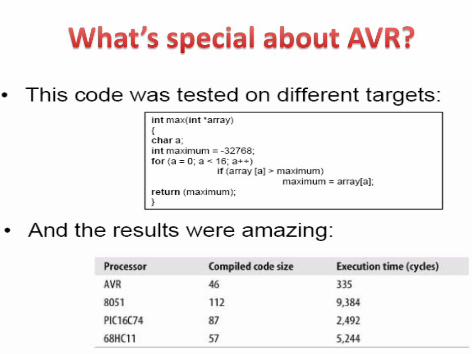
comparison between the three most commonly used families of microcontrollers:

• 8-bit microcontroller

• AVR follows Harvard Architecture
the processor is equipped with separate memories and buses for Program and the Data information. Here while an instruction is being executed, the next instruction is pre-fetched from the program memory.

• The AVR microcontrollers are based on the advanced RISC architecture and consist of 32 x 8-bit general purpose working registers.
• Within one single clock cycle, AVR can take inputs from two general purpose registers and put them to ALU for carrying out the requested operation.
• AVR does not have any register like accumulator as in 8051 family of microcontrollers.
• the operations can be performed between any of the registers and can be stored in either of them

Naming Convention

There are two flavors for Atmega16 microcontroller:
1. Atmega16:- Operating frequency range is 0 – 16 MHz.
2. Atmega16L:- Operating frequency range is 0 – 8 MHz.
If we are using a crystal of 8 MHz = 8 x 10⁶ Hertz = 8
Million cycles, then AVR can execute 8 million
instructions.


• I/O Ports: Atmega16 has four (PORTA, PORTB, PORTC and PORTD) 8-bit input-output ports.
• ADC Interface: Atmega16 is equipped with an 8 channel ADC with a resolution of 10-bits.
• Timers/Counters: Atmega16 consists of two 8-bit and one 16-bit timer/counter.
• Watchdog Timer: is present with internal oscillator. Watchdog timer continuously monitors and resets the controller if the code gets stuck at any execution action for more than a defined time interval.

• Internal Calibrated Oscillator:
Atmega16 is equipped with an internal oscillator for
driving its clock. By default Atmega16 is set to operate at
internal calibrated oscillator of 1 MHz.
The maximum frequency of internal oscillator is 8Mhz.
ATmega16 can be operated using an external crystal
oscillator with a maximum frequency of 16MHz.

• Interrupt: consists of 21 interrupt sources out of which four are external. The remaining are internal interrupts which support the peripherals like USART, ADC, Timers etc.
• USART: Universal Synchronous and Asynchronous Receiver and Transmitter interface is available for interfacing with external device capable of communicating serially (data transmission bit by bit).
• General Purpose Registers: Atmega16 is equipped with 32 general purpose registers which are coupled directly with the Arithmetic Logical Unit (ALU) of CPU.

• Memory: Atmega16 consist of three different memory sections:
1.Flash EEPROM: Flash EEPROM. Atmega16 is available with 16KB of in system programmable Flash EEPROM.
2. Byte Addressable EEPROM: Atmega16 has 512 bytes of EEPROM.
3. SRAM :Atmega16 is equipped with 1KB of internal SRAM. A small portion of SRAM is set aside for general purpose registers used by CPU and some for the peripheral subsystems of the microcontroller
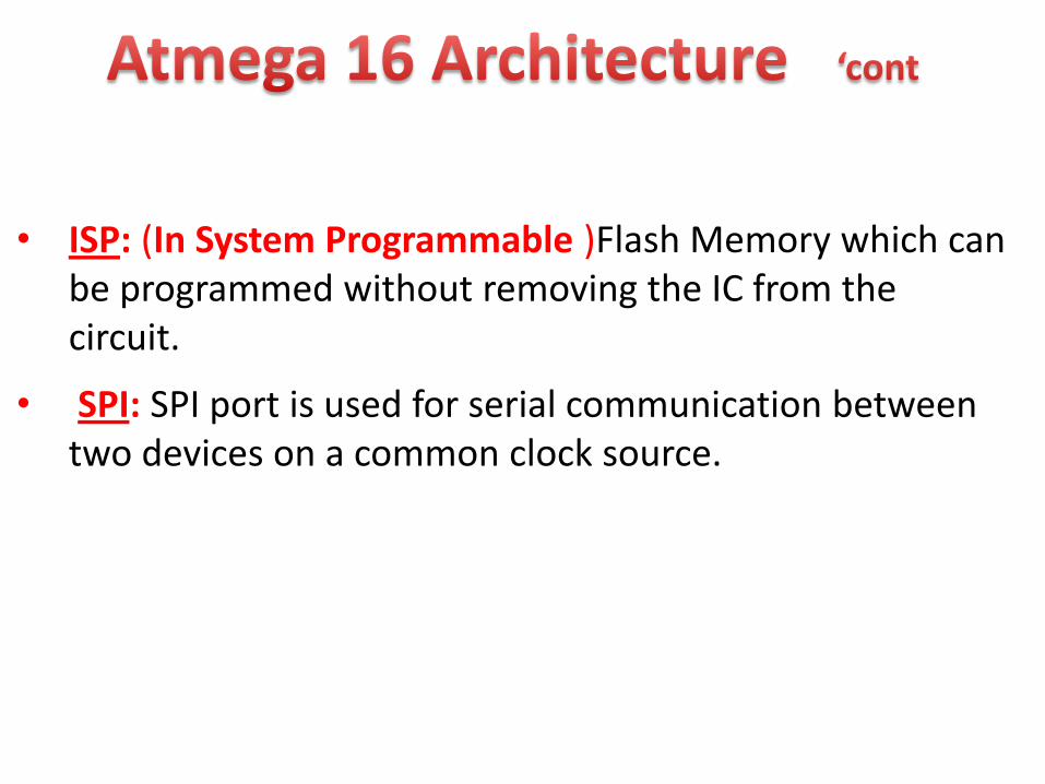
• ISP: (In System Programmable )Flash Memory which can be programmed without removing the IC from the circuit.
• SPI: SPI port is used for serial communication between two devices on a common clock source.

Download PonyProg - serial device programmer http://www.lancos.com/ppwin95.html Interfacing Schematic:

Note: Do not forget to run the setup after installing PonyProg.
Setup Information: In interface setup, select parallel and then from the drop down select AVR ISP I/O. slect the LPT Port (parallel port) available on your PC. Then click ok!
To load Hex file: Go to File-> Open Program (FLASH) file then from the drop down where ".e2p" is show, select ".hex" and load your hex file


• TWI: (Two Wire Interface )can be used to set up a network of devices, many devices can be connected over TWI interface forming a network, the devices can simultaneously transmit and receive and have their own unique address.
• DAC: Atmega16 is also equipped with a DAC interface which can be used for reverse action performed by ADC


R1: 4.7 KΩ
C1: 0.1 μF


ATmega16 have 32 Programmable I/O Lines.
• These lines are divided into 4 Ports:
– PORT A (PA7..PA0)
– PORT B (PB7..PB0)
– PORT C (PC7..PC0)
– PORT D (PD7..PD0)

• Each port consist of 3 registers:
– DDRx (Data Direction Register)
– PORTx (Output Register)
– PINx (Input Register)
• Most port pins have alternate functions in addition to
being general digital I/Os.

• Each port consist of 3 registers:
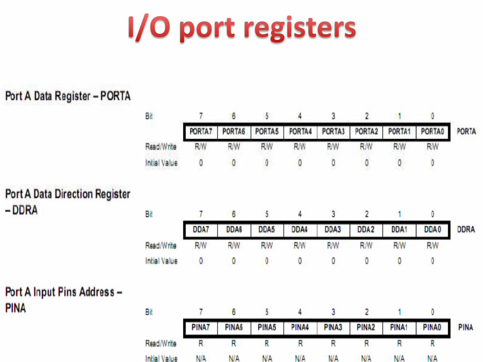

1- Decided which i/p and which output .
2-Configer the port direction use register DDRX
1 for Output.
0 for Input.
3-In Read : Use register PINx.
4-In Write : Use register PORTx.


As Output: – LEDs
– Buzzer
– Relay
– …
• As Input: – Switches
– Digital sensors
– Signal from another uC
– PC parallel port

R=10 k R=220 : 330
Pull up Resistor

Switch Debouncing

Switch Debouncing
• Could be done in software or hardware
• It relies on the fact that bouncing takes a maximum period of
20-30 ms
• The basic idea is to implement a delay after the first detected
edge, during which no scanning for the switch is done
• After the delay period is finished, scanning can proceed
• This way the bouncing can be avoided
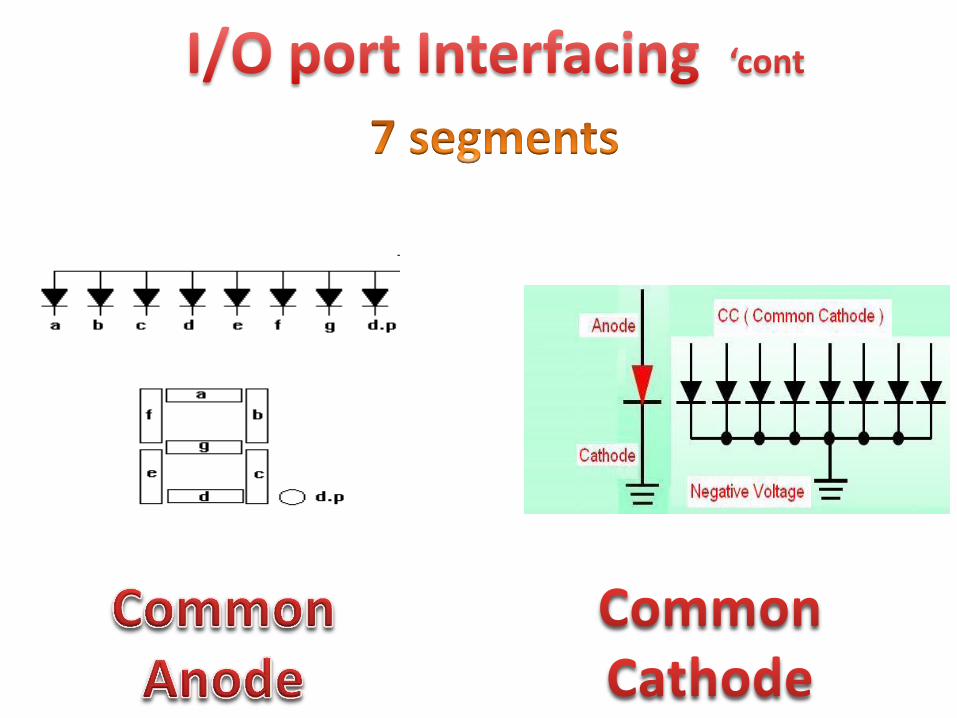
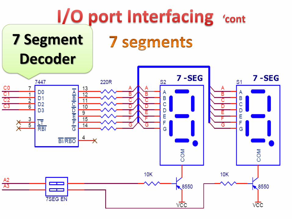
7 Segment Decoder

Two multiplexed 7seg digit with BCD decoder (7447). The decoder inputs are connected to microcontroller pins. The following table shows the required decoder input to display the numbers from 0 to 9:

Stepper motor consists of
1)Rotor: the permanent magnet that
rotates inside.
2)Stator: four coils (north, east, south,
west) that are part of the case, and which
don't move.
Rotor can be moved by sequentially
applying a pulsed DC voltage to one
or two coils at a time.
Note: Then the Number of poles of the motor
determines its step angle.

Stepper Motor Types: 1)Unipolar stepper motor The unipolar stepper motor has five or six wires and four
coils (actually two coils divided by center connections on each coil).
The center connections of the coils are tied together and used as the power connection.
They are called unipolar steppers because power always comes in on this one pole.

Stepper Motor Types: 2)Bipolar stepper motor
It has four wires coming out of it. Unlike unipolar steppers, bipolar steppers have no
common center connection. They have two independent sets of coils instead.

Unipolar stepper motor: It is most common type of stepper motor available in
the market.
A simple example of 6 lead step motor is given below
and in 5 lead step motor wire 5 and 6 are joined
together to make 1 wire as common.

The control modes
Full Stepping
Pulse Coil a1
Coil b1
Coil a2
Coil b2
1 ON
2 ON
3 ON
4 ON

Full Stepping

The control modes
Half Stepping
Pulse Coil a1 Coil b1 Coil a2 Coil b2
1 ON
2 ON ON
3 ON
4 ON ON
5 ON
6 ON ON
7 ON
8 ON ON

Half Stepping

Stepping Modes 1. Wave drive : In wave drive stepping mode only one phase is energized at a time.
2. Full Drive : In full drive, two phases are energized at a time.

Stepping Modes 3. Half Drive : In half drive, alternately one and two phases are energized. This increases the resolution of the motor.


Types of Winding and Lead-out
In unipolar step motor: there are two winding per phase. The two winding to a pole may have
one lead common i.e. center tapped.
The unipolar motor so, have five, six or eight leads.
I. Motor with six leads:
where the common of two poles are separate but center
tapped
II. Motor with five leads:
the center taps of the two poles are internally short.
III. Motor with Eight lead:
unipolar facilitates both series and parallel connection whereas
five lead and six lead motors have series connection of stator
coils.

ULN2003A Powering a Stepper
the port of AVR can only sink or source 20mA current approximately.
they cannot be used to drive the coils directly. The part that fit perfectly in this scenario is ULN2003A. It is a high voltage, high current Darlington array. It can be driven directly with a TTL level input and the
output can source up to 500ma.
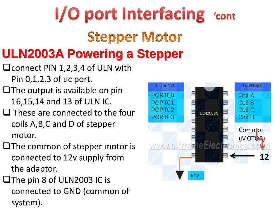
connect PIN 1,2,3,4 of ULN with Pin 0,1,2,3 of uc port.
The output is available on pin 16,15,14 and 13 of ULN IC.
These are connected to the four coils A,B,C and D of stepper motor.
The common of stepper motor is connected to 12v supply from the adaptor.
The pin 8 of ULN2003 IC is connected to GND (common of system).
12 V
Common (MOTOR)
ULN2003A Powering a Stepper

ULN2003A Powering a Stepper

BC547 Powering a Stepper
The transistors switches are used to transfer signals from the microcontroller to the stepper wires.

while(1) { stepper=0x01; delay(350); stepper=0x02; delay(350); stepper=0x04; delay(350); stepper=0x08; delay(350); }
while(1) { stepper=0x01; delay(300); stepper=0x03; delay(300); stepper=0x02; delay(300); stepper=0x06; delay(300); stepper=0x04; delay(300); stepper=0x0C; delay(300); stepper=0x08; delay(300); stepper=0x09; delay(300); }
Wave Step
Half Step

There are always two options in front of the designer whether to use
a DC motor or a stepper motor:
When it comes to speed, weight, size, cost... DC motors are always
proffered over stepper motors.
DC motor when interfaced with a microcontroller can control:
speed of motor
The direction of rotation
And encoding of the rotation made by DC motor

DC motors comes in various ratings like 6V and
12V.
It has two wires or pins.
When connected with power supply the shaft
rotates.
When reversing the polarity of input the
motor motion reverse the direction of
rotation.
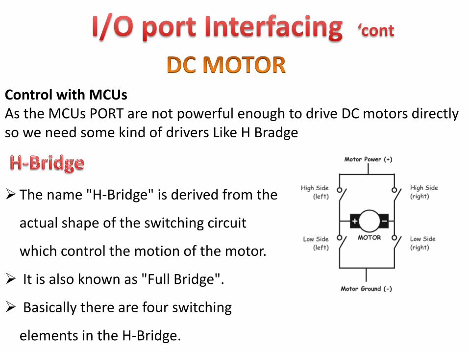
Control with MCUs As the MCUs PORT are not powerful enough to drive DC motors directly so we need some kind of drivers Like H Bradge
The name "H-Bridge" is derived from the
actual shape of the switching circuit
which control the motion of the motor.
It is also known as "Full Bridge".
Basically there are four switching
elements in the H-Bridge.

there are four switching. When these switches are turned on in pairs motor changes its
direction . if switch on High side left and Low side right then motor rotate in
forward direction. as current flows from Power supply through the motor coil goes to
ground via switch low side right.


L293D Dual DC Motor Controller
The behavior of motor for various input conditions are as follows:
B A
0 0 STOP
1 0 CW.
0 1 UCW
1 1 STOP

set appropriate levels at two PINs of the microcontroller to control the motor.
Since this chip controls two DC motors there are two more output pins (output3 and output4) and two more input pins(input3 and input4).
The INPUT3 and INPUT4 controls second motor in the same way as listed above for input A and B.
There are also two ENABLE pins they must be high(+5v) for operation, if they are pulled low(GND) motors will stop
L293D Dual DC Motor Controller

void main() { //Setup port D pin 4,5 as output. DDRD=(1<<PD4)|(1<<PD5); while(1) { //Clock wise PORTD=0B00010000; Wait(); //Anti clock wise PORTD=0B00100000; Wait(); //Stop PORTD=0; Wait(); } }
L293D Dual DC Motor Controller


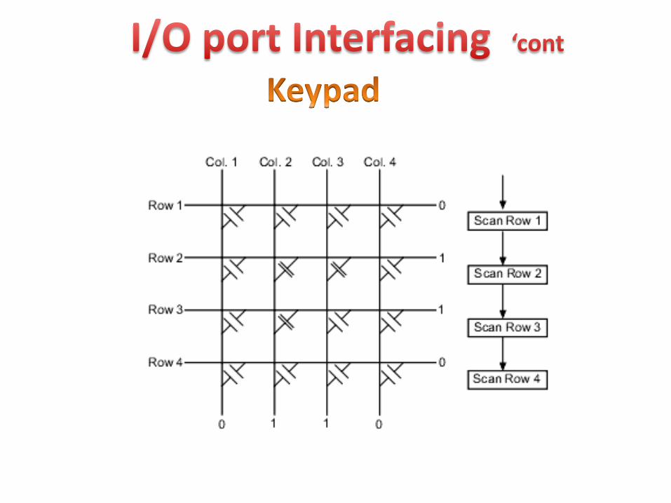
Keypads are collection of push switches arranged in the form of a matrix.
So there are rows and columns of switches.
The two connections of a switch are also connected in the matrix, so that the row has common connection and column has a common connection.

Scanning a Matrix Keypad:
To detect which key is pressed from the matrix:
1) Make row lines low one by one and read the columns.
2) first make Row1 low, then read the columns.
3) If any of the key in row1 is pressed will make the
corresponding column as low .
i.e if second key is pressed in Row1, then column2 will
give low. It mean that key 2 of Row1 is pressed.

So to scan the keypad completely:
1) make rows low one by one and read the columns.
2) If any of the button is pressed in a row, it will take the
corresponding column to a low state which tells us that a
key is pressed in that row.
3) If button 1 of a row is pressed then Column 1 will become
low, if button 2 then column2 and so on...


Pin No. Function Name
1 Ground (0V) Ground 2 Supply voltage; 5V (4.7V – 5.3V) Vcc 3 Contrast adjustment; through a variable resistor VEE
4 Selects command register when low and data register when high
Register Select
5 Low to write to the register High to read from the register
Read/write
6 Sends data to data pins when a high to low pulse is given
Enable
7
8-bit data pins
DB0 8 DB1 9 DB2
10 DB3 11 DB4 12 DB5 13 DB6 14 DB7 15 Backlight VCC (5V) Led+ 16 Backlight Ground (0V) Led-

16x2 LCD means it can display 16 characters per line and there are 2 such lines.
In this LCD each character is displayed in 5x7 pixel matrix.
LCD has two registers:
Command/Instruction Register (IR) :
stores the command instructions given to the LCD.
This instruction to LCD to do a predefined task like:
initializing, clearing the screen, setting the cursor position, controlling display etc.
Data Register (DR) :
stores the data to be displayed on the LCD.
The data is the ASCII value of the character to be displayed on the LCD.

Hex Code Command to LCD Instruction Register 1 Clear screen display 2 Return home 4 Decrement cursor 6 Increment cursor E Display ON, Cursor ON
80 Force the cursor to the beginning of the 1st line C0 Force cursor to the beginning of the 2nd line 38 Use 2 lines and 5x7 matrix
Commonly used LCD Command codes:

Programming the LCD:
Data pin8 (DB7) of the LCD is busy flag
It is read when R/W = 1 & RS = 0.
When busy flag=1
it means that LCD is not ready to accept data since it is busy with the internal operations.
before passing any data to LCD
its command register should be read and busy flag should be checked.

In this project LCD is working in 8-bit mode .
the data transferred to the LCD must be in 8-bit data form.
The PortA of ATmega16 is connected to data pins of LCD and is defined as LCD_DATA.
PortB is defined as control pins (Rs, R/W and En).
Conceptually, interfacing LCD with AVR microcontroller is similar to that of interfacing it
with any other microcontroller.
The following steps explain how LCD can be interfaced with ATMEGA 16:

To initialize LCD:
· 0x38 to initialize LCD in 8-bit mode
· 0x01 to clear LCD
· 0x0E to make cursor ON
· 0x80 to go to first line and 0th position in LCD
Delay of around 50 micro second between two commands for execution of instructions
void init_LCD(void) {
LCD_cmd(0x38); // initialization of 16X2 LCD in 8bit mode _delay_ms(1); LCD_cmd(0x01); // clear LCD _delay_ms(1); LCD_cmd(0x0E); // cursor ON _delay_ms(1); LCD_cmd(0x80); // ---8 go to first line and --0 is for 0th position delay_ms(1);
}

To send any command to LCD:
· Transfer the command to LCD_DATA port
· Set RS and RW bit to go LOW and enable as HIGH
· Give a small delay
· Set enable to LOW
void LCD_cmd(unsigned char cmd) {
LCD_DATA=cmd; ctrl =(0<<rs)|(0<<rw)|(1<<en); // RS and RW as LOW and EN as HIGH _delay_ms(1); ctrl =(0<<rs)|(0<<rw)|(0<<en); // RS, RW , LOW and EN as LOW _delay_ms(50);
}

To display any data on LCD
· Transfer the data (Ascii value of the character to be sent) to LCD_DATA port.
· Make RW as LOW and set RS and enable as HIGH.
· Give a small delay.
· Make enable pin LOW
void LCD_write(unsigned char data) {
LCD_DATA= data; ctrl = (1<<rs)|(0<<rw)|(1<<en); // RW as LOW and RS, EN as HIGH _delay_ms(1); ctrl = (1<<rs)|(0<<rw)|(0<<en); // EN and RW as LOW and RS HIGH _delay_ms(50); // delay to get things executed
}


• Flash vs E2PROM
Flash E2PROM
Programming time Faster -10 m sec Slower-25msec
E/W cycles lower-50000 Higher-1,000,000
Sector size(erasable unit of memory)
512 byte 2-4 byte
Cost Cheaper Expensive
HOW TO WRITE E2PROM DRIVER? RMW (Read Modify Write) Technique

NVRAM (Non-Volatile RAM)

Memory Mapping
16 bit processor (HCS12) CISC (von numan ) data path: 16 bit Address path :16 bit
2^16 byte(64 byte) • big problem • it is a limited address space and Mu have more
memory than what this address space covers.
32 bit processor data path: 32 bit Address path : 32 bit
2^32byte(4 GB) • no problem

Memory Mapping Control
EEPROM
RAM
FLASH

MMC
Example


• Exception handlings: – Reset. – Software Interrupts.
• Non maskable Interrupts: – doesn’t depend on global interrupt enable in processor
status word . – Usually it’s external interrupt.
• Maskable Interrupts: – Depends on global interrupt enable in processor status
word. – May be :
• External interrupt from external pin . • Internal interrupt from peripheral .
Interrupt Types:

Interrupts Concept

What happens when an interrupt occurs?
– The current instruction finishes execution.
– The address of the next instruction is calculated and pushed
onto the stack.
– All the CPU registers are pushed onto the stack.
– The program counter is loaded with the address pointed to
by the interrupt vector and execution continues.

Global Interrupt :

• In AVR processors on the other hand, interrupts are vectored, with a fixed priority scheme.
• Each interrupt has an enable bit to enable/disable the interrupt.

Interrupt vector table
• Constant table in ROM
• Special addresses with respect to CPU
• Each interrupt has specific address in interrupt vector table
• This specific address should be programmed to have the address of ISR of this interrupt
• At interrupt processing PC will contain this address or it will be an instruction to jump to this address

ATmega32 Interrupt Vector

Interrupt priorities
• Each interrupt has default priority by its location in interrupt vector table
• Some controllers provide more intelligent interrupt controller which give interrupt priority level for each interrupt
• If two interrupts have a same priority level then the rule to return to the default priority
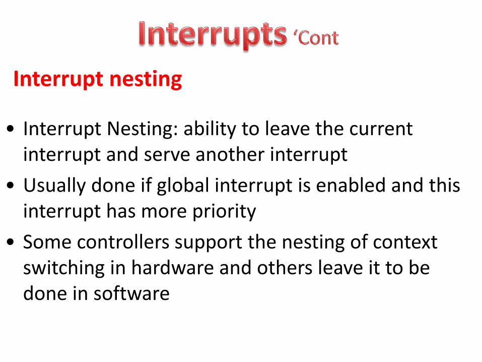
Interrupt nesting
• Interrupt Nesting: ability to leave the current interrupt and serve another interrupt
• Usually done if global interrupt is enabled and this interrupt has more priority
• Some controllers support the nesting of context switching in hardware and others leave it to be done in software

Nested Interrupt Priorities

Critical section(CS)
part of code all interrupt are disabled in it as in the case of ECU initiation

• The status register contains: – Six bits status indicators ( Z,C,H,V,N,S ) – One bit for global interrupt enable ( I )
• The status bits reflect the results of CPU operation as it executes instructions
Status Register (SREG)
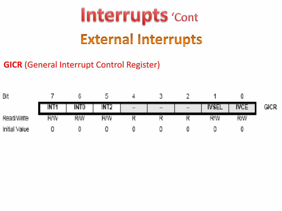
GICR (General Interrupt Control Register)

MCUCR (MCU Control Register)

MCUCSR (MCU Control and Status Register)

GIFR (General Interrupt Flag Register)

• Clear global interrupt enable: (prevent)
• Set global interrupt enable: (Allow)
• ISR

#include<avr/interrupt.h> ISR(ADC_vect) { } sei(); cli();


Serial Communication: is the process of sending data one bit at a time, sequentially, over a communication channel or computer bus.
Parallel Communication: where several bits are sent as a whole, on a link with several parallel channels.

serial connection requires fewer interconnecting
cables and hence occupies less space.
the cost of cable and synchronization difficulties
make parallel communication impractical.

• For serial communications to be accomplished there must be a transmitter (TX), and a receiver (RX).
• The TX is responsible for taking a byte (or several bits of data) in parallel, and convert them to a series of successive bits.
• The RX on the other side, collects the successive bits to reform the data once again.
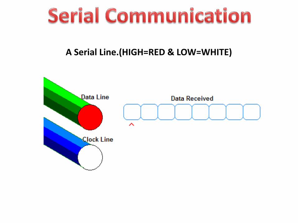
A Serial Line.(HIGH=RED & LOW=WHITE)

1-Simplex: one way communication where all signals can flow in only one direction. Example Radio & TX.
2- half-duplex system It provides for communication in both directions, but only one direction at a time (not simultaneously). Example walkie-talkie.
3-Full-duplex allows communication in both directions. Example Telephone.
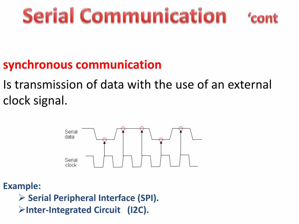
synchronous communication
Is transmission of data with the use of an external clock signal. Example:
Serial Peripheral Interface (SPI). Inter-Integrated Circuit (I2C).

Asynchronous communication
Is transmission of data without the use of an external clock signal.
Example:
Universal asynchronous receiver/transmitter (UART).
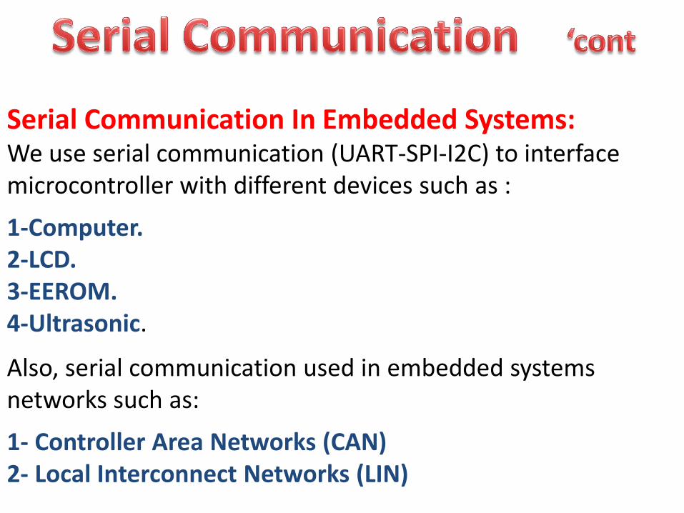
Serial Communication In Embedded Systems: We use serial communication (UART-SPI-I2C) to interface microcontroller with different devices such as :
1-Computer. 2-LCD. 3-EEROM. 4-Ultrasonic.
Also, serial communication used in embedded systems networks such as:
1- Controller Area Networks (CAN) 2- Local Interconnect Networks (LIN)

• Bit time:
– The time taken to transmit a bit/sec.
• Bit rate:
– The number of bits transmitted per second.
– Bit rate = 1 / Bit time.
• Baud Rate:
– The number of symbols signaled in a second.
– Baud rate = 1 symbol / sec.
• Symbol = bit or byte or number of bits or bytes

• When using a device has a set of 8 different symbols.
• Each symbol represents 3 bits of useful data.
• If it transmits 300 bits per second, it gathers each 3 bits in 1 symbol.
• So it transmits 100 symbol per second
– 300 bit per second (bit rate)
– 100 baud (baud rate)


It also called Serial Communication Interface(SCI)
full-duplex communication.
Asynchronous communication.
Compatible with PC .
The Standard bit rates are:
100, 200, 300, 1200, 2400, 4800, 9600, 19200,
38400, 57600, 115200 bps.


• Frame : A frame is the unit of transmission in serial communications.
• A frame contains: – Start bit: To declare the start of transmission.
– Data bits: 4,5,6,7, or 8 bits of useful data bits.
– Parity bit : To check for transmission errors.
– Stop bit: To declare end of frame.
• Parity bit is used to check the integrity of a frame and signal if an error occurred during transmission.

• Parity : – Parity bit is an extra bit added to the end of a
frame.
• Even parity : – The number of ‘1’ symbols inside a frame must
always be even.
• Odd parity : – The number of ‘1’ symbols inside a frame must
always be odd.
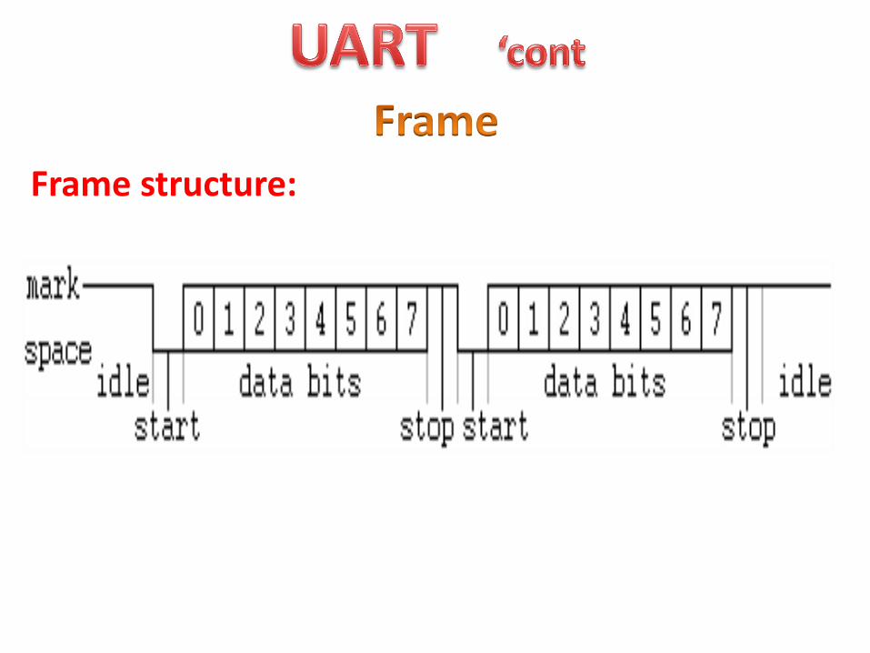
Frame structure:

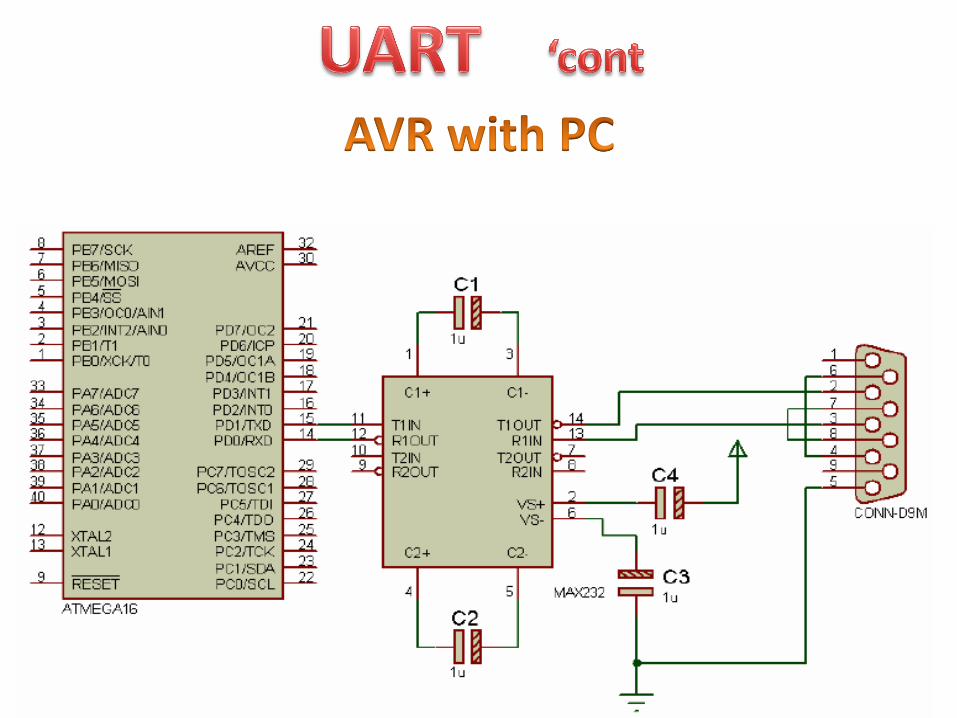
RS232 Data Interface PC serial interface.
SPACE (0) will be between +3 to +15 volts.
MARK (1) will be between -3 and -15 volts.

Microcontroller O/P voltages: o0 v for logic 0. o5v for logic 1.
MAX232
Is an IC that converts signals from an RS-232 serial port to signals suitable for use in TTL compatible digital logic circuits

Hyper Terminal from Start > Programs > Accessories > Communications

Bit No 7 6 5 4 3 2 1 0
Name RXC TXC UDRE FE DOR PE U2X MPCM
UCSRA: USART Control and Status Register A
RXC this bit is set when the USART has completed receiving a byte from the host UDRE this bit set when UDR emty.
Bit No 7 6 5 4 3 2 1 0
Name RXCIE TXCIE UDRIE RXEN TXEN UCSZ2 RXB8 TXB8
UCSRB: USART Control and Status Register B
RXCIE: Receive Complete Interrupt Enable TXCIE: Transmit Complete Interrupt Enable RXEN: Receiver Enable TXEN: Transmitter Enable UCSZ2: USART Character Size

Bit No 7 6 5 4 3 2 1 0
Name URSEL UMSEL UPM1 UPM0 USBS UCSZ1 UCSZ0
URSEL: USART register select. The UCSRC and the UBRRH register shares same address so to determine which register user want to write is decided with the 7th(last) bit of data if its 1 then the data is written to UCSRC else it goes to UBRRH. USART Mode Select
UMSEL Mode
0 Asynchronous
1 Synchronous
USBS Stop Bit(s)
0 1 BIT
1 2 BIT
UCSZ2 UCSZ1 UCSZ0 Character Size
0 0 0 5Bit
0 0 1 6Bit
0 1 0 7Bit
0 1 1 8Bit
1 0 0 Reserved
1 0 1 Reserved
1 1 0 Reserved
1 1 1 9Bit
UCSRC: USART Control And Status Register C
USBS: USART Stop Bit Select

UDR: Data Register UBRR: USART Baud Rate Register:

void MCL_UART_Init(void)
void MCL_UART_SendByte(unsigned char byte)
void MCL_UART_StartSendArray(unsigned char length, unsigned char * array)
void MCL_UART_StartReceving(void)
void MCL_UART_GetReceivedData(unsigned char length, unsigned char * arr_rx)
int Compare (unsigned char * arr_rx,unsigned char length)
//equal=1 //not equal=0


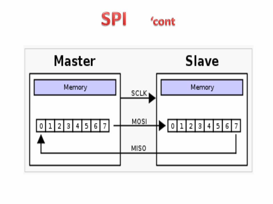
• SPI is a Synchronous Serial Communication.
• SPI is a Master/Slave Communication.
• SPI have only 1 Master and multi-Slaves.
• Totally Full-Duplex communication.
• Cascade Slave Communication.


• SPI are not supported by PC directly.
• It need either software emulation through a legacy
port, or a special hardware.


It also called two wire interface (TWI)
Multi-Master Bus.
7 bit address space Maximum 112 nodes(16 reserved).
Normal Mode 100 Kb/s (The most common).
Fast Mode 400 kb/s.
High-Speed Mode 3.4 Mb/s.
Clock Stretching.


• Types of Messages:
– “Single” message
• where a master reads/writes data to a slave.
– “Combined” messages
• where a master issues at least two reads and/or writes to one or more slaves.
In a combined message, each read or write begins with a START and the slave address. After the first START, these are also called "repeated START" bits; repeated START bits are not preceded by STOP bits, which is how slaves know the next transfer is part of the same message.

Start Bit
ACk
7 Bit Address
Read or Write
Send or Receive
Stop
If Combined MSG

1) The master is initially in master transmit mode by sending a
start bit.
2) Master send the 7-bit address of the slave it wishes to
communicate with. (0 Dominant )
3) Master send single bit representing whether it wishes to
write(0) to or read(1) from the slave.

4)If the slave exists on the bus then it will respond
with an ACK bit (active low for acknowledged) for that
address.
5)The master then continues in either transmit or
receive mode and the slave continues in its
complementary mode .

• The address and the data bytes are sent most
significant bit first. The start bit is indicated by a
high-to-low transition of SDA with SCL high; the stop
bit is indicated by a low-to-high transition of SDA
with SCL high.

• If the master wishes to write to the slave then it
repeatedly sends a byte with the slave sending an
ACK bit. (In this situation, the master is in master
transmit mode and the slave is in slave receive
mode).

• If the master wishes to read from the slave then it
repeatedly receives a byte from the slave, the
master sending an ACK bit after every byte but the
last one. (In this situation, the master is in master
receive mode and the slave is in slave transmit
mode).

6) The master then ends transmission with a stop
bit, or it may send another START bit if it wishes to
retain control of the bus for another transfer (a
"combined message").


Every master monitors the bus for start and stop bits, and does not start a message while another master is keeping the bus busy.
However, two masters may start transmission at about the same time; in this case, arbitration occurs.
Slave transmit mode can also be arbitrated, when a master addresses multiple slaves, but this is less common.


• I2C are not supported by PC directly.
• It need either software emulation through a legacy
port, or a special hardware.

Touchscreens.
Flash,MMC,SD,EEPROM memories.
LCD Displays.
DSP’s,FPGA’s.

The timer of the AVR can be monitor three Events through State register (TIMSK):
Timer Overflow.
Compare Match.
Input Capture.
Also, Timer use in PWM Generation.

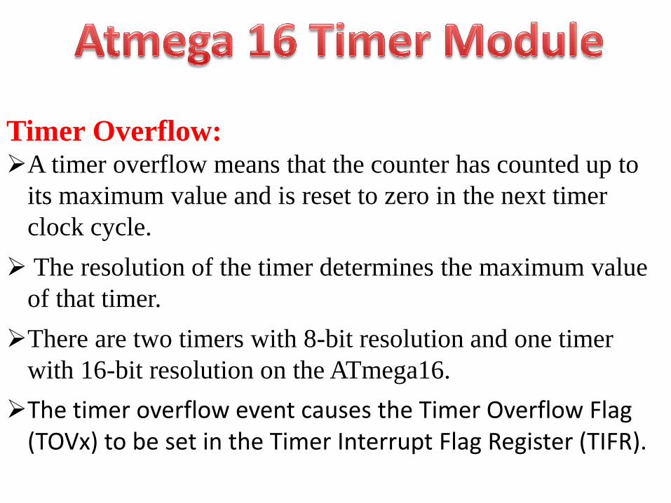
Timer Overflow: A timer overflow means that the counter has counted up to
its maximum value and is reset to zero in the next timer
clock cycle.
The resolution of the timer determines the maximum value
of that timer.
There are two timers with 8-bit resolution and one timer
with 16-bit resolution on the ATmega16.
The timer overflow event causes the Timer Overflow Flag (TOVx) to be set in the Timer Interrupt Flag Register (TIFR).

Compare Match In cases where it is not sufficient to monitor a timer
overflow. the compare match interrupt can be used. The Output Compare Register (OCRx) can be loaded with
a value [0.. MaxVal] which the timer will be checked against every timer cycle.
When the timer reaches the compare value, the corresponding Output Compare Flag (OCFx) in the TIFR register is set.
The Timer can be configured to clear the count register to “0” on a compare match.

Compare Match
Related output pins can be configured to be set, cleared or toggled automatically on a compare match.

Input Capture
The AVR has an input pin to trigger the input capture event.
A signal change at this pin causes the timer value to be read and saved in the Input Capture Register (ICRx).
At the same time the Input Capture Flag (ICFx) in the TIFR will be set.
This is useful to measure the width of external pulses.
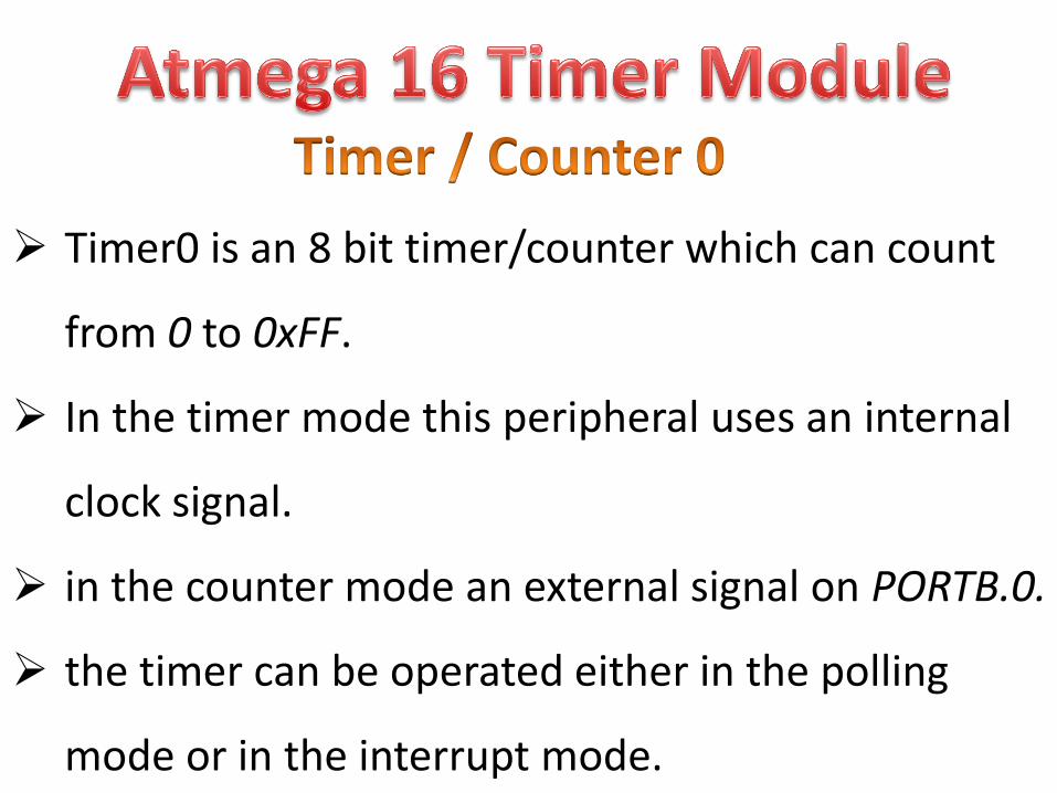
Timer0 is an 8 bit timer/counter which can count
from 0 to 0xFF.
In the timer mode this peripheral uses an internal
clock signal.
in the counter mode an external signal on PORTB.0.
the timer can be operated either in the polling
mode or in the interrupt mode.

Used registers: • Timer registers: TCCR0 (Timer/Counter 0 Control Register) TCNT0 (Timer/Counter 0 Value)
• Interrupt registers: TIFR (Timer Interrupt Flag Register) TIMSK (Timer Interrupt Mask Register) SREG (I bit - General Interrupt Enable)

TCCR0 (Timer/Counter 0 Control Register)
Define module ON/OFF Define module T/C
Prescaler

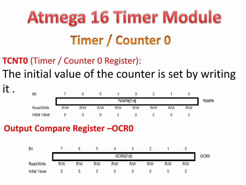
TCNT0 (Timer / Counter 0 Register):
The initial value of the counter is set by writing it .
Output Compare Register –OCR0

TIMSK (Timer / Counter Interrupt Mask)
TOIE0: Timer Overflow Interrupt Enable OCIE0: Output Compare Match Interrupt Enable

TIFR (Timer / Counter Interrupt Flag Register)
TOV0: Timer/Counter0 Overflow Flag OCF0: Output Compare Flag 0

Initializations example : // Timer/Counter 0 initialization with clock = oscillator / 1024 // Timer initial value is 0xf0; TCCR0=0x05; TCNT0=0xf0; // Timer/Counter 0 initialization // Clock source: T0 pin Rising Edge TCCR0=0x07;

TCCR0 (Timer/Counter 0 Control Register)
Wave Generation Mode

Compare Output Mode, non-PWM Mode

Clear Timer on Compare Match (CTC) Mode (WGM01:0 = 2): the OCR0 Register is used to manipulate the counter resolution. In CTC mode the counter is cleared to zero when the counter value (TCNT0) matches the OCR0.
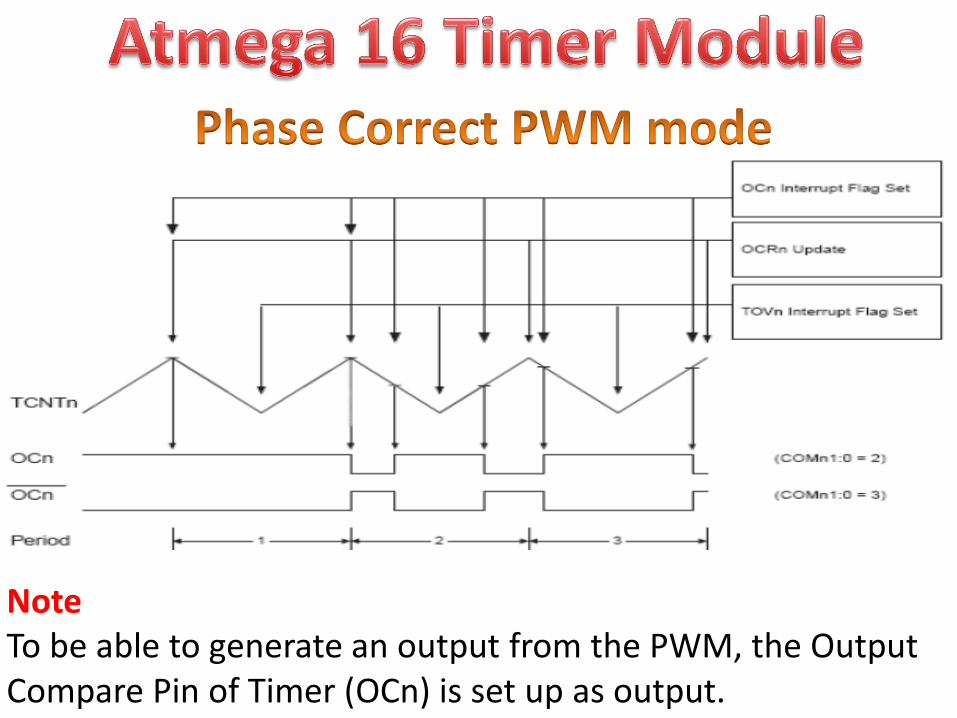
Note To be able to generate an output from the PWM, the Output Compare Pin of Timer (OCn) is set up as output.

Compare Output Mode, non-PWM Mode
note that the Data Direction Register (DDR) bit corresponding to the OC0 pin must be set in order to enable the output driver.

The PWM is used to generate a pulse train with varying duty-cycle.
An analog filter can be used to shape the digital PWM output to obtain an analog signal such as a sine wave.
In the AVR, the timer/counters are used to generate PWM signals.
To change the PWM base frequency, the timer clock frequency and top counter value is changed. Faster clock and/or lower top value will increase the PWM base frequency, or timer overflow frequency.
With full resolution (top value 255) the maximum PWM base frequency is 250 kHz.

Altering the value of the Output Compare Registers (OCR) changes the duty cycle. Increasing the OCR value increases the duty cycle.

The fast Pulse Width Modulation or fast PWM mode
(WGM01:0 = 3) provides a high frequency.
PWM waveform generation option.
The fast PWM differs from the other PWM option by its
single-slope operation.
The counter counts from BOTTOM to MAX then restarts
from BOTTOM.
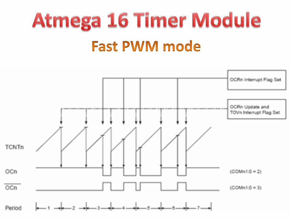

In fast PWM mode, the compare unit allows generation of
PWM waveforms on the OC0 pin.
Setting the COM01:0 bits to 2 will produce a non-inverted
PWM .
Inverted PWM output can be generated by setting the
COM01:0 to 3.
Compare Output Mode, Fast PWM Mode:

The phase correct PWM mode (WGM01:0 = 1) provides a high resolution phase correct PWM
waveform generation option. The phase correct PWM mode is based on a
dual slope operation. The counter counts repeatedly from
BOTTOM to MAX and then from MAX to BOTTOM.
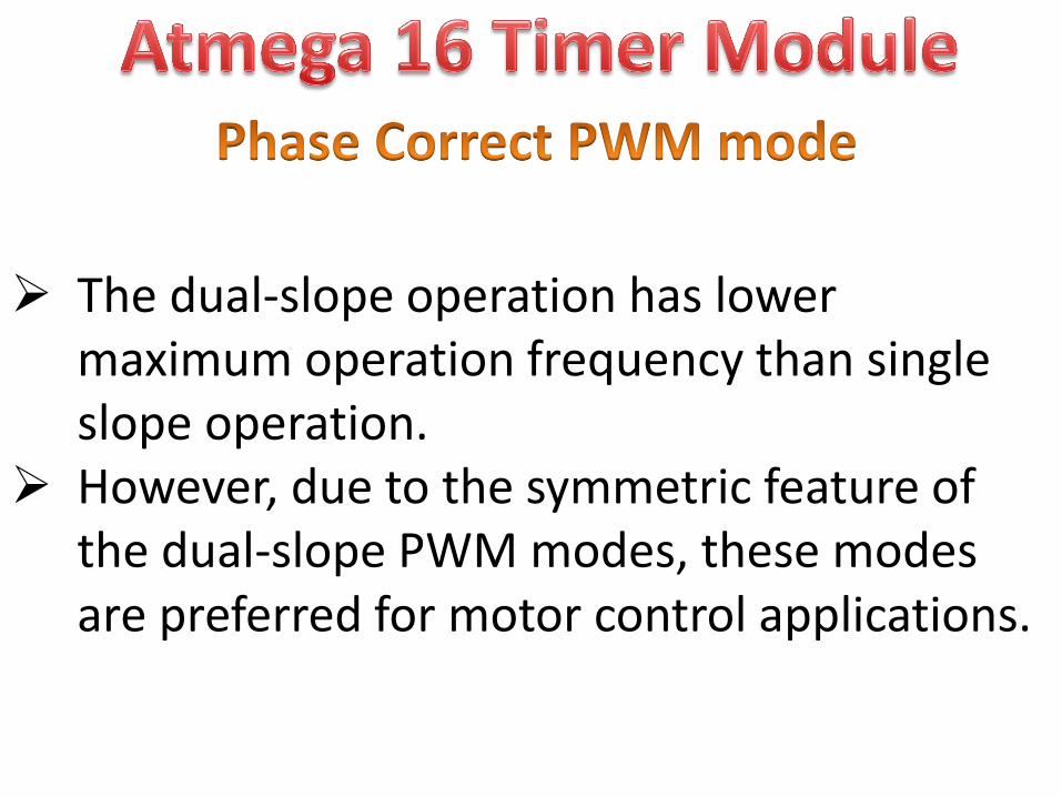
The dual-slope operation has lower maximum operation frequency than single slope operation.
However, due to the symmetric feature of the dual-slope PWM modes, these modes are preferred for motor control applications.

The PWM resolution for the phase correct PWM mode is fixed to eight bits.
In phase correct PWM mode the counter is incremented until the counter value matches MAX. When the counter reaches MAX, it changes the count direction.
The TCNT0 value will be equal to MAX for one timer clock cycle
Note To be able to generate an output from the PWM, the Output Compare Pin of Timer (OCn) is set up as output.

Initializations example : // Timer/Counter 0 initialization // Clock source: System Clock / 1024 // Mode: Non-Inverted Fast PWM TCCR0=0x6D; TCNT0=0x00; OCR0=0x00; TIMSK=0x02; OCR0 = x; // x is a variable which change the duty cycle.

The ADC is enabled by setting the ADC Enable bit,
ADEN in ADCSRA.
Voltage reference and input channel selections will
not go into effect until ADEN is set.
The ADC does not consume power when ADEN is
cleared,
so it is recommended to switch off the ADC before
entering power saving sleep modes.

The ADC generates a 10-bit result which is
presented in the ADC Data Registers, ADCH and
ADCL.
By default, the result is presented right adjusted,
But can optionally be presented left adjusted by
setting the ADLAR bit in ADMUX.

If the result is left adjusted and no more than 8-bit
precision is required, it is sufficient to read ADCH.
Otherwise, ADCL must be read first, then ADCH, to
ensure that the content of the Data Registers
belongs to the same conversion.

ADMUX (ADC Multiplexer Selection Register)

ADLAR: ADC Left Adjust Result MUX4:0: Analog Channel Selection Bits:
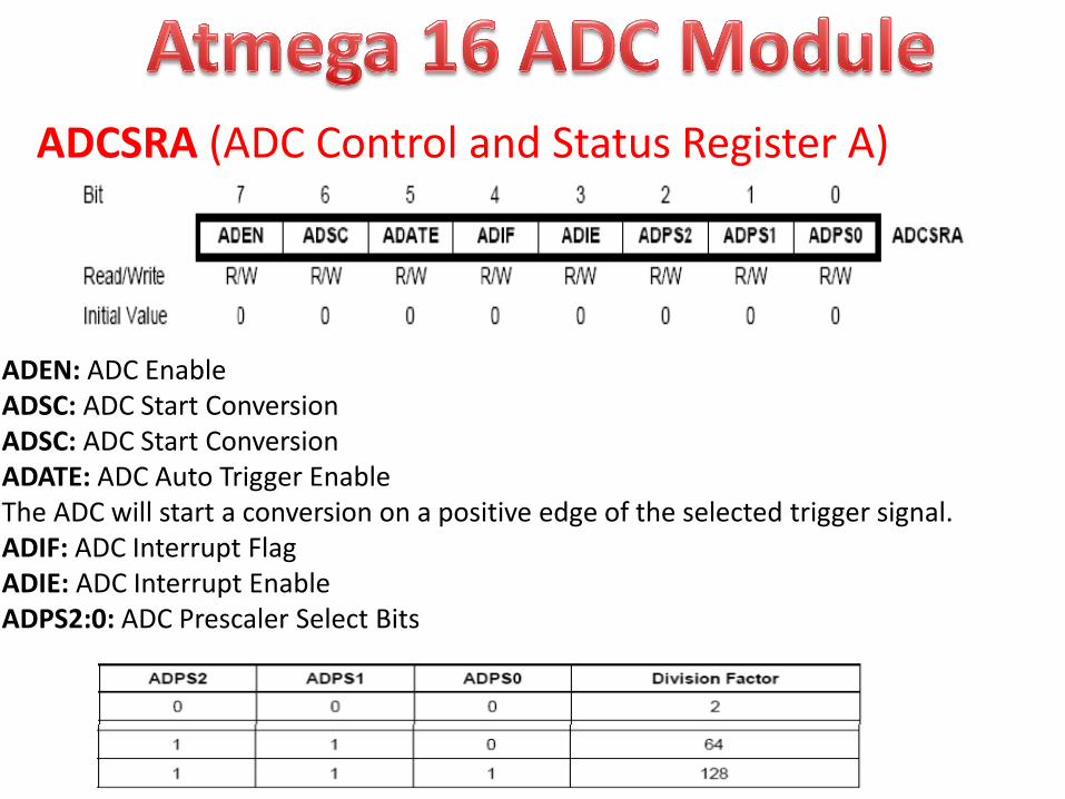
ADCSRA (ADC Control and Status Register A)
ADEN: ADC Enable ADSC: ADC Start Conversion ADSC: ADC Start Conversion ADATE: ADC Auto Trigger Enable The ADC will start a conversion on a positive edge of the selected trigger signal. ADIF: ADC Interrupt Flag ADIE: ADC Interrupt Enable ADPS2:0: ADC Prescaler Select Bits

ADCL and ADCH (The ADC Data Register)

SFIOR (Special Function IO Register)

Example: ADMUX=0x60; // ADC Reference Volt: AVCC pin, ADLAR, ADC Clock frequency: XTAL / 2
ADCSRA=0x84; // ADC Enable, ADc Interrupt enable
// Start the AD conversion ADCSRA|=0x40;
// Wait for the AD conversion to complete while ((ADCSRA & 0x10)==0);
// clear Interrupt flag ADCSRA|=0x10;

ITI Lecture. ITI Material. AVR Microcontroller By Eng. Mohamed El Sobky http://www.8051projects.net http://www.engineersgarage.com/
You must visit it