
Interconnect Effects I/O, Power Distribution
28
1 EE141 Interconnect Effects I/O, Power Distribution EE141- Fall 2002 Lecture 25 EE141 Announcements l Homework 9 due next Tuesday l Hardware lab this week l Project phase 2 due in two weeks
Transcript of Interconnect Effects I/O, Power Distribution

1
EE141
Interconnect EffectsI/O, Power Distribution
EE141- Fall 2002Lecture 25
EE141
Announcements
l Homework 9 due next Tuesdayl Hardware lab this weekl Project phase 2 due in two weeks

2
EE141
Today’s Lecture
l Impact of interconnects» I/O» Power distribution
EE141
Interconnect Issues

3
EE141
Impact of Interconnect Parasitics
• Reduce Robustness
• Affect Performance
Classes of Parasitics
• Capacitive
• Resistive
• Inductive
EE141
INTERCONNECT
Dealing with Capacitance

4
EE141
Capacitive CrosstalkDynamic Node
VDD
PDNIn1In2In3
CLK
CY
CXYY
X
2.5 V
0 V
CLK
3 x 1 µm overlap: 0.19 V disturbance
EE141
Capacitive CrosstalkDriven Node
0 0.2 0.4 0.6 0.8 1
x 10-9
0
0.05
0.1
0.15
0.2
0.25
0.3
0.35
0.4
0.45
0.5
V (
Vol
t)
t(sec)
Y
XCXY
CY
VX
RYτXY = RY(CXY+CY)
tr
Keep time-constant smaller than rise time

5
EE141
Delay Degradation
Cc
- Impact of neighboring signal activity on switching delay
- When neighboring lines switch in opposite direction of victim line, delay increases
Miller EffectMiller Effect
- Both terminals of capacitor are switched in opposite directions(0 → Vdd, Vdd → 0)
- Effective voltage is doubled and additional charge is needed (from Q=CV)
EE141
Interconnect ProjectionsLow-k dielectrics
l Both delay and power are reduced by dropping interconnect capacitance
l Types of low-k materials include: inorganic (SiO2), organic (Polyimides) and aerogels (ultra low-k)
l The numbers below are on the conservative side of the NRTS roadmap
Generation 0.25µm
0.18µm
0.13µm
0.1µm
0.07µm
0.05µm
DielectricConstant
3.3 2.7 2.3 2.0 1.8 1.5
ε

6
EE141
How to Battle CapacitiveCrosstalk
Substrate (GND)
GND
ShieldinglayerVDD
GND
Shieldingwire
l Avoid large crosstalk cap’sl Avoid floating nodesl Isolate sensitive nodesl Control rise/fall timesl Shield!l Differential signalling
EE141
Driving Large Capacitances
VDD
Vin Vout
CL
tpHL = CL Vswing/2
Iav
TransistorSizing

7
EE141
Using Cascaded Buffers
CL = 20 pF
In Out
1 2 N
0.25 µm processCin = 2.5 fFtp0 = 30 ps
F = CL/Cin = 8000fopt = 3.6 N = 7tp = 0.76 ns
EE141
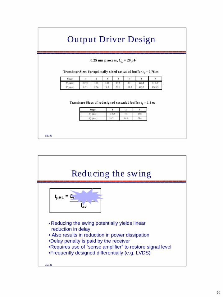
Output Driver Design
l Trade off Performance for Area and Energy» Given tpmax find N and f
l Area
l Energy
( ) minminmin12
11
11
...1 AfF
Af
fAfffA
NN
driver −−
=−−
=++++= −
( ) 22212
111
...1 DDL
DDiDDiN
driver VfC
VCfF
VCfffE−
≈−−
=++++= −
8
EE141
Output Driver Design
Transistor Sizes for optimally-sized cascaded buffer tp = 0.76 ns
Transistor Sizes of redesigned cascaded buffer tp = 1.8 ns
0.25 µm process, CL = 20 pF
EE141
Reducing the swing
tpHL = CL Vswing/2
Iav
• Reducing the swing potentially yields linear reduction in delay
• Also results in reduction in power dissipation•Delay penalty is paid by the receiver •Requires use of “sense amplifier” to restore signal level•Frequently designed differentially (e.g. LVDS)
9
EE141
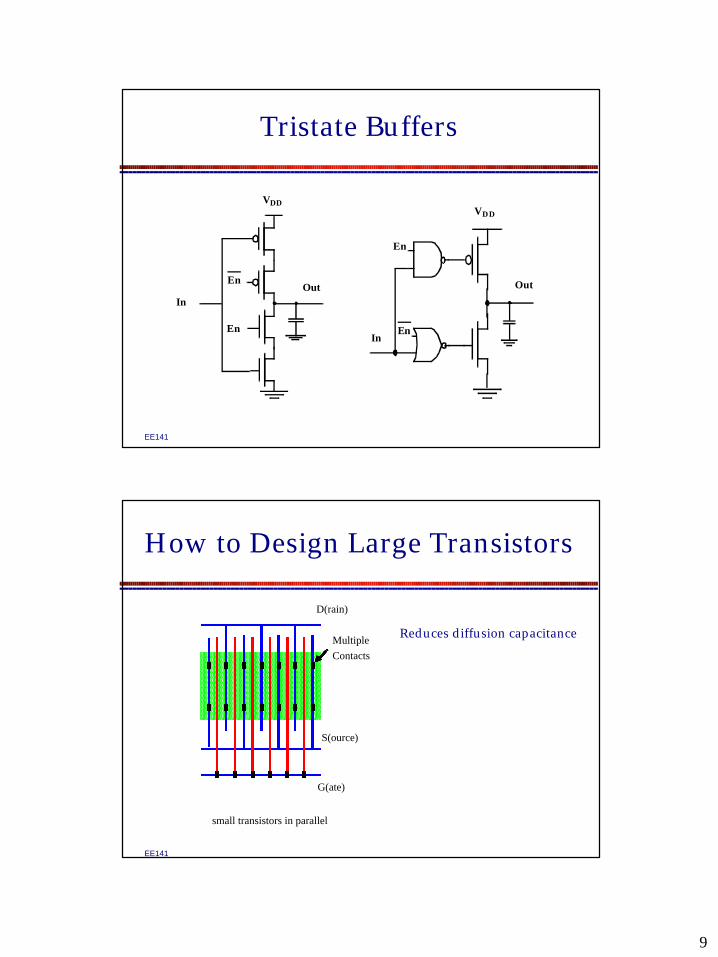
Tristate Buffers
In
VDD
En
EnOut
VDD
Out
In
En
En
EE141
How to Design Large Transistors
G(ate)
S(ource)
D(rain)
MultipleContacts
small transistors in parallel
Reduces diffusion capacitance

10
EE141
Bonding Pad Design
Bonding Pad
Out
InVDD GND
100 µm
GND
Out
EE141
ESD Protection
Diode
PAD
VDD
R D1
D2
X
C

11
EE141
ESD Protection
l When a chip is connected to a board, there is unknown (potentially large) static voltage difference
l Equalizing potentials requires (large) charge flow through the pads
l Diodes sink this charge into the substrate –need guard rings to pick it up.
EE141
Chip Packaging
ChipL
L´
Bonding wire
Mountingcavity
Leadframe
Pin
•Bond wires (~25µm) are used to connect the package to the chip
• Pads are arranged in a frame around the chip
• Pads are relatively large (~100µm in 0.25µm technology),with large pitch (100µm)
•Many chips areas are ‘pad limited’

12
EE141
Pad Frame
Layout Die Photo
EE141
Chip Packaging
l An alternative is ‘flip-chip’:» Pads are distributed around the chip» The soldering balls are placed on pads» The chip is ‘flipped’ onto the package» Can have many more pads

13
EE141
INTERCONNECT
Dealing with Resistance
EE141
Impact of Resistance
l We have already learned how to drive RC interconnect
l Impact of resistance is commonly seen in power supply distribution:» IR drop» Voltage variations
l Power supply is distributed to minimize the IR drop and the change in current due to switching of gates

14
EE141
RI Introduced Noise
VDD
X
I
I
R’
R
VDD - ∆V’
∆V
∆V
φpre
EE141
Power and Ground Distribution
GND
VDD
Logic
GND
VDD
Logic
GND
VDD
(a) Finger-shaped network (b) Network with multiple supply pins

15
EE141
Resistance and the Power Distribution Problem
Source: Simplex
•• Requires fast and accurate peak current predictionRequires fast and accurate peak current prediction•• Heavily influenced by packaging technologyHeavily influenced by packaging technology
BeforeBefore AfterAfter
EE141
Power Distribution
l Low-level distribution is in Metal 1l Power has to be ‘strapped’ in higher layers of
metal.l The spacing is set by IR drop,
electromigration, inductive effectsl Always use multiple contacts on straps
16
EE141
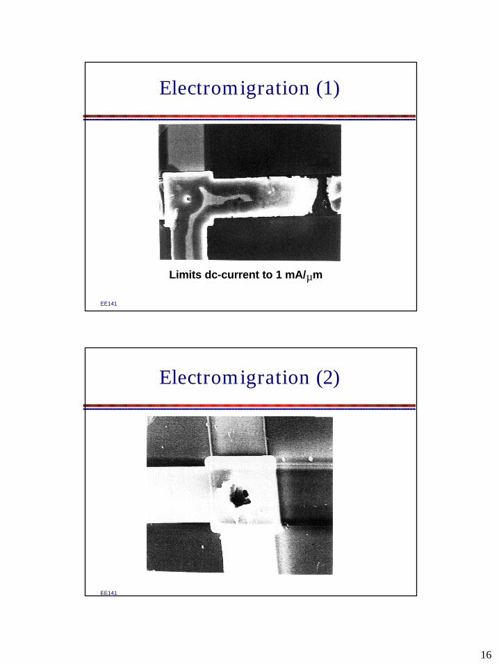
Electromigration (1)
Limits dc-current to 1 mA/µm
EE141
Electromigration (2)

17
EE141
The Impact of Resistivity
CN-1 CNC2
R1 R2
C1
Tr
Vin
RN-1 RN
0 0.5 1 1.5 2 2.5 3 3.5 4 4.5 50
0.5
1
1.5
2
2.5
time (nsec)
volt
ag
e (
V)
x= L/10
x = L/4
x = L/2
x= L
0 0.5 1 1.5 2 2.5 3 3.5 4 4.5 50
0.5
1
1.5
2
2.5
time (nsec)
volt
ag
e (
V)
x= L/10
x = L/4
x = L/2
x= L
Diffused signal Diffused signal propagationpropagation
Delay ~ LDelay ~ L22
The distributedThe distributed rcrc--lineline
EE141
The Global Wire Problem( )outwwdoutdwwd CRCRCR693.0CR377.0T +++=
Challengesl No further improvements to be expected after the
introduction of Copper (superconducting, optical?)l Design solutions
» Use of fat wires» Insert repeaters — but might become prohibitive (power, area)» Efficient chip floorplanning
l Towards “communication-based” design » How to deal with latency?» Is synchronicity an absolute necessity?
18
EE141
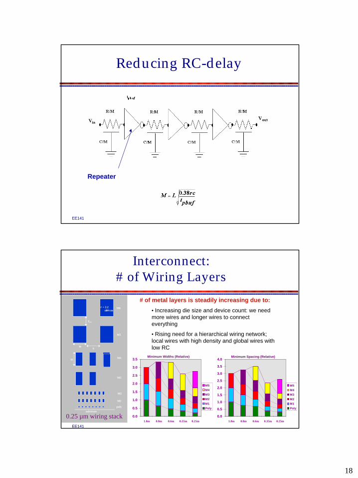
Reducing RC-delay
Repeater
EE141
Interconnect:# of Wiring Layers
# of metal layers is steadily increasing due to:
• Increasing die size and device count: we need more wires and longer wires to connect everything
• Rising need for a hierarchical wiring network; local wires with high density and global wires with low RC
substrate
poly
M1
M2
M3
M4
M5
M6
Tins
H
WS
ρ = 2.2 µΩ-cm
0.25 µm wiring stack
Minimum Widths (Relative)
0.0
0.5
1.0
1.5
2.0
2.5
3.0
3.5
1.0µ 0.8µ 0.6µ 0.35µ 0.25µ
M5
M4
M3
M2
M1
Poly
Minimum Spacing (Relative)
0.0
0.5
1.0
1.5
2.0
2.5
3.0
3.5
4.0
1.0µ 0.8µ 0.6µ 0.35µ 0.25µ
M5
M4
M3
M2
M1
Poly

19
EE141
Interconnect Projections: Copper
l Copper is planned in full sub-0.25 µm process flows and large-scale designs (IBM, Motorola, IEDM97)
l With cladding and other effects, Cu ~ 2.2 µΩ-cm vs. 3.5 for Al(Cu) ⇒40% reduction in resistance
l Electromigration improvement; 100X longer lifetime (IBM, IEDM97)» Electromigration is a limiting factor
beyond 0.18 µm if Al is used (HP, IEDM95)
Vias
EE141
INTERCONNECT
Dealing with Inductance

20
EE141
Common Wire Cross-Sections
CoaxialCable
TriplateStrip Line
MicroStrip Wire aboveGround Plane
cl = εµ1
2
1
2
log2
log2
rr
rr
l
c
πµ
πε
=
=
c - capacitance/lengthl - inductance/length
=
=
Wh
l
Wh
c
µ
ε
EE141
L di/dt
CL
V’DD
VDD
L i(t)
VoutVin
GND’
L
Impact of inductance on supply voltages:• Change in current induces the change in voltage• Longer supply lines have larger L

21
EE141
L di/dt: Simulation
t
t
t
vout
iL
vL
20mA
40mA
5V
0.2V
0.0
1.02.0
3.0
4.0
5.0
Vou
t(V)
0
10
20
I L (m
A)
2 4 6 8 10t (nsec)
-0.3
-0.1
0.1
0.3
0.5
VL(V
)
tfall = 0.5 nsec
tfall = 4 nsec
Signals Waveforms for Output Driver connected To Bonding Pads(a) vout; (b) iL and (c) vL.
The Results of an Actual Simulation are Shown on the Right Side.
EE141
Choosing the Right Pin
ChipL
L´
Bonding wire
Mountingcavity
Leadframe
Pin
22
EE141
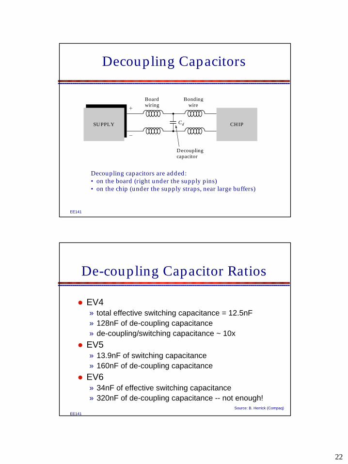
Decoupling Capacitors
SUPPLY
Boardwiring
Bondingwire
Decouplingcapacitor
CHIPCd
1
2
Decoupling capacitors are added: • on the board (right under the supply pins)• on the chip (under the supply straps, near large buffers)
EE141
De-coupling Capacitor Ratios
l EV4» total effective switching capacitance = 12.5nF» 128nF of de-coupling capacitance» de-coupling/switching capacitance ~ 10x
l EV5» 13.9nF of switching capacitance » 160nF of de-coupling capacitance
l EV6» 34nF of effective switching capacitance» 320nF of de-coupling capacitance -- not enough!
Source: B. Herrick (Compaq)
23
EE141
EV6 De-coupling CapacitanceDesign for ∆Idd= 25 A @ Vdd = 2.2 V, f = 600
MHz» 0.32-µF of on-chip de-coupling capacitance was
added– Under major busses and around major gridded clock drivers– Occupies 15-20% of die area
» 1-µF 2-cm2 Wirebond Attached Chip Capacitor (WACC) significantly increases “Near-Chip” de-coupling
– 160 Vdd/Vss bondwire pairs on the WACC minimize inductance
Source: B. Herrick (Compaq)
EE141
EV6 WACC
587 IPGA
MicroprocessorWACC
Heat Slug
389 Signal - 198 VDD/VSS Pins389 Signal Bondwires
395 VDD/VSS Bondwires
320 VDD/VSS Bondwires
Source: B. Herrick (Compaq)

24
EE141
Design Techniques to address L di/dt
l Separate power pins for I/O pads and chip corel Multiple power and ground pinsl Position of power and ground pins on packagel Increase tr and tfl Advanced packaging technologiesl Decoupling capacitances on chip and on board
EE141
The Transmission Line
Vin
r l
c
r l
c
r l
c
r l
c
Voutx
g g g g
The Wave Equation

25
EE141
Lossless Transmission Line -Parameters
vacuumspeed of light in
EE141
Wave Propagation Speed
26
EE141
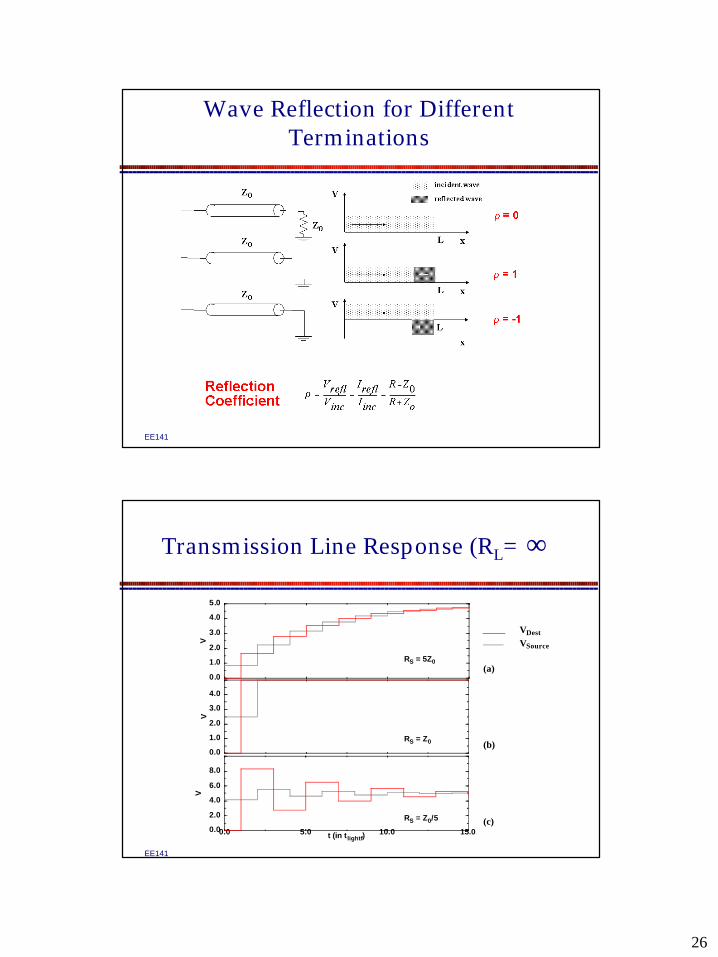
Wave Reflection for Different Terminations
EE141
Transmission Line Response (RL= ∞)
0.0
1.0
2.0
3.0
4.0
5.0
V
0.0
1.0
2.0
3.0
4.0
V
0.0 5.0 10.0 15.0t (in t lightf)0.0
2.0
4.0
6.0
8.0
V
RS = 5Z0
RS = Z0
RS = Z0/5
(a)
(b)
(c)
VDest
VSource

27
EE141
Lattice Diagram
VSource VDest
0.8333 V
1.6666 V+ 0.8333
+ 0.8333
+ 0.5556
+ 0.5556
+ 0.3704
+ 0.2469
+ 0.3704
+ 0.2469
2.2222 V
3.1482 V
3.7655 V
...
2.7778 V
3.5186 V
4.0124 V
L/ν
t
EE141
Critical Line Lengths versus Rise Times
(1990, Bakoglu)
100-200ps today
Lcrit ~ 1cm
28
EE141
Design Rules of Thumb
l Transmission line effects should be considered when the rise or fall time of the input signal (tr, tf) is smaller than the time-of-flight of the transmission line (tflight).
tr (tf) << 2.5 tflightl Transmission line effects should only be considered when
the total resistance of the wire is limited:R < 5 Z0
l The transmission line is considered lossless when the total resistance is substantially smaller than the characteristic impedance,
R < Z0/2
EE141
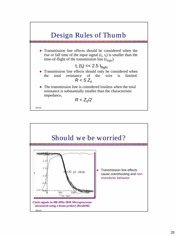
Should we be worried?
l Transmission line effects cause overshooting and non-monotonic behavior
Clock signals in 400 MHz IBM Microprocessor(measured using e-beam prober) [Restle98]