Intel® Open Source HD Graphics and Intel Iris™ Graphics ... · Intel® Open Source HD Graphics...
25
Intel® Open Source HD Graphics and Intel Iris™ Graphics Programmer's Reference Manual For the 2014-2015 Intel Core™ Processors, Celeron™ Processors and Pentium™ Processors based on the "Broadwell" Platform Volume 12: PCIE Configuration Registers May 2015, Revision 1.0
Transcript of Intel® Open Source HD Graphics and Intel Iris™ Graphics ... · Intel® Open Source HD Graphics...
Intel® Open Source HD Graphics and Intel Iris™ Graphics
Programmer's Reference Manual
For the 2014-2015 Intel Core™ Processors, Celeron™ Processors and Pentium™ Processors based on the "Broadwell" Platform
Volume 12: PCIE Configuration Registers
May 2015, Revision 1.0
PCIE Configuration Registers
ii Doc Ref # IHD-OS-BDW-Vol 12-05.15
Creative Commons License
You are free to Share - to copy, distribute, display, and perform the work under the following conditions:
• Attribution. You must attribute the work in the manner specified by the author or licensor (but not in any way that suggests that they endorse you or your use of the work).
• No Derivative Works. You may not alter, transform, or build upon this work.
Notices and Disclaimers
INFORMATION IN THIS DOCUMENT IS PROVIDED IN CONNECTION WITH INTEL® PRODUCTS. NO LICENSE, EXPRESS OR IMPLIED, BY ESTOPPEL OR OTHERWISE, TO ANY INTELLECTUAL PROPERTY RIGHTS IS GRANTED BY THIS DOCUMENT. EXCEPT AS PROVIDED IN INTEL'S TERMS AND CONDITIONS OF SALE FOR SUCH PRODUCTS, INTEL ASSUMES NO LIABILITY WHATSOEVER AND INTEL DISCLAIMS ANY EXPRESS OR IMPLIED WARRANTY, RELATING TO SALE AND/OR USE OF INTEL PRODUCTS INCLUDING LIABILITY OR WARRANTIES RELATING TO FITNESS FOR A PARTICULAR PURPOSE, MERCHANTABILITY, OR INFRINGEMENT OF ANY PATENT, COPYRIGHT OR OTHER INTELLECTUAL PROPERTY RIGHT.
A "Mission Critical Application" is any application in which failure of the Intel Product could result, directly or indirectly, in personal injury or death. SHOULD YOU PURCHASE OR USE INTEL'S PRODUCTS FOR ANY SUCH MISSION CRITICAL APPLICATION, YOU SHALL INDEMNIFY AND HOLD INTEL AND ITS SUBSIDIARIES, SUBCONTRACTORS AND AFFILIATES, AND THE DIRECTORS, OFFICERS, AND EMPLOYEES OF EACH, HARMLESS AGAINST ALL CLAIMS COSTS, DAMAGES, AND EXPENSES AND REASONABLE ATTORNEYS' FEES ARISING OUT OF, DIRECTLY OR INDIRECTLY, ANY CLAIM OF PRODUCT LIABILITY, PERSONAL INJURY, OR DEATH ARISING IN ANY WAY OUT OF SUCH MISSION CRITICAL APPLICATION, WHETHER OR NOT INTEL OR ITS SUBCONTRACTOR WAS NEGLIGENT IN THE DESIGN, MANUFACTURE, OR WARNING OF THE INTEL PRODUCT OR ANY OF ITS PARTS.
Intel may make changes to specifications and product descriptions at any time, without notice. Designers must not rely on the absence or characteristics of any features or instructions marked "reserved" or "undefined". Intel reserves these for future definition and shall have no responsibility whatsoever for conflicts or incompatibilities arising from future changes to them. The information here is subject to change without notice. Do not finalize a design with this information.
The products described in this document may contain design defects or errors known as errata which may cause the product to deviate from published specifications. Current characterized errata are available on request.
Implementations of the I2C bus/protocol may require licenses from various entities, including Philips Electronics N.V. and North American Philips Corporation.
Intel and the Intel logo are trademarks of Intel Corporation in the U.S. and other countries.
* Other names and brands may be claimed as the property of others.
Copyright © 2015, Intel Corporation. All rights reserved.

PCIE Configuration Registers
Doc Ref # IHD-OS-BDW-Vol 12-05.15 iii
Table of Contents
GFX PCI Registers .......................................................................................................................... 1
GTTMMADR .............................................................................................................................................................. 3
MSA Registers ..................................................................................................................................................... 3
MPGFXTRK_CR_DPFC_CONTROL_SA_0_2_0_GTTMMADR ............................................................ 3
MPGFXTRK_CR_DPFC_CPU_FENCE_OFFSET_0_2_0_GTTMMADR ............................................... 4
MPGFXTRK_CR_TILECTL_0_2_0_GTTMMADR ..................................................................................... 5
MPGFXTRK_CR_GFX_FLSH_CNTL_0_2_0_GTTMMADR .................................................................... 6
MPGFXTRK_CR_MTOLUD_0_2_0_GTTMMADR .................................................................................. 7
MPGFXTRK_CR_MGGC_0_2_0_GTTMMADR ....................................................................................... 9
MPGFXTRK_CR_MTOUUD_0_2_0_GTTMMADR ...............................................................................11
MPGFXTRK_CR_MBDSM_0_2_0_GTTMMADR ..................................................................................12
MPGFXTRK_CR_MBGSM_0_2_0_GTTMMADR ..................................................................................13
MPGFXTRK_CR_MGCMD_REG_0_2_0_GTTMMADR .......................................................................14
MPGFXTRK_CR_MEMRR_BASE_0_2_0_GTTMMADR ......................................................................19
MPGFXTRK_CR_MEMRR_MASK_0_2_0_GTTMMADR ....................................................................20
GSA Registers ....................................................................................................................................................21


PCIE Configuration Registers
Doc Ref # IHD-OS-BDW-Vol 12-05.15 1
GFX PCI Registers Address Space Address Symbol Name
PCI: 0/0/0 00050h GGC_0_0_0_PCI GMCH Graphics Control
PCI: 0/0/0 00054h DEVEN_0_0_0_PCI Device Enable
PCI: 0/0/0 000B0h BDSM_0_0_0_PCI Base Data of Stolen Memory
PCI: 0/0/0 000B4h BGSM_0_0_0_PCI Base of GTT Stolen Memory
PCI: 0/0/0 000E4h CAPID0_A_0_0_0_PCI Capabilities A
PCI: 0/0/0 000E8h CAPID0_B_0_0_0_PCI Capabilities B
PCI: 0/2/0 00000h VID2_0_2_0_PCI Vendor Identification
PCI: 0/2/0 00002h DID2_0_2_0_PCI Device Identification
PCI: 0/2/0 00004h PCICMD_0_2_0_PCI PCI Command
PCI: 0/2/0 00006h PCISTS2_0_2_0_PCI PCI Status
PCI: 0/2/0 00008h RID2_0_2_0_PCI Revision Identification
PCI: 0/2/0 00009h CC_0_2_0_PCI Class Code
PCI: 0/2/0 0000Ch CLS_0_2_0_PCI Cache Line Size
PCI: 0/2/0 0000Dh MLT2_0_2_0_PCI Master Latency Timer
PCI: 0/2/0 0000Eh HDR2_0_2_0_PCI Header Type
PCI: 0/2/0 00010h GTTMMADR_0_2_0_PCI Graphics Translation Table Memory Mapped Range Address
PCI: 0/2/0 00018h GMADR_0_2_0_PCI Graphics Memory Range Address
PCI: 0/2/0 00020h IOBAR_0_2_0_PCI I/O Base Address
PCI: 0/2/0 0002Ch SVID2_0_2_0_PCI Subsystem Vendor Identification
PCI: 0/2/0 0002Eh SID2_0_2_0_PCI Subsystem Identification
PCI: 0/2/0 00030h ROMADR_0_2_0_PCI Video BIOS ROM Base Address
PCI: 0/2/0 00034h CAPPOINT_0_2_0_PCI Capabilities Pointer
PCI: 0/2/0 0003Ch INTRLINE_0_2_0_PCI Interrupt Line
PCI: 0/2/0 0003Dh INTRPIN_0_2_0_PCI Interrupt Pin
PCI: 0/2/0 0003Eh MINGNT_0_2_0_PCI Minimum Grant
PCI: 0/2/0 0003Fh MAXLAT_0_2_0_PCI Maximum Latency
PCI: 0/2/0 00040h CAPID0_0_2_0_PCI Capability Identifier
PCI: 0/2/0 00042h CAPCTRL0_0_2_0_PCI Capabilities Control
PCI: 0/2/0 00044h CAPID0_A_0_2_0_PCI Mirror of Capabilities A
PCI: 0/2/0 00048h CAPID0_B_0_2_0_PCI Mirror of Capabilities B
PCI: 0/2/0 00050h MGGC0_0_2_0_PCI Mirror of GMCH Graphics Control
PCI: 0/2/0 00054h DEVEN0_0_2_0_PCI Mirror of Device Enable
PCI: 0/2/0 0005Ch BDSM_0_2_0_PCI Mirror of Base Data of Stolen Memory
PCI: 0/2/0 00060h HSRW_0_2_0_PCI Hardware Scratch Read Write

PCIE Configuration Registers
2 Doc Ref # IHD-OS-BDW-Vol 12-05.15
Address Space Address Symbol Name
PCI: 0/2/0 00062h MSAC_0_2_0_PCI Multi Size Aperture Control
PCI: 0/2/0 00090h MSI_CAPID_0_2_0_PCI Message Signaled Interrupts Capability ID
PCI: 0/2/0 00092h MC_0_2_0_PCI Message Control
PCI: 0/2/0 00094h MA_0_2_0_PCI Message Address
PCI: 0/2/0 00098h MD_0_2_0_PCI Message Data
PCI: 0/2/0 000A4h AFCIDNP_0_2_0_PCI Advanced Features Capabilities Identifier and Next Pointer
PCI: 0/2/0 000A6h AFLC_0_2_0_PCI Advanced Features Length and Capabilities
PCI: 0/2/0 000A8h AFCTL_0_2_0_PCI Advanced Features Control
PCI: 0/2/0 000A9h AFSTS_0_2_0_PCI Advanced Features Status
PCI: 0/2/0 000D0h PMCAPID_0_2_0_PCI Power Management Capabilities ID
PCI: 0/2/0 000D2h PMCAP_0_2_0_PCI Power Management Capabilities
PCI: 0/2/0 000D4h PMCS_0_2_0_PCI Power Management Control and Status
PCI: 0/2/0 000E0h SWSMI_0_2_0_PCI Software SMI
PCI: 0/2/0 000E4h GSE_0_2_0_PCI Graphics System Event
PCI: 0/2/0 000E8h SWSCI_0_2_0_PCI Software SCI
PCI: 0/2/0 000FCh ASLS_0_2_0_PCI ASL Storage
PCI: 0/2/0 00100h PASID_EXTCAP_0_2_0_PCI PASID Extended Capability Header
PCI: 0/2/0 00104h PASID_CAP_0_2_0_PCI PASID Capability
PCI: 0/2/0 00106h PASID_CTRL_0_2_0_PCI PASID Control
PCI: 0/2/0 00200h ATS_EXTCAP_0_2_0_PCI ATS Extended Capability Header
PCI: 0/2/0 00204h ATS_CAP_0_2_0_PCI ATS Capability
PCI: 0/2/0 00206h ATS_CTRL_0_2_0_PCI ATS Control
PCI: 0/2/0 00300h PR_EXTCAP_0_2_0_PCI Page Request Extended Capability Header
PCI: 0/2/0 00304h PR_CTRL_0_2_0_PCI Page Request Control
PCI: 0/2/0 00306h PR_STATUS_0_2_0_PCI Page Request Status
PCI: 0/2/0 00308h OPRC_0_2_0_PCI Outstanding Page Request Capacity
PCI: 0/2/0 0030Ch OPRA_0_2_0_PCI Outstanding Page Request Allocation

PCIE Configuration Registers
Doc Ref # IHD-OS-BDW-Vol 12-05.15 3
GTTMMADR MSA Registers MPGFXTRK_CR_DPFC_CONTROL_SA_0_2_0_GTTMMADR
B/D/F/Type: 0/2/0/GTTMMADR
Address Offset: 0x100100
Size: 32 bits
Access: RW
This register contains control bits related to Display Frame Buffer Compression Host Invalidation in System Agent.
Bit Type Default Value RST Type Description
29:29 RW 0x0 default/uncore/flr CPUFNCEN: 0: Display Buffer is not in a CPU fence. No modifications are allowed from CPU to the Display Buffer. 1: Display Buffer exists in a CPU fence.
4:0 RW 0x0 default/uncore/flr CPUFNCNUM: This field specifies the CPU visible FENCE number corresponding to the placement of the uncompressed frame buffer.

PCIE Configuration Registers
4 Doc Ref # IHD-OS-BDW-Vol 12-05.15
MPGFXTRK_CR_DPFC_CPU_FENCE_OFFSET_0_2_0_GTTMMADR
B/D/F/Type: 0/2/0/GTTMMADR
Address Offset: 0x100104
Size: 32 bits
Access: RW
This register contains control bits related to Display Frame Buffer Compression Host Invalidation in System Agent.
Bit Type Default Value RST Type Description
21:0 RW 0x0 default/uncore/flr YFNCDISP: Y offset from the CPU fence to the Display Buffer base

PCIE Configuration Registers
Doc Ref # IHD-OS-BDW-Vol 12-05.15 5
MPGFXTRK_CR_TILECTL_0_2_0_GTTMMADR
B/D/F/Type: 0/2/0/GTTMMADR
Address Offset: 0x101000
Size: 32 bits
Access: RW
This register contains control functionality related to GFX Aperture Tiling.
Bit Type Default Value RST Type Description
3:3 RW 0x0 default/uncore/flr BKSNPDIS: This bit allows to disable backsnoop requests as a result of IA requests to the Aperture. 0: Snoops are sent for IA requests that hit the Aperture 1: Snoops are never sent for IA requests that hit the Aperture
2:2 RW 0x0 default/uncore/flr DISTLBPF: On Tile Y GFX TLB miss, the cacheline read from the GTT contains 16 PTEs. This bit indicates whether all 16 PTEs are required to be cached or only the PTE that was requested. 0 - Prefetch 15 entries into the GFX TLB in addition to the demand-based fetch for Tile Y 1 - Disable TLB prefetch for Tile Y
1:0 RW 0x0 default/uncore/flr SWZCTL: This register location is updated via GFX Driver prior to enabling DRAM accesses. The Driver needs to obtain the need for memory address swizzling via DRAM configuration registers and set the following bits. 00b - No Address Swizzling 01b - Address bit 6 needs to be swizzled for tiled surfaces 10b - Reserved 11b - Reserved

PCIE Configuration Registers
6 Doc Ref # IHD-OS-BDW-Vol 12-05.15
MPGFXTRK_CR_GFX_FLSH_CNTL_0_2_0_GTTMMADR
B/D/F/Type: 0/2/0/GTTMMADR
Address Offset: 0x101008
Size: 32 bits
Access: WO
This register is used to flush GFX TLBs in the System Agent.
Bit Type Default Value RST Type Description
0:0 WO 0x0 default/uncore GFX_FLSH_CNTL: A CPU write to this bit flushes the GFX TLBs in the System Agent. The data associated with the write is discarded and a read returns all 0s.

PCIE Configuration Registers
Doc Ref # IHD-OS-BDW-Vol 12-05.15 7
MPGFXTRK_CR_MTOLUD_0_2_0_GTTMMADR
B/D/F/Type: 0/2/0/GTTMMADR
Address Offset: 0x108000
Size: 32 bits
Access: RO_V
This 32 bit register defines the Top of Low Usable DRAM. TSEG, GTT Graphics memory and Graphics Stolen Memory are within the DRAM space defined. From the top, the Host optionally claims 1 to 64MBs of DRAM for internal graphics if enabled, 1or 2MB of DRAM for GTT Graphics Stolen Memory if enabled and 1, 2, or 8 MB of DRAM for TSEG if enabled.
Programming Example:
C1DRB3 is set to 4GB
TSEG is enabled and TSEG size is set to 1MB
Internal Graphics is enabled, and Graphics Mode Select is set to 32MB
GTT Graphics Stolen Memory Size set to 2MB
BIOS knows the OS requires 1G of PCI space.
BIOS also knows the range from 0FEC00000h to 0FFFFFFFFh is not usable by the system. This 20MB range at the very top of addressable memory space is lost to APIC and LT.
According to the above equation, TOLUD is originally calculated to: 4GB 100000000h
The system memory requirements are: 4GB max addressable space - 1GB pci space - 35MB lost memory 3GB - 35MB minimum granularity 0ECB00000h
Since 0ECB00000h PCI and other system requirements is less than 100000000h, TOLUD should be programmed to ECBh.
These bits are Intel TXT lockable.

PCIE Configuration Registers
8 Doc Ref # IHD-OS-BDW-Vol 12-05.15
MPGFXTRK_CR_MTOLUD_0_2_0_GTTMMADR
Bit Type Default Value RST Type Description
31:20 RO_V 0x1 default/uncore TOLUD: This register contains bits 31 to 20 of an address one byte above the maximum DRAM memory below 4G that is usable by the operating system. Address bits 31 down to 20 programmed to 01h implies a minimum memory size of 1MB. Configuration software must set this value to the smaller of the following 2 choices: maximum amount memory in the system minus ME stolen memory plus one byte or the minimum address allocated for PCI memory. Address bits 19:0 are assumed to be 00000h for the purposes of address comparison. The Host interface positively decodes an address towards DRAM if the incoming address is less than the value programmed in this register. The Top of Low Usable DRAM is the lowest address above both Graphics Stolen memory and Tseg. BIOS determines the base of Graphics Stolen Memory by subtracting the Graphics Stolen Memory Size from TOLUD and further decrements by Tseg size to determine base of Tseg. This register must be 1MB aligned when reclaim is enabled.
0:0 RO_V 0x0 default/uncore LOCK: This bit will lock all writeable settings in this register, including itself.

PCIE Configuration Registers
Doc Ref # IHD-OS-BDW-Vol 12-05.15 9
MPGFXTRK_CR_MGGC_0_2_0_GTTMMADR
B/D/F/Type: 0/2/0/GTTMMADR
Address Offset: 0x108040
Size: 16 bits
Access: RO_V
All the bits in this register are Intel TXT lockable.
Bit Type Default Value RST Type Description
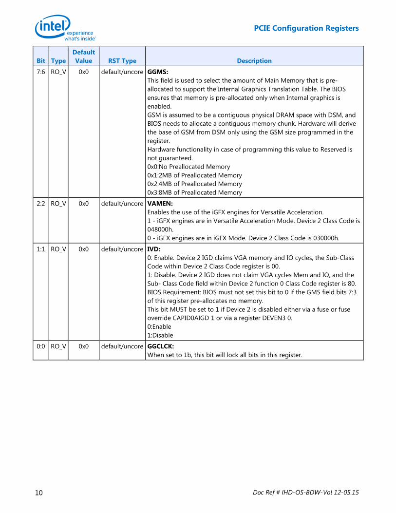
15:8 RO_V 0x5 default/uncore GMS: This field is used to select the amount of Main Memory that is pre-allocated to support the Internal Graphics device in VGA (non-linear) and Native (linear) modes. The BIOS ensures that memory is pre-allocated only when Internal graphics is enabled. Hardware does not clear or set any of these bits automatically based on IGD being disabled/enabled. BIOS Requirement: BIOS must not set this field to 0h if IVD (bit 1 of this register) is 0. 00h:0MB 01h:32MB 02h:64MB 03h:96MB 04h:128MB 05h:160MB (default) 06h:192MB 07h:224MB 08h:256MB 09h:288MB 0Ah:320MB 0Bh:352MB 0Ch:384MB 0Dh:416MB 0Eh:448MB 0Fh:480MB 10h:512MB 11h - 1Fh: Reserved 20h:1024MB 21h - 2Fh: Reserved 30h:1536MB 31h - 3Eh: Reserved 3Fh: 2016MB 40h - FFh: Reserved Hardware functionality in case of programming this value to Reserved is not guaranteed.
PCIE Configuration Registers
10 Doc Ref # IHD-OS-BDW-Vol 12-05.15
Bit Type Default Value RST Type Description
7:6 RO_V 0x0 default/uncore GGMS: This field is used to select the amount of Main Memory that is pre-allocated to support the Internal Graphics Translation Table. The BIOS ensures that memory is pre-allocated only when Internal graphics is enabled. GSM is assumed to be a contiguous physical DRAM space with DSM, and BIOS needs to allocate a contiguous memory chunk. Hardware will derive the base of GSM from DSM only using the GSM size programmed in the register. Hardware functionality in case of programming this value to Reserved is not guaranteed. 0x0:No Preallocated Memory 0x1:2MB of Preallocated Memory 0x2:4MB of Preallocated Memory 0x3:8MB of Preallocated Memory
2:2 RO_V 0x0 default/uncore VAMEN: Enables the use of the iGFX engines for Versatile Acceleration. 1 - iGFX engines are in Versatile Acceleration Mode. Device 2 Class Code is 048000h. 0 - iGFX engines are in iGFX Mode. Device 2 Class Code is 030000h.
1:1 RO_V 0x0 default/uncore IVD: 0: Enable. Device 2 IGD claims VGA memory and IO cycles, the Sub-Class Code within Device 2 Class Code register is 00. 1: Disable. Device 2 IGD does not claim VGA cycles Mem and IO, and the Sub- Class Code field within Device 2 function 0 Class Code register is 80. BIOS Requirement: BIOS must not set this bit to 0 if the GMS field bits 7:3 of this register pre-allocates no memory. This bit MUST be set to 1 if Device 2 is disabled either via a fuse or fuse override CAPID0AIGD 1 or via a register DEVEN3 0. 0:Enable 1:Disable
0:0 RO_V 0x0 default/uncore GGCLCK: When set to 1b, this bit will lock all bits in this register.

PCIE Configuration Registers
Doc Ref # IHD-OS-BDW-Vol 12-05.15 11
MPGFXTRK_CR_MTOUUD_0_2_0_GTTMMADR
B/D/F/Type: 0/2/0/GTTMMADR
Address Offset: 0x108080
Size: 64 bits
Access: RO_V
This 64 bit register defines the Top of Upper Usable DRAM.
Configuration software must set this value to TOM minus all ME stolen memory if reclaim is disabled. If reclaim is enabled, this value must be set to reclaim limit 1byte, 1MB aligned, since reclaim limit is 1MB aligned. Address bits 19:0 are assumed to be 0000000h for the purposes of address comparison. The Host interface positively decodes an address towards DRAM if the incoming address is less than the value programmed in this register and greater than or equal to 4GB.
BIOS Restriction: Minimum value for TOUUD is 4GB.
These bits are Intel TXT lockable.
Bit Type Default Value RST Type Description
38:20 RO_V 0x0 default/uncore TOUUD: This register contains bits 38 to 20 of an address one byte above the maximum DRAM memory above 4G that is usable by the operating system. Configuration software must set this value to TOM minus all ME stolen memory if reclaim is disabled. If reclaim is enabled, this value must be set to reclaim limit 1MB aligned since reclaim limit 1byte is 1MB aligned. Address bits 19:0 are assumed to be 0000000h for the purposes of address comparison. The Host interface positively decodes an address towards DRAM if the incoming address is less than the value programmed in this register and greater than 4GB.
0:0 RO_V 0x0 default/uncore LOCK: This bit will lock all writeable settings in this register, including itself.

PCIE Configuration Registers
12 Doc Ref # IHD-OS-BDW-Vol 12-05.15
MPGFXTRK_CR_MBDSM_0_2_0_GTTMMADR
B/D/F/Type: 0/2/0/GTTMMADR
Address Offset: 0x1080c0
Size: 32 bits
Access: RO_V
This register contains the base address of graphics data stolen DRAM memory. BIOS determines the base of graphics data stolen memory by subtracting the graphics data stolen memory size PCI Device 0 offset 52 bits 7:4 from TOLUD PCI Device 0 offset BC bits 31:20.
Bit Type Default Value RST Type Description
31:20 RO_V 0x0 default/uncore BDSM: This register contains bits 31 to 20 of the base address of stolen DRAM memory. BIOS determines the base of graphics stolen memory by subtracting the graphics stolen memory size PCI Device 0 offset 52 bits 6:4 from TOLUD PCI Device 0 offset BC bits 31:20.
0:0 RO_V 0x0 default/uncore LOCK: This bit will lock all writeable settings in this register, including itself.
PCIE Configuration Registers
Doc Ref # IHD-OS-BDW-Vol 12-05.15 13
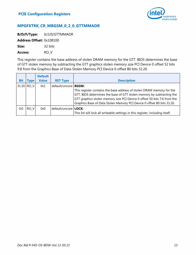
MPGFXTRK_CR_MBGSM_0_2_0_GTTMMADR
B/D/F/Type: 0/2/0/GTTMMADR
Address Offset: 0x108100
Size: 32 bits
Access: RO_V
This register contains the base address of stolen DRAM memory for the GTT. BIOS determines the base of GTT stolen memory by subtracting the GTT graphics stolen memory size PCI Device 0 offset 52 bits 9:8 from the Graphics Base of Data Stolen Memory PCI Device 0 offset B0 bits 31:20.
Bit Type Default Value RST Type Description
31:20 RO_V 0x1 default/uncore BGSM: This register contains the base address of stolen DRAM memory for the GTT. BIOS determines the base of GTT stolen memory by subtracting the GTT graphics stolen memory size PCI Device 0 offset 50 bits 7:6 from the Graphics Base of Data Stolen Memory PCI Device 0 offset B0 bits 31:20.
0:0 RO_V 0x0 default/uncore LOCK: This bit will lock all writeable settings in this register, including itself.

PCIE Configuration Registers
14 Doc Ref # IHD-OS-BDW-Vol 12-05.15
MPGFXTRK_CR_MGCMD_REG_0_2_0_GTTMMADR
B/D/F/Type: 0/2/0/GTTMMADR
Address Offset: 0x108300
Size: 32 bits
Access: RO_V/RO/WO
Register to control remapping hardware. If multiple control fields in this register need to be modified, software must serialize the modifications through multiple writes to this register.
Bit Type Default Value RST Type Description
31:31 RO_V 0x0 default/uncore TE: Software writes to this field to request hardware to enabledisable DMA-remapping: 0: Disable DMA remapping 1: Enable DMA remapping Hardware reports the status of the translation enable operation through the TES field in the Global Status register. There may be active DMA requests in the platform when software updates this field. Hardware must enable or disable remapping logic only at deterministic transaction boundaries, so that any in-flight transaction is either subject to remapping or not at all. Hardware implementations supporting DMA draining must drain any in-flight DMA readwrite requests queued within the Root-Complex before completing the translation enable command and reflecting the status of the command through the TES field in the Global Status register. The value returned on a read of this field is undefined.

PCIE Configuration Registers
Doc Ref # IHD-OS-BDW-Vol 12-05.15 15
Bit Type Default Value RST Type Description
30:30 WO 0x0 default/uncore SRTP: Software sets this field to setupdate the root-entry table pointer used by hardware. The root-entry table pointer is specified through the Root-entry Table Address RTAREG register. Hardware reports the status of the "Set Root Table Pointer" operation through the RTPS field in the Global Status register. The "Set Root Table Pointer" operation must be performed before enabling or re-enabling after disabling DMA remapping through the TE field. After a "Set Root Table Pointer" operation, software must globally invalidate the context cache and then globally invalidate of IOTLB. This is required to ensure hardware uses only the remapping structures referenced by the new root table pointer, and not stale cached entries. While DMA remapping hardware is active, software may update the root table pointer through this field. However, to ensure valid in-flight DMA requests are deterministically remapped, software must ensure that the structures referenced by the new root table pointer are programmed to provide the same remapping results as the structures referenced by the previous root-table pointer. Clearing this bit has no effect. The value returned on read of this field is undefined.
29:29 RO 0x0 default/uncore SFL: This field is valid only for implementations supporting advanced fault logging. Software sets this field to request hardware to setupdate the fault-log pointer used by hardware. The fault-log pointer is specified through Advanced Fault Log register. Hardware reports the status of the 'Set Fault Log' operation through the FLS field in the Global Status register. The fault log pointer must be set before enabling advanced fault logging through EAFL field. Once advanced fault logging is enabled, the fault log pointer may be updated through this field while DMA remapping is active. Clearing this bit has no effect. The value returned on read of this field is undefined.
PCIE Configuration Registers
16 Doc Ref # IHD-OS-BDW-Vol 12-05.15
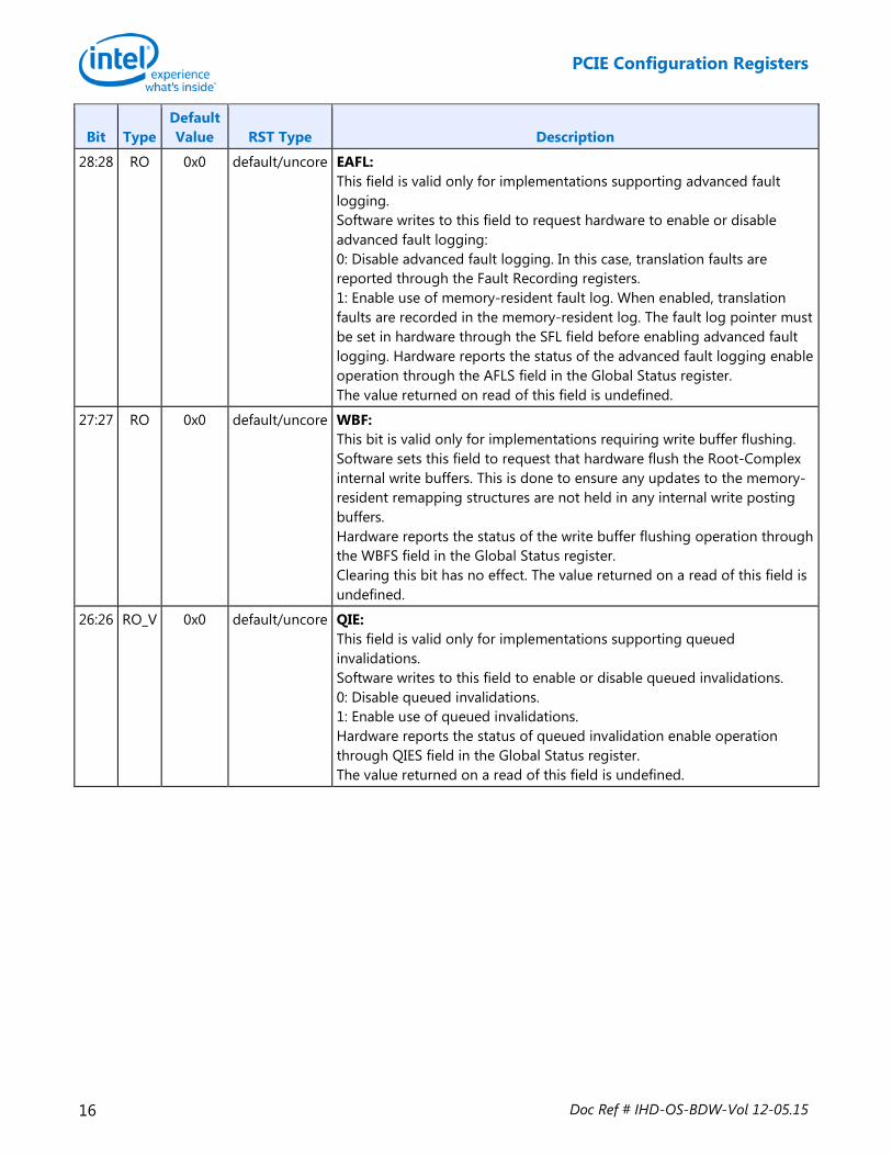
Bit Type Default Value RST Type Description
28:28 RO 0x0 default/uncore EAFL: This field is valid only for implementations supporting advanced fault logging. Software writes to this field to request hardware to enable or disable advanced fault logging: 0: Disable advanced fault logging. In this case, translation faults are reported through the Fault Recording registers. 1: Enable use of memory-resident fault log. When enabled, translation faults are recorded in the memory-resident log. The fault log pointer must be set in hardware through the SFL field before enabling advanced fault logging. Hardware reports the status of the advanced fault logging enable operation through the AFLS field in the Global Status register. The value returned on read of this field is undefined.
27:27 RO 0x0 default/uncore WBF: This bit is valid only for implementations requiring write buffer flushing. Software sets this field to request that hardware flush the Root-Complex internal write buffers. This is done to ensure any updates to the memory-resident remapping structures are not held in any internal write posting buffers. Hardware reports the status of the write buffer flushing operation through the WBFS field in the Global Status register. Clearing this bit has no effect. The value returned on a read of this field is undefined.
26:26 RO_V 0x0 default/uncore QIE: This field is valid only for implementations supporting queued invalidations. Software writes to this field to enable or disable queued invalidations. 0: Disable queued invalidations. 1: Enable use of queued invalidations. Hardware reports the status of queued invalidation enable operation through QIES field in the Global Status register. The value returned on a read of this field is undefined.
PCIE Configuration Registers
Doc Ref # IHD-OS-BDW-Vol 12-05.15 17
Bit Type Default Value RST Type Description
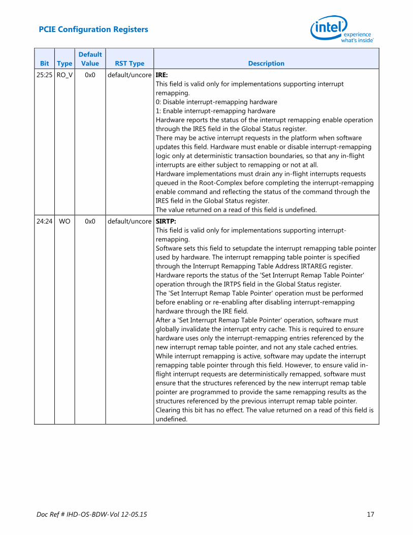
25:25 RO_V 0x0 default/uncore IRE: This field is valid only for implementations supporting interrupt remapping. 0: Disable interrupt-remapping hardware 1: Enable interrupt-remapping hardware Hardware reports the status of the interrupt remapping enable operation through the IRES field in the Global Status register. There may be active interrupt requests in the platform when software updates this field. Hardware must enable or disable interrupt-remapping logic only at deterministic transaction boundaries, so that any in-flight interrupts are either subject to remapping or not at all. Hardware implementations must drain any in-flight interrupts requests queued in the Root-Complex before completing the interrupt-remapping enable command and reflecting the status of the command through the IRES field in the Global Status register. The value returned on a read of this field is undefined.
24:24 WO 0x0 default/uncore SIRTP: This field is valid only for implementations supporting interrupt-remapping. Software sets this field to setupdate the interrupt remapping table pointer used by hardware. The interrupt remapping table pointer is specified through the Interrupt Remapping Table Address IRTAREG register. Hardware reports the status of the 'Set Interrupt Remap Table Pointer' operation through the IRTPS field in the Global Status register. The 'Set Interrupt Remap Table Pointer' operation must be performed before enabling or re-enabling after disabling interrupt-remapping hardware through the IRE field. After a 'Set Interrupt Remap Table Pointer' operation, software must globally invalidate the interrupt entry cache. This is required to ensure hardware uses only the interrupt-remapping entries referenced by the new interrupt remap table pointer, and not any stale cached entries. While interrupt remapping is active, software may update the interrupt remapping table pointer through this field. However, to ensure valid in-flight interrupt requests are deterministically remapped, software must ensure that the structures referenced by the new interrupt remap table pointer are programmed to provide the same remapping results as the structures referenced by the previous interrupt remap table pointer. Clearing this bit has no effect. The value returned on a read of this field is undefined.

PCIE Configuration Registers
18 Doc Ref # IHD-OS-BDW-Vol 12-05.15
Bit Type Default Value RST Type Description
23:23 RO_V 0x0 default/uncore CFI: This field is valid only for Intel64 implementations supporting interrupt-remapping. Software writes to this field to enable or disable Compatibility Format interrupts on Intel64 platforms. The value in this field is effective only when interrupt-remapping is enabled and Extended Interrupt Mode x2APIC mode is not enabled. 0: Block Compatibility format interrupts. 1: Process Compatibility format interrupts as pass-through bypass interrupt remapping. Hardware reports the status of updating this field through the CFIS field in the Global Status register. The value returned on a read of this field is undefined.
PCIE Configuration Registers
Doc Ref # IHD-OS-BDW-Vol 12-05.15 19
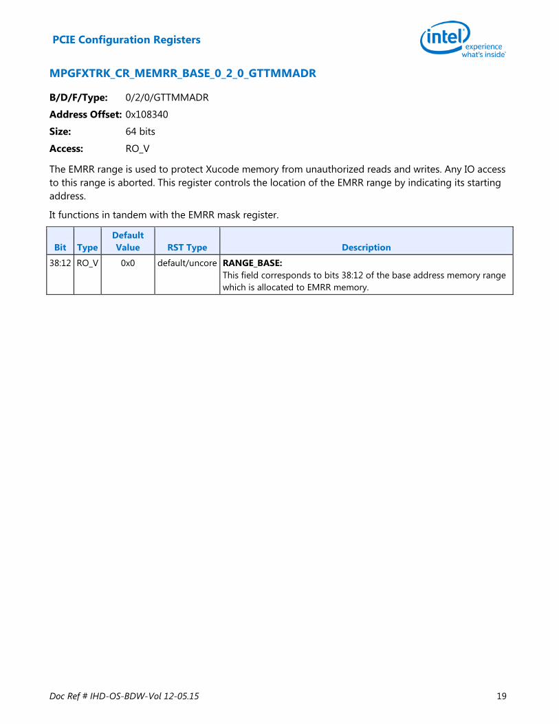
MPGFXTRK_CR_MEMRR_BASE_0_2_0_GTTMMADR
B/D/F/Type: 0/2/0/GTTMMADR
Address Offset: 0x108340
Size: 64 bits
Access: RO_V
The EMRR range is used to protect Xucode memory from unauthorized reads and writes. Any IO access to this range is aborted. This register controls the location of the EMRR range by indicating its starting address.
It functions in tandem with the EMRR mask register.
Bit Type Default Value RST Type Description
38:12 RO_V 0x0 default/uncore RANGE_BASE: This field corresponds to bits 38:12 of the base address memory range which is allocated to EMRR memory.

PCIE Configuration Registers
20 Doc Ref # IHD-OS-BDW-Vol 12-05.15
MPGFXTRK_CR_MEMRR_MASK_0_2_0_GTTMMADR
B/D/F/Type: 0/2/0/GTTMMADR
Address Offset: 0x108380
Size: 64 bits
Access: RO_V
This register controls the size of the EMRR range by indicating which address bits must match the EMRR base register value.
Bit Type Default Value RST Type Description
38:12 RO_V 0x0 default/uncore RANGE_MASK: This field indicates which address bits must match EMRR base in order to qualify as an EMRR access.
11:11 RO_V 0x0 default/uncore RANGE_EN: Indicates whether the EMRR range is enabled and valid.
10:10 RO_V 0x0 default/uncore LOCK: Setting this bit locks all writeable settings in this register, including itself.

PCIE Configuration Registers
Doc Ref # IHD-OS-BDW-Vol 12-05.15 21
GSA Registers
Address Space Address Symbol Name
MMIO: 0/2/0 130040h LCPLL_CTL LCPLL Control
MMIO: 0/2/0 130044h GTSP1_0_2_0_GTTMMADR GT Scratch Pad 1
MMIO: 0/2/0 130048h GTSP2_0_2_0_GTTMMADR GT Scratch Pad 2
MMIO: 0/2/0 13004Ch GTSP3_0_2_0_GTTMMADR GT Scratch Pad 3
MMIO: 0/2/0 130050h GTSP4_0_2_0_GTTMMADR GT Scratch Pad 4
MMIO: 0/2/0 130054h GTSP5_0_2_0_GTTMMADR GT Scratch Pad 5
MMIO: 0/2/0 130058h GTSP6_0_2_0_GTTMMADR GT Scratch Pad 6
MMIO: 0/2/0 13005Ch GTSP7_0_2_0_GTTMMADR GT Scratch Pad 7
MMIO: 0/2/0 130090h GTFORCEAWAKE_0_2_0_GTTMMADR GT Force Awake