Intel 88CO196EC CHMOS 16-Bit Microcontroller Sheets/Intel PDFs...2 Product Nomenclature.....8 3...
44
Intel ® 88CO196EC CHMOS 16-Bit Microcontroller Datasheet Product Features The Intel ® 88CO196EC CHMOS 16-Bit Microcontroller is the first member of the MCS ® 96 family of microcontrollers to integrate flash memory on-chip. The Intel® 88CO196EC, with its integrated flash memory, brings a new level of integration that offers embedded system designers cost-effective solutions. • 256 Kbytes on-chip flash program memory • 40 MHz operation • Optional clock quadrupler • Programmable clock output signal (CLKOUT) • 2 Mbytes of linear address space • 1.25 Kbytes of register RAM • 2.75 Kbytes of code RAM • Register-to-register architecture • Stack overflow/underflow monitor with user-defined upper and lower stack pointer boundary limits • Two peripheral interrupt handlers (PIHs) provide direct hardware handling of up to 45 interrupts • Up to 59 I/O port pins • Full-duplex serial port with dedicated baud-rate generator • Enhanced synchronous serial I/O unit (SSIO) • 16 10-bit A/D channels with auto-scan mode and dedicated results registers • Controller area network (CAN) 2.0 networking protocol • Serial debug unit provides read and write access to code RAM with no CPU overhead • Chip-select unit (CSU) — Three chip-select pins — Dynamic demultiplexed/multiplexed address/data bus for each chip-select — Programmable wait states (0, 1, 2, or 3) for each chip-select — Programmable bus width (8- or 16-bit) for each chip-select — Programmable address range for each chip-select • Event processor array (EPA) — Two flexible 16-bit timer/counters — Five high-speed capture/compare channels with a lock feature for noise filtering — 10 enhanced high-speed capture/compare channels with period and duty cycle measurement capability, as well as a lock feature for noise filtering • Complete system development support • Packaging — 132-pin PQFP • Temperature Offerings — Commercial (0C - 70C) — Extended (-40C - 85C) Order Number: 273970-002 August, 2004
Transcript of Intel 88CO196EC CHMOS 16-Bit Microcontroller Sheets/Intel PDFs...2 Product Nomenclature.....8 3...

Intel® 88CO196EC CHMOS 16-Bit Microcontroller
Datasheet
Product Features
The Intel® 88CO196EC CHMOS 16-Bit Microcontroller is the first member of the MCS®96 family of microcontrollers to integrate flash memory on-chip. The Intel® 88CO196EC, with its integrated flash memory, brings a new level of integration that offers embedded system designers cost-effective solutions.
• 256 Kbytes on-chip flash program memory
• 40 MHz operation
• Optional clock quadrupler
• Programmable clock output signal (CLKOUT)
• 2 Mbytes of linear address space
• 1.25 Kbytes of register RAM
• 2.75 Kbytes of code RAM
• Register-to-register architecture
• Stack overflow/underflow monitor with user-defined upper and lower stack pointer boundary limits
• Two peripheral interrupt handlers (PIHs) provide direct hardware handling of up to 45 interrupts
• Up to 59 I/O port pins
• Full-duplex serial port with dedicated baud-rate generator
• Enhanced synchronous serial I/O unit (SSIO)
• 16 10-bit A/D channels with auto-scan mode and dedicated results registers
• Controller area network (CAN) 2.0 networking protocol
• Serial debug unit provides read and write access to code RAM with no CPU overhead
• Chip-select unit (CSU)
— Three chip-select pins
— Dynamic demultiplexed/multiplexed address/data bus for each chip-select
— Programmable wait states (0, 1, 2, or 3) for each chip-select
— Programmable bus width (8- or 16-bit) for each chip-select
— Programmable address range for each chip-select
• Event processor array (EPA)
— Two flexible 16-bit timer/counters
— Five high-speed capture/compare channels with a lock feature for noise filtering
— 10 enhanced high-speed capture/compare channels with period and duty cycle measurement capability, as well as a lock feature for noise filtering
• Complete system development support
• Packaging
— 132-pin PQFP
• Temperature Offerings
— Commercial (0C - 70C)
— Extended (-40C - 85C)
Order Number: 273970-002 August, 2004

INFORMATION IN THIS DOCUMENT IS PROVIDED IN CONNECTION WITH INTEL® PRODUCTS. NO LICENSE, EXPRESS OR IMPLIED, BY ESTOPPEL OR OTHERWISE, TO ANY INTELLECTUAL PROPERTY RIGHTS IS GRANTED BY THIS DOCUMENT. EXCEPT AS PROVIDED IN INTEL'S TERMS AND CONDITIONS OF SALE FOR SUCH PRODUCTS, INTEL ASSUMES NO LIABILITY WHATSOEVER, AND INTEL DISCLAIMS ANY EXPRESS OR IMPLIED WARRANTY, RELATING TO SALE AND/OR USE OF INTEL PRODUCTS INCLUDING LIABILITY OR WARRANTIES RELATING TO FITNESS FOR A PARTICULAR PURPOSE, MERCHANTABILITY, OR INFRINGEMENT OF ANY PATENT, COPYRIGHT OR OTHER INTELLECTUAL PROPERTY RIGHT. Intel products are not intended for use in medical, life saving, life sustaining applications.
Intel may make changes to specifications and product descriptions at any time, without notice.
Designers must not rely on the absence or characteristics of any features or instructions marked “reserved” or “undefined.” Intel reserves these for future definition and shall have no responsibility whatsoever for conflicts or incompatibilities arising from future changes to them.
The Intel® 88CO196EC CHMOS 16-Bit Microcontroller may contain design defects or errors known as errata which may cause the product to deviate from published specifications. Current characterized errata are available on request.
Contact your local Intel sales office or your distributor to obtain the latest specifications and before placing your product order.
Copies of documents which have an ordering number and are referenced in this document, or other Intel literature may be obtained by calling 1-800-548-4725 or by visiting Intel's website at http://www.intel.com.
AnyPoint, AppChoice, BoardWatch, BunnyPeople, CablePort, Celeron, Chips, CT Media, Dialogic, DM3, EtherExpress, ETOX, FlashFile, i386, i486, i960, iCOMP, InstantIP, Intel, Intel Centrino, Intel logo, Intel386, Intel486, Intel740, IntelDX2, IntelDX4, IntelSX2, Intel Create & Share, Intel GigaBlade, Intel InBusiness, Intel Inside, Intel Inside logo, Intel NetBurst, Intel NetMerge, Intel NetStructure, Intel Play, Intel Play logo, Intel SingleDriver, Intel SpeedStep, Intel StrataFlash, Intel TeamStation, Intel Xeon, Intel XScale, IPLink, Itanium, MCS, MMX, MMX logo, Optimizer logo, OverDrive, Paragon, PC Dads, PC Parents, PDCharm, Pentium, Pentium II Xeon, Pentium III Xeon, Performance at Your Command, RemoteExpress, SmartDie, Solutions960, Sound Mark, StorageExpress, The Computer Inside., The Journey Inside, TokenExpress, VoiceBrick, VTune, and Xircom are trademarks or registered trademarks of Intel Corporation or its subsidiaries in the United States and other countries.
*Other names and brands may be claimed as the property of others.
Copyright © February, 2004, Intel Corporation

3
Intel® 88CO196EC
Contents1.0 Product Overview ...............................................................................................................7
1.1 Nomenclature Overview ........................................................................................8
2.0 Pinout .................................................................................................................................9
3.0 Signals..............................................................................................................................11
4.0 Address Map ....................................................................................................................21
5.0 Electrical Characteristics ..................................................................................................23
5.1 DC Characteristics ..............................................................................................23
6.0 Explanation of AC Symbols..............................................................................................25
6.1 AC Characteristics — Multiplexed Bus Mode......................................................266.2 AC Characteristics — Demultiplexed Bus Mode .................................................306.3 Deferred Bus Timing Mode .................................................................................346.4 AC Characteristics — Serial Port, Mode 0 ..........................................................356.5 AC Characteristics — Synchronous Serial Port ..................................................366.6 AC Characteristics — Serial Debug Unit.............................................................376.7 A/D Sample and Conversion Times ....................................................................38
6.7.1 AC Characteristics — A/D Converter, 10-Bit Mode................................396.7.2 AC Characteristics — A/D Converter, 8-Bit Mode..................................40
6.8 External Clock Drive............................................................................................416.9 Test Output Waveforms ......................................................................................426.10 Flash Memory Erase Performance......................................................................42
7.0 Thermal Characteristics ...................................................................................................43
Figures1 Intel® 88CO196EC CHMOS 16-Bit Microcontroller Block Diagram ......................72 Product Nomenclature...........................................................................................83 Intel® 88CO196EC CHMOS 16-Bit Microcontroller 132-Pin PQFP Package........94 System Bus Timing Diagram (Multiplexed Bus Mode) ........................................285 READY Timing Diagram (Multiplexed Bus Mode)...............................................296 System Bus Timing Diagram (Demultiplexed Bus Mode) ...................................327 READY Timing Diagram (Demultiplexed Bus Mode) ..........................................338 Deferred Bus Mode Timing Diagram...................................................................349 Serial Port Waveform — Mode............................................................................3510 Synchronous Serial Port......................................................................................3611 Serial Debug Unit ................................................................................................3712 External Clock Drive Waveforms.........................................................................4113 AC Testing Output Waveforms............................................................................4214 Float Waveforms During 5.0 Volt Testing............................................................42

Intel® 88CO196EC
4
Tables1 Description of Product Nomenclature ................................................................... 82 Intel® 88CO196EC CHMOS 16-Bit Microcontroller
132-Pin PQFP Package Pin Assignments .......................................................... 103 Signal Descriptions ............................................................................................. 114 Intel® 88CO196EC CHMOS 16-Bit Microcontroller Address Map.......................215 DC Characteristics at Vcc = 4.75 V – 5.25 V ....................................................... 236 AC Timing Symbol Definitions............................................................................. 257 AC Characteristics, Multiplexed Bus Mode ......................................................... 268 AC Characteristics, Demultiplexed Bus Mode .................................................... 309 Serial Port Timing — Mode 0†............................................................................. 3510 Synchronous Serial Port Timing.......................................................................... 3611 Serial Debug Unit Timing .................................................................................... 3712 10-bit A/D Operating Conditions ......................................................................... 3913 10-Bit Mode A/D Characteristics Over Specified Operating Conditions.............. 3914 8-Bit A/D Operating Conditions ...........................................................................4015 8-Bit Mode A/D Characteristics Over Specified Operating Conditions................4016 External Clock Drive............................................................................................ 4117 Flash Memory Erase Performance ..................................................................... 4218 Thermal Characteristics ...................................................................................... 43

5
Intel® 88CO196EC
Revision History
Date Revision Description
February 2004 001 Initial release
August 2004 002 To address the fact that many of the package prefix variables have changed, all package prefix variables in this document are now indicated with an "x".

Intel® 88CO196EC
6

Intel® 88CO196EC
Datasheet 7
1.0 Product Overview
The Intel® 88CO196EC CHMOS 16-Bit Microcontroller is highly integrated with an enhanced peripheral set. The integrated CAN 2.0 networking protocol provides for efficient communication to a high-speed CAN bus. The serial debug unit (SDU) provides system debug and development capabilities. The SDU can set a single hardware breakpoint. In addition, the SDU provides read and write access to code RAM through a high-speed, dedicated serial link. A stack overflow/underflow monitor assists in code development by causing a nonmaskable interrupt if the stack pointer crosses a user-defined boundary. The 16-channel A/D converter supports an auto-scan mode that operates with no CPU overhead. Each A/D channel has a dedicated result register. The EPA supports high-speed event captures and output compares with 15 programmable, high-speed channels.
Figure 1. Intel® 88CO196EC CHMOS 16-Bit Microcontroller Block Diagram
Code/DataRAM
2.75 Kbytes
Port 6
Queue
A20:16
Source (16)
Destination (16)
AD15:0
SIOBaud-rateGenerator
EPA 2 Timers
Ports 7,8
5 Capture/Compares
A/DConverter
BusController
A15:0
Serial DebugUnit
WatchdogTimer
StackOverflowModule
CAN SSIO0SSIO1
Flash256 Kbytes
A4324-01
Port 9
Bus-ControlInterface Unit
MicrocodeEngine
Chip-selectUnit
PeripheralTransaction
Server
MemoryInterface
Unit
RegisterRAM
1.25 KbytesALU
InterruptController
PeripheralInterruptHandler
Bus Control
Peripheral Addr Bus (10)
Peripheral Data Bus (16)
Mem
ory
Add
r B
us (
24)
Port 3,4,5
10 EnhancedCapture/
Compares
Port 2
Mem
ory
Dat
a B
us (
16)

Intel® 88CO196EC
8 Datasheet
1.1 Nomenclature Overview
Figure 2. Product Nomenclature
Table 1. Description of Product Nomenclature
Parameter Options Description
Temperature Options xx
Commercial temperature range (0° C to 70° C case) Extended temperature range (–40° C to 85° C case)
Program-Memory x Internal flash memory
Process Information C CHMOS
Product Type O Standard Embedded Product
Product Family 196EC
Device Speed no mark 40 MHz
B3165-01
Program M
emory O
ptions
XX8XX
Temperature
Process Information
XXXXX XX
Product TypeProduct Fam
ilyStepping Identifier
B M
B M
B M
B M
B M

Intel® 88CO196EC
Datasheet 9
2.0 Pinout
Figure 3. Intel® 88CO196EC CHMOS 16-Bit Microcontroller 132-Pin PQFP Package
B3055-01
123456789101112131415161718192021222324252627282930313233
999897969594939291908988878685848382818079787776757473727170696867
P3.3 / AD3 / PBUS3P3.4 / AD4 / PBUS4P3.5 / AD5 / PBUS5P3.6 / AD6 / PBUS6P3.7 / AD7 / PBUS7P4.0 / AD8 / PBUS8P4.1 / AD9 / PBUS9P4.2 / AD10 / PBUS10P4.3 / AD11 / PBUS11P4.4 / AD12 / PBUS12P4.5 / AD13 / PBUS13P4.6 / AD14 / PBUS14P4.7 / AD15 / PBUS15CRBUSY#CROUTCRDCLKVSSVPPCRINVSSVSSVSSPLLENVSSVCCA7A6A5A4A3A2A1A0
132
131
130
129
128
127
126
125
124
123
122
121
120
119
118
117
116
115
114
113
112
111
110
109
108
107
106
105
104
103
102
101
100
34 35 36 37 38 39 40 41 42 43 44 45 46 47 48 49 50 51 52 53 54 55 56 57 58 59 60 61 62 63 64 65 66
ACH7ACH8ACH9
ANGNDVREFVCCVSS
ACH10ACH11ACH12ACH13ACH14ACH15
VSSVCC
P8.0 / EPAPWM8 / BLK0#P8.1 / EPAPWM9 / BLK1#
P8.2 / EPA10 / T1CLK / BLK2#P8.3 / EPA11 / T1RST / BLK3#
P8.4 / EPA12 / T2CLKP8.5 / EPA13 / T2RST
P8.6 / EPA14P8.7VCCVSS
P7.0 / EPAPWM0P7.1 / EPAPWM1P7.2 / EPAPWM2P7.3 / EPAPWM3P7.4 / EPAPWM4P7.5 / EPAPWM5P7.6 / EPAPWM6P7.7 / EPAPWM7
AC
H6
AC
H5
AC
H4
AC
H3
AC
H2
AC
H1
AC
H0
VC
CV
SS
P2.
0 / T
XD
P2.
1 / R
XD
/ P
ALE
#P
2.2
/ EX
TIN
T /
PR
OG
#P
2.3
P2.
4 / A
INC
#P
2.5
P2.
6 / H
OLD
# / C
PV
ER
/ O
NC
E#
/ HLD
A#
P2.
7 / C
LKO
UT
/ P
AC
T#
VS
SV
CC
TX
CA
NR
XC
AN
P9.
2 / S
C0
P9.
3 / S
D0
P9.
4 / S
C1
/ CH
S#
P9.
5 / S
D1
P9.
6P
9.7
NM
IR
ES
ET
#E
A#
P3.
0 / A
D0
/ PB
US
0P
3.1
/ AD
1 / P
BU
S1
P3.
2 / A
D2
/ PB
US
2
A15
A14
A13
A12
VC
CV
SS
A11
P6.
0 / A
16 /
PB
US
16P
6.1
/ A17
/ PB
US
17P
6.2
/ A18
/ PB
US
18P
6.3
/ A19
/ PB
US
19P
6.4
/ A20
/ PB
US
20P
6.5
/ CS
0# /
PM
OD
E0
P6.
6 / C
S1#
/ PM
OD
E1
P6.
7 / C
S2#
/ PM
OD
E2
VS
SV
CC
P5.
0 / A
LE /
AD
V#
P5.
1 / I
NS
TP
5.2
/ WR
# / W
RL#
P5.
3 / R
D#
P5.
4 / B
RE
Q#
/ TM
OD
E0#
VS
SP
LLV
CC
PLL
XT
AL2
XT
AL1
VC
CP
5.5
/ BH
E#
/ WR
H#
/ TM
OD
E1#
P5.
6 / R
EA
DY
P5.
7 / R
PD
A10 A
9A
8
88CO196EC
View of component as mounted on PC board.

Intel® 88CO196EC
10 Datasheet
Table 2. Intel® 88CO196EC CHMOS 16-Bit Microcontroller 132-Pin PQFP Package Pin Assignments
Pin Name Pin Name Pin Name
1 ACH7 45 P6.4/A20/PBUS20 89 P4.5/AD13/PBUS13
2 ACH8 46 P6.5/CS0#/PMODE0 90 P4.4/AD12/PBUS12
3 ACH9 47 P6.6/CS1#/PMODE1 91 P4.3/AD11/PBUS11
4 ANGND 48 P6.7/CS2#/PMODE2 92 P4.2/AD10/PBUS10
5 VREF 49 VSS 93 P4.1/AD9/PBUS9
6 VCC 50 VCC 94 P4.0/AD8/PBUS8
7 VSS 51 P5.0/ALE/ADV# 95 P3.7/AD7/PBUS7
8 ACH10 52 P5.1/INST 96 P3.6/AD6/PBUS6
9 ACH11 53 P5.2/WR#/WRL# 97 P3.5/AD5/PBUS5
10 ACH12 54 P5.3/RD# 98 P3.4/AD4/PBUS4
11 ACH13 55 P5.4/BREQ#/TMODE0# 99 P3.3/AD3/PBUS3
12 ACH14 56 VSSPLL 100 P3.2/AD2/PBUS2
13 ACH15 57 VCCPLL 101 P3.1/AD1/PBUS1
14 VSS 58 XTAL2 102 P3.0/AD0/PBUS0
15 VCC 59 XTAL1 103 EA#
16 P8.0/EPAPWM8/BLK0# 60 VCC 104 RESET#
17 P8.1/EPAPWM9/BLK1# 61 P5.5/BHE#/WRH#/TMODE1# 105 NMI
18 P8.2/EPA10/T1CLK/BLK2# 62 P5.6/READY 106 P9.7
19 P8.3/EPA11/T1RST/BLK3# 63 P5.7/RPD 107 P9.6
20 P8.4/EPA12/T2CLK 64 A10 108 P9.5/SD1
21 P8.5/EPA13/T2RST 65 A9 109 P9.4/SC1/CHS#
22 P8.6/EPA14 66 A8 110 P9.3/SD0
23 P8.7 67 A0 111 P9.2/SC0
24 VCC 68 A1 112 RXCAN
25 VSS 69 A2 113 TXCAN
26 P7.0/EPAPWM0 70 A3 114 VCC
27 P7.1/EPAPWM1 71 A4 115 VSS
28 P7.2/EPAPWM2 72 A5 116 P2.7/CLKOUT/PACT#
29 P7.3/EPAPWM3 73 A6 117 P2.6/HLDA#/ONCE#/CPVER
30 P7.4/EPAPWM4 74 A7 118 P2.5 HOLD#
31 P7.5/EPAPWM5 75 VCC 119 P2.4/AINC#
32 P7.6/EPAPWM6 76 VSS 120 P2.3
33 P7.7/EPAPWM7 77 PLLEN 121 P2.2/EXTINT/PROG#
34 A15 78 VSS 122 P2.1/RXD/PALE#
35 A14 79 VSS 123 P2.0/TXD
36 A13 80 VSS 124 VSS
37 A12 81 CRIN 125 VCC
38 VCC 82 VPP 126 ACH0
39 VSS 83 VSS 127 ACH1
40 A11 84 CRDCLK 128 ACH2
41 P6.0/A16/PBUS16 85 CROUT 129 ACH3
42 P6.1/A17/PBUS17 86 CRBUSY# 130 ACH4
43 P6.2/A18/PBUS18 87 P4.7/AD15/PBUS15 131 ACH5
44 P6.3/A19/PBUS19 88 P4.6/AD14/PBUS14 132 ACH6

Intel® 88CO196EC
Datasheet 11
3.0 Signals
Table 3. Signal Descriptions (Sheet 1 of 9)
Name Type Description
A15:0 OSystem Address Bus
These address pins provide address bits 0–15 during the entire external memory cycle during both multiplexed and demultiplexed bus modes.
A20:16 O
Address Pins 16–20
These address pins provide address bits 16–20 during the entire external memory cycle during both multiplexed and demultiplexed bus modes, supporting extended addressing of the 2-Mbyte address space.NOTE: Internally, there are 24 address bits; however, only 21 external address pins
(A20:0) are implemented. The internal address space is 16 Mbytes (000000–FFFFFFH) and the external address space is 2 Mbytes (000000–1FFFFFH). The microcontroller resets to FF2080H in internal memory or 1F2080H in external memory.
A20:16 share package pins with P6.4:0 and PBUS20:16.
ACH15:0 I
Analog Channels
These signals are analog inputs to the A/D converter.
The ANGND and VREF pins must be connected for the A/D converter to function.
AD15:0 I/O
Address/Data Lines
The function of these pins depends on the bus width and mode.
16-bit Multiplexed Bus Mode:
AD15:0 drive address bits 0–15 during the first half of the bus cycle and drive or receive data during the second half of the bus cycle.
8-bit Multiplexed Bus Mode:
AD15:8 drive address bits 8–15 during the entire bus cycle. AD7:0 drive address bits 0–7 during the first half of the bus cycle and drive or receive data during the second half of the bus cycle.
16-bit Demultiplexed Mode:
AD15:0 drive or receive data during the entire bus cycle.
8-bit Demultiplexed Mode:
AD7:0 drive or receive data during the entire bus cycle. AD15:8 drive the data that is currently on the high byte of the internal bus.
AD15:8 share package pins with P4.7:0. AD7:0 share package pins with P3.7:0.
ADV# O
Address Valid
This active-low output signal is asserted only during external memory accesses. ADV# indicates that valid address information is available on the system address/data bus. The signal remains low while a valid bus cycle is in progress and is returned high as soon as the bus cycle completes.
An external latch can use this signal to demultiplex the address from the address/data bus. A decoder can also use this signal to generate chip selects for external memory.
ADV# shares a package pin with P5.0 and ALE.
AINC# I
Auto Increment
During slave programming, this active-low input enables the auto-increment feature. (Auto increment allows reading or writing of sequential flash memory locations, without requiring address transactions across the programming bus for each read or write.) AINC# is sampled after each location is programmed or dumped. If AINC# is asserted, the address is incremented and the next data word is programmed or dumped.
AINC# shares a package pin with P2.4.

Intel® 88CO196EC
12 Datasheet
ALE O
Address Latch Enable
This active-high output signal is asserted only during external memory cycles. ALE signals the start of an external bus cycle and indicates that valid address information is available on the system address/data bus.
An external latch can use this signal to demultiplex address bits 0–15 from the address/data bus in multiplexed mode.
ALE shares a package pin with P5.0 and ADV#.
ANGND GNDAnalog Ground
ANGND must be connected for A/D converter operation. ANGND and VSS should be nominally at the same potential.
BHE# O
Byte High Enable†
During 16-bit bus cycles, this active-low output signal is asserted for word and high-byte reads and writes to external memory. BHE# indicates that valid data is being transferred over the upper half of the system data bus. Use BHE#, in conjunction with address bit 0 (A0 for a demultiplexed address bus, AD0 for a multiplexed address/data bus), to determine which memory byte is being transferred over the system bus:
BHE# AD0 or A0 Byte(s) Accessed
0 0 both bytes0 1 high byte only1 0 low byte only
BHE# shares a package pin with P5.5, TMODE1# and WRH#.
When this pin is configured as a special-function signal (P5_MODE.5 = 1), the chip configuration register 0 (CCR0) determines whether it functions as BHE# or WRH#. CCR0.2 = 1 selects BHE#; CCR0.2 = 0 selects WRH#.
BLK3:0# O
Block x Active.
When active, these signals indicate that programming of data is occurring within the corresponding flash memory address range or that the corresponding physical block is being erased. The address range and physical block associated with the BLKx# signals are as follows:
Address Range Physical BlockBLK0# FC0000–FCFFFFH even bytes at FC0000–FDFFFEHBLK1# FD0000–FDFFFFH odd bytes at FC0001–FDFFFFHBLK2# FE0000–FEFFFFH even bytes at FE0000–FFFFFEHBLK3# FF0000–FFFFFFH odd bytes at FE0001–FFFFFFH
During test-ROM execution mode, the contents of pages FFH and FBH are swapped.
BLK1:0# shares a package pin with P8.1:0 and EPAPWM9:8. BLK2# shares a package pin with P8.2, EPA10, and T1CLK. BLK3# shares a package pin with P8.3, EPA11, and T1RST.
BREQ# O
Bus Request
This active-low output signal is asserted during a hold cycle when the bus controller has a pending external memory cycle. When the bus-hold protocol is enabled (WSR.7 is set), the P5.4/BREQ# pin can function only as BREQ#, regardless of the configuration selected through the port configuration registers (P5_MODE, P5_DIR, and P5_REG). An attempt to change the pin configuration is ignored until the bus-hold protocol is disabled (WSR.7 is cleared).
The microcontroller can assert BREQ# at the same time as or after it asserts HLDA#. Once it is asserted, BREQ# remains asserted until HOLD# is deasserted.
BREQ# shares a package pin with P5.4 and TMODE0#.
CLKOUT O
Clock Output
Output of the internal clock generator. You can select one of four frequencies: f/2, f/4, f/8, or f/16. CLKOUT has a 50% duty cycle.
CLKOUT shares a package pin with P2.7 and PACT#.
Table 3. Signal Descriptions (Sheet 2 of 9)
Name Type Description

Intel® 88CO196EC
Datasheet 13
CPVER O
Cumulative Program Verification
During slave or UPROM programming, a high signal indicates that the program operation was successful, while a low signal indicates that an error occurred during the program operation.
CPVER shares a package pin with P2.6, HLDA#, and ONCE#.
CRBUSY# OCode RAM Busy
When active, this signal indicates that the serial debug unit (SDU) is busy processing a code RAM command. No data can be transferred during this time.
CRDCLK ICode RAM Clock
Provides the clock signal for the serial debug unit (SDU). The maximum clock frequency equals one-half the operating frequency (f/2).
CRIN I
Code RAM Data Input
Serial input for test instructions and data into the serial debug unit (SDU). Data is transferred in 8-bit bytes with the most-significant bit (MSB) first. Each byte is sampled on the rising edge of CRDCLK.
CROUT O
Code RAM Data Output
Serial output for data from the serial debug unit (SDU). Data is transferred in 8-bit bytes with the most-significant bit (MSB) first. Each byte is valid on the rising edge of CRDCLK.
CS2:0# O
Chip-select Lines 0–2
The active-low output CSx# is asserted during an external memory cycle when the address to be accessed is in the range programmed for chip select x. If the external memory address is outside the range assigned to the three chip selects, no chip-select output is asserted and the bus configuration defaults to the CS2# values.
Immediately following reset, CS0# is automatically assigned to the range (1F2000–1F20FFH if external).
CS2:0# share package pins with P6.7:5 and PMODE2:0.
EA# I
External Access
This input determines whether memory accesses to flash program memory partitions (FC0000–FFFFFFH) are directed to internal or external memory. These accesses are directed to internal flash memory if EA# is held high and to external memory if EA# is held low. For an access to any other memory location, the value of EA# is irrelevant.
EA# is sampled and latched only on the rising edge of RESET#. Changing the level of EA# after reset has no effect. Always connect EA# to VSS when using a microcontroller that has no internal nonvolatile memory or VCC when using the internal flash memory.
EPA14:10 I/O
Event Processor Array (EPA) Capture/Compare Channels
High-speed input/output signals for the EPA capture/compare channels.
EPA14:10 share package pins with the following signals: EPA10/P8.2/T1CLK/BLK2#, EPA11/P8.3/T1RST/BLK3#, EPA12/P8.4/T2CLK, EPA13/P8.5/T2RST, EPA14/P8.6.
EPAPWM9:0 I/O
Event Processor Array (EPA) PWM Receiver/Transmitter Channels
High-speed input/output signals for the enhanced EPA PWM receiver/transmitter channels.
EPAPWM9:8 share package pins with P8.1:0 and BLK1:0#. EPAPWM7:0 share package pins with P7.7:0.
Table 3. Signal Descriptions (Sheet 3 of 9)
Name Type Description

Intel® 88CO196EC
14 Datasheet
EXTINT I
External Interrupt
In normal operating mode, a rising edge on EXTINT sets the EXTINT interrupt pending bit. EXTINT is sampled during phase 2 (CLKOUT high). The minimum high time is one state time.
In powerdown mode, asserting the EXTINT signal for at least 50 ns causes the device to resume normal operation. The interrupt does not need to be enabled, but the pin must be configured as a special-function input. If the EXTINT interrupt is enabled, the CPU executes the interrupt service routine. Otherwise, the CPU executes the instruction that immediately follows the command that invoked the power-saving mode.
In idle mode, asserting any enabled interrupt causes the device to resume normal operation.
EXTINT shares a package pin with P2.2 and PROG#.
HLDA# O
Bus Hold Acknowledge
The HLDA# pin is used in systems with more than one processor using the system bus. The microcontroller asserts HLDA# to indicate that it has released the bus in response to HOLD# and another processor can take control. (This signal is active low to avoid misinterpretation by external hardware immediately after reset.)
When the bus-hold protocol is enabled (WSR.7 is set), the P2.6/HLDA# pin can function only as HLDA#, regardless of the configuration selected through the port configuration registers (P2_MODE, P2_DIR, and P2_REG). An attempt to change the pin configuration is ignored until the bus-hold protocol is disabled (WSR.7 is cleared).
HOLD# I
Bus Hold Request
An external device uses this active-low input signal to request control of the bus.
When the bus-hold protocol is enabled (WSR.7 is set), the P2.5/HOLD# pin can function only as HOLD#, regardless of the configuration selected through the port configuration registers (P2_MODE, P2_DIR, and P2_REG). An attempt to change the pin configuration is ignored until the bus-hold protocol is disabled (WSR.7 is cleared). If P2.5 is configured as a general-purpose I/O signal, the device does not recognize signals on this pin as HOLD#. Instead, the bus controller receives an internal HOLD signal. This enables the device to access the external bus while it is performing I/O at P2.5.
INST O
Instruction Fetch
When high, INST indicates that an instruction is being fetched from external memory. The signal remains high during the entire bus cycle of an external instruction fetch. INST is low for data accesses, including interrupt vector fetches and chip configuration byte reads. INST is low during internal memory fetches.
INST shares a package pin with P5.1.
NMI I
Nonmaskable Interrupt
In normal operating mode, a rising edge on NMI generates a nonmaskable interrupt. NMI has the highest priority of all prioritized interrupts. Assert NMI for greater than one state time to guarantee that it is recognized.
ONCE# I
On-circuit Emulation
Holding ONCE# low during the rising edge of RESET# places the microcontroller into on-circuit emulation (ONCE) mode. This mode puts all pins into a high-impedance state, thereby isolating the microcontroller from other components in the system. The value of ONCE# is latched when the RESET# pin goes inactive. While the microcontroller is in ONCE mode, you can debug the system using a clip-on emulator.
To exit ONCE mode, reset the microcontroller by pulling the RESET# signal low. To prevent inadvertent entry into ONCE mode, either configure this pin as an output or hold it high during reset and ensure that your system meets the VIH specification.
ONCE# shares a package pin with P2.6, TMODE1#, and CPVER.
Table 3. Signal Descriptions (Sheet 4 of 9)
Name Type Description

Intel® 88CO196EC
Datasheet 15
P2.7:0 I/O
Port 2
This is a standard, 8-bit, bidirectional port that shares package pins with individually selectable special-function signals.
P2.6 is multiplexed with the ONCE function. If you choose to configure this pin as an input, always hold it high during reset and ensure that your system meets the VIH specification to prevent inadvertent entry into ONCE mode.
Port 2 shares package pins with the following signals: P2.0/TXD, P2.1/RXD/PALE#, P2.2/EXTINT/PROG#, P2.4/AINC#, P2.5 HOLD# P2.6/ONCE#/CPVER, HLDA#, and P2.7/CLKOUT/PACT#.
P2.3 is a dedicated general-purpose I/O signal.
P3.7:0 I/O
Port 3
This is a memory-mapped, 8-bit, bidirectional port with programmable open-drain or complementary output modes. The pins are shared with the multiplexed address/data bus, which has complementary drivers.
P3.7:0 share package pins with AD7:0 and PBUS7:0.
P4.7:0 I/O
Port 4
This is a memory-mapped, 8-bit, bidirectional port with programmable open-drain or complementary output modes. The pins are shared with the multiplexed address/data bus, which has complementary drivers.
P4.7:0 share package pins with AD15:8 and PBUS15:8.
P5.7:0 I/O
Port 5
This is a memory-mapped, 8-bit, bidirectional port that shares package pins with individually selectable control signals. P5.4 shares a package pin with TMODE0#. If this pin is held low during reset, the device will enter a test mode. To prevent inadvertent entry into a reserved test mode, either configure this pin as an output or hold it high during reset and ensure that your system meets the VIH specification.
Port 5 shares package pins with the following signals: P5.0/ALE/ADV#, P5.1/INST, P5.2/WR#/WRL#, P5.3/RD#, P5.4/BREQ#/TMODE0#, P5.5/BHE#/WRH#, P5.6/READY, and P5.7/RPD.
P6.7:0 O
Port 6
This is a standard, 8-bit, bidirectional port individually selectable special-function signals.
Port 6 shares package pins with the following signals: P6.0/A16/PBUS16, P6.1/A17/PBUS17, P6.2/A18/PBUS18, P6.3/A19/PBUS19, P6.4/A20/PBUS20, P6.5/CS0#/PMODE0, P6.6/CS1#/PMODE1, and P6.7/CS2#/PMODE2.
P7.7:0 I/O
Port 7
This is a standard, 8-bit, bidirectional port that shares package pins with individually selectable special-function signals.
P7.7:0 share package pins with EPAPWM7:0.
P8.7:0 I/O
Port 8
This is a standard, 8-bit, bidirectional port that shares package pins with individually selectable special-function signals.
Port 8 shares package pins with the following signals: P8.0/EPAPWM8/BLK0#, P8.1/EPAPWM9/BLK1#, P8.2/EPA10/T1CLK/BLK2#, P8.3/EPA11/T1RST/BLK3#, P8.4/EPA12/T2CLK, P8.5/EPA13/T2RST, P8.6/EPA14.
P8.7 is a dedicated general-purpose I/O signal.
Table 3. Signal Descriptions (Sheet 5 of 9)
Name Type Description

Intel® 88CO196EC
16 Datasheet
P9.7:2 I/O
Port 9
This is a standard, 6-bit, bidirectional port that shares package pins with individually selectable special-function signals.
Port 9 shares package pins with the following signals: P9.2/SC0, P9.3/SD0, P9.4/SC1, and P9.5/SD1.
P9.6 and P9.7 are dedicated general-purpose I/O signals.
PACT#
O Programming Active
During slave or UPROM programming, a low signal indicates that programming is in progress, while a high signal indicates that the operation is complete.
PACT# shares a package pin with P2.7 and CLKOUT.
PALE# I
Programming ALE
During slave or UPROM programming, a falling edge causes the microcontroller to read the programming bus.
PALE# is multiplexed with P2.1 and RXD.
PBUS20:0 I/O
Address/Command/Data Bus
Address and data input/output bus during slave and UPROM programming.
PBUS20:16 share package pins with A20:16 and P6.4:0; PBUS15:8 share package pins with AD15:8 and P4.7:0; PBUS7:0 share package pins with AD7:0 and P3.7:0.
PLLEN I
Phase-locked Loop Enable
This active-high input pin enables the on-chip clock multiplier. This pin should be tied to VCC to activate the PLL or VSS to disable the PLL. The state of the PLL can only be changed at the time of reset.
PMODE2:0 I
Programming Mode Select
These pins, along with the TMODE1:0# pins, determine the programming mode. PMODE2:0 are sampled after a device reset and must be static while the microcontroller is operating.
PMODE2:0 share package pins with P6.7:5 and CS2:0#.
PROG# I
Programming Start
During programming, a falling edge latches data on the programming bus and begins programming, while a rising edge ends programming. The current location is programmed with the same data as long as PROG# remains asserted, so the data on the programming bus must remain stable while PROG# is active.
During a word dump, a falling edge causes the contents of a flash memory location to be output on the PBUS, while a rising edge ends the data transfer.
PROG# shares a package pin with P2.2 and EXTINT.
RD# O
Read
Read-signal output to external memory. RD# is asserted only during external memory reads.
RD# shares a package pin with P5.3.
READY I
Ready Input
This active-high input can be used to insert wait states in addition to those programmed in the chip configuration byte 0 (CCB0) and the bus control x register (BUSCONx). CCB0 is programmed with the minimum number of wait states (0–3) for an external fetch of CCB1, and BUSCONx is programmed with the minimum number of wait states (0–3) for all external accesses to the address range assigned to the chip-select x channel. If READY is low when the programmed number of wait states is reached, additional wait states are added until READY is pulled high.
READY shares a package pin with P5.6.
Table 3. Signal Descriptions (Sheet 6 of 9)
Name Type Description

Intel® 88CO196EC
Datasheet 17
RESET# I/O
Reset
A level-sensitive reset input to, and an open-drain system reset output from, the microcontroller. Either a falling edge on RESET# or an internal reset turns on a pull-down transistor connected to the RESET# pin for 16 state times.
In the powerdown and idle modes, asserting RESET# causes the microcontroller to reset and return to normal operating mode. After a reset, the first instruction fetch is from FF2080H (or 1F2080H in external memory).
RPD I
Return from Powerdown
Timing pin for the return-from-powerdown circuit.
If your application uses powerdown mode, connect a capacitor between RPD and VSS if either of the following conditions are true.
• The internal oscillator is the clock source
• The phase-locked loop (PLL) circuitry is enabled (see PLLEN signal description)
The capacitor causes a delay that enables the oscillator and PLL circuitry to stabilize before the internal CPU and peripheral clocks are enabled. Refer to the “Special Operating Modes” chapter of the for details on selecting the capacitor.
The capacitor is not required if your application uses powerdown mode and if both of the following conditions are true.
• An external clock input is the clock source
• The phase-locked loop circuitry is disabled
If your application does not use powerdown mode, leave this pin unconnected.
RPD shares a package pin with P5.7.
RXCAN IReceive CAN Message
This signal carries messages from other nodes on the CAN bus to the integrated CAN controller.
RXD I/O
Receive Serial Data
In modes 1, 2, and 3, RXD receives serial port input data. In mode 0, it functions as either an input or an open-drain output for data.
RXD shares a package pin with P2.1 and PALE#.
SC1:0 I/O
Clock Pins for SSIO0 and 1
In standard mode, SC0 is the serial clock pin for channel 0 and SC1 is the serial clock pin for channel 1. In duplex and channel-select modes, SC0 is the serial clock pin for both channels 0 and 1 and SC1 is not available.
SC0 shares a package pin with P9.2, and SC1 shares a package pin with P9.4.
SD1:0 I/O
Data Pins for SSIO0 and 1
These pins are the data I/O pins for SSIO0 and 1. For transmissions, configure SDx as a complementary output signal. For receptions, configure SDx as a high-impedance input signal.
SD0 shares a package pin with P9.3, and SD1 shares a package pin with P9.5.
T1CLK I
Timer 1 External Clock
External clock for timer 1. Timer 1 is programmable to increment or decrement on the rising edge, the falling edge, or both rising and falling edges of T1CLK.
T1CLK shares a package pin with P8.2, EPA10, and BLK2#.
T2CLK I
Timer 2 External Clock
External clock for timer 2. Timer 2 is programmable to increment or decrement on the rising edge, the falling edge, or both rising and falling edges of T2CLK. and
External clock for the serial I/O baud-rate generator input (program selectable).
T2CLK shares a package pin with P8.4 and EPA12.
Table 3. Signal Descriptions (Sheet 7 of 9)
Name Type Description
Intel® 88CO196EC
18 Datasheet
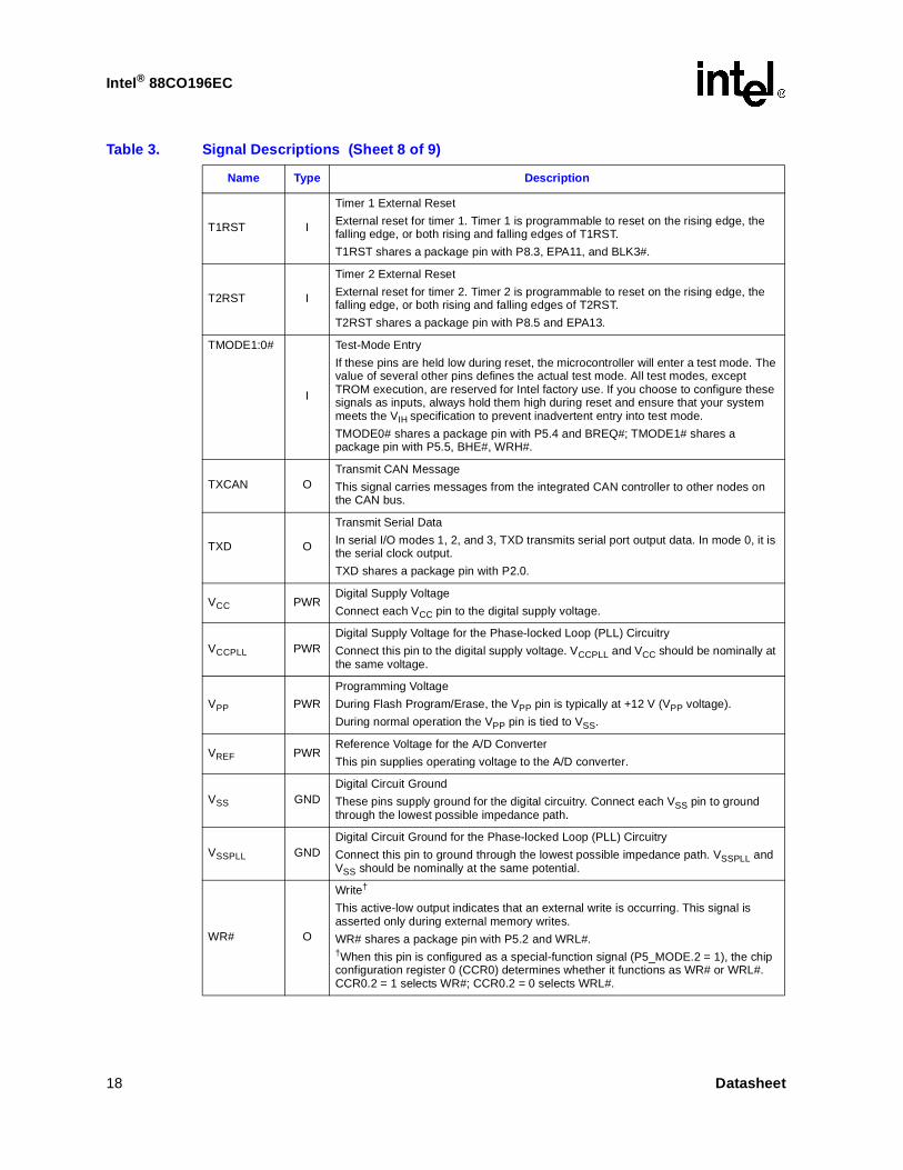
T1RST I
Timer 1 External Reset
External reset for timer 1. Timer 1 is programmable to reset on the rising edge, the falling edge, or both rising and falling edges of T1RST.
T1RST shares a package pin with P8.3, EPA11, and BLK3#.
T2RST I
Timer 2 External Reset
External reset for timer 2. Timer 2 is programmable to reset on the rising edge, the falling edge, or both rising and falling edges of T2RST.
T2RST shares a package pin with P8.5 and EPA13.
TMODE1:0#
I
Test-Mode Entry
If these pins are held low during reset, the microcontroller will enter a test mode. The value of several other pins defines the actual test mode. All test modes, except TROM execution, are reserved for Intel factory use. If you choose to configure these signals as inputs, always hold them high during reset and ensure that your system meets the VIH specification to prevent inadvertent entry into test mode.
TMODE0# shares a package pin with P5.4 and BREQ#; TMODE1# shares a package pin with P5.5, BHE#, WRH#.
TXCAN OTransmit CAN Message
This signal carries messages from the integrated CAN controller to other nodes on the CAN bus.
TXD O
Transmit Serial Data
In serial I/O modes 1, 2, and 3, TXD transmits serial port output data. In mode 0, it is the serial clock output.
TXD shares a package pin with P2.0.
VCC PWRDigital Supply Voltage
Connect each VCC pin to the digital supply voltage.
VCCPLL PWRDigital Supply Voltage for the Phase-locked Loop (PLL) Circuitry
Connect this pin to the digital supply voltage. VCCPLL and VCC should be nominally at the same voltage.
VPP PWR
Programming Voltage
During Flash Program/Erase, the VPP pin is typically at +12 V (VPP voltage).
During normal operation the VPP pin is tied to VSS.
VREF PWRReference Voltage for the A/D Converter
This pin supplies operating voltage to the A/D converter.
VSS GNDDigital Circuit Ground
These pins supply ground for the digital circuitry. Connect each VSS pin to ground through the lowest possible impedance path.
VSSPLL GNDDigital Circuit Ground for the Phase-locked Loop (PLL) Circuitry
Connect this pin to ground through the lowest possible impedance path. VSSPLL and VSS should be nominally at the same potential.
WR# O
Write†
This active-low output indicates that an external write is occurring. This signal is asserted only during external memory writes.
WR# shares a package pin with P5.2 and WRL#.†When this pin is configured as a special-function signal (P5_MODE.2 = 1), the chip configuration register 0 (CCR0) determines whether it functions as WR# or WRL#. CCR0.2 = 1 selects WR#; CCR0.2 = 0 selects WRL#.
Table 3. Signal Descriptions (Sheet 8 of 9)
Name Type Description

Intel® 88CO196EC
Datasheet 19
WRH# O
Write High†
During 16-bit bus cycles, this active-low output signal is asserted for high-byte writes and word writes to external memory. During 8-bit bus cycles, WRH# is asserted for all write operations.
WRH# shares a package pin with P5.5 and BHE#.
† When this pin is configured as a special-function signal (P5_MODE.5 = 1), the chip configuration register 0 (CCR0) determines whether it functions as BHE# or WRH#. CCR0.2 = 1 selects BHE#; CCR0.2 = 0 selects WRH#.
WRL# O
Write Low†
During 16-bit bus cycles, this active-low output signal is asserted for low-byte writes and word writes to external memory. During 8-bit bus cycles, WRL# is asserted for all write operations.
WRL# shares a package pin with P5.2 and WR#.†When this pin is configured as a special-function signal (P5_MODE.2 = 1), the chip configuration register 0 (CCR0) determines whether it functions as WR# or WRL#. CCR0.2 = 1 selects WR#; CCR0.2 = 0 selects WRL#.
XTAL1 I
Input Crystal/Resonator or External Clock Input
Input to the on-chip oscillator and the internal clock generators. The internal clock generators provide the peripheral clocks, CPU clock, and CLKOUT signal. When using an external clock source instead of the on-chip oscillator, connect the clock input to XTAL1. The external clock signal must meet the VIH specification for XTAL1.
XTAL2 OInverted Output for the Crystal/Resonator
Output of the on-chip oscillator inverter. Leave XTAL2 floating when the design uses an external clock source instead of the on-chip oscillator.
Table 3. Signal Descriptions (Sheet 9 of 9)
Name Type Description

Intel® 88CO196EC
20 Datasheet

Intel® 88CO196EC
Datasheet 21
4.0 Address Map
Table 4. Intel® 88CO196EC CHMOS 16-Bit Microcontroller Address Map (Sheet 1 of 2)
Hex Address Description Addressing Modes
for Data Accesses
FFFFFF
FF2140Internal flash program memory or external program memory (Notes 1 and 2) Extended
FF213F
FF20C0Internal flash special-purpose memory or external special-purpose memory (PIH vectors) (Notes 1 and 2) Extended
FF20BF
FF2080Internal flash program memory or external program memory (Notes 1 and 2). After reset, the first instruction is fetched from FF2080H. Extended
FF207F
FF2000Internal flash special-purpose memory or external special-purpose memory (CCBs, interrupt vectors, and PTS vectors) (Notes 1 and 2) Extended
FF1FFF
FC0000Internal flash program memory or external program memory (Notes 1 and 2) Extended
FBFFFF
FB0000External memory or I/O (Note 1) Extended
FAFFFF
E10000External memory or I/O Extended
E0FFFF
010000Reserved for future microcontrollers, do not access these locations. (Note 3) —
00FFFF
002000External memory or I/O Indirect, indexed,
extended
001FFF
001FE0Memory-mapped special-function registers (SFRs) Indirect, indexed,
extended
001FDF
001E00Peripheral special-function registers (SFRs)
Indirect, indexed, extended, windowed direct
001DFF
001D00CAN special-function registers (SFRs)
Indirect, indexed, extended, windowed direct
001CFF
001C00Upper register file (general-purpose register RAM)
Indirect, indexed, extended, windowed direct
001BFF
000F00External memory or I/O Indirect, indexed,
extended
NOTES:1. During test ROM execution mode, the contents of pages FFH and FBH are swapped. This allows the
microcontroller to enter a test ROM routine after reset.2. Accesses to these locations go to internal flash if EA# is high or an external device if EA# is low.3. Since the upper three address bits, A23:21, are not connected to external pins, these address locations are
unique internally, but not externally. For example, addresses 200F20H, 400F20H, 600F20H appear externally on address pins A20:0 as 000F20H.
4. The IRAM_CON register determines whether accesses to these locations go to internal code/data RAM or external memory. Accesses to these locations go internal if IRAM_CON.6 = 0 and external if IRAM_CON.6 = 1.

Intel® 88CO196EC
22 Datasheet
000EFF
000400Internal code/data RAM or external memory (Note 4) Indirect, indexed,
extended
0003FF
000100Upper register file (general-purpose register RAM)
Indirect, indexed, extended, windowed direct
0000FF
000018Lower register file (general-purpose register RAM) Direct, indirect,
indexed, extended
000017
000000Lower register file (stack pointer and CPU SFRs) Direct, indirect,
indexed, extended
Table 4. Intel® 88CO196EC CHMOS 16-Bit Microcontroller Address Map (Sheet 2 of 2)
Hex Address Description Addressing Modes
for Data Accesses
NOTES:1. During test ROM execution mode, the contents of pages FFH and FBH are swapped. This allows the
microcontroller to enter a test ROM routine after reset.2. Accesses to these locations go to internal flash if EA# is high or an external device if EA# is low.3. Since the upper three address bits, A23:21, are not connected to external pins, these address locations are
unique internally, but not externally. For example, addresses 200F20H, 400F20H, 600F20H appear externally on address pins A20:0 as 000F20H.
4. The IRAM_CON register determines whether accesses to these locations go to internal code/data RAM or external memory. Accesses to these locations go internal if IRAM_CON.6 = 0 and external if IRAM_CON.6 = 1.

Intel® 88CO196EC
Datasheet 23
5.0 Electrical Characteristics
5.1 DC Characteristics
ABSOLUTE MAXIMUM RATINGS†
Storage Temperature ....................................... –60°C to +150°C
VCC Supply Voltage with Respect to VSS .......... –0.5 V to +6.0 V
VPP (maximum) ..................................................................13.0 V
Power Dissipation............................................................... 1.5 W
OPERATING CONDITIONS†
TC (Case Temperature Under Bias) (note 4) ................................Extended Temperature............. –40°C to +85°CCommercial Temperature......... 0°C to +70°C
VCC (Digital Supply Voltage) ............................. 4.75 V to 5.25 V
VPP (normal operation).................................................. tie to VSS
VPP (Flash program/erase)..................................11.4 V to 12.6 V
VREF (Analog Supply Voltage) .......................... 4.75 V to 5.25 V
FXTAL1 (Input frequency for VCC = 4.75 V – 5.25 V) (Notes 1, 2, 3).................................................. 16MHz to 40MHz
NOTICE: This datasheet contains information on products being sampled or in the initial production phase of development. The specifications are subject to change without notice. Verify with your local Intel sales office that you have the latest datasheet before finalizing a design.
†WARNING: Stressing the device beyond the “Absolute Maximum Ratings” may cause permanent damage. These are stress ratings only. Operation beyond the “Operating Conditions” is not recommended and extended exposure beyond the “Operating Conditions” may affect device reliability.
NOTE:1. This device is static and should operate below 1 Hz, but has been tested only down to 16 MHz.2. When the phase-locked loop (PLL) circuitry is enabled, the minimum input frequency on XTAL1 is 6 MHz.
The PLL cannot be run at frequencies lower than 24 MHz in 4X mode.3. Assume an external clock. The maximum frequency for an external crystal oscillator is 20MHz.4. Flash programming and erase operations only guaranteed to work from 0°C to +70°C.
Table 5. DC Characteristics at VCC = 4.75 V – 5.25 V (Sheet 1 of 2)
Sym Parameter Min Typical (Note 1) Max Units Test Conditions
ICCVCC supply current
40MHz100 130 mA
VCC = 5.25 V
Device in Reset
IIDLEIdle mode current
40MHz60 85 mA VCC = 5.25 V
IPDPowerdown mode current 50 µA VCC = 5.25 V
NOTES:1. Typical values are based on a limited number of samples and are not guaranteed. The values listed are at
room temperature with VCC = 5.0 V.2. For P2.7:0, P3.7:0, P4.7:0, P5.7:0, P6.7:0, P7.7:0, P8.7:0, P9.7:0, RESET#, NMI, CRIN, CRDCLK, ONCE#,
and XTAL1.3. The maximum injection current is not tested. The device is designed to meet this specification.4. Pin capacitance is not tested. This value is based on design simulations.

Intel® 88CO196EC
24 Datasheet
IREFA/D reference supply current 6 mA
XTAL1 = 40 MHz
VCC = VREF = 5.25 V
Device in Reset
IINJD
Maximum injection current per port on bidirectional pins (Note 3)
–10 10 mA
ILI
Input leakage current (Standard inputs except analog inputs)
–10 10 µA VSS < VIN < VCC
ILI1Input leakage current (analog inputs) –300 300 nA VSS + 100 mV < VIN < VREF – 100 mV
IIHInput high current(NMI only) 175 µA NMI = VCC = 5.25 V
VIL1Input low voltage (Note 2) –0.5 0.3 VCC V
VIH1Input high voltage (Note 2) 0.7 VCC
VCC + 0.5 V
VOL1
Output low voltage (output configured as complementary)
0.3
0.45
1.5
V
V
V
IOL = 200 µA
IOL = 3.2 mA
IOL = 7 mA
VOH1
Output high voltage (output configured as complementary)
VCC – 0.3
VCC – 0.7
VCC – 1.5
V
V
V
IOH = –200 µA
IOH = –3.2 mA
IOH = –7 mA
IOH2
Output high current in reset (on any pin except ONCE# and TMODEx#)
–30
–65
–75
–140
–280
–350
µA
µA
µA
VOH2 = VCC – 1 V
VOH2 = VCC – 2.5 V
VOH2 = VCC – 4 V
VOL2Output low voltage in reset (on ALE) 0.5 V IOL = 15 µA
VHYSHysteresis voltage on RESET# 700 mV
CSPin Capacitance (any pin to VSS) (Note 4) 10 pF Not tested
RRSTPull-up resistor on RESET# pin 9 95 kΩ
VCC = 5.25 V
VIN = 4 V
Ipph VPP Current during erase/write operation 40 mA
Table 5. DC Characteristics at VCC = 4.75 V – 5.25 V (Sheet 2 of 2)
Sym Parameter Min Typical (Note 1) Max Units Test Conditions
NOTES:1. Typical values are based on a limited number of samples and are not guaranteed. The values listed are at
room temperature with VCC = 5.0 V.2. For P2.7:0, P3.7:0, P4.7:0, P5.7:0, P6.7:0, P7.7:0, P8.7:0, P9.7:0, RESET#, NMI, CRIN, CRDCLK, ONCE#,
and XTAL1.3. The maximum injection current is not tested. The device is designed to meet this specification.4. Pin capacitance is not tested. This value is based on design simulations.

Intel® 88CO196EC
Datasheet 25
6.0 Explanation of AC Symbols
Table 6. AC Timing Symbol Definitions
Character Signal(s)
A AD15:0, A20:0
BR BREQ#
C CLKOUT
D AD15:0, AD7:0, RXD (SIO mode 0 input data), SDx (SSIO input data)
H CRBUSY#
L ALE/ADV#
Q AD15:0, AD7:0, RXD (SIO mode 0 output data), SDx (SSIO output data)
R RD#
S CSx#
W WR#, WRH#, WRL#
X XTAL1, TXD (SIO clock), SCx (SSIO standard mode clock)
Y READY
Character Condition
H High
L Low
V Valid
X No Longer Valid
Z Floating (low impedance)

Intel® 88CO196EC
26 Datasheet
6.1 AC Characteristics — Multiplexed Bus Mode
Test Conditions: Capacitive load on all pins = 50 pF, Rise and Fall Times = 3 ns.
Table 7. AC Characteristics, Multiplexed Bus Mode (Sheet 1 of 2)
Symbol Parameter Min Max Units
FXTAL1
Frequency on XTAL1, PLL in 1x mode (disabled) 16 40 MHz (1, 2)
Frequency on XTAL1, PLL in 4x mode 6 10 MHz
f Operating frequency, f = FXTAL1; PLL in 1x mode (disabled) 16 40 MHz
Operating frequency, f = 4FXTAL1; PLL in 4x mode 24 40 MHz
t Period, t = 1/f; 25 62.5 ns
TAVDV Address Valid to Input Data Valid 3t – 40 ns (3)
TRLDV RD# Low to Input Data Valid t – 30 ns (3)
TCHDV CLKOUT High to Input Data valid 2t – 35 ns (4)
TRHDZ RD# High to Input Data Float t + 3 ns
TRXDX Data Hold after RD# Inactive 0 ns
TXHCH XTAL1 Rising Edge to CLKOUT High or Low 3 50 ns (4)
TCLCL CLKOUT Cycle Time 2t ns (4)
TCHCL CLKOUT High Period t – 10 t + 15 ns (4)
TCLLH CLKOUT Low to ALE High – 10 10 ns (4)
TLLCH ALE Low to CLKOUT High – 15 15 ns (4)
TLHLH ALE Cycle Time 4t ns (3)
TLHLL ALE High Period t – 10 t + 10 ns
TAVLL Address Setup to ALE Low t – 15 ns
TLLAX Address Hold after ALE Low t – 10 ns
TLLRL ALE Low to RD# Low t – 15 ns
TRLCL RD# Low to CLKOUT Low – 10 20 ns (4)
TRLRH RD# Low to RD# High t – 10 ns (3)
TRHLH RD# High to ALE High t – 5 t + 15 ns (5)
TRLAZ RD# Low to Address Float 5 ns
TLLWL ALE Low to WR# Low t – 12 ns
TQVWH Output Data Stable to WR# High t – 14 ns (3)
TCHWH CLKOUT High to WR# High – 15 6.5 ns (4)
NOTES:1. 20MHz is the maximum input frequency when using an external crystal oscillator; however, 40MHz can be
applied with an external clock source.2. Device is static by design, but has been tested only down to 16MHz.3. If wait states are used, add 2t × n, where n = number of wait states.4. Assumes CLKOUT is operating in divide-by-two mode (f/2).5. Assuming back-to-back bus cycles.6. 8-bit bus only.7. When forcing wait states using the BUSCONx register, add 2t × n, where n = number of wait states.8. Exceeding the maximum specification causes additional wait states.9. The first falling edge of READY is not synchronized to a CLKOUT edge; therefore, one programmed wait
state is required.

Intel® 88CO196EC
Datasheet 27
TWLWH WR# Low to WR# High t – 10 ns (3)
TWHQX Output Data Hold after WR# High 40 MHz = t-13 t – 13 ns
TWHLH WR# High to ALE High t – 15 t + 20 ns
TWHBX BHE#, INST Hold after WR# High t – 4 ns
TWHAX AD15:8, CSx# Hold after WR# High 40 MHz = t-9 t – 9 ns (6)
TRHBX BHE#, INST Hold after RD# High t – 5 ns (6)
TRHAX AD15:8, CSx# Hold after RD# High t – 5 ns (6)
TWHSH A20:0, CSx# Hold after WR# High – 0.5 ns
TRHSH A20:0, CSx# Hold after RD# High 0 ns
TAVYV AD15:0 Valid to READY Setup 2t – 55 ns (7)
TCLYX READY Hold after CLKOUT Low 0 2t – 45 ns (4,8,9)
TYLYH READY Low to READY High No Upper Limit ns
Table 7. AC Characteristics, Multiplexed Bus Mode (Sheet 2 of 2)
Symbol Parameter Min Max Units
NOTES:1. 20MHz is the maximum input frequency when using an external crystal oscillator; however, 40MHz can be
applied with an external clock source.2. Device is static by design, but has been tested only down to 16MHz.3. If wait states are used, add 2t × n, where n = number of wait states.4. Assumes CLKOUT is operating in divide-by-two mode (f/2).5. Assuming back-to-back bus cycles.6. 8-bit bus only.7. When forcing wait states using the BUSCONx register, add 2t × n, where n = number of wait states.8. Exceeding the maximum specification causes additional wait states.9. The first falling edge of READY is not synchronized to a CLKOUT edge; therefore, one programmed wait
state is required.

Intel® 88CO196EC
28 Datasheet
Figure 4. System Bus Timing Diagram (Multiplexed Bus Mode)
CLKOUT
ALE
RD#
A3252-01
AD15:0(read)
WR#
AD15:0(write)
BHE#, INST
AD15:8
A20:16
TLHLH
Address Out
Extended Address Out
tTCLLH
TCLCL
TCHDVTRLCL TCHCL
TLLCH
TLLRL
TRHLH
TRLRH
TRLDV
TRHDZ
Data In
TRLAZ
TLLAX
Address Out
TAVDV
TAVLL
TCHWHTWHLHTLLWL
TWLWH TWHQX
Data OutAddress Out
TWLWH
TQVWH
TWHBX, TRHBX
High Address Out
TWHSH, TRHSH
CSx#
TWHAX, TRHAX
TLHLL

Intel® 88CO196EC
Datasheet 29
Figure 5. READY Timing Diagram (Multiplexed Bus Mode)
CLKOUT
READY
ALE
A3249-01
TCLYX (min)
TLHLH + 2t
TAVDV + 2t
RD#
AD15:0(read)
AD15:0(write)
BHE#, INST
A20:16
CSx#
TRLRH + 2t
TAVYV
Data Out
Extended Address Out
Address Out
TCLYX (max)
Data InAddress Out
TRLDV + 2t
TWLWH + 2t
TQVWH + 2t
WR#

Intel® 88CO196EC
30 Datasheet
6.2 AC Characteristics — Demultiplexed Bus Mode
Test Conditions: Capacitive load on all pins = 50 pF, Rise and Fall Times = 3 ns.
Table 8. AC Characteristics, Demultiplexed Bus Mode (Sheet 1 of 2)
Symbol Parameter Min Max Units
FXTAL1
Frequency on XTAL1, PLL in 1x mode (disabled) 16 40 MHz (1,2)
Frequency on XTAL1, PLL in 4x mode 6 10 MHz
f Operating frequency, f = FXTAL1; PLL in 1x mode (disabled) 16 40 MHz
Operating frequency, f = 2FXTAL1; PLL in 4x mode 24 40 MHz
t Period, t = 1/f 25 62.5 ns
TAVDV Address Valid to Input Data Valid 4t –40 ns (3)
TRLDV RD# Low to Input Data Valid 3t – 35 ns (3)
TAVWL Address Valid to WR# Low t ns
TAVRL Address Valid to RD# Low t – 8 ns
TSLDV CSx# Low to Data Valid 4t – 40 ns (3)
TCHDV CLKOUT High to Input Data Valid 2t – 35 ns (4)
TRHRL Read High to Read Low t – 5 ns
TRXDX Data Hold after RD# Inactive 0 ns
TXHCH XTAL1 High to CLKOUT High or Low 3 50 ns (4)
TCLCL CLKOUT Cycle Time 2t ns (4)
TCHCL CLKOUT High Period t – 10 t + 15 ns (4)
TCLLH CLKOUT High ALE Low – 10 10 ns (4)
TLLCH ALE High to CLKOUT Low – 15 15 ns (4)
TLHLH ALE Cycle Time 4t ns (3,5)
TLHLL ALE High Period t – 10 t + 10 ns
TRLCL RD# Low to CLKOUT Low – 15 5 ns (4)
TRLRH RD# Low to RD# High 3t – 18 ns (3)
TRHLH RD# High to ALE Low t – 4 t + 15 ns (5)
TWLCL WR# Low to CLKOUT Low – 15 5 ns (4)
TQVWH Output Data Stable to WR# High 3t – 25 ns (5)
TCHWH CLKOUT High to WR# High – 11 10 ns (4)
1. Device is static by design but has been tested only down to 16MHz.2. 20MHz is the maximum input frequency when using an external crystal oscillator; however, 40MHz can be
applied with an external clock source.3. If wait states are used, add 2t × n, where n = number of wait states.4. Assumes CLKOUT is operating in divide-by-two mode (f/2).5. Assuming back-to-back bus cycles.6. When forcing wait states using the BUSCON register, add 2t × n.7. Exceeding the maximum specification causes additional wait states.8. The first falling edge of READY is not synchronized to a CLKOUT edge; therefore, one programmed wait
state is required.9. 8-bit bus only.

Intel® 88CO196EC
Datasheet 31
TWLWH WR# Low to WR# High 3t – 18 ns (3)
TWHQX Output Data Hold after WR# High t – 2 t + 20 ns
TWHLH WR# High to ALE High t – 5 t + 10 ns (3)
TWHBX BHE#, INST Hold after WR# High t – 5 ns
TWHAX A20:0, CSx# Hold after WR# High 0 ns
TRHBX BHE#, INST Hold after RD# High t – 5 ns
TRHAX A20:0, CSx# Hold after RD# High 0 ns
TAVYV A20:0 Valid to READY Setup 3t – 45 ns (6)
TCLYX READY Hold after CLKOUT Low 0 2t – 36 ns (7,8,9)
TYLYH READY Low to READY High No Upper Limit ns
Table 8. AC Characteristics, Demultiplexed Bus Mode (Sheet 2 of 2)
Symbol Parameter Min Max Units
1. Device is static by design but has been tested only down to 16MHz.2. 20MHz is the maximum input frequency when using an external crystal oscillator; however, 40MHz can be
applied with an external clock source.3. If wait states are used, add 2t × n, where n = number of wait states.4. Assumes CLKOUT is operating in divide-by-two mode (f/2).5. Assuming back-to-back bus cycles.6. When forcing wait states using the BUSCON register, add 2t × n.7. Exceeding the maximum specification causes additional wait states.8. The first falling edge of READY is not synchronized to a CLKOUT edge; therefore, one programmed wait
state is required.9. 8-bit bus only.

Intel® 88CO196EC
32 Datasheet
Figure 6. System Bus Timing Diagram (Demultiplexed Bus Mode)
A8733-01
CLKOUT
ALE
RD#
AD15:0(read)
WR#
AD15:0(write)
BHE#, INST
A20:0 Address Out
TCHCL TCLCL
TLLCH
TCHWH
TLHLHTWHLH
TRHRL
Data In
TRLRH
TAVDV
TWHQXTWHAX
TWLCL
Data Out
TWLWH
TQVWH
TWHBX, TRHBX
CSx#
TLHLL
TCLLH
t
TRHLH
TAVRLTRHAX
TSLDV
TCHDVTRLDV
TAVWL

Intel® 88CO196EC
Datasheet 33
Figure 7. READY Timing Diagram (Demultiplexed Bus Mode)
CLKOUT
READY
ALE
A3259-02
TLHLH + 2t
TAVDV + 2t
RD#
AD15:0(read)
AD15:0(write)
BHE#, INST
A20:0
CSx#
TRLRH + 2t
TAVYV
Data Out
Address Out
Data In
TRLDV + 2t
TWLWH + 2t
TQVWH + 2t
WR#
TCLYX (max)
TCLYX (min)

Intel® 88CO196EC
34 Datasheet
6.3 Deferred Bus Timing Mode
The deferred bus cycle mode (enabled by setting CCR1.5) reduces bus contention when using the Intel® 88CO196EC in demultiplexed mode with slow memories. As shown in Figure 8, a delay of 2t occurs in the first bus cycle following a chip-select output change or the first write cycle following a read cycle.
Figure 8. Deferred Bus Mode Timing Diagram
CLKOUT
ALE
RD#
A3246-02
TWHLH + 2t
TRHLH + 2tTAVRL + 2t
TAVWL + 2tAD15:0
(read)
WR#
AD15:0(write)
BHE#, INST
A20:0
CSx#
TAVDV+ 2t
TLHLH + 2t
Data InData In
Data Out
Valid Valid
Data Out
Address Out
Data Out

Intel® 88CO196EC
Datasheet 35
6.4 AC Characteristics — Serial Port, Mode 0
Table 9. Serial Port Timing — Mode 0†
Symbol Parameter Min Max Units
TXLXL
Serial Port Clock period
SP_BAUD ≥ x002HSP_BAUD = x001H††
6t4t
nsns
TXLXH
Serial Port Clock falling edge to rising edge
SP_BAUD ≥ x002HSP_BAUD = x001H††
4t – 272t – 27
4t + 272t + 27
nsns
TQVXH Output data setup to clock high 4t – 30 ns
TXHQX Output data hold after clock high 2t – 30 ns
TXHQV Next output data valid after clock high 2t + 30 ns
TDVXH Input data setup to clock high 2t + 30 ns
TXHDX Input data hold after clock high 0 ns
TXHQZ Last clock high to output float t + 30 ns
† These timings are not tested and not guaranteed.
†† The minimum baud-rate (SP_BAUD) register value for receptions is x002H and the minimum baud-rate (SP_BAUD) register value for transmissions is x001H.
Figure 9. Serial Port Waveform — Mode
A5013-01
Valid Valid Valid Valid Valid Valid Valid ValidRXD
TXD
0 1 2 3 4 5 6 7
TQVXH
TXLXL
TDVXH
TXHQVTXHQZ
TXHDX
TXHQXTXLXH
RXD

Intel® 88CO196EC
36 Datasheet
6.5 AC Characteristics — Synchronous Serial Port
Table 10. Synchronous Serial Port Timing
Symbol Parameter Min Max Units
TCLCL Synchronous Serial Port Clock period 4t ns
TCLCH Synchronous Serial Port Clock falling edge to rising edge 2t – 10 ns
TD1DV Setup time for MSB output† t ns
TCLDX Output data change after clock low 0.5t 1.5t + 20 ns
TDVCX Setup time for input data 10 ns
TDXCX Input data hold after clock high t + 5 ns
† Refer to the “Programming Considerations” section of chapter 9, “Synchronous Serial I/O Port” in the Intel® 88CO196EC CHMOS 16-Bit Microcontroller196EC User’s Manual.
Figure 10. Synchronous Serial Port
MSB D6 D5 D4 D3 D2 D1 D0
valid valid valid valid valid valid valid valid
1 8765432
1 8765432
SCx(normal
transfers)
SDx (out)
SDx (in)
SCx(handshaking
transfers) Slave Receiver Pulls SCx low
A3233-02
TCHCH
TCHCLTCLCH
STE Bit
TD1DV
TCXDX TCXDV
TDVCX TDXCX
Assumes that the SSIO is configured to sample incoming data on the rising clock edge and sample outgoingdata on the falling clock edge, and that the SSIO is configured to pull the clock signal low while the channelis idle.
†
†

Intel® 88CO196EC
Datasheet 37
6.6 AC Characteristics — Serial Debug Unit
Table 11. Serial Debug Unit Timing
Symbol Parameter Min Max Units
TCLCL Code RAM clock cycle time 2t ns
TCHCL Code RAM clock high period t ns
TDVCH Input data setup to clock high 10 ns
TCHDX Input data hold after clock high t + 10 ns
TQVCH Output data setup to clock high t – 10 ns
TCHQX Output data hold after clock high t – 10 ns
TCHQV Next output data valid after clock high t + 10 ns
TCHHL Last clock high to CRBUSY# low 3t + 20 ns
Figure 11. Serial Debug Unit
TCHHL
CRDCLK
CRIN
CROUT
CRBUSY#
A5335-01
TCLCL
validvalidvalid
TCHCL
TDVCH TCHDX
TCHQX
TCHQVTQVCH
Intel® 88CO196EC
38 Datasheet
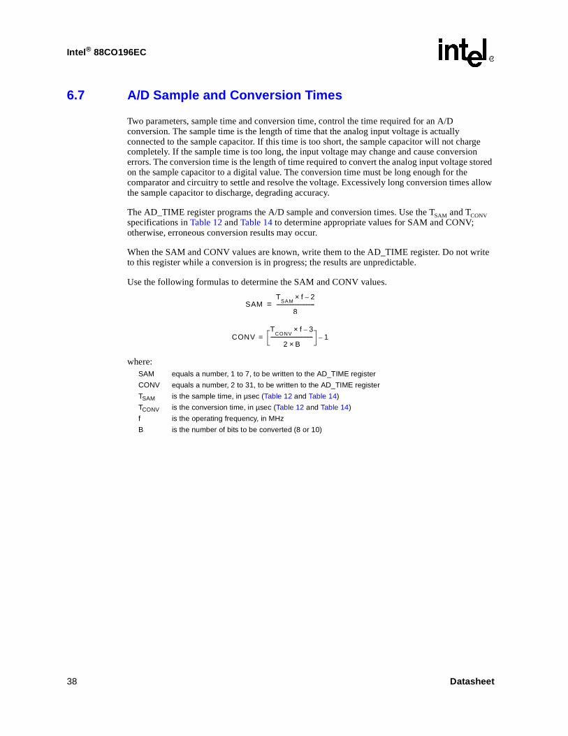
6.7 A/D Sample and Conversion Times
Two parameters, sample time and conversion time, control the time required for an A/D conversion. The sample time is the length of time that the analog input voltage is actually connected to the sample capacitor. If this time is too short, the sample capacitor will not charge completely. If the sample time is too long, the input voltage may change and cause conversion errors. The conversion time is the length of time required to convert the analog input voltage stored on the sample capacitor to a digital value. The conversion time must be long enough for the comparator and circuitry to settle and resolve the voltage. Excessively long conversion times allow the sample capacitor to discharge, degrading accuracy.
The AD_TIME register programs the A/D sample and conversion times. Use the TSAM and TCONV specifications in Table 12 and Table 14 to determine appropriate values for SAM and CONV; otherwise, erroneous conversion results may occur.
When the SAM and CONV values are known, write them to the AD_TIME register. Do not write to this register while a conversion is in progress; the results are unpredictable.
Use the following formulas to determine the SAM and CONV values.
where:SAM equals a number, 1 to 7, to be written to the AD_TIME register
CONV equals a number, 2 to 31, to be written to the AD_TIME register
TSAM is the sample time, in µsec (Table 12 and Table 14)
TCONV is the conversion time, in µsec (Table 12 and Table 14)
f is the operating frequency, in MHz
B is the number of bits to be converted (8 or 10)
SAMT
SAMf 2–×
8-------------------------------=
CONVT
CONVf× 3–
2 B×---------------------------------- 1–=

Intel® 88CO196EC
Datasheet 39
6.7.1 AC Characteristics — A/D Converter, 10-Bit Mode
Table 12. 10-bit A/D Operating Conditions
Symbol Description Min Max Units Notes
1
TC Case Temperature – 40 + 125 °C
VCC Digital Supply Voltage 4.75 5.25 V
VREF Analog Supply Voltage 4.75 5.25 V 2
TSAM Sample Time 1.0 µs 3
TCONV Conversion Time 10.0 15.0 µs 3
NOTES:1. ANGND and VSS should nominally be at the same potential.2. VREF must not exceed VCC by more than + 0.5 V because VREF supplies both the resistor ladder and the
analog portion of the converter and input port pins.3. Program the AD_TIME register to meet the TSAM and TCONV specifications.
Table 13. 10-Bit Mode A/D Characteristics Over Specified Operating Conditions
Parameter Typical (2) Min Max Units (3) Notes
1
Resolution1024
10
1024
10
Levels
Bits
Absolute Error 0 ± 3.0 LSBs
Full-scale Error 0.25 ± 0.5 LSBs
Zero Offset Error 0.25 ± 0.5 LSBs
Nonlinearity 1.0 ± 2.0 ± 3.0 LSBs
Differential Nonlinearity – 0.75 + 0.75 LSBs
Channel-to-channel Matching ± 0.1 0 ± 1.0 LSBs
Repeatability ± 0.25 0 LSBs
Temperature Coefficients:
Offset
Full-scale
Differential Nonlinearity
0.009
0.009
0.009
LSB/°C
LSB/°C
LSB/°C
Off-isolation – 60 dB 2, 4, 5
Feedthrough – 60 dB 2, 4
VCC Power Supply Rejection – 60 dB 2, 4
Input Series Resistance 750 1.2k W 6
Voltage on Analog Input Pin ANGND VREF V 7
Sampling Capacitor 3.0 pF
DC Input Leakage ± 100 0 ± 300 nA 8
NOTES:1. All conversions were performed with processor in idle mode.2. Most devices will need these values at 25°C, but they are not tested or guaranteed.3. An LSB, as used here, has a value of approximately 5 mV. 4. DC to 100 KHz.5. Multiplexer break-before-make guaranteed.6. Resistance from device pin, through internal multiplexer, to sample capacitor.7. Applying voltage beyond these specifications will degrade the accuracy of other channels being converted.8. 100 mV < VIN < VREF – 100 mV.

Intel® 88CO196EC
40 Datasheet
6.7.2 AC Characteristics — A/D Converter, 8-Bit Mode
Table 14. 8-Bit A/D Operating Conditions
Symbol Description Min Max Units Notes
1
TC Case Temperature – 40 + 125 °C
vCC Digital Supply Voltage 4.75 5.25 V
vREF Analog Supply Voltage 4.75 5.25 V 2
TSAM Sample Time 1.0 µs 3
TCONV Conversion Time 8.0 12.8 µs 3
NOTES:1. ANGND and VSS should nominally be at the same potential.2. VREF must not exceed VCC by more than + 0.5 V because VREF supplies both the resistor ladder and the
analog portion of the converter and input port pins.3. Program the AD_TIME register to meet the TSAM and TCONV specifications.
Table 15. 8-Bit Mode A/D Characteristics Over Specified Operating Conditions
Parameter Typical (2) Min Max Units (3) Notes
1
Resolution256
8
256
8
Levels
Bits
Absolute Error 0 ± 1.0 LSBs
Full-scale Error ± 0.5 LSBs
Zero Offset Error ± 0.5 LSBs
Nonlinearity 0 ± 1.0 LSBs
Differential Nonlinearity – 0.5 + 0.5 LSBs
Channel-to-channel Matching 0 ± 1.0 LSBs
Repeatability ± 0.25 0 LSBs
Temperature Coefficients:
Offset
Full-scale
Differential Nonlinearity
0.003
0.003
0.003
LSB/°C
LSB/°C
LSB/°C
Off Isolation – 60 dB 2, 4, 5
Feedthrough – 60 dB 2, 4
VCC Power Supply Rejection – 60 dB 2, 4
Input Series Resistance 750 1.2K Ω 6
Voltage on Analog Input Pin ANGND VREF V 7
Sampling Capacitor 3.0 pF
DC Input Leakage 100 0 300 nA 8
NOTES:1. All conversions were performed with processor in idle mode.2. Most parts will need these values at 25°C, but they are not tested or guaranteed.3. An LSB, as used here, has a value of approximately 5 mV.4. DC to 100 KHz.5. Multiplexer break-before-make guaranteed.6. Resistance from device pin, through internal multiplexer, to sample capacitor.7. Applying voltage beyond these specifications will degrade the accuracy of other channels being converted.8. 100 mV < VIN < VREF – 100 mV.
Intel® 88CO196EC
Datasheet 41
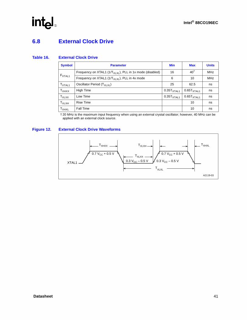
6.8 External Clock Drive
Table 16. External Clock Drive
Symbol Parameter Min Max Units
FXTAL1
Frequency on XTAL1 (1/TXLXL), PLL in 1x mode (disabled) 16 40† MHz
Frequency on XTAL1 (1/TXLXL), PLL in 4x mode 6 10 MHz
TXTAL1 Oscillator Period (TXLXL) 25 62.5 ns
TXHXX High Time 0.35TXTAL1 0.65TXTAL1 ns
TXLXX Low Time 0.35TXTAL1 0.65TXTAL1 ns
TXLXH Rise Time 10 ns
TXHXL Fall Time 10 ns
† 20 MHz is the maximum input frequency when using an external crystal oscillator; however, 40 MHz can be applied with an external clock source.
Figure 12. External Clock Drive Waveforms
TXLXX
A2119-03
TXHXX TXHXL
TXLXL
0.3 VCC – 0.5 V
0.7 VCC + 0.5 V
TXLXH
0.7 VCC + 0.5 V
0.3 VCC – 0.5 VXTAL1

Intel® 88CO196EC
42 Datasheet
6.9 Test Output Waveforms
6.10 Flash Memory Erase Performance
Figure 13. AC Testing Output Waveforms
Figure 14. Float Waveforms During 5.0 Volt Testing
Table 17. Flash Memory Erase Performance
Parameter Note Min Typical(see note) Max Unit
Flash erase time 2 10 Sec.
NOTE: Typical values are based on limited number of samples and are not guaranteed. The values listed are at room temperature with VCC = 5 V; VPP= 12 V.
Test Points2.0 V
0.8 V
Note:AC testing inputs are driven at 3.5 V for a logic “ 1” and 0.45 V for a logic“ 0” . Timing measurements are made at 2.0 V for a logic “ 1” and 0.8 V fora logic “ 0”.
3.5 V
0.45 V
A2120-04
2.0 V
0.8 V
VLOAD
VLOAD – 0.15 V
VLOAD + 0.15 VTiming Reference
Points
VOH – 0.15 V
VOL + 0.15 V
Note:For timing purposes, a port pin is no longer floating when a 150 mV change from loadvoltage occurs and begins to float when a 150 mV change from the loading VOH/VOLlevel occurs with IOL/IOH ≤ 15 mA.
A2121-03

Intel® 88CO196EC
Datasheet 43
7.0 Thermal Characteristics
All thermal impedance data is approximate for static air conditions at 1 watt of power dissipation. Values will change depending on operating conditions and the application. The Intel Packaging Handbook (order number 240800) describes Intel’s thermal impedance test methodology. The Components Quality and Reliability Handbook (order number 210997) provides quality and reliability information.
Table 18. Thermal Characteristics
Package Type θJA θJC
132-pin PQFP with heat spreader 29.5 °C/W 9 °C/W