INTEGRATED CIRCUIT SIGNAL GENERATION AND …INTEGRATED CIRCUIT SIGNAL GENERATION AND DETECTION...
218
INTEGRATED CIRCUIT SIGNAL GENERATION AND DETECTION TECHNIQUES FOR MICROWAVE AND SUB-MILLIMETER WAVE SIGNALS Thesis by Florian Bohn In Partial Fulfillment of the Requirements for the Degree of Doctor of Philosophy California Institute of Technology Pasadena, California 2012 (Defended August 26, 2011)
Transcript of INTEGRATED CIRCUIT SIGNAL GENERATION AND …INTEGRATED CIRCUIT SIGNAL GENERATION AND DETECTION...

INTEGRATED CIRCUIT SIGNAL GENERATION
AND DETECTION TECHNIQUES FOR MICROWAVE
AND SUB-MILLIMETER WAVE SIGNALS
Thesis by
Florian Bohn
In Partial Fulfillment of the Requirements
for the Degree of
Doctor of Philosophy
California Institute of Technology
Pasadena, California
2012
(Defended August 26, 2011)

ii
© 2011, 2012
Florian Bohn
All Rights Reserved

iii
Acknowledgement I would like to thank my thesis advisor, Professor Ali Hajimiri, for the continuous
support he has shown over the years. He has thoughtfully devoted a great deal of time
and energy to my personal and professional growth, and I am thankful to have had the
opportunity to work with him over the last several years. I have been inspired by the high
expectations and standards he has set in his laboratory, and as a result I know that the
lessons he taught will continue to resonate with me for a lifetime.
I would also like to thank the members of my defense committee, Professor David
Rutledge, Professor Azita Emami, Dr. Sander Weinreb and Dr. Goutam Chattopadhyay
for their helpful feedback and advice as co-mentors of my thesis. Defending my thesis in
front of a group of such accomplished people also serves as a great motivator to continue
to strive for excellence and intellectual as well as personal honesty. I would like to thank
everyone for taking the time out of their demanding schedules.
I would like to thank all the members of the Caltech High-Speed Integrated
Circuits Group. Besides being another source of great inspiration and intellectual
stimulation, many of them have turned out to be great friends over the years and have
made numerous contributions. I would like to thank, in no particular order, James
Buckwalter, Abbas Komijani, Arun Natarajan, Arjang Hassibi, Aydin Babakhani, Yu-jiu
Wang, Hua Wang, Edward Keehr, Jay Chen, Jennifer Arroyo, Juhwan Yoo, Steve
Bowers, Sanggeun Jeon, Kaushik Sengupta, Kaushik Dasgupta, Alex Pai, Shohei Kosai,
Tomoyuki Arai, Shingo Yamaguchi, Stephen Chapman, Arthur Chang, Dongjin Seo,
Amir Safaripour, Lita Yang, Alex Hu and Constantine Sideris.

iv
I would like to thank my parents for their love and their unwavering support, for
instilling in me a sense of duty and honesty, and for always having supported my
numerous and varying endeavors. Finally, I would like to thank my lovely wife, Sara, for
being on my side over the years I have known her, and serving as a great source of
inspiration and motivation. She knows she is the best, but I shall repeat it here.

v
Abstract
The unabated reduction of device feature sizes in semiconductor processes,
particularly in complementary metal-oxide semiconductor (CMOS) processes, has served
as the enabling factor behind integrated electronic systems of ever increasing complexity
and speeds. As a result, former niche market applications, such as the global-positioning
system (GPS), cellular telephony or powerful general purpose computers, have expanded
into the field of consumer electronics with tremendous impact on the daily lives of
millions of people. It is, therefore, only logical that the future will bring new applications
to the mass market that today only exist as niche applications.
Systems operating in the millimeter wave frequency range are an example of a
current niche market, with current research striving to fully integrate such systems using
advanced semiconductor processing technology. Electromagnetic waves at these
frequencies become comparable in size to the electronics circuits. This opens the
possibility for novel design approaches that were traditionally not available to integrated
circuit radio-frequency designers. On the other hand, the increase in the number of
available devices also brings with it new challenges due to increasing variability in
device performance. Self-correcting techniques for integrated circuits that offset this
increased variability are therefore also highly desirable.
In this dissertation, we explore the above issues on several fronts. We will first
present a phase-locked loop synthesizer that auto-corrects its spurious output tones as an
example of circuits that correct for a parasitic effect by leveraging the availability of

vi
many active devices to construct a digital feedback loop. We will then focus on the effort
to operate CMOS integrated circuits in the terahertz regime by developing a solid design
foundation for converting signals to frequencies beyond the maximum power gain
frequency . We will use the insights gained to develop and explore two designs
generating power at these high frequencies as proofs of concept. Finally, we will focus on
the passive electromagnetic components of such high frequency systems and present a
novel way of designing electromagnetic structures that are comparable to the wavelength
size in integrated systems by introducing the third physical dimension into the design
process for integrated electromagnetic structures.

vii
Table of Contents
Acknowledgement………………………………………………………………………..iii
Abstract…………………………………………………………………………………....v
Chapter 1 – Introduction .............................................................................. 1
Section 1.1 – Wireless Systems .................................................................................... 1
Section 1.2 – Frequency Synthesizers .......................................................................... 3
Section 1.3 – Sub-Millimeter Wave Systems ............................................................... 4
Section 1.4 – Dissertation Organization ....................................................................... 5
Chapter 2 – Spurious Tone Detection and Actuation in Integrated
Frequency Synthesizers ................................................................................. 7
Section 2.1 – Introduction ............................................................................................. 7
Section 2.1.1 – History ........................................................................................... 7
Section 2.1.2 – Uses of Phase-Locked Loops ........................................................ 9
Section 2.1.3 – Types and Operation of Phase-Locked Loops ............................ 12
Section 2.1.4 – Overview of Implemented PLLs ................................................. 18
Section 2.2 – Background – Noise and Spurious Output Tones ................................. 19
Section 2.2.1 – General Considerations ............................................................... 19
Section 2.2.2 – Noise and Error Signals in Charge pump Phase-Locked Loops . 20
Section 2.2.3 – Spurious Output due to Oscillator Control Voltage Modulation 26
Section 2.3 – Problem Approaches ............................................................................. 32
Section 2.3.1 – Actuation of Spurious Tones – General Considerations ............. 32
Section 2.3.2 – Actuation of Spurious Tones by Injecting Rectangular Pulses ... 33
Section 2.3.3 – Actuation of Spurious Tones by Injecting Arbitrary Waveforms 36
Section 2.3.4 – Prior Approaches for Spurious Tone Minimization and
Cancellation .............................................................................................................. 40
Section 2.3.5 – A System-Level Closed-Loop Feedback Approach .................... 48
Section 2.4 – Implementation ..................................................................................... 52
Section 2.4.1 –VCO and Dividers ........................................................................ 53
Section 2.4.2 –Phase-Frequency Detector, Charge Pump and Loop filter........... 55
viii
Section 2.4.3 – Sampling Correlator Detector ..................................................... 58
Section 2.4.4 – Spurious Tone Actuator .............................................................. 62
Section 2.4.5 – System Integration and Closed-Loop Control ............................ 65
Section 2.5 – Experimental Results ............................................................................ 68
Section 2.6 – Conclusion and Outlook ....................................................................... 75
Chapter 3 – Techniques for Generation and Detection of Signals beyond
fmax .................................................................................................................77
Section 3.1 – Introduction ........................................................................................... 77
Section 3.2 – Varactor- and Diode-based approaches in CMOS ................................ 78
Section 3.2.1 – Models for Varactor Up-conversion Efficiencies ....................... 79
Section 3.2.2 – Device Sizing Considerations; Simulated and Measured MOS
Varactors ................................................................................................................... 82
Section 3.3 – Active Approaches in CMOS ............................................................... 84
Section 3.3.1 – Approximate Model Expressions ................................................ 85
Section 3.3.2 – Model Comparison with Simulation ........................................... 91
Section 3.4 - Discussion .............................................................................................. 93
Section 3.5 – Summary and Conclusion ..................................................................... 99
Chapter 4 – A 500GHz Fully integrated CMOS Signal Quadrupler ...101
Section 4.1 – Introduction and Overview ................................................................. 101
Section 4.2 – System and Block Level Design ......................................................... 102
Section 4.2.1 – Antenna Design ......................................................................... 103
Section 4.2.2 – Quadrupler Core Design ........................................................... 105
Section 4.2.3 – Core Amplifier Design .............................................................. 109
Section 4.2.4 – System-Level Routing ............................................................... 112
Section 4.2.5 – Center VCOs ............................................................................. 113
Section 4.3 – Experimental Setup ............................................................................. 114
Section 4.4 – Summary Remarks .............................................................................. 116
Chapter 5 – A 250GHz Fully integrated CMOS Radio Front-End ......118
Section 5.1 – Motivation ........................................................................................... 118
Section 5.2 – System-Level Design .......................................................................... 119

ix
Section 5.2.1 – Antenna Array Design .............................................................. 119
Section 5.2.2 – Element Amplitude and Phase-Control ..................................... 124
Section 5.2.3 – Signal Distribution Design ........................................................ 128
Section 5.3 – Block Level Design and Assembly ..................................................... 131
Section 5.3.1 – Frequency-Doubler Core Cells ................................................. 131
Section 5.3.2 – Core Cell Signal Amplifiers and Full Conversion Chain ......... 135
Section 5.3.3 – Phase Rotating VCO Designs ................................................... 139
Section 5.3.4 – Signal Routing Amplifiers ........................................................ 142
Section 5.3.5 – Reference VCO Design ............................................................. 143
Section 5.3.6 – Assembly and Supply Routing .................................................. 143
Section 5.4 – Experimental Results .......................................................................... 145
Section 5.5 – Discussion and Conclusion ................................................................. 157
Chapter 6 – Taking Integrated High-Frequency Radio Design to the
Next Dimension ..........................................................................................160
Section 6.1 – Problems and Opportunities in Integrated Circuit Antenna Design ... 160
Section 6.2 – Three-Dimensional Antenna Design in Integrated Circuit – A Paradigm
Shift ............................................................................................................................. 162
Section 6.3 – Design of 3-Dimensional Antenna Structures – Mathematical Approach
..................................................................................................................................... 164
Section 6.3.1 – Design Approach ....................................................................... 165
Section 6.3.2 – Problem Formulation ................................................................ 166
Section 6.3.3 – Implementation ......................................................................... 170
Section 6.4 – Application Studies for 3-Dimensional Antenna Structures ............... 171
Section 6.4.1 – Integrated, Beam-forming Antenna Arrays............................... 171
Section 6.4.2 – Frequency-tunable Antenna Structures ..................................... 177
Section 6.4.3 – Programmable, Quasi-optical Functional Blocks ..................... 179
Section 6.5 - Outlook ................................................................................................ 187
Chapter 7 – Summary and Closing Remarks .........................................189
Section 7.1 – Thesis Summary.................................................................................. 189
Section 7.2 – Potential Further Work ....................................................................... 190
Section 7.3 – The Future of Integrated Sub-Millimeter Wave and Terahertz Radio 191

x
Table of Figures Figure 2-1: General phase-lock loop ............................................................................ 12
Figure 2-2: Linear model for the general phase-locked loop of Figure 2-1 ................. 12
Figure 2-3: Root locus plot of a second-order PLL with two poles and one zero in the
closed-loop transfer function, resulting from a typical first-order loop filter
implementation as shown .................................................................................................. 14
Figure 2-4: Root locus plot with a second-(third-) order loop filter. Broken lines
indicate locus when additional low-pass section is included. ........................................... 14
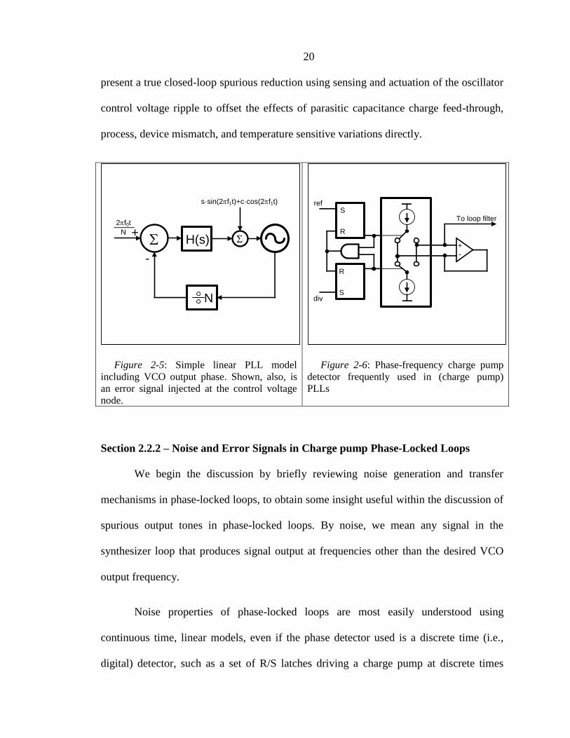
Figure 2-5: Simple linear PLL model including VCO output phase. Shown, also, is an
error signal injected at the control voltage node. .............................................................. 20
Figure 2-6: Phase-frequency charge pump detector frequently used in (charge pump)
PLLs .................................................................................................................................. 20
Figure 2-7: VCO control voltage waveform (red) and rectangular approximation ..... 33
Figure 2-8: Total power and fundamental power component in ................ 33
Figure 2-9: Charge pump schematic showing non-idealities that can affect the spurious
output performance of the PLL. ........................................................................................ 40
Figure 2-10: Control voltage (red) disturbances due to charge pump delay () and
current (I) mismatches as well as leakage. ..................................................................... 40
Figure 2-11: Distributing the charge pump output pulse of height A (top) to two pulses
of half height at twice the frequency ................................................................................. 45
Figure 2-12: Illustrating random charge distribution over two reference periods
resulting in four basis waveforms that are randomly switched between .......................... 45

xi
Figure 2-13: Conceptual illustration of the system-level closed-loop approach adopted.
........................................................................................................................................... 49
Figure 2-14: Block Diagram of the implemented system ........................................... 49
Figure 2-15: Detailed block diagram of the implemented PLL with all integrated
components ....................................................................................................................... 52
Figure 2-16: Static divide-by-two latch configuration (top), individual latch schematic
........................................................................................................................................... 53
Figure 2-17: Dynamic divider architecture and performance summary. ..................... 55
Figure 2-18: Simulated dynamic divider output phase noise. ...................................... 55
Figure 2-19: PFD block diagram; performance summary of PFD, CP and loop filter
blocks. ............................................................................................................................... 56
Figure 2-20: Simulated phase noise PFD (blue); contributions of PFD (green), loop
filter (red) to PLL noise, and sum total (black). ............................................................... 56
Figure 2-21: Charge pump schematic. ......................................................................... 58
Figure 2-22: Sampling detector block diagram, and input amplifier circuit detail. ..... 58
Figure 2-23: Simulated detector input stage gain and supply rejection. ...................... 60
Figure 2-24: Detected output for a 50MHz tone causing various modulation (incl.
produced fundamental spur) at 50MHz, 100MHz, 150MHz. ........................................... 60
Figure 2-25: Spur tone actuation circuit block diagram............................................... 61
Figure 2-26: Injected tone strength for first four harmonics. ....................................... 61
Figure 2-27: Analog trigger delay versus programming value .................................... 64
Figure 2-28: Chip micrograph of implemented PLL test-chip, including bond wires
and major circuit blocks. ................................................................................................... 64

xii
Figure 2-29: Signal power versus test-pulse injected timing ....................................... 66
Figure 2-30: Signal power versus test-pulse amplitude around an extremum. ............ 66
Figure 2-31: Simulated spurious tone reduction using four harmonics and eight
channels for ten different, random scenarios .................................................................... 67
Figure 2-32: Same for 16 harmonics and 32 pulses. .................................................... 67
Figure 2-33: Photograph of HEALICs PLL PCB, mounted on probe station. ............ 69
Figure 2-34: PLL test-setup overview.......................................................................... 69
Figure 2-35: PLL test-setup photograph. ..................................................................... 72
Figure 2-36: Reconstructed control voltage waveform before and after spurious tone
correction. ......................................................................................................................... 73
Figure 2-37: Output spectra at 10.4GHz before and after correction .......................... 73
Figure 2-38: Output spectra before and after correction at 12.0GHz .......................... 74
Figure 2-39: Output spectra before and after correction at 8.8GHz ............................ 74
Figure 2-40: Nominal and corrected fundamental spurious tone strength. .................. 75
Figure 3-1: Reproduced from [43], showing cutoff frequency in modern CMOS
devices versus gate length. ................................................................................................ 77
Figure 3-2: Reproduced from [43], showing technology node versus year of
production for Intel CMOS FETs. .................................................................................... 77
Figure 3-3: MOS varactor-based frequency up-conversion circuit (top) and model
(bottom)............................................................................................................................. 79
Figure 3-4: Capacitance versus voltage assumption made for circuit in Figure 3-3 .... 79
Figure 3-5: Simulated versus calculated conversion efficiency of an idealized MOS
varactor ............................................................................................................................. 81

xiii
Figure 3-6: Simulated conversion efficiencies of a MOS varactor from a 65nm design
kit ...................................................................................................................................... 81
Figure 3-7: UMC 65nm simulated and measured varactor resistance and capacitance
versus bias voltage, @20GHz. fc~280GHz. ...................................................................... 84
Figure 3-8: UMC 65nm simulated and measured varactor resistance and capacitance
versus bias voltage, @80GHz. fc~280GHz. ...................................................................... 84
Figure 3-9: Common source FET circuit (top) and model (bottom). ........................... 86
Figure 3-10: Output current non-linearity used for FET circuit of Figure 3-9. ........... 86
Figure 3-11: Harmonic components of output current ................................................. 86
Figure 3-12: Device voltage and current ...................................................................... 86
Figure 3-13: Simulated versus calculated fundamental power gain ............................ 92
Figure 3-14: Simulated versus calculated unity power gain cutoff frequency versus
duty cycle .......................................................................................................................... 92
Figure 3-15: Simulated first-to-second harmonic conversion efficiency versus
calculated .......................................................................................................................... 93
Figure 3-16: Simulated and calculated gain versus “a” ............................................... 93
Figure 3-17: Conversion loss (DC-to-second harmonic) for single oscillator (red) and
optimized oscillator-doubler combination (black), assuming no DC conduction in doubler
........................................................................................................................................... 98
Figure 3-18: Conversion loss (DC-to-second harmonic) for oscillator-doubler
combination at =0.6max (black) and =0.8max (red) versus doubler duty cycle. Lines
are values for simple oscillator. ........................................................................................ 98
Figure 4-1: Patch antenna layout................................................................................ 104

xiv
Figure 4-2: Simulated radiation efficiency and antenna gain .................................... 104
Figure 4-3: Simulated radiation efficiency ................................................................ 105
Figure 4-4: Antenna input impedance ........................................................................ 105
Figure 4-5: Quadrupler core design, lumped representation ...................................... 106
Figure 4-6: Layout simulation view of quadrupler core network .............................. 109
Figure 4-7: Basic amplifier stage schematic .............................................................. 111
Figure 4-8: Core amplification chain ......................................................................... 111
Figure 4-9: Simulated output power of core cell chain versus frequency ................. 112
Figure 4-10: System-level overview .......................................................................... 112
Figure 4-11: Simulated output frequency versus control voltage of center VCO...... 113
Figure 4-12: Simulated performance summary.......................................................... 113
Figure 4-13: IBM45nm die photograph ..................................................................... 114
Figure 4-14: Die photograph detail ............................................................................ 114
Figure 4-15: IBM PCB, mounted on stepper motor setup ......................................... 116
Figure 5-1: Antenna efficiency (radiation loss) shown for a dipole antenna of a lossless
Si substrate. ..................................................................................................................... 122
Figure 5-2: Antenna loss in dB for a dipole and a loop antenna on a semi-infinite,
lossy (10cm) Si substrate ............................................................................................. 122
Figure 5-3: Radiation loss of single dipole in UMC65nm process technology versus
substrate thickness .......................................................................................................... 124
Figure 5-4: Series addition of two frequency sources in series. ................................ 124
Figure 5-5: Top-level layout displaying the RF reference signal routing path .......... 131

xv
Figure 5-6: Doubler core cell set. The second harmonic signal current of each doubler
cell is routed from the common mode node through one of the two transformer primaries
to generate a voltage. The voltages are added in the output transformer secondary. ..... 132
Figure 5-7: IE3D view of output passive structures (input and output transformers).
Location of the doubler core and the fundamental signal input port(s) is also shown. .. 135
Figure 5-8: Schematics of buffer amplification stage. Feedback and input resistors are
used for stability. ............................................................................................................. 137
Figure 5-9: Top: output power versus core voltage. Bottom: output power versus
frequency......................................................................................................................... 137
Figure 5-10: Simulated conversion loss contours versus VSWR on Z0=300 Smith
Chart ................................................................................................................................ 138
Figure 5-11: Simulated output power contours versus VSWR on Z0=300 Smith
Chart ................................................................................................................................ 138
Figure 5-12: Core cell schematic including phase shifters and routing details.......... 140
Figure 5-13: Simulated output phase of single phase-shifter for different frequencies
versus control voltage. .................................................................................................... 142
Figure 5-14: Schematic of phase rotator. ................................................................... 142
Figure 5-15: Nominal supply voltages and currents .................................................. 144
Figure 5-16: Die photograph UMC65nm 250GHz 2 x 1 array chip .......................... 146
Figure 5-17: Die photograph UMC65nm 250GHz 2 x 4 array chip .......................... 146
Figure 5-18: 250GHz test-chip mounted in PLCC socket on test PCB. The PCB is
attached to a stepper motor to allow rotation around two axes shown (red arrows) ...... 147
Figure 5-19: Lens-based detection setup, shown here with calibration source.......... 147

xvi
Figure 5-20: Annotated DC biasing voltages on-chip example (set 3 out of 3 for the 2
x 1 test-chip) ................................................................................................................... 150
Figure 5-21: Thermal image of the 1x2 test-chip during steady-state biasing
conditions. The scale used with emissivity set to that of silicon corresponds red being
around 65oC. ................................................................................................................... 151
Figure 5-22: Close-up photo of 250GHz test-chip in PLCC socket on PCB. ............ 151
Figure 5-23: Measurement setup. Not shown is the Agilent E8257D signal generator
used to generate the LO signal, as well as the programming motherboard and the power
supplies. .......................................................................................................................... 152
Figure 5-24: 2x4 test-chip output power versus control voltage of phase rotator 28/32
......................................................................................................................................... 154
Figure 5-25: 2x4 test-chip output power versus control voltage of phase rotator 18/32
......................................................................................................................................... 154
Figure 5-26: Simulated gain (normalized) versus elevation angle for 1x2 test-chip
(rotation axis along dipoles)............................................................................................ 156
Figure 5-27: Measured gain (normalized) vs elevation angle for 1x2 test-chip. ....... 156
Figure 6-1: Multi-die stack packaging solution, offered by Amkor Technologies [76]
......................................................................................................................................... 163
Figure 6-2: Side and top view of dipole test structure. +/- indicate sides of a driving
terminal. .......................................................................................................................... 164
Figure 6-3: Optimal structure shape determination using software approach ........... 164
Figure 6-4: Radiation efficiency, optimal dipole in 250 micron Si lossless substrate at
height z (top of Si at z=250 micron) ............................................................................... 174

xvii
Figure 6-5: Antenna gain of 2D (blue) and 3D (red) dipole array as simulated (solid)
and predicted (broken). ................................................................................................... 174
Figure 6-6: Antenna gain resimulated for 3D case using sparser array. .................... 175
Figure 6-7: HFFS simulation setup for simulating 2D and 3D antenna arrays (3D
shown) ............................................................................................................................. 175
Figure 6-8: Bore-side array gain optimized for 2D, 3D cases ................................... 175
Figure 6-9: 45o elevation gain optimized for 2D, 3D cases ....................................... 175
Figure 6-10: 2D case 300GHz ................................................................................... 176
Figure 6-11: 3D case 300GHz ................................................................................... 176
Figure 6-12: 2D case 400GHz ................................................................................... 176
Figure 6-13: 3D case 400GHz ................................................................................... 176
Figure 6-14: 2D case 500GHz ................................................................................... 177
Figure 6-15: 3D case 500GHz ................................................................................... 177
Figure 6-16: Normalized antenna gain versus frequency for center driven reflectarray.
......................................................................................................................................... 177
Figure 6-17: Antenna gain versus frequency, active drive (impulse like) excitation. 177
Figure 6-18: Electronically tunable guidance through silicon ................................... 180
Figure 6-19: 2D guided radiation case. Top: maximum radiation, bottom: maximum
dielectric guidance .......................................................................................................... 180
Figure 6-20 : 3D guided radiation case. Top: maximum radiation, bottom: maximum
dielectric guidance .......................................................................................................... 182
Figure 6-21: Planar 2D arrangement for electronically tunable guidance through
silicon .............................................................................................................................. 182

xviii
Figure 6-22: Dielectric box, 2D control surface, entrapment mode. ......................... 184
Figure 6-23: Dielectric box, 2D control surface, radiation mode .............................. 184
Figure 6-24: Dielectric box with 3D control over radiation/entrapment. Here, the
radiation pattern for the entrapment mode is shown. ...................................................... 186
Figure 6-25: Dielectric box with 3D control over radiation/entrapment. Here, the
radiation pattern for the radiation mode is shown. ......................................................... 186
Figure 7-1: 1G phone, happy user (Dr. Martin Cooper). Taken from http://mm-
content-blah.blogspot.com/ ............................................................................................. 192
Figure 7-2: I-phone 3GS, considered state-of-the-art in 2010. Taken from:
http://www.apple.com/iphone/iphone-3gs/ ..................................................................... 192

1
Chapter 1 – Introduction
Section 1.1 – Wireless Systems
The last two decades have seen a prodigious increase in the spread and use of
electronic devices and gadgets in general, and wireless communication systems in
particular. In 1991, a cellular telephone was a bulky and expensive piece of equipment
that few could or wanted to afford. After all, it was difficult to imagine that anyone would
need to be available by phone around the clock. Twenty years later, children have cellular
phones, and it has become difficult to imagine what life was like when meeting a person
involved getting in contact well in advance of the planned meeting and agreeing on a
rather exact time and location. Similarly, driving to and around new locations involved
having to study paper maps rather than utilizing a GPS device. Similarly, other forms of
communication such as sending text messages, emailing, tweeting1 or signing in on
Facebook while being at a social gathering were all likely conceivable to a very small
group of people twenty years ago. Mobile devices such as the ubiquitous I-phone – which
among other gadgets has made the producer, Apple Inc., the largest company by market
capitalization in the U.S. – allow communicating, staying in contact, signing in or signing
off pretty much anywhere in the developed and the developing world.
This boom has only been possible with the continuous advances made in
semiconductor fabrication technology as well as digital and radio-frequency design
techniques and methodology. The advances in semiconductor processing are powered by
1 Tweeting=using “Twitter,” an online service that is used to broadcast to everyone what is on one’s
mind

2
an essentially insatiable demand for computing power and electronic storage capabilities,
as both allow ever increasing productivity, entertainment value, knowledge database
capacities and sheer endless possibilities to document and preserve one’s own life
memories in ever increasing detail and decreasing effort. Piggybacking on the advances
targeted at digital electronic systems are the analog and radio-frequency integrated circuit
designers that can use the increases in device speeds, integration densities and modeling
accuracy to develop ever faster, better and more powerful communication systems. In
parallel, the ever increasing availability of digital processing power allows the
deployment and use of ever more powerful CAD tools such as electromagnetic and
circuit simulation software that allow the modern analog design engineer to tackle and
simulate ever more complex problems and systems, since what was yesterday’s
supercomputer is today’s workstation and quite likely tomorrow’s handheld device.
This development brings its advantages as well as its disadvantages with it. As for
the advantages, we can expect tomorrow’s applications and wireless designs to operate at
higher frequencies, and using larger bandwidths, thus enabling entirely new applications
(some surely as of yet not conceived, as was the case twenty years ago with many of
today’s applications) in addition to greatly increasing the range of uses of current
applications. This ensures that analog designers will have many new problems to solve in
the years to come, as well as improving on known and proven designs. The disadvantage
of these developments is that they can tempt design engineers to use brute-force
approaches to old techniques that will only result in marginal improvements.

3
The above considerations motivate us to investigate new avenues, applications
and techniques for radio-frequency integrated circuit design to open some avenues and
start paving the way for these developments.
Section 1.2 – Frequency Synthesizers
In almost all communication systems and digital clock generation circuits,
reference signals at precise, controllable frequencies and of superior spectral purity are
required. Other applications require the generation of a clock-signal from an underlying
digital data stream. Over the years, the most common approach to generate these signals
for the above applications as well as many others has been to use phase-locked loops.
Because reference signals having the above characteristics are one of the few things
difficult if not impossible to come by in integrated circuits, a typical system requiring
such a signal will typically use an off-chip reference crystal that resonates at a known,
precise frequency. The characteristics of this reference crystal are then replicated for the
on-chip reference signals by phase-lock, such that the timing and accuracy of the on-chip
signal is determined by the off-chip crystal reference. A phase-locked loop is a natural
way to achieve this goal, and for this reason they are ubiquitous.
In the most common design, the comparison and actuation is done not in
continuous time but rather in discrete time since such a design approach is far more
amenable to a (mostly) digital implementation and control scheme. However, hand-in-
hand with smaller and faster devices due to the continuing advances in semiconductor
fabrication technology an ever increasing variability among the fabricated devices has
arrived because differences as small as a few atomic layers in a gate-oxide deposition

4
step will significantly change the device characteristics. The increase in variability
necessitates additional checks and/or additional control circuitry during the design to
ensure that this increased variability does not result in an increase in failure rates. For
phase-locked loops, the increased device variability can express itself increased parasitic
side-tones due to variations among nominally matched pairs of devices or gate-
capacitances. This increased variability has motivated DARPA to fund the HEALICs
program, a program designed to develop approaches to address problems arising from
this increase in variability and uncertainty. It also motivates us to investigate techniques
to mitigate the effect this increase in variability has on spurious side-tones in integrated
phase-locked loop synthesizers.
Section 1.3 – Sub-Millimeter Wave Systems
In addition to provide motivation to solving existing problems in existing
applications, we are furthermore motivated to investigate new approaches, techniques and
applications made possible by the advances in semiconductor fabrication technologies, as
well as advances in packaging technologies. An exciting area of current research in
integrated circuit design involves circuits and systems for millimeter wave applications.
Because at these frequencies (in the hundreds of gigahertz), no relatively inexpensive
solutions do yet exist, and providing such solutions could potentially open the way for
many new applications similar to the plethora of applications made possible only by
advances in integrated RF design previously. Besides new applications, traditional
applications such as wireless communication systems could be advanced significantly
such that applications as simple as connecting a high-definition television set to an
5
electronic media player – now accomplished via a cable – could potentially be
accomplished using a wireless radio with large bandwidth (as would be available in the
millimeter wave region). As far as new applications are concerned, many are currently
being investigated, such as millimeter wave imagers for security or diagnostic
applications.
This motivates us to investigate the challenges, limitations and opportunities of
CMOS integrated circuits for use in millimeter wave applications, as well as develop new
paradigms for designing systems at these frequencies, taking advantage of the fact that
the wavelength of electromagnetic signals at these frequencies is starting to again be
comparable to the physical dimensions of the circuits and systems designed to control
them.
Section 1.4 – Dissertation Organization
This dissertation is organized as follows: In chapter 2, mechanisms that cause
spurious tones, and known techniques to mitigate these tones in integrated phase-locked
loop synthesizers, are investigated. A novel technique is developed that utilizes a fully
closed-loop control approach, and demonstrated in simulation and experimentally.
In chapter 3, methods for generating millimeter wave signals using integrated
circuits based on CMOS technology are investigated and quantitatively described. Some
experimental results to corroborate simulation outputs with measurements are presented.
Theoretical calculations are corroborated using simulations, all with the goal of
developing tools and insight for the design of millimeter wave frequency integrated
CMOS circuits and systems.

6
In chapters 4 and 5, the design of two such systems is presented, applying the
insights gained in chapter 3. Challenges encountered and techniques used to address them
are described in the context of the design. Measurement results are presented to
corroborate the findings.
In chapter 6, three-dimensional integrated electromagnetic structures are
postulated and explored for applications in current and future integrated radio-frequency
systems. This proposition is motivated by challenges encountered during the design of
integrated circuit antennas, as well as motivated by potentially unexplored avenues of
integrated electronic design. These structures fit neatly into the recently proposed,
holistic design paradigm for millimeter wave silicon ICs [1].
The insights gained and the work accomplished will be summarized in chapter 7.
Possible avenues to develop the ideas presented further are presented and discussed.

7
Chapter 2 – Spurious Tone Detection and
Actuation in Integrated Frequency
Synthesizers
Section 2.1 – Introduction
Section 2.1.1 – History
The phenomenon of phase-synchronization or phase-locked systems is readily
observed in nature. Examples of phase-locked systems in the physical world include the
rotation of the moon around its own axis, which is phase-locked by the earth to its
rotation around it, such that only one side is visible from Earth. Another example is the
human sleep cycle, which is phase-locked to the length of the day with the free-running
cycle period slightly longer than 24 hours.
Man-made phase-locked loops (PLL) are negative feedback systems that lock the
phase of a reference signal to that of a local oscillator by comparisons of their respective
phases. The reference signal can either be at the same frequency as the local oscillator
signal or at any integer, rational or fractional (non-integer) multiple or fraction thereof.
The phase comparison can be made continuously or at discrete points in time, typically
upon zero crossings of the reference signal. The reference signal can be a periodic signal,
for example a crystal reference oscillator, or an aperiodic signal, for example a digital
data stream, from which the clock signal needs to be recovered.
8
The principle of phase-locked loops was first published in 1932 [2], while likely
conceived a year earlier. Publications of synchronization behavior of locked oscillators,
which is the principle behind the operation of a phase-locked loop, date back to 1923 [3].
Phase-locked loops started to be used widely for providing horizontal-sweep
synchronization for televisions [4] as well as for synchronizing the color subcarrier in
color-television systems [5]. In those days, the technique was referred to as an automatic
frequency- and phase-control system (AFC), using an acronym that describes the end
result (frequency- and phase-control) rather than the means of achieving it (phase-
locked), even though the technique is the same. With the reduction in cost of television
sets and the growing affluence of people first in the United States and then in the rest of
the Western World starting in the 1950s, television sets no longer were a luxury item that
only a few people could afford, but rather became a commodity item, and with that came
an increase in the study of the properties of the behavior of phase-locked loops [6]. On a
different front, frequency-modulated radio transmission became another application for
phase-locked loops, as phase-locked loops can be used to demodulate FM signals. FM
radio signal transmission was initially believed to not offer significant advantages
compared to amplitude-modulated (AM) transmission [7], until Armstrong [8] pointed
out that FM radio signals experience less noise interference compared to AM radio
signals. The spread of FM radio stations was further delayed by the Federal
Communications Commission decision to move the FM radio band from the 42MHz-
50MHz range to the 88MHz-108MHz currently in use, thus making older equipment and
stations obsolete. While earlier implementations of FM demodulators used tuned limiting
circuits that convert the frequency deviation to an amplitude such as the Foster-Seeley
9
Detector [9], [10], the usefulness of phase-locked loops for frequency demodulation was
certainly recognized and analyzed by the 1950s [6].
Section 2.1.2 – Uses of Phase-Locked Loops
Because of their versatility, phase-locked loops are used in a wide-range of
applications in wireline [11] and wireless communication systems [12] [13] in disk-drive
systems, instrumentation and high-speed digital circuits. In wireless communication
systems, phase-locked loops can be used to generate the local oscillator signal for both
the transmit chain and the receive chain, as well as radio-frequency (RF) signal
demodulators for frequency-modulated (FM) or phase-modulated (PM) signals [6].
Depending on the application, frequency references that are integer, rational or irrational
fractions of the local oscillator signal are used. In modern wireless communication
systems fractional-N synthesizers are most commonly used, as that allows the platform
design to use off-the-shelf crystal references at standard frequencies such as
3.579545MHz or 10.00MHz.
In now mostly older analog receiver systems, phase-locked loops can be used to
demodulate a frequency-modulated radio signal: when the local oscillator is locked to the
incoming radio signal, the phase-locked loop will produce a control voltage for the local
oscillator that tracks the instantaneous frequency of the radio signal [6].
In wireline communication systems, phase-locked loops in the form of clock
recovery circuits (CRC) can, as their name suggests, recover the clock signal from the
underlying data stream. For a random bit data stream, for which the underlying clock
frequency is specified to within a certain range, the clock can be recovered from the data
10
stream by comparing the phase of the local oscillator clock to the phase of a bit transition
whenever one occurs [14]. The phase detector in this case is implemented to keep track of
missing data transitions since the data bits will not transition on every clock cycle. The
same principle is used in disk-drive electronics to correctly time the data read by the
drive head as the platter speed varies.
Finally, phase-locked loops find applications in instrumentation equipment such
as signal spectrum analyzers to generate the various local oscillators to cover the input
signal frequency range desired, typically over many decades.
The usefulness of the phase-locked loop derives from a variety of its properties.
Historically, the reduction in cost of vacuum tubes and the introduction of the transistor
amplifier paved the way for the transition towards designing with a larger number of
simpler blocks compared to earlier designs, where each vacuum tube often served
multiple purposes for what engineers nowadays would design using separate, more
comprehensively designed individual system blocks. An automatic frequency and phase-
control system or phase-locked loop fits into this design paradigm, as the separate
functions such as loop filtering, phase detection and local oscillator signal generation are
separated in different functional blocks in the phase-locked loop. Besides this design
paradigm, phase-locked loops have characteristics that can be advantageously used in a
variety of applications.
One such advantage is the noise characteristics of phase-locked loops [15] [16],
which make them useful for a variety of purposes. Simply speaking, within the loop
bandwidth of the phase-locked loop, the noise of the local oscillator is determined by the

11
reference noise as the loop will control the local oscillator to track the reference. Outside
the loop bandwidth, no correction occurs and the noise is (mostly) the noise of the local
oscillators. Depending on which of the two has the better noise properties, different loop
bandwidths for the PLL are used, converting this property into an advantage. For radio
transmitter and receiver circuits, particularly for integrated ones, inexpensive quartz
crystal references provide excellent noise characteristics, and loops using wide
bandwidths are used to confer the noise properties of the crystal reference to the local
oscillator, reducing the overall jitter of the local oscillator accompanied and increasing
receiver sensitivity as well as lowering interference for transmitters. In clock and data
recovery circuits, the opposite is typically the case, where the incoming bit data stream
contains significant amount of timing jitter, caused by dispersion in the communication
channel in the case of wireline or clock distribution line channels or due to temporal
variations in the drive motor speeds in disk drives. Here, a phase-locked loop can be used
to reduce the jitter as the signal is retimed to a cleaner local oscillator signal, which is
locked at low bandwidth to the incoming data signal, to reject most of the high-frequency
jitter. Retiming can also be used to sharpen signal transition edges of incoming data
signals that have been corrupted during transmission, allowing the digital circuitry
following the receiver to operate at maximum speed as skew is reduced.

12
Figure 2-1: General phase-lock loop
Figure 2-2: Linear model for the general
phase-locked loop of Figure 2-1
Section 2.1.3 – Types and Operation of Phase-Locked Loops
A general block diagram of a phased locked-loop is shown in Figure 2-1.
Depending on how the individual blocks are implemented, different types of phase-
locked loops are generally distinguished. We briefly describe the operation of the phase-
locked loop using a simple linear negative feedback model (Figure 2-2) to describe a few
common implementation types of phase-locked loops. There exists a great deal of
background literature regarding the operation and analysis of phase-locked loops that we
will be referring to for further reading throughout.
A phase-locked loop most generally consists of a local, voltage-controlled
oscillator (VCO) and a mechanism actuating the control voltage based on comparing the
VCO phase to a phase reference. The oscillator produces a phase ramp that is the integral
of the input voltage times a gain constant (the oscillator gain , measured in Hz/V or
rad/V in the linearization). The output signal can optionally be divided or multiplied
fref PD
xLoopfilter
VCO
Divider
fVCO
Modulus
Generator
/N
H(s)S+
-
frefkv
s
fvco
fvco
N
k0

13
either by a rational or, in more modern implementations, fractional number, and the phase
of the divided/multiplied output is compared to a reference phase using a phase detector
(PD). In some implementations, the frequency as well as the phase are compared to each
other. The detector is then called a phase-frequency-detector. The output of the phase
detector is a voltage or a current that is typically filtered (or in the case of a current also
converted to a voltage) to produce the control voltage that controls the VCO, thus closing
the loop.
Depending on the implementation details, certain types of loops are distinguished.
For a simple analysis, we can linearize the operation of the loop and use well-known
methods for analysis of linear systems. This is appropriate [6] and sufficient for an initial
understanding of the operation. A linear, time-invariant (LTI) model of the loop is shown
in Figure 2-2. We can easily refer the output phase to the input phase (the reference
phase) with the closed-loop transfer function
( )
( )
(2-1)
A first classification distinguishes between two types of PLLs depending of the
form of ( ). So-called Type-1 (first-order) PLLs have a loop filter function that is just a
scalar (and thus contains no extra poles). The closed-loop transfer function then describes
a first-order system, and the resulting closed-loop transfer function is unconditionally
stable. Writing ( ) , we can write the transfer function as

14
(2-2)
The loop bandwidth is given by . The steady-state phase error for a
constant frequency input of the loop is given by Lee [17]
, thus, in order to minimize
the steady-state phase error, the bandwidth should be maximized. Thus, the advantage of
having an unconditionally stable loop response is offset by the steady-state phase error.
This error will result in an error signal constantly being injected, which is why first-order
PLLs are not frequently used, particularly when the PLL is using a charge pump-based
phase detector.
Figure 2-3: Root locus plot of a second-
order PLL with two poles and one zero in the
closed-loop transfer function, resulting from a
typical first-order loop filter implementation as
shown
Figure 2-4: Root locus plot with a second-
(third-) order loop filter. Broken lines indicate
locus when additional low-pass section is
included.
If the loop filter contains a single pole, the nomenclature speaks of a type-2 (or
second-order) PLL. In this case, the steady-state phase error is zero, at the expense of
x2
Im{s}
Re{s}x2
Im{s}
Re{s}x x

15
reduced stability, as the additional pole introduces another 90o phase-shift. The loop then
has two poles on the imaginary axis, and needs to be stabilized using an additional zero.
A typical (analog) loop filter having a DC pole and a (non-DC) zero consists of a series
resistor and capacitor. The loop will always be stable, as the poles for any positive loop
gain will lie in the left-hand side of the s-plane (see Figure 2-3). Typically, the large
voltage produced over the zero-setting resistor is undesirable, as it affects the headroom
of the phase detector during acquisition (and, hence, limits its dynamic range), and can
also be a source of significant noise. Therefore, an additional pole can be introduced by
adding a parallel capacitor. Oftentimes, an additional low-pass section with a high-cutoff
frequency is added as well. The cutoff frequency is chosen such that the additional phase
delay is minimal within the loop bandwidth. The resulting second- or third-order loop
filter results in an overall third- or fourth-order loop response. The root-locus of a PLL
using such loop filters is shown in Figure 2-4, with the broken lines in the locus showing
the impact of the additional low-pass section. As can be gathered from the locus, for the
second-order loop filter, the loop is stable, but with poor phase margin at both low and
high loop gains. For the third-order loop filter, the loop filter becomes unstable for very
high loop gain. In synthesizers that operate over a range of output frequencies, the loop
gain can vary considerably over the range of operation frequencies (due to different VCO
gains mostly, but also oftentimes due to different division ratios). As a result, the
transient response often exhibits regions of good damping as well as regions where some
ringing can be observed, typically at both edges of the operating region.
Having discussed the different types of PLLs based on the transfer function, we
make an additional distinction based on the type of phase detector used. Historically,
16
mixers were used as phase detectors, as they were easily implemented in all analog
implementations. When the inputs are at the same frequency, the mixer will produce a
DC output that is a function of the phase difference of the two input signals, such that
( ) (2-3)
Thus, in steady-state the (divided) VCO output phase is locked to the reference
phase in quadrature. Several issues arise with the use of a mixer as a phase detector. First,
when and are more than 90o out of phase, the transfer function has a negative
slope, turning the phase-locked loop into a positive feedback system. Secondly, a mixer is
a phase-only detector, and its overall DC output is zero should the frequencies vary. For
small variations in VCO and reference frequency, and assuming the loop starts in a
locked state, the phase difference grows slowly, such that the loop will reacquire lock
before the difference grows larger than 90o. Thirdly, the gain of the phase detector is non-
linear, growing smaller as the phase difference grows, and – as we just saw for higher-
order loops – reducing or even eliminating stability for phase differences even less than
90o. For these three reasons, the large-signal response of the phase-locked loop is non-
linear, and signal acquisition can be tricky if the initial phase- and/or frequency-
difference is large (or if the loop is making a large step). Analyses of the non-linear
acquisition behavior has been studied here [18] for simple type-I and type-II PLLs.
Distortion effects due to non-linearities in higher-order PLLs are studied here [19].
Because a phase- and frequency-detector provides the phase-locked loop with a
larger acquisition range, and because of the digital nature that is more amenable to
modern integrated process technologies, charge-pump-based phase-locked loops

17
incorporating sequential logic phase-frequency detectors have become a popular
alternative since at least the early seventies [20]. In a charge pump-based PLL, the phase-
frequency detector detects the phase-difference between the (divided) VCO signal and
the reference input at discrete time points (typically at the zero crossings of the two
signals) and produces a non-zero output current in the time-window between the two
crossing, such that the total charge pumped into the loop filter is proportional to the phase
difference. A charge pump-based PFD has positive DC gain for any phase-difference as
well as frequency-difference, and is therefore capable of detecting frequency, hence the
larger acquisition range. Because the comparison is made at discrete time instances, the
simple linear model above is improved upon by replacing it with a discrete time system
model [20] [21]. In order to more accurately model the transient response of a charge
pump phase-locked loop, the transfer characteristic of the detector is linearized to take
into the account the frequency shift that the VCO experiences while the pump is active.
Because the actuation is accomplished at discrete time instances rather than continuously,
the VCO control voltage is perturbed periodically even in lock due to non-idealities such
as charge kick-back, modulating the VCO output to produce discrete spurious side-tones.
Reducing this spurious output to a minimum is a goal of phase-locked loop designers and
a novel technique the topic of this chapter.
By analyzing the true discrete time nature of the loop, loop stability calculations
reveal lower phase margins than what is expected from a linear, continuous time model.
This is expected as the discrete time nature introduces an additional delay in the loop, for
when the charge pump is inactive, any phase-difference is not immediately actuated,
hence the delay. Not surprisingly, the difference in calculated phase margin becomes
18
larger as the loop bandwidth increases as the delay between roughly each reference clock
cycle corresponds to a larger phase around the loop bandwidth.
In closing this section, we note that the generation of a divided VCO zero-
crossing can be accomplished in a variety of ways. Most often, a digital counter –
possibly programmable – is used to produce an edge every edges of the VCO signal
(thus dividing the phase by ). To obtain fractional counts, the value of is frequently
changed between several integer values such that the average count is a fractional value.
The method of changing is a typically a quasi-random dithering methods optimized to
push the resulting dithering noise away from low frequency (where it would appear at the
VCO output) to high frequencies [22]. An interesting alternative approach is to simply
use a windowed version of the VCO signal such that only every th edge is visible to the
phase-frequency detector [23].
Section 2.1.4 – Overview of Implemented PLLs
As part of the thesis work, three PLLs systems were implemented. The first set of
PLLs (low-band and high-band) were part of the AMRFC program funded by ONR
implemented in a 130nm CMOS by IBM. The PLLs operate from 5-7GHz and from 9-
12GHz to produce LO signals for two receiver chains covering frequencies from 6-
18GHz [24]. The PLL circuit implements some experimental circuitry to affect the dead-
zone of the phase-frequency detector [25]. The implemented receiver and synthesizers
served as a reference design for a second set of PLLs funded by DARPA as part of the
HEALICs program (“self-healing” ICs) [26], which are the main topic of this chapter.
The PLLs for the HEALICs program were implemented using IBM’s 65nm low-leakage
19
CMOS process. A third test-chip PLL was implemented in UMC’s 65nm CMOS process
to test some of the ideas for the HEALICs PLL.
Section 2.2 – Background – Noise and Spurious Output Tones
Section 2.2.1 – General Considerations
Spurious tones in phase-locked loop (PLL) synthesizers are undesirable for many
reasons: in radio transmitters, spurs are transmitted alongside the RF carrier, interfering
with users in adjacent channels. In radio receivers, spurs down-convert signals in adjacent
radio channels to base-band, causing interference and degrading sensitivity. In clock-and
data recovery circuits that use PLLs (e.g., [27]), spurs can cause increased bit-error rates
in the recovered data due to edge-transition timing inaccuracies in the recovered clock. In
fractional-N synthesizers, reference spurs in the oscillator output are dithered alongside
the main tone, resulting in increased synthesizer noise.
Side-tone spurs in synthesizers are typically introduced through frequency-
modulation (FM) of the carrier signal, and are more problematic than amplitude-
modulated (AM) tones as gain limiting operations attenuate AM spurs. In PLLs, the
voltage-controlled oscillator (VCO) is typically FM modulated by periodic disturbances
of the control voltage due to the loop action. In practice, many techniques are employed
to reduce the disturbance: use of sample-and-hold loop filter [28], feedback-based
methods to reduce charge pump mismatch [29], methods reducing the VCO gain upon
lock [30], and methods to adjust the timing of control voltage actuation with subsampling
phase detectors [31]. All of the above methods attempt to either minimize the control
voltage ripple in an open-loop fashion or the resulting FM modulation. In this paper, we
20
present a true closed-loop spurious reduction using sensing and actuation of the oscillator
control voltage ripple to offset the effects of parasitic capacitance charge feed-through,
process, device mismatch, and temperature sensitive variations directly.
Figure 2-5: Simple linear PLL model
including VCO output phase. Shown, also, is
an error signal injected at the control voltage
node.
Figure 2-6: Phase-frequency charge pump
detector frequently used in (charge pump)
PLLs
Section 2.2.2 – Noise and Error Signals in Charge pump Phase-Locked Loops
We begin the discussion by briefly reviewing noise generation and transfer
mechanisms in phase-locked loops, to obtain some insight useful within the discussion of
spurious output tones in phase-locked loops. By noise, we mean any signal in the
synthesizer loop that produces signal output at frequencies other than the desired VCO
output frequency.
Noise properties of phase-locked loops are most easily understood using
continuous time, linear models, even if the phase detector used is a discrete time (i.e.,
digital) detector, such as a set of R/S latches driving a charge pump at discrete times
N
H(s)S+
-
s·sin(2pf1t)+c·cos(2pf1t)
2pf0t
NS
+
-
div
STo loop filter
R
S
R
ref

21
(compare Figure 2-6). Good analyses using such an approach can be found here [32] and
here [15]. We will briefly summarize the findings here.
The phase-locked loop is a feedback system, and its output noise is determined by
the contribution of the individual blocks within the PLL (the most important ones being
the VCO, the divider and the loop filter) as well as the noise contributed by the reference.
Each of these contributions is shaped by the closed-loop transfer function of the loop.
A linear analysis ignores that a phase-locked loop typically uses a sampling
phase-frequency detector, so phase comparisons are made at discrete points in time,
typically coinciding with rising-edge zero crossings of the divided VCO output and the
reference signal. Figure 2-5 shows a simplified model. We would like to analyze the
effect of a single tone in the output phase of the VCO, so the divide-by-N output phase is
given by
( ( ) ( )) (2-4)
The phase-frequency detector and the charge pump are lumped into the summing
device. Let be the charge pump current. We make the simplifying assumptions that
the input reference phase is noiseless and that the phase comparison is done
instantaneously whenever the reference phase is a multiple of . The noise of the
reference can be approximated by adding it to the output of the divider.2 The output of
the phase-frequency detector/charge pump blocks is then given by
2 In a fully linear model, those two noise contributions are indistinguishable.

22
∑ (
) (
[ ( ) ( )]
)
(2-5)
with the further assumption that is given by the sine and cosine terms, i.e.,
that s and c are sufficiently small. H denotes the Heaviside function:
( ) {
(2-6)
Equation (2-5) is a transcendental equation without a general solution that takes
into account the feedback. Furthermore, we have ignored any DC components for now,
which, in the closed-loop system will be zero. However, whenever and are related
by a rational multiple, the infinite sum can be split up into multiple infinite sums of the
form
∑ ∑ ( ( )
) (
( )
)
(2-7)
where is the least common multiple of
, and are constants that
can be determined numerically. Since the phase-locked loop is a frequency modulator,
the question arises whether it is self-demodulating, that is, if the spurious output at the
VCO is demodulated onto the control voltage so that the loop is its own detector so to
speak (the answer is, unfortunately, no, as will be explained shortly). Secondly, we would
like to illustrate noise folding that takes place in the loop.
We first investigate how spurious output tones present at the VCO output are
demodulated. All spurious outputs are at integer multiples of the reference frequency,
hence . (2-7) simplifies for all , however, to
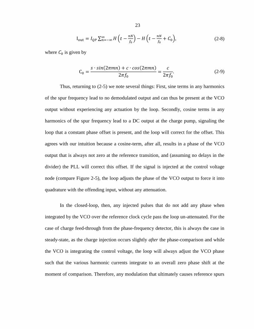
23
∑ (
) (
)
, (2-8)
where is given by
( ) ( )
(2-9)
Thus, returning to (2-5) we note several things: First, sine terms in any harmonics
of the spur frequency lead to no demodulated output and can thus be present at the VCO
output without experiencing any actuation by the loop. Secondly, cosine terms in any
harmonics of the spur frequency lead to a DC output at the charge pump, signaling the
loop that a constant phase offset is present, and the loop will correct for the offset. This
agrees with our intuition because a cosine-term, after all, results in a phase of the VCO
output that is always not zero at the reference transition, and (assuming no delays in the
divider) the PLL will correct this offset. If the signal is injected at the control voltage
node (compare Figure 2-5), the loop adjusts the phase of the VCO output to force it into
quadrature with the offending input, without any attenuation.
In the closed-loop, then, any injected pulses that do not add any phase when
integrated by the VCO over the reference clock cycle pass the loop un-attenuated. For the
case of charge feed-through from the phase-frequency detector, this is always the case in
steady-state, as the charge injection occurs slightly after the phase-comparison and while
the VCO is integrating the control voltage, the loop will always adjust the VCO phase
such that the various harmonic currents integrate to an overall zero phase shift at the
moment of comparison. Therefore, any modulation that ultimately causes reference spurs

24
will not be corrected by the phase-locked loop or detectable if its origin is not modulation
of the VCO control voltage itself.
The phase-locked loop reacts similarly to spurious tones generated outside the
feedback loop, most notably due to supply and substrate signals modulating the VCO
output through AM-to-PM conversion. Thus, the phase-locked loop will not act as a
spurious tone detector by itself. Furthermore, the divided VCO edge will always be
aligned with the reference edge, and it will contain no further information useful to any
secondary demodulating loop other than its DC value (as a proxy of duty cycle), which is
indicative of the strength of the remaining sine-term at the reference fundamental or
properly aliased terms at the reference fundamental and the harmonics.
For cases where the error signal is at a frequency other than the reference
frequency or any of its harmonic, we treat the case of a rational fraction. Again,
substituting
(2-10)
we obtain
( ) (
) ( ) (
) (2-11)
We can separate the sum in (2-5) into the double sum of (2-7) with given by
the least common multiple of and after all common factors have been cancelled.
Several separate cases are perhaps of interest, the first where the noise contributor is well
within the loop bandwidth, the second where the contributor is close to the reference
frequency or its harmonics and the third where the contributor and any of its mixing

25
products are outside the loop bandwidth. This third case yields a good example. Let be
an odd natural number and . Then (2-7) can be simplified to
∑ ∑ ( ( )
) (
( )
)
(2-12)
with
( ( )) ( ( ))
(2-13)
so that
∑ (
) (
( )
)
(2-14)
Sine terms do not appear as the introduced phase-shift at each comparison point is
precisely zero. We note that the function is periodic with period
, and we can determine
the spectral content by determining the Fourier series of
{
(2-15)
which has the following Fourier coefficients:
[ (
) (
) (
)] (2-16)
As we can see, the PFD mixes an input signal at half the reference frequency with
the reference frequency, to produce output at half the reference frequency as well as its
26
harmonics. Thus, noise originating at half the reference frequency will be redistributed.
Noise analyses, such as references [16], ignore this frequency translation.
By the same token, noise that is originally located at low frequencies (where it
would have been attenuated by the loop) will be partially up-converted to outside the loop
bandwidth (close to the reference frequency).
Section 2.2.3 – Spurious Output due to Oscillator Control Voltage Modulation
In this section we shall derive some useful relationships between periodic
transient disturbances of the oscillator control voltage and the resulting spurious output.
Because the control voltage oscillator acts as a phase-integrator, transients on the control
voltage introduce frequency modulation at the VCO output. Because the disturbances
discussed are periodic in nature, the resulting modulation of the VCO output is also
periodic with the same periodicity.
Introductory texts [3] typically treat the case of single-tone sinusoidal
disturbances and derive the resulting output spectrum with the additional assumption of
high oscillator frequency (so to neglect aliasing). We will be using the assumption of a
large oscillation frequency compared to the disturbance as well.
For the purpose of the discussion in this section, we assume a linear relationship
between oscillator frequency and control voltage. Furthermore, we set the nominal
control voltage to zero volts, at which the oscillator operates at a frequency . The
oscillator is assumed to have a gain (measured in Hz/V) such that the instantaneous
27
oscillation frequency is ( ) when the instantaneous control voltage is . The
oscillator output voltage is then given by
( ) [ (∫ ( )
)] (2-17)
where we have assumed an output voltage of one.
Because the disturbance ( ) is periodic, we expand ( ) in a Fourier series. Let
denote the division ratio in the phase-locked loop such that the period of ( ) is
; we
can then write:
( ) ∑ [ (
) (
)]
(2-18)
such that (2-17) can be written as
( ) [
(∑
[ (
) ( (
) )]
)] (2-19)
From equation (2-19) we can derive several useful insights. We first calculate the
spurious tone output power generated by a single tone. This leads to the well-known
result that the strength of the th harmonic side-tone is the value of the Bessel function of
first kind at the modulation index. Let . ( ) can
then be written as

28
( ) [ (
)
] (2-20)
We further assume3 than N>>1, such that a base-band representation can be used
with the base-band signal being
( ) [
(
)] [
(
)] (2-21)
From equation (2-21) we can derive the spurious output harmonic components.
To do this, we calculate the th Fourier component at baseband. We note that ( ( ))
has a period of , whereas ( ( )) has a period of . Since, furthermore,
( ( )) is anti-symmetric around , whereas ( ( )) is symmetric, only one
contribution in each integration, and we obtain
{
∫ (
) [ (
)
]
∫ (
) [ (
)
]
(2-22)
In both cases, , the Fourier coefficient of the th sideband, evaluates to
(
) (2-23)
where is the Bessel Function of the first kind and th order.
3 This assumption – which seems to always be made – is a form of the Riemann-Lebesgue lemma,
which states that ∫ ( )
as , provided that ∫ ( )
exist. See [80].

29
Using , the same result is obtained, except
that both sine and cosine terms in (2-21) contribute power. For all cases with exactly one
coefficient or non-zero, we obtain (
).
Thus, the amplitude and the carrier at
for single-tone
frequency modulation are given by
(
) except for m=0 where
(
). The term in parentheses is the modulation index. Because
∑
( ) , we deduce that power is conserved and that the power not present in
the carrier is spread to the sidebands.
From the above discussion, it is clear that when comparing the spurious output of
two phase-locked loops, a figure-of-merit needs to take into account the PLL division
ratio as well as the ratio of VCO gain to operation frequency. Furthermore, we note that
higher harmonics of the signal perturbing the control voltage cause lower spurious output
power due to their lower modulation index.
This motivates us to develop a formula for total sideband power as a function of
the harmonic power in the modulating signal. We will find an approximate solution based
on the assumption that the overall perturbation is small.
Without loss of generality, we rewrite (2-19) with modulation components in
quadrature, which corresponds to the case where the sine and cosine components in (2-
19) start with the same phase a quarter cycle apart. Then,

30
( ) [
(∑
[ (
) (
)]
)] (2-24)
and, using complex notation and assuming N>>1, the base-band signal can be written as
( ) [
∑
[ (
) (
)]
] (2-25)
where we have introduced a perturbation parameter with the idea of letting in
order to analyze the perturbation the harmonic components have on each other. The
Fourier component of the mth
component is
∫ (
)∏ [
[ (
) (
)]]
(2-26)
Using a series expansion for the term under the integral in powers of , it reads
(
)( ∑
[ (
) (
)]
) ( ) (2-27)
The only first-order terms to evaluate to a non-zero term after integration occur
for n=m, hence, for small modulation indexes, we can approximate the mth
Fourier
component in the series using (2-22) and approximate the total spurious power as
∑ (
)
(
)
(2-28)
Thus, for small valued modulation indices at all harmonics in the control voltage
perturbation waveform ( ), we reduce the total spurious power most effectively by
weighing the harmonic components in ( ) according to the inverse squared of their
harmonic number. In other words, a component at twice the offset frequency from the
31
carrier should be weighed with a weight of 1/4th
compared to the fundamental if the goal
is overall spurious power reduction. This observation agrees with our intuition that the
integrating nature of the oscillator attenuates perturbations.
At large values for the modulation indexes – when the assumptions above are no
longer valid – the total spurious power is a non-linear function of the modulation indices.
This means that increasing the modulation index can actually lead to a decrease in the
total spurious power. This is even predicted by the single-tone case, as ( ) has a zero-
crossing for finite . More formally, we note that the fundamental power is given by
∫ ( ) ( )
(2-29)
where V( ) can be written as
( ) [
(∑
[ (
) (
)]
)] (2-30)
Taking the derivative w.r.t. any or , e.g., , we note that the derivative itself
is a function of all the other coefficients, and it can be greater than zero, such that the
fundamental power increases with increasing modulation coefficients. Thus, linearity of
signal-to-output power should only be assumed for small modulation coefficients.
With this background, we will now investigate practical approaches for reducing
the spurious power in phase-locked loops.

32
Section 2.3 – Problem Approaches
Section 2.3.1 – Actuation of Spurious Tones – General Considerations
In the sections to follow, we will assume that all spurious synthesizer output is
caused by perturbations on the control voltage waveform and that we are sensing the
spurious output of the synthesizer by measuring this perturbation. This assumption is not
necessary, and the techniques discussed work similarly well if the output spurious content
is measured differently, for example, through FM demodulation of the oscillator output.
In particular, the control voltage waveform harmonic content should be weighed to
reflect the fact that the same signal strength at a higher harmonic results in a lower
modulation index and, hence, a lower output spur.
As previously mentioned, the approach ultimately used allows for determination
of the spurious content at each offset frequency, and can therefore be pre-weighted in a
variety of ways. For example, as mentioned above, components at higher harmonics
modulate the VCO output with a lower modulation index (producing less spurious
power), and should thus be weighed accordingly. Finally, oftentimes the largest output
spur is of importance, thus a weighing function could consist of the maximum spurious
component power only. In our approach, we ultimately weighed the components
according to the total produced spur power.

33
Section 2.3.2 – Actuation of Spurious Tones by Injecting Rectangular Pulses
Figure 2-7: VCO control voltage waveform
(red) and rectangular approximation
Figure 2-8: Total power and fundamental
power component in ( ) ( )
In this section, we consider the effect of adding rectangular pulses to the control
voltage waveform in order to minimize the spurious tone content of the voltage
controlled oscillator. While it is difficult to generate truly rectangular pulses in practice,
this discussion will illustrate some important aspects of attenuating output spurious tones.
Figure 2-7 shows a depiction of one period of a control voltage waveform ( ) as
illustration. Since we are only interested in the time-varying component, the DC value is
subtracted, such that the waveform has zero average value. The waveform is periodic
with period with one period shown. The period is divided into equally
sized parts of duration . For the example in Figure 2-7, is eight. Shown also is
an approximation of the waveform using rectangular pulses. For reasons that will
become clear shortly, the height of each rectangular pulse is chosen to be the average
value of the waveform in the mth
time-window (m=1, 2, ), such that
Time t [A.U.]
Vo
ltag
e [A
.U.]
Tref
Control Voltage Vc(t)
Approximation Vr(t)
-70
-60
-50
-40
-30
-20
-10
0
1 10 100
Po
we
r R
ed
uct
ion
[d
B]
Number of PWL Sections
Waveform Power after PWL Subtraction
Total Power
Fundamental

34
( ) ∑ ∑ ( )
(2-31)
where ( ) is given by
( )
{
∫ ( )
( )
( )
(2-32)
Because the waveform is periodic, we perform all calculations over a single
reference period. The (average) power of ( ) is given by
∫ ( ( ))
∑ ∫ ( ( ))
( )
(2-33)
where a constant of proportionality has been set to one. We would like to approximate
( ) by a piecewise constant function ( ) such as to minimize the power of the
difference between ( ) and the piecewise constant function, that is, we find the for
each m with
( ) {
( )
( )=
( )
(2-34)
such that the power in the difference function ( ) ( ) is minimized in each section.
Thus,
35
∫ ( ( ) )
( )
∫ ( )
( )
(2-35)
where we have used Leibniz’s Integral Rule, i.e., assuming that ( ) is
continuous and differentiable. Hence, we recover Eq. 2-32 and find that ( ) ( ),
motivating our choice for approximating ( ) section by the average values over the
piecewise regions.
As the number N of sections is increased, the approximation to the function ( )
improves, where the metric of improvement is the difference in power. We can gain
quantitative insight into the improvement by assuming ( ) is a sinusoid with periodicity
for the moment. Without loss of generality, we set to one, and by integrating
( ( ) ( )) over one reference period, it can be shown that the total power in the
difference between the true waveform ( ) and the piecewise-linear approximation ( )
is given by
( )
[ (
) ]
(
) (2-36)
where denotes the number of linear sections in the piecewise-linear approximation.
The total power in the difference signal drops of with the square of the number of
sections used. Incidentally, the fundamental component in the difference ( ) ( ) is
given by
( )
[ (
) ]
(
) (2-37)

36
hence the power in the fundamental component drops with the fourth power of the
number of sections used. These relationships are plotted in Figure 2-8 for approximations
with up to 64 sections. The values for two and four sections are identical because the
approximation is identical due to the symmetry in the sine wave shape. The remainder of
the power is shifted to higher harmonics, with the lowest harmonic containing power
being one number below the number of sections used. Hence, the remainder of the power
is shifted to increasingly higher harmonics as more sections are used. However, at least
two sections need to be used to provide any reduction by Nyquist’s Theorem. In general,
we therefore need to use pulses to actuate the first harmonics.
Section 2.3.3 – Actuation of Spurious Tones by Injecting Arbitrary Waveforms
In this section, we are going to discuss an approach that is more amenable to
practical implementation as well as more effective for a given resource overhead used to
mitigate spurious output.
From the discussion of Section 2.3.2 – Actuation of Spurious Tones by Injecting
Rectangular Pulses, we note that if reduction in the output spurious power is our goal, we
achieve a higher return for our efforts at lower harmonics. However, dividing the
reference clock cycle into equal time slots puts more emphasis onto the lower harmonics
than required, since – as we noted in the previous section – the harmonic reduction drops
off as the fourth power with the number of slots used, that is for a given number, we
expect the fundamental to be attenuated by 12dB more than the second harmonic. From
our discussion in Section 2.3.1 – Actuation of Spurious Tones – General Considerations,
however, we would like to more evenly reduce the harmonics (with the difference in

37
power between the harmonics being 6dB per octave). In practice, the situation is not quite
as dire, as the synthesizer loop filter adds additional reduction to higher harmonics, as it
is much easier to filter out high harmonics of the reference clock from the control voltage
than lower harmonics. In particular, strong attenuation of the fundamental by the loop
filter will typically introduce noticeable phase shift within the loop bandwidth, leading to
degradation of loop stability as well as noise performance due to jitter peaking.
In some sense, therefore, we are mostly interested in eliminating the Fourier
components of the first few harmonics in the control voltage waveform and using a loop
filter that has steep attenuation at frequencies that are large compared to the reference
frequency. In a limiting sense, we are interested in eliminating the first few harmonic of
the reference spurs, knowing that the remaining components are going to be negligible
and/or easily removed using a high-order loop filter with a high cutoff frequency
compared to the reference frequency.
Assuming we are interested in eliminating harmonic components of the reference
frequency from the control voltage waveform, we again use rectangular pulses as a
starting point. If all we are interested in is eliminating the fundamental component, we
immediately realize that we only need to inject one pulse, as long as we have absolute
control over the timing and the amplitude. This is because the Fourier series for the pulse
contains a fundamental component, and as long as the amplitude is the same as the
fundamental component present in the perturbing waveform and the phases are opposite,
the sum of the two waveforms contains no fundamental component. The price we pay is,
of course, potentially larger power at higher harmonics. In some sense, this has been the

38
approach all along, since injecting N rectangular pulses reducing the overall harmonic
power we may have increased the power at high harmonics than the original waveform
contained as a price paid to reduce the overall power. If instead of weighing the power
evenly at all harmonics, we apply a weighting function that assigns zero weight to the
power at harmonics above a cutoff, we would be using the same approach. So, if we
could use one rectangular pulse only, but we only wanted to eliminate the fundamental
component, we would simply assign a weight of one to the fundamental component and
zero to all other components. Then, to the sense circuitry used, both the injected pulse as
well as the measured perturbation of the control voltage would appear as pure sine waves,
and a power reduction feedback algorithm would be able to eliminate all (measured and
weighted) power using just one pulse.
The situation gets more complicated when the control voltage as well as the
injected waveform contains multiple harmonics, and the goal is to eliminate the first N
harmonics. We start considering the case where both the control voltage perturbation
waveform as well as the injected pulse waveform contain two harmonics. We use real
notation with phase and amplitude. We can write
( ) ( ) ( )
( ) ( ) ( ) (2-38)
where we only express the phase difference between the fundamental and the second
harmonic as a parameter. We assume that two pulses ( ) are injected at precisely
controllable times in the reference clock cycle. Expressing the times as phases of the
fundamental, we write

39
( ) ( ) ( ) (2-39)
and solve using harmonic balance. Hence,
( ) ( )
( ) ( )
( ) ( ) ( )
( ) ( ) ( )
(2-40)
There are four equations and four unknowns, namely . However, this
system is underspecified. Namely, from the second equation we deduce
( )
( )
(2-41)
and from the first
( )
( )
( )
( ) (2-42)
If we now assume that and , the third equation reduces to:
( ) ( ) ( ) ( ) (2-43)
which only allows as a solution and hence . We need to pick
whenever This reduces the first and the fourth equation to
( ) ( ) ( )
(2-44)

40
Hence, the system is underspecified, as no solution exists in the case chosen if
Only in special cases are two pulse injections sufficient to completely eliminate
the first two harmonics.
In order to eliminate the first N harmonics given an arbitrary injection pulse
waveform that can be time-shifted, 2N such injection pulses need to be given (assuming
that the pulse contains components at all harmonics).
Figure 2-9: Charge pump schematic
showing non-idealities that can affect the
spurious output performance of the PLL.
Figure 2-10: Control voltage (red)
disturbances due to charge pump delay ()
and current (I) mismatches as well as leakage.
Section 2.3.4 – Prior Approaches for Spurious Tone Minimization and Cancellation
In this section we will discuss approaches and strategies taken previously to
minimize spurious tone output, present our approach, which – to the best of our
knowledge – is the first fully closed-loop system-level approach, and compare our
approach to other approaches found in the literature.
+
-
down
To loop filterup
+
I0
I0+I
Ileak
Tref
Co
ntr
ol V
olt
age
[V]
Time
I
Leakage
41
We begin our discussion by noting charge pump matching issues. The charge
pump circuit typically consists of a pair of current sources, one sourcing current into the
loop filter and one sinking current into it. Each of these currents is controlled separately
by the PFD up and down outputs, respectively. This is shown in Figure 2-6, which is
repeated here as Figure 2-9 with three types of common additional non-idealities shown
that can affect the spurious tone production: (1) Delay mismatches in the propagation of
the PFD “up” and “down” signals to the current source switches, (2) mismatches in the
“up” and “down” currents produced by the charge pump, and (3) leakage current at the
charge pump output.
Propagation delays from the outputs of the PFD are inevitable, as finite switching
times imply delays. A related phenomenon is that of a PFD dead-zone, which occurs
when the delay becomes larger than the time required for PFD reset. In this case, the
charge pump PFD produces no output for small phase offsets between the reference
signal and the VCO signal. We will return to this phenomenon a few times. First,
however, a difference in the delay produces a non-zero output waveform in steady-
state as the loop will need to introduce a small phase offset between the reference phase
and the VCO phase to compensate for this delay difference. The resulting steady-state
charge pump output current waveform is shown in Figure 2-10. Great care in the design
of the charge pump circuit is typically taken to ensure minimal delay differences. In
integrated charge pump design, the fact that the “up” and “down” switches typically
require differently doped devices (i.e., NFETs and PFETs in CMOS) makes this problem
more challenging, and various strategies involving dummy devices can be employed.

42
The second issue that can produce a much larger reference spurious tone is a
mismatch between the “up” and “down” currents. A DC mismatch typically occurs due to
non-ideal current mirrors as well as finite output resistance of the current sources that
introduce small variations in the output currents depending on the control voltage value.
Furthermore, finite switching transients shape the output current waveform transients
such that transient differences between the “up” and “down” current may exist, again a
problem that is made more difficult by the requirement for using different device types
(with different transient behavior) for the up and down currents. The PLL, again, will
compensate by introducing a small phase offset such that net deposited charge onto the
loop filter is zero in steady-state, which can result in non-zero transient currents. Figure
2-10 also shows the charge pump output waveforms due to DC current offsets as well as
transient differences. DC current offsets are typically addressed using servo loops that
within the charge pump control any offsets to an absolute minimum.
Finally, any DC leakage current present in the charge pump or loop filter requires
an offsetting net DC current to be provided by the PLL. This DC current, however, will
also introduce AC currents that produce an AC perturbation on the control voltage line
and with it output spurious tones. Again, compare Figure 2-10.
All of the above issues share in common that the PLL will introduce phase offsets
such that the net charge deposited onto the loop filter is zero (excluding leakage
currents), with some form of transient output. Thus, a solution addressing the delay and
current mismatch issues is to first collect the net charge produced by the charge pump
onto a capacitor and place this net charge into the loop filter during times when the
43
charge pump output is off. This technique has been proposed here [33] and can be used to
reduce reference spurs (as well as fractional spurs) by addressing the above issues [34].
To analyze the effect, Wang and Galton have recently presented a discrete-time analysis
subsampling the loop state transitions such that multiple states are used per reference
clock cycle [35].
The spur-producing issue that remains common between a non-sampling loop
filter and a sampling loop filter, then, is charge feeding through finite switch capacitances
into the control voltage node. Lowering the impedance of the loop filter [36] requires a
proportional increase in the switch size and hence proportionally larger charge feed-
through.
Next, we discuss techniques for spurious tone suppression that are based on
modifying the loop dynamics. We note that (2-23) can be linearized using the first-order
Taylor series expansion to find
|
(
) (2-45)
(compare also [36] [37]), where c is the amplitude of the reference tone on the control
voltage line. The amplitude itself is a function of the leakage current of the loop filter, the
various charge kick-through mechanism as well as the impedance of the loop filter itself,
as Vaucher mentions. However, these mechanisms cancel each other to the first-order, as
a larger loop filter with smaller impedance also requires a larger drive current for the
same loop bandwidth with proportionally larger devices, leakage currents and charge
feed-through mechanisms. Again, the overall result is that the loop filter impedance and

44
the sizing of these blocks is not so much determined by required spurious tone
performance, but rather by the required noise performance of the loop filter.
In order to lower the spurious tone output, then, the VCO gain can be reduced.
However, this impacts the overall loop stability as well as the acquisition time of the
loop. One way to mitigate these drawbacks is to have a large when the loop is
acquiring lock, and to lower when the loop is locked, through the use of some lock-
detector. This exact technique is used by Kuo, Chang and Liu [30] .However, from the
discussion of noise in the PLL, it is clear that reducing the VCO gain reduces the overall
loop gain, which will affect stability and noise during lock as jitter peaking becomes
more pronounced. One way to offset a reduced is to increase the PFD gain, for
example by increasing the charge pump current, the loop filter impedance or both.
However, these have the effect of increasing required device sizes (and hence higher
charge feed-through) and voltage swings on the control voltage line accordingly,
resulting in larger spurious outputs, offsetting the effects achieved. As a result, a
discussion of these issues is omitted altogether.
As discussed, another alternative is to lower the produced tone amplitude for a
given loop bandwidth. There are several ways to accomplish this. First, additional
filtering in the loop filter can be introduced to reduce the ripple of the spurious tone,
either in the form of a larger parallel capacitor for a second- (third)-order loop filter as
shown in the upper left-hand corner of Figure 2-4, or in the form of additional filtering
sections. A larger parallel capacitor reduces the ripple, but also the stability of the loop.
Additional filtering sections have a similar effect; however, higher harmonics of the
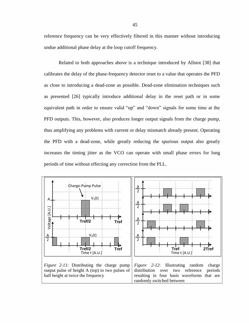
45
reference frequency can be very effectively filtered in this manner without introducing
undue additional phase delay at the loop cutoff frequency.
Related to both approaches above is a technique introduced by Allstot [38] that
calibrates the delay of the phase-frequency detector reset to a value that operates the PFD
as close to introducing a dead-zone as possible. Dead-zone elimination techniques such
as presented [26] typically introduce additional delay in the reset path or in some
equivalent path in order to ensure valid “up” and “down” signals for some time at the
PFD outputs. This, however, also produces longer output signals from the charge pump,
thus amplifying any problems with current or delay mismatch already present. Operating
the PFD with a dead-zone, while greatly reducing the spurious output also greatly
increases the timing jitter as the VCO can operate with small phase errors for long
periods of time without effecting any correction from the PLL.
Figure 2-11: Distributing the charge pump
output pulse of height A (top) to two pulses of
half height at twice the frequency
Figure 2-12: Illustrating random charge
distribution over two reference periods
resulting in four basis waveforms that are
randomly switched between
Time t [A.U.]
Vo
ltag
e [A
.U.]
Tref
Charge-Pump Pulse
A
Tref/2
Tref/2 Tref
A2
V1(t)
V2(t)
Time t [A.U.]Tref 2Tref
A2
A2
A2
A2
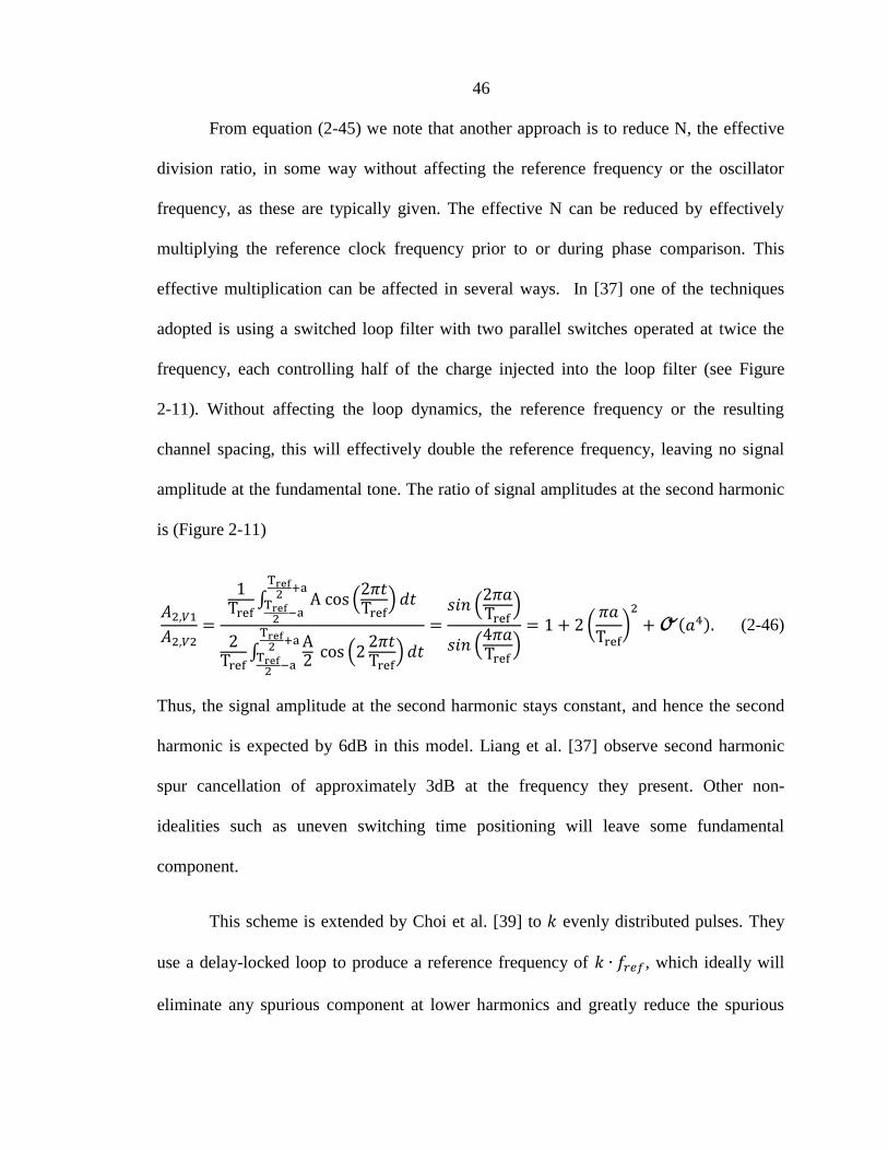
46
From equation (2-45) we note that another approach is to reduce N, the effective
division ratio, in some way without affecting the reference frequency or the oscillator
frequency, as these are typically given. The effective N can be reduced by effectively
multiplying the reference clock frequency prior to or during phase comparison. This
effective multiplication can be affected in several ways. In [37] one of the techniques
adopted is using a switched loop filter with two parallel switches operated at twice the
frequency, each controlling half of the charge injected into the loop filter (see Figure
2-11). Without affecting the loop dynamics, the reference frequency or the resulting
channel spacing, this will effectively double the reference frequency, leaving no signal
amplitude at the fundamental tone. The ratio of signal amplitudes at the second harmonic
is (Figure 2-11)
∫ (
)
∫ (
)
(
)
(
) (
)
( ) (2-46)
Thus, the signal amplitude at the second harmonic stays constant, and hence the second
harmonic is expected by 6dB in this model. Liang et al. [37] observe second harmonic
spur cancellation of approximately 3dB at the frequency they present. Other non-
idealities such as uneven switching time positioning will leave some fundamental
component.
This scheme is extended by Choi et al. [39] to evenly distributed pulses. They
use a delay-locked loop to produce a reference frequency of , which ideally will
eliminate any spurious component at lower harmonics and greatly reduce the spurious

47
output at the harmonic. The price is an implementation of an additional delay
locked loop, which consumes an additional 20% of the power and area. Even though
these techniques are claimed as novel, multiplication of the reference frequency is not a
new idea and is included in any general analysis for phase-locked loops (e.g., see [32]).
However, it does introduce an additional degree of freedom, particularly when a low
reference frequency has to be used. As for the noise impact, neither author discusses it,
but we expect little impact as the reference frequency is effectively up-converted,
increasing its noise by ( ) with a corresponding reduced penalty in the PLL since
the noise is ( ⁄ ) that of the reference in-band.
Another idea to reduce spurious components is based on dithering by distributing
the charge pump charge quasi-randomly within the reference clock cycle. Those in [37]
use a technique of placing the charge randomly at one out of two places (separated by one
half the reference period) using a PBRS to generate a quasi-random bit stream. This
technique reduces the overall spurious tone level by distributing the power to higher
harmonics as well as spreading it to intermediate frequencies (compare Figure 2-12 for
illustration). Some analysis based on unit impulses is done here [40]. The power does not
contain energy around DC, and thus the spreading does not affect the close-in phase
noise.
To summarize, the above techniques fall into several broad categories: (1)
techniques improving the performance of the individual circuit blocks (PFD, charge
pump, loop filter) involved (2) Techniques involving reducing the VCO gain of the loop
in lock, using either switched filters with lock detectors or multi-path approaches, (3)

48
techniques based on multiplying the effective reference frequency and (4) techniques
based on noise spreading.
All of the above techniques share a few things in common: with the exception of
techniques that affect the VCO gain, all of the above techniques mitigate the spur by
reducing the control voltage ripple to a minimum, spreading the power to higher
frequency or to dither the power across frequencies. In effect then, the techniques do not
address spurious tones produced by supply or substrate feed-through. The techniques
lowering VCO gain bring in new issues, most notably loop stability and noise, but do also
mitigate spurious content produced by supply and substrate feed-through since lowering
the VCO gain typically lowers the VCO’s AM-PM conversion as well. Edge
interpolation techniques require re-synthesis of a higher clock without introducing delay
errors. In effect, such techniques require an additional delay-locked loop, transferring the
superior spurious tone performance of the delay locked loop to the phase-locked loop.
But most notably, none of the techniques reduce the spurious tone output using a closed-
loop feedback approach, which will be introduced in the next section.
Section 2.3.5 – A System-Level Closed-Loop Feedback Approach
Spurious tones can be significantly reduced using the above approaches, but any
open-loop technique will result in some residual spurious output because the circuits
involved are operating from a periodic reference clock. The most effective techniques are
sampling the loop filter, as it reduces any non-ideal and transient effects of prior circuitry
to a single charge-transfer mechanism. Any remaining reduction efforts can then

49
concentrate on minimizing charge feed-through through the loop filter switch as well as
reducing supply and substrate bounce.
Using any of the approaches, however, will lead to some residual spurious
component that can vary over process, temperature and operating voltage, and no open-
loop technique can fully cancel the spurious components of any periodically operating
phase-locked loop.
In our work, we investigated a truly closed-loop technique that senses the
spurious content of the VCO using the control voltage disturbance as a proxy. Active
injection of small pulse-type waveforms is used to actively produce spurious output that
counteracts the spurious output produced by the PLL. Our technique is general in that it
can be operated either by itself or in parallel with other techniques previously presented.
Figure 2-13 illustrates our approach conceptually. In order to sense the spurious
output of the PLL, the VCO control voltage is digitally sampled and the samples are
Figure 2-13: Conceptual illustration of the
system-level closed-loop approach adopted.
Figure 2-14: Block Diagram of the
implemented system
S++ VCO
Uncorrected VCO control
voltage
time
Vo
lta
ge
0Tref
Corrected, low-ripple
control voltage waveform
Q-Pump H(s)
Vo
lta
ge
0 Tref
Added correction/spur
cancellation signal
time
Vo
lta
ge
0Tref
time
1
N
Sense
DSP Actuate
Q
AD
Q
AD
Q
AD
PFD
Charge pump/
loop filter
VCO
Off-chip crystal
reference
S
++
Detector
(synchronous
correlator)
Correction signal
generator
Digital closed-loop feedback
control
Harmonic Filter
DSP
ò
x4
Q
AD
A
D
Divider
state
Divider state
Divider state
1
N
50
processed in a DSP unit to reconstruct the control voltage waveform. The control voltage
waveform serves as a proxy for the produced spurious output, and the voltage sampled is
an amplified and band-pass filtered version of the control voltage referenced to the same
supply rail as the VCO supply. In this way, supply bounce producing spurious can be
taken into account as the control voltage bounce produces spurious output as a function
of the VCO supply rail voltages.
The timing for the control voltage samples is generated from the states of the
divider to divide the reference clock signal into N equally spaced time bins synchronous
to the control voltage and any perturbation. Because the perturbation of the control
voltage waveform and of the VCO itself is periodic, synchronously detecting the single
tones allows for almost arbitrary sensitivity as longer integration times can be used to
reduce the noise bandwidth similar to the operation of a lock-in amplifier or a spectrum
analyzer. Because the VCO edge zero-crossings vary in time when spurious tones are
present, using them to demodulate the FM signal directly is an alternative approach for
detecting the spurious output of the VCO as will be discussed in more detail in the
implementation section.
To inject an actuation signal, an error signal that consists of a series of timed
pulses with controllable amplitude is used. This approach was chosen for a variety of
reasons. First, the injected pulse waveform is similar in nature and shape to the waveform
that is attempted to be cancelled. In this manner, using even a few pulses, the total
spurious output power can be reduced more effectively as the power in several harmonics
is reduced simultaneously. Secondly, the circuit overhead becomes very small,
51
effectively consisting of a capacitor that can be charged to a programmable value and
whose charge is transferred at a programmable time instance to a loop filter. Thirdly, this
approach is scalable, as several of these channels can be operated in parallel. An
alternative approach could use single tone injections, where an arbitrary waveform is
synthesized from (mostly) pure tones of the reference frequency and its harmonics. The
difficulty with such an approach is that it requires generation of pure tones from a
reference clock that is typically in digital form. Furthermore, it requires this production
for all of the harmonics of interest. Our actuation circuit is more comparable to a poor
man’s direct digital waveform synthesizer.
Using N injected pulses of controllable amplitude and phase provides
degrees of freedom that can be used to control the amplitude and phases of the first
harmonics of the spurious tones produced. Higher frequency components are less
important, as additional filtering can be added to the loop filter removing the harmonics
more easily without unduly introducing phase-shift at the loop bandwidth, thus affecting
loop stability. Furthermore, because a tone at a higher harmonic but of the same strength
as a lower harmonic tone produces a lower spurious output as the effective FM
modulation index is lower.
A complete block diagram of the proposed frequency synthesizer is shown in
Figure 2-14. The control voltage is sampled using a subsampling correlator, and the time
samples are used to reconstruct the control voltage signal. The analog-to-digital
conversion is implemented off-chip in this test-chip, and the digital samples are read
through a GPIB interface by a MATLAB program, which acts as a DSP end. The

52
program also generates programming values to control the timing and amplitude of the
generated pulses in the correction signal generator, as well as programming the correlator
to sequentially take samples (also providing software DC offset cancellation). The
correction signal generator consists of four parallel channels of the programmable charge
pulse generator discussed above. The pulses are injected into the control voltage loop,
thus closing the feedback loop.
Figure 2-15: Detailed block diagram of the implemented PLL with all integrated components
Section 2.4 – Implementation
In this section, implementation details of the spurious tone cancellation PLL are
discussed. Each section discusses a particular block or subunit of the system. A detailed
block diagram of the integrated PLL components is depicted in Figure 2-15. The VCO
(PL1) signal is divided by four using two static divide-by-two blocks (PL4). A dynamic
divider (PL5) provides channel selection. Its output is retimed to lower the noise floor. A
DQ
PFD
2
2
N
fLO1
fLO2
x2
PL1
PL2PL3
PL4
PL4
PL5
PS1
PC1Divider state
Divider state
PL6
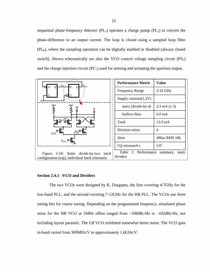
53
sequential phase-frequency detector (PL3) operates a charge pump (PL2) to convert the
phase-difference to an output current. The loop is closed using a sampled loop filter
(PL6), where the sampling operation can be digitally enabled or disabled (always closed
switch). Shown schematically are also the VCO control voltage sampling circuit (PS1)
and the charge injection circuit (PC1) used for sensing and actuating the spurious output.
Figure 2-16: Static divide-by-two latch
configuration (top), individual latch schematic
Performance Metric Value
Frequency Range 2-16 GHz
Supply currents(1.2V)
static (divide-by-4) 2.3 mA (x 3)
buffers+bias 6.0 mA
Total 12.9 mA
Division ratios 4
Jitter 490as RMS 10k
I/Q mismatch s 3.6o
Table 1: Performance summary, static
dividers
Section 2.4.1 –VCO and Dividers
The two VCOs were designed by K. Dasgupta, the first covering 4-7GHz for the
low-band PLL, and the second covering 7-12GHz for the HB PLL. The VCOs use three
tuning bits for coarse tuning. Depending on the programmed frequency, simulated phase
noise for the HB VCO at 1MHz offset ranged from –108dBc/Hz to –102dBc/Hz, not
including layout parasitic. The LB VCO exhibited somewhat better noise. The VCO gain
in-band varied from 300MHz/V to approximately 1.6GHz/V.
CLKCLK
Din Din
D
C
Q QD
C
Iout Qout
Q Q
Vbias
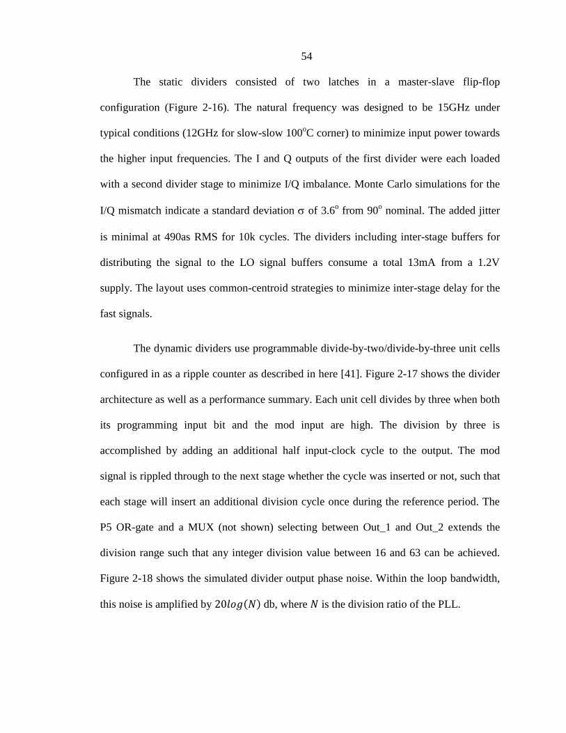
54
The static dividers consisted of two latches in a master-slave flip-flop
configuration (Figure 2-16). The natural frequency was designed to be 15GHz under
typical conditions (12GHz for slow-slow 100oC corner) to minimize input power towards
the higher input frequencies. The I and Q outputs of the first divider were each loaded
with a second divider stage to minimize I/Q imbalance. Monte Carlo simulations for the
I/Q mismatch indicate a standard deviation of 3.6o from 90
o nominal. The added jitter
is minimal at 490as RMS for 10k cycles. The dividers including inter-stage buffers for
distributing the signal to the LO signal buffers consume a total 13mA from a 1.2V
supply. The layout uses common-centroid strategies to minimize inter-stage delay for the
fast signals.
The dynamic dividers use programmable divide-by-two/divide-by-three unit cells
configured in as a ripple counter as described in here [41]. Figure 2-17 shows the divider
architecture as well as a performance summary. Each unit cell divides by three when both
its programming input bit and the mod input are high. The division by three is
accomplished by adding an additional half input-clock cycle to the output. The mod
signal is rippled through to the next stage whether the cycle was inserted or not, such that
each stage will insert an additional division cycle once during the reference period. The
P5 OR-gate and a MUX (not shown) selecting between Out_1 and Out_2 extends the
division range such that any integer division value between 16 and 63 can be achieved.
Figure 2-18 shows the simulated divider output phase noise. Within the loop bandwidth,
this noise is amplified by ( ) db, where is the division ratio of the PLL.

55
Figure 2-17: Dynamic divider architecture
and performance summary.
Figure 2-18: Simulated dynamic divider
output phase noise.
Section 2.4.2 –Phase-Frequency Detector, Charge Pump and Loop filter
The phase-frequency detector (PFD), charge pump (CP) and loop filter (LF)
designs are discussed next. The PFD consists of a set of set/reset latches enabling “up”
and “down” outputs whenever the reference edge or the divider edge rises, respectively,
and resetting when the other edge rises. Additional circuitry translates the output voltage
level from 1.2V to 2.5V as required by the charge pump. A dead-zone elimination circuit
waits until both outputs are valid high at the charge pump before lowering the outputs.
This is done independently of the R/S pair resetting in order to ensure that all edges are
captured. Figure 2-19 shows a block diagram of the PFD in addition to a performance
summary for the detection blocks comprising the PFD, CP and the loop filter. The
simulated output phase noise of the phase-frequency detector is shown in Figure 2-20.
The PFD phase noise is 12dB higher than the divider noise, and thus dominates the close-
in phase noise performance of the PLL. The PFD phase noise contributions originate
from several blocks, with the voltage converters and the dead-zone elimination circuits
State outputs
C Q
mod
2/3Q
mod
2/3C Q
mod
2/3C Q
mod
2/3C Q
mod
2/3C
P0 P1 P2 P3 P4P5
in Out_1Out_2
Performance Summary:
Division Steps : 16 – 63
Current (1.2V) : 14mA
Speed : >7GHz
RMS Jitter : 157 fs
-170
-160
-150
-140
-130
-120
1.E+02 1.E+03 1.E+04 1.E+05 1.E+06 1.E+07
Ph
ase
No
ise
[dB
c/H
z]
Offset Frequency [Hz]
Static Divider Simulated Phase Noise
tt50
ss100

56
contributing significantly. The total PFD RMS jitter is 280fs, dominating the jitter
contributed by the divider [42].
Figure 2-19: PFD block diagram;
performance summary of PFD, CP and loop
filter blocks.
Figure 2-20: Simulated phase noise PFD
(blue); contributions of PFD (green), loop
filter (red) to PLL noise, and sum total
(black).
The loop filter component values and charge pump current were selected next,
based on the noise contribution and passive component sizing. A loop filter capacitance
of around 250pF was deemed the maximum possible in terms of available area, and a
loop filter bandwidth of around 1MHz was targeted based on a similar value in the
AMRFC reference design. Additionally, voltage overhead requirements during
acquisition were taken into consideration such that a minimum size of the parallel
capacitor was required for a given charge pump current. A minimum attenuation of 5dB
at 50MHz for the additional LPF section was also required, as well as a maximum jitter
peaking of 3dB across the band, taking into account the different loop response at the
lowest, highest and an intermediate frequency. All of these constraints were added to a
R
S Q
S
R
Q
R
S
Q
1.2V
2.5V
1.2V
2.5V
1.2V
2.5V
2.5V
1.2V
Reset
Reset
ref
divdown
up
Performance Summary (PFD, CP, LF):
Reference Frequency : 50 MHz
Charge Pump Current : 400uA
Loop Bandwidth : 1 MHz
PFD RMS jitter : 280 fs
Loop Filter jitter : 239 fs
1.2V Supply Current : 2.4 mA
2.5V Supply Current : 7.2 mA
-170
-160
-150
-140
-130
-120
-110
-100
-90
-80
-70
1.E+02 1.E+03 1.E+04 1.E+05 1.E+06 1.E+07
Ph
ase
No
ise
[d
Bc/
Hz]
Offset Frequency [Hz]
PFD, Loop Filter Simulated Phase Noise
PFD, tt50LFPFD, shapedTotal
57
linear PLL model that calculated noise contribution from the loop filter, and loop filter
and charge pump current values were determined from a minimization like that of output
noise, with additional judicious considerations of different constraint scenarios. As can be
seen from Figure 2-20, the loop filter noise dominates the PLL phase noise performance
past a 200 kHz offset frequency, being also larger than the VCO noise. The remedy
would have been a selection of a larger charge pump current (ideally 1.5mA to 2mA), but
at the expense of loop filter size that was considered prohibitively large.
With the charge pump current determined, the charge pump using a pair of
cascoded current mirrors with pass-switches, and an opamp servo to set the replica arm
voltage to the charge pump output voltage to minimize charge feed-through. Figure 2-21
shows a schematic. Not shown is an additional servo that regulates the PMOS upper
mirror to set midpoint of the mirror arm to the charge pump output voltage DC.4 The
charge pump is balanced (no reference output produced) at 1V output in simulation.
Biasing details are not shown in Figure 2-21.
4 This additional servo was found to not affect the reference tone produced by the charge pump both in
simulation as well as measurement.

58
Figure 2-21: Charge pump schematic.
Figure 2-22: Sampling detector block
diagram, and input amplifier circuit detail.
Section 2.4.3 – Sampling Correlator Detector
We next discuss the design of the sampling correlator. A block diagram is shown
in Figure 2-22. The correlator is AC coupled to the control voltage, sharing a supply with
the VCO such that the AC ripple is referenced to the supply rails in a ratio yielding a
good approximation of the translation of ripple w.r.t. to each supply in the VCO to VCO
output spurs. A single-ended-to-differential conversion is performed using a DC servo
loop around the input amplification stages such that the output has no DC offset with a
loop bandwidth well below the reference frequency. The initial single-ended-to-
differential conversion uses a series of inverters, self-biased in one branch and servo-
biased in the other, as the delay introduced at the reference frequency and the relevant
harmonics is low enough to produce a quasi-differential signal. Further differential
amplification reduces common mode output to a minimum.
dn Ibiasdn
up up
+-
To loop filter
Q
S
R
Control
voltage
Divider state
Switching
Mixer
Low-pass
filter
Input
amplifiers
Output
bufferdisable
disable
Input amplifier chain
circuit detail VVDD,VCO
VIN
Voffset
VDD
Vout+ Vout-
VDD
Reset trigger
edge control
trigger
trigger
Set trigger
edge control
Detector
output
+
-
59
Low-pass filters with cutoff frequencies at several hundred MHz at the output of
the initial stages provide filtering necessary to minimize aliasing issues as well as
increasing the dynamic range, as the amplification stages can easily provide gain at
several GHz. A programming bit also allows switching between a low-gain and a high-
gain setting in case amplification of very weak signals is required (the low-gain setting is
the default setting). Gain and supply rejection versus frequency for both low- and high-
gain settings is shown in Figure 2-23. The input referred noise voltages in a 2MHz band
around 50MHz, 100MHz and 400MHz are 2.5uV, 2.1uV and 2.0uV RMS, respectively,
allowing integration times of a microsecond in order to detect spurious tone amplitudes
of 10uV.
The input amplifier is followed by a product detector, a Gilbert Cell style current
steering mixer. The LO waveform is generated by a set-reset flip flop with the set and
reset edges selected from the divider state transitions. In this way, the detector can be
programmed to integrate the (amplified) control voltage signal over programmable time
windows within the reference clock cycle. The product detector output is a DC sample
value that is further amplified. The integration time constant is set by on-chip capacitors
to approximately 1us, but can be increased by averaging multiple, uncorrelated samples.
A transient noise simulation is performed with a 10uV sine wave input
(corresponding to a spurious output of approximately -66dBc) can be barely detected
with a single sample. However, using multiple samples, the signal-to-noise ratio is
increased as the effective noise bandwidth is reduced.
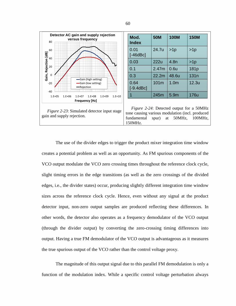
60
Figure 2-23: Simulated detector input stage
gain and supply rejection.
Figure 2-24: Detected output for a 50MHz
tone causing various modulation (incl. produced
fundamental spur) at 50MHz, 100MHz,
150MHz.
The use of the divider edges to trigger the product mixer integration time window
creates a potential problem as well as an opportunity. As FM spurious components of the
VCO output modulate the VCO zero crossing times throughout the reference clock cycle,
slight timing errors in the edge transitions (as well as the zero crossings of the divided
edges, i.e., the divider states) occur, producing slightly different integration time window
sizes across the reference clock cycle. Hence, even without any signal at the product
detector input, non-zero output samples are produced reflecting these differences. In
other words, the detector also operates as a frequency demodulator of the VCO output
(through the divider output) by converting the zero-crossing timing differences into
output. Having a true FM demodulator of the VCO output is advantageous as it measures
the true spurious output of the VCO rather than the control voltage proxy.
The magnitude of this output signal due to this parallel FM demodulation is only a
function of the modulation index. While a specific control voltage perturbation always
-40
-20
0
20
40
60
80
1.E+05 1.E+06 1.E+07 1.E+08 1.E+09 1.E+10
Gai
n, R
eje
ctio
n [
dB
]
Frequency [Hz]
Gain (high setting)
Gain (low setting)
Rejection
Detector AC gain and supply rejection versus frequency Mod.
Index
50M 100M 150M
0.01
[-46dBc]
24.7u >1p >1p
0.03 222u 4.8n >1p
0.1 2.47m 0.6u 181p
0.3 22.2m 48.6u 131n
0.64
[-9.4dBc]
101m 1.0m 12.3u
1 245m 5.9m 176u

61
produces the same detector output for a given input amplification, the timing errors (FM
modulation) are a function of the VCO gain alone. Using the particular values of VCO
gain, center frequency, spur amplitude and input amplifier gain, the output amplitudes
produced by this FM modulation were calculated, but found to be two orders of
magnitude lower than the primary output produced by the corresponding control voltage
perturbations. The results (including mixing products detected at very large spurious
signals) are summarized in Figure 2-24.
The detection circuit is extended to include a programmable option to short the
product detector input such that only the output due to FM demodulation of the divider-
state-signal is detected. Additional base-band stages are added to provide stronger signal
amplification (with digital gain control). That is the function of the disable switch at the
detector input as shown in Figure 2-22.
Figure 2-25: Spur tone actuation circuit
block diagram
Figure 2-26: Injected tone strength for first
four harmonics.
control
Digital trigger
AD
Vbias
wordcontrol
Trigger
delay fine-
tune
word
Divide-
by-N
VCO
control
voltage
Programmable
correction signal
generation circuit
statedivider
control
Digital trigger
AD
Vbias
wordcontrol
Trigger
delay fine-
tune
word
control
Digital trigger
AD
Vbias
wordcontrol
Trigger
delay fine-
tune
word
control
Digital trigger
AD
Vbias
wordcontrol
Trigger
delay fine-
tune
word
Digital control
Digital control
x 4
0
200
400
600
800
1000
1200
1400
1600
1800
0 50 100 150 200 250
Inje
cte
d v
olt
age
mag
nit
ud
e [
uV
]
Programming value [8 bits]
Injected Spur Magnitude
50M
100M
150M
200M

62
Section 2.4.4 – Spurious Tone Actuator
The spurious tone actuation circuit (error signal generator) implemented consists
of four parallel channels of charge injection circuitry. A block diagram of an individual
channel is shown in Figure 2-25. For each channel, a programmable amount of charge
can be injected into the control voltage node at a programmable time-instant during the
reference clock cycle. The charge is injected into the control voltage node periodically by
closing a switch once during a reference clock cycle. With four channels, four
independently controllable injections can be made during each reference clock cycle. The
trigger for the switch is generated by first comparing the divider state to a programmable
known state, generating a trigger signal at a state transition point of the divider. A
programmable, current-starved delay cell provides additional timing control. The four
parallel channels can generate a waveform synchronous to the control voltage waveform,
allowing up to eight degrees of freedom.
For a targeted minimum output spurious tone level of -70dBc, we can calculate
the voltage amplitude disturbance on the control voltage line to be
(2-47)
for N=240, , and .
Assuming two sine signals of amplitude and phase-difference are subtracted,
the resulting sinusoid has an amplitude of ( ⁄ ). For , we require a
phase accuracy of 5.7o to reduce a -50dBc spur to a -70dBc spur, then.
63
The signal injected closely resembles a short pulse in simulation. The holding
capacitor size is chosen to ensure recharging during a reference clock cycle given the
D/A output current, and the series decoupling capacitor size is chosen to produce a
desired range of output amplitudes at the control voltage. The D/A provides eight bits of
control. Shown in Figure 2-26 are the magnitudes of the first four error signal harmonics
for various bit settings. The magnitudes drop somewhat as the harmonic number
increases as expected for pulses of finite time duration. The step size is approximately
nine microvolt around the zero point, sufficient to provide reduction of spurious output
tones below -50dBc as shown above.
The charge holding capacitor value is 3pF, thus generating an RMS noise voltage
of 37uV. The voltage placed onto the loop filter, however, is itself divided by a factor of
approximately one thousand, thus, the effective RMS noise injected is on the order of
tens of nanovolt and the effective floor for the spurious tone reduction is on the order of –
100dBc for this circuit.
Because the error signal generator runs continuously, reducing its current
consumption will greatly reduce the overall overhead required for the spurious tone
correction capability. In this implementation, the majority of the current is consumed by
the digital-to-analog converter, as a single design was used for the various D/A
implementations on the HEALICs receiver. The design used consumes several milli-
amperes, with reductions easily possible particularly because non-linearity is not an issue.
Secondly, the divider state used is a buffered version of the divider state routed across
hundreds of micron. In order to ensure sufficient signal strength, the buffer amplifiers
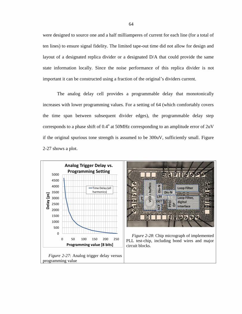
64
were designed to source one and a half milliamperes of current for each line (for a total of
ten lines) to ensure signal fidelity. The limited tape-out time did not allow for design and
layout of a designated replica divider or a designated D/A that could provide the same
state information locally. Since the noise performance of this replica divider is not
important it can be constructed using a fraction of the original’s dividers current.
The analog delay cell provides a programmable delay that monotonically
increases with lower programming values. For a setting of 64 (which comfortably covers
the time span between subsequent divider edges), the programmable delay step
corresponds to a phase shift of 0.4o at 50MHz corresponding to an amplitude error of 2uV
if the original spurious tone strength is assumed to be 300uV, sufficiently small. Figure
2-27 shows a plot.
Figure 2-27: Analog trigger delay versus
programming value
Figure 2-28: Chip micrograph of implemented
PLL test-chip, including bond wires and major
circuit blocks.
0
500
1000
1500
2000
2500
3000
3500
4000
4500
5000
0 50 100 150 200 250
Del
ay [
ps]
Programming value [8 bits]
Analog Trigger Delay vs. Programming Setting
Time Delay (all harmonics)
65
Section 2.4.5 – System Integration and Closed-Loop Control
The implemented PLL core itself uses a 50MHz off-chip reference signal, and can
be tuned from 7-12GHz. The overall PLL loop bandwidth is 800 kHz-1.2 MHz,
depending on the operation frequency. Including switched capacitor banks for coarse
tuning control, the VCO gain kvco is 2GHz/V typically for midrange control voltages. The
divide-by-N circuit generates N distinguishable states used for providing timing
information to generate programmable trigger signals in the detector and correction
signal generator. The PLL loop is closed with a charge pump and a third order loop filter
as previously discussed.
The PLLs are part of a larger, self-healing receiver system, but test-chip cut-outs
were taped out to test the PLL subsystem. A chip photograph is shown in Figure 2-28.
The chip contains ten-bit-wide, addressable digital registers that control, among
others, the injected pulse strength and timing as well as the correlation time window. The
detector output is an analog voltage that is converted in an off-chip ADC to a digital
signal that can be read out over a USB interface by MATLAB. The USB interface also
controls the programming of the integrated circuit (such as the injected pulse timing and
amplitude). The digital feedback loop is closed through this interface in MATLAB for
testing purposes.
The control voltage waveform is reconstructed by sampling the control voltage
waveform over successive time windows within the reference clock period cycle. The
correlator time window rising and falling edges are set to times close to half a reference
period clock cycle apart in order to minimize additional DC offsets in the signal. By

66
taking the difference between two such measurements where only one of the edge
timings changes, a sample in the changing time window can be taken. Additionally, any
static errors in the reading are eliminated by repeating the measurement with swapped
rising and falling timing edge windows. Thus, for each sample, four measurements are
performed. In order to reconstruct a signal waveform, a minimum of sixteen windows are
chosen within the reference clock cycle. The number of available windows varies with
the division ratio N. The window can be triggered by every fourth VCO signal transition
in the lower VCO frequency range, and every eighth otherwise.
Figure 2-29: Signal power versus test-pulse
injected timing
Figure 2-30: Signal power versus test-pulse
amplitude around an extremum.
From the reconstructed signal waveform, the total spurious tone output power is
calculated, appropriately weighing the different harmonic components. The control
feedback algorithm minimizes this power, using the following algorithm: A test-pulse of
small but finite strength is injected at fixed timing offsets within the reference clock
period using the first channel. The total output power is measured and recorded, resulting
in a graph of spurious tone power versus injected signal timing as illustrated in Figure
Pulse Injection time t [A.U.]
Co
ntr
ol V
olt
age
Sign
al P
ow
er [
A.U
.]
Tref
Local extrema in timing explored by gradient search
Pulse Amplitude
Co
ntr
ol V
olt
age
Sign
al P
ow
er [
A.U
.]Min power for pulse injected at
position n

67
2-29. Around the extrema, additional fine-tuning information is gained using the analog
delay in the pulse injection circuit. Since the phase and amplitude of the pulse are
potentially non-optimal, each of these extrema is a potential global minimum. Thus, for
each of these extrema (i.e., timing points), the correct amplitude is determined via a
gradient descent (algorithmically by successive binary triangulation). Compare Figure
2-30 for an illustration. Each of the resulting minima power values are recorded in
memory and the absolute minimum is chosen. Thus, for the first channel and injection
pulse timing and amplitude is determined. With this new injection in place, the second,
third, etc., channel programming settings are determined.
Figure 2-31: Simulated spurious tone
reduction using four harmonics and eight
channels for ten different, random scenarios
Figure 2-32: Same for 16 harmonics and 32
pulses.
To evaluate this algorithm, a MATLAB program is written that generates a
random waveform containing harmonics and injection channels. The injected
0 50 100-100
-80
-60
-40
-20
0
Iteration
Tota
l P
ow
er
Reduction [
dB
]
Spur Power Reduction vs Iteration,
4 harmonics, 8 pulses
0 50 100-50
-40
-30
-20
-10
0
Spur Power Reduction vs Iteration,
16 harmonics, 32 pulses
Iteration
Tota
l P
ow
er
Reduction [
dB
]
68
waveform is a different random waveform containing harmonics as well, and the above
algorithm is implemented. The results of ten such runs for a total of four and sixteen
harmonics are shown in Figure 2-31 and Figure 2-32, respectively.
Section 2.5 – Experimental Results
In this section, we will describe experimental results, proving the concept of
closed-loop spurious tone cancellation developed in this chapter. The PLL is
implemented in a low-power 65nm CMOS process. Test-chip dimensions are 1.4mm x
0.9mm, with 150um x 50um and 130u x 80u um used by the detection and correction
signal circuits, respectively. The test-chip is wire-bonded to a 28-pin PLCC, and the
buffered VCO output signal is probed from pads directly. The PLCC is large compared to
the die dimension, resulting in rather long bond-wires, and potential pick-up problems
through bond-wire coupling. A differential reference signal generated by an oven-
controlled crystal oscillator is provided through two SMA connections that are routed via
50 transmission lines and bond-wires to the reference signal input pads. Coupling
issues between these reference bond-wires and an adjacent supply line wire were noticed,
and the supply bond-wire was omitted (there were multiple available supply pads). A
photograph of the PCB with the test-chip and all wiring installed is shown in Figure 2-33.

69
Figure 2-33: Photograph of HEALICs PLL
PCB, mounted on probe station.
Figure 2-34: PLL test-setup overview
In order to eliminate amplitude modulation present on the VCO output, the VCO
output is divided-by-two using a Centellax frequency divider. This will strip amplitude
modulated signal sideband spurs from the measured signal, as well as attenuate the
spurious side-tone strength by 6dB. For all results shown, 6dB has been added to the
sideband spurs to show the original spurious tone strength.
The chip contains two supply domains (1.2V and 2.5V), which are each supplied
by on-PCB supply regulators. These regulators can be bypassed since they add noise to
the output signal. A ten-wire custom-made flat cable connects the PCB to a test
motherboard. The motherboard contains a 16-bit ADC and a Xilinx FPGA. The FPGA
can generate the correct programming signals and addresses for the integrated shift
registers, as well as prepare a read-out of the ADC. It also incorporates a USB interface,
such that commands can be sent via USB from a workstation PC to the motherboard,
which in turn control the interface to the test-chip. While the interface is slow (each
Workstation PCTesting
Motherboard
Programming
commands
Detector
readout
PLL PCB
Detector
voltage
Programming
commands
signals
50 MHz crystal
reference
Supplies
VCO output
Centellax div-
by-two
Spectrum
Analyzer

70
command requires about half a second to be executed), it allows programming and testing
a high-level testing interface in MATLAB.
Initial testing of the PLL without the self-healing aspect is performed. The PLL
frequency output spans 7.4GHz to 12.4GHz using a 50MHz reference signal, slightly
higher than designed. The phase noise at 1MHz offset is about -100dBc, depending on
the programmed frequency. Activation of the elimination circuit has no measureable
impact on broadband phase noise. The PLL consumes 138mW including 50 drivers for
the VCO and the VCO-divide-by-2 outputs. Assuming an in-situ duty cycle of 0.1%, the
detection circuit consumes 16uW when operated. The digital back-end can be run on a
similar duty cycle. The elimination circuit core consumes approximately 5mW, with
further reduction possible.
A severe programming issue was identified due to a faulty implementation5 of the
digital shift registers that resulted in random variations in programmability across
different chips. The fault occurs due to the use of a single set of latches clocked from the
same clock, resulting in local clock race issues. Because the shift-registers are triple-
welled and the different registers may incur different threshold voltages, local clock race
issues are exacerbated when slow-rising clock-edges are only available. As a result,
among eight different chips tested, only one had a sufficient number of working registers
to be testable. The number of testable registers includes all frequency programming
registers and two out of four injection channels. Most other tested chips would fail to be
programmable for all operating frequencies.
5 This fault is common to all the test-chips implemented as part of this program since the shift register
design/layout is shared among all designers, similar to common ESD design also shared for this project.

71
Because the PLL test-chip had an integrated Schmitt trigger to locally reject clock
ringing, little could be done to increase the slope of the clock edges (potentially
alleviating race issues) off-chip. A focused ion-beam bypass was performed on one chip,
but the chip was un-programmable after the procedure. For these reasons, the reported
results include two injection channels. Because of the Schmitt-trigger, a “trick”, which
involves substantially reducing the digital supply voltage to slow the register speed down
substantially, was also not available.6
The test setup used for all measurements is shown schematically in Figure 2-34. A
photograph is shown in Figure 2-35.
6 This is how several of the other test-chips were programmed with a little more success (but still with
issues in the case of the large main receiver chip).
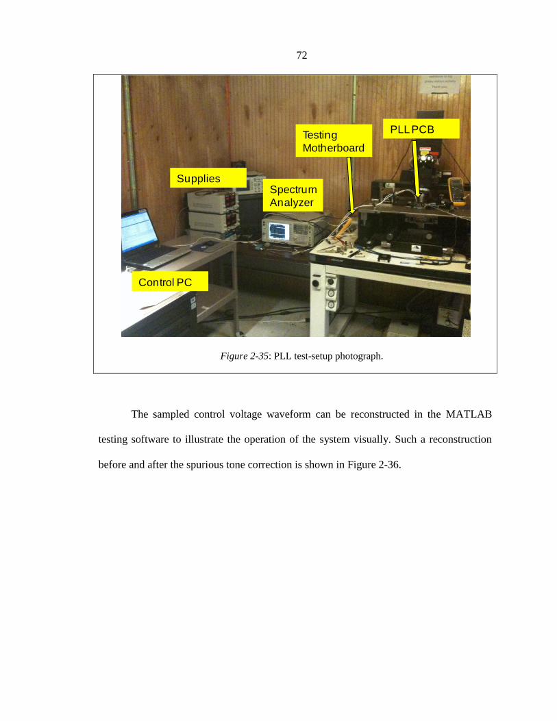
72
Figure 2-35: PLL test-setup photograph.
The sampled control voltage waveform can be reconstructed in the MATLAB
testing software to illustrate the operation of the system visually. Such a reconstruction
before and after the spurious tone correction is shown in Figure 2-36.
Spectrum
Analyzer
Testing
Motherboard
PLL PCB
Supplies
Control PC
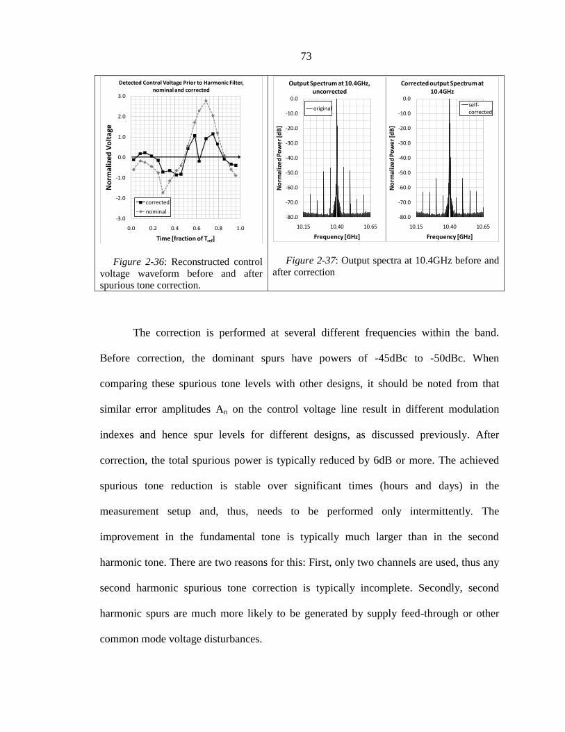
73
Figure 2-36: Reconstructed control
voltage waveform before and after
spurious tone correction.
Figure 2-37: Output spectra at 10.4GHz before and
after correction
The correction is performed at several different frequencies within the band.
Before correction, the dominant spurs have powers of -45dBc to -50dBc. When
comparing these spurious tone levels with other designs, it should be noted from that
similar error amplitudes An on the control voltage line result in different modulation
indexes and hence spur levels for different designs, as discussed previously. After
correction, the total spurious power is typically reduced by 6dB or more. The achieved
spurious tone reduction is stable over significant times (hours and days) in the
measurement setup and, thus, needs to be performed only intermittently. The
improvement in the fundamental tone is typically much larger than in the second
harmonic tone. There are two reasons for this: First, only two channels are used, thus any
second harmonic spurious tone correction is typically incomplete. Secondly, second
harmonic spurs are much more likely to be generated by supply feed-through or other
common mode voltage disturbances.
-3.0
-2.0
-1.0
0.0
1.0
2.0
3.0
0.0 0.2 0.4 0.6 0.8 1.0
No
rmal
ize
d V
olt
age
Time [fraction of Tref]
Detected Control Voltage Prior to Harmonic Filter, nominal and corrected
corrected
nominal-80.0
-70.0
-60.0
-50.0
-40.0
-30.0
-20.0
-10.0
0.0
10.15 10.40 10.65
No
rmal
ize
d P
ow
er
[dB
]
Frequency [GHz]
Corrected output Spectrum at 10.4GHz
self-corrected
-80.0
-70.0
-60.0
-50.0
-40.0
-30.0
-20.0
-10.0
0.0
10.15 10.40 10.65
No
rmal
ize
d P
ow
er
[dB
]
Frequency [GHz]
Output Spectrum at 10.4GHz, uncorrected
original
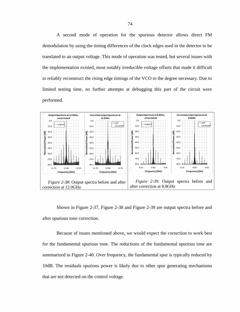
74
A second mode of operation for the spurious detector allows direct FM
demodulation by using the timing differences of the clock edges used in the detector to be
translated to an output voltage. This mode of operation was tested, but several issues with
the implementation existed, most notably irreducible voltage offsets that made it difficult
to reliably reconstruct the rising edge timings of the VCO to the degree necessary. Due to
limited testing time, no further attempts at debugging this part of the circuit were
performed.
Figure 2-38: Output spectra before and after
correction at 12.0GHz
Figure 2-39: Output spectra before and
after correction at 8.8GHz
Shown in Figure 2-37, Figure 2-38 and Figure 2-39 are output spectra before and
after spurious tone correction.
Because of issues mentioned above, we would expect the correction to work best
for the fundamental spurious tone. The reductions of the fundamental spurious tone are
summarized in Figure 2-40. Over frequency, the fundamental spur is typically reduced by
10dB. The residuals spurious power is likely due to other spur generating mechanisms
that are not detected on the control voltage.
-80.0
-70.0
-60.0
-50.0
-40.0
-30.0
-20.0
-10.0
0.0
11.75 12.00 12.25
No
rmal
ize
d P
ow
er
[dB
]
Frequency [GHz]
Output Spectrum at 12.0GHz, uncorrected
original
-80.0
-70.0
-60.0
-50.0
-40.0
-30.0
-20.0
-10.0
0.0
11.75 12.00 12.25
No
rmal
ize
d P
ow
er
[dB
]
Frequency [GHz]
Corrected output Spectrum at 12.0GHz
self-corrected
-80.0
-70.0
-60.0
-50.0
-40.0
-30.0
-20.0
-10.0
0.0
8.55 8.80 9.05
No
rmal
ize
d P
ow
er
[dB
]
Frequency [GHz]
Output Spectrum at 8.8GHz, uncorrected
original
-80.0
-70.0
-60.0
-50.0
-40.0
-30.0
-20.0
-10.0
0.0
8.55 8.80 9.05
No
rmal
ize
d P
ow
er
[dB
]Frequency [GHz]
Corrected output Spectrum at 8.8GHz
self-corrected
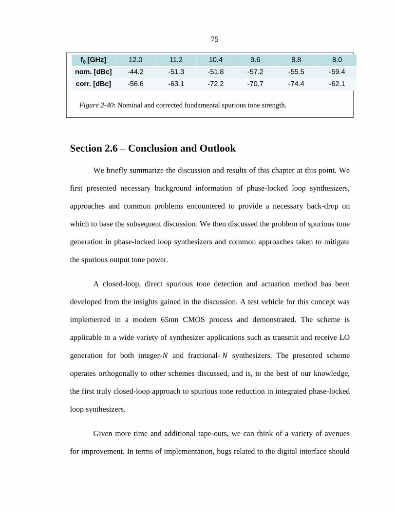
75
Figure 2-40: Nominal and corrected fundamental spurious tone strength.
Section 2.6 – Conclusion and Outlook
We briefly summarize the discussion and results of this chapter at this point. We
first presented necessary background information of phase-locked loop synthesizers,
approaches and common problems encountered to provide a necessary back-drop on
which to base the subsequent discussion. We then discussed the problem of spurious tone
generation in phase-locked loop synthesizers and common approaches taken to mitigate
the spurious output tone power.
A closed-loop, direct spurious tone detection and actuation method has been
developed from the insights gained in the discussion. A test vehicle for this concept was
implemented in a modern 65nm CMOS process and demonstrated. The scheme is
applicable to a wide variety of synthesizer applications such as transmit and receive LO
generation for both integer- and fractional- synthesizers. The presented scheme
operates orthogonally to other schemes discussed, and is, to the best of our knowledge,
the first truly closed-loop approach to spurious tone reduction in integrated phase-locked
loop synthesizers.
Given more time and additional tape-outs, we can think of a variety of avenues
for improvement. In terms of implementation, bugs related to the digital interface should
f0 [GHz] 12.0 11.2 10.4 9.6 8.8 8.0
nom. [dBc] -44.2 -51.3 -51.8 -57.2 -55.5 -59.4
corr. [dBc] -56.6 -63.1 -72.2 -70.7 -74.4 -62.1

76
obviously be removed to allow testing at the full four channel capacity. Secondly, a lot of
room for power reduction as well as area reduction exists. For power reduction, a local
divide-by- circuit should be used rather than routing the divider-state variables
globally. Furthermore, the on-chip DACs are very power-hungry, and their power
consumption can be reduced considerably. Thirdly, the injection circuit implementation
requires a standby charging current that could be reduced since the circuit’s noise
performance was overdesigned. Fourthly, the direct FM demodulation circuit could be
tested further, debugged if necessary and improved in a second tape-out to allow
correcting for supply feed-through and other issues. Finally, the feedback algorithm could
be implemented on an FPGA to perform the correction with the click of a button.
Since time and funding resources for this project were limited, several of the
above were thought about and planned for, but remain unrealized up to this date.

77
Chapter 3 – Techniques for Generation
and Detection of Signals beyond fmax
Section 3.1 – Introduction
Having discussed techniques for generating signals in the microwave region, the
focus will now shift towards a higher range of frequencies, in particular for frequencies
that lie above the maximum frequency at which the transistors provide linear gain.
Figure 3-1: Reproduced from [43], showing
cutoff frequency in modern CMOS devices
versus gate length.
Figure 3-2: Reproduced from [43],
showing technology node versus year of
production for Intel CMOS FETs.
Transistors in different technologies provide different maximum linear gain
frequencies , and the rapid advances in processing techniques and reduction in
minimum feature sizes in all technologies, but particularly in CMOS, have increased this
frequency for many devices over the years. As an example, Figure 3-1 and Figure 3-2
show the maximum linear current gain frequency for commercial CMOS technologies

78
(Intel, Co.) versus the year and the technology node, as reproduced from [43]; also
compare [44]. While GaAs and many other hetero-compound based devices offer
inherently higher mobilities and are thus inherently superior to silicon CMOS devices in
the same technology node, the far greater market for digital processing power compared
to extremely high-speed RF functionality has led to a proportionally larger investment in
CMOS based technologies compared to any of the silicon-based bipolar or compound
semiconductor based technologies in general. Therefore, the improvement in speed,
reliability and manufacturability of CMOS devices has been far greater compared to any
of the other mentioned technologies.
Furthermore, the availability of dense integrated circuitry in CMOS offers an
additional advantage for using CMOS based technologies even at very high frequencies,
as many integrated systems can greatly benefit from the availability of co-integrated
base-band and digital back ends.
This chapter serves to provide a background and context discussion for the
designs discussed in the following chapters. In this chapter, we will develop basic design
insights together with simulation and measurement results to put frequency conversion
designs of later chapters on a solid foundation.
Section 3.2 – Varactor- and Diode-based approaches in CMOS
In this section we will discuss high-frequency signal generation approaches that
use CMOS technologies based varactors and diodes. Approximate quantitative formulas
will be developed and compared to simulations and measurements.

79
Section 3.2.1 – Models for Varactor Up-conversion Efficiencies
In this subsection, we develop simple quantitative expressions for up-conversion
efficiencies of varactors.
Figure 3-3: MOS varactor-based frequency
up-conversion circuit (top) and model
(bottom).
Figure 3-4: Capacitance versus voltage
assumption made for circuit in Figure 3-3
Figure 3-3 shows an up-conversion circuit based on a MOS varactor. An input
current at the fundamental frequency flows into a varactor, here a non-linear MOS-based
capacitor. The conversion efficiency will be derived using the small-signal model shown
in Figure 3-3 (bottom).
In general, closed-form solutions cannot be obtained except when special
assumptions are used. For example, closed-form solutions are possible for an abrupt
junction frequency multiplier [45], but typically theoretical considerations are appended
by numerical simulations (e.g., see [46]) to predict other phenomena such as hysteresis or
in
I1
Iin
Cmin to Cmax
2in
Z2I2
Rs
Iin
in 2in
Z2
Voltage [V]
Cap
acit
ance
[F]
Cmin
Cmax

80
parasitic oscillations. The reader can also compare [47] for closed-form and numerical
solutions for classes of varactors with a ( ) ( ⁄ ) type non-
linearity.
For our discussion, we describe the capacitor non-linearity as a simple step-
function, which is a good approximation for CMOS FET gates. For the capacitance, we
make the simple assumption that it is given by
{
(3-1)
as shown in Figure 3-4. We assume that perfect harmonic filters limit the fundamental
current to flow between the input and the varactor, and the (second)-harmonic current
between varactor and output. We express the input current as ( ) ,
where is the fundamental frequency. We keep the charge moved into and out of the
varactor a constant, independent of frequency to keep the varactor voltage swing constant
over frequency. We make the simplifying assumption that the second harmonic
component of the varactor voltage is small (an assumption that becomes more accurate as
the input frequency increases), that is that the current is small. Since all voltages and
currents are periodic in steady-state, we do a Fourier series decomposition. The varactor
voltage during one reference period cycle is given by
{
( )
( )
(3-2)
The second-harmonic voltage component on the varactor voltage can then be written as

81
( )
(3-3)
where (the number of the output harmonic). To maximize the output power, we
choose , the load resistance, to equal . The conversion efficiency is then shown to be
( )
[
]
(3-4)
We compare this prediction with predictions obtained from simulations using the above
model and mathematical routines to optimize conversion efficiency by changing , the
bias point and reactive loads at the fundamental and second harmonic. The efficiency
predicted by (3-4) agrees well with simulated results. Shown in Figure 3-5 are results for
, and .
Figure 3-5: Simulated versus calculated
conversion efficiency of an idealized MOS
varactor
Figure 3-6: Simulated conversion
efficiencies of a MOS varactor from a 65nm
design kit
-20
-15
-10
-5
100 1000
Co
nve
rsio
n L
oss
[d
B]
Fundamental Frequency [GHz]
Varactor Conversion Efficiency,
simulated and calculated
simulated calculated

82
Section 3.2.2 – Device Sizing Considerations; Simulated and Measured MOS
Varactors
From the efficiency numbers obtained above, we can optimize a varactor cell
layout to obtain an optimal trade-off between series resistance and minimum capacitance.
The series resistance is composed of the gate resistance as well as the channel on-
resistance (with some contributions also from bulk-contact-to-channel resistance). The
minimum capacitance is typically a little more than twice the gate-drain overlap
capacitance. Thus, increasing the width of the MOS varactor typically increases both the
series resistance linearly as well as all capacitances. Equation (3-4) predicts that
conversion efficiency drops inversely to the square of the device width, and hence
minimum width devices are typically optimal. At very small widths, however, constant
parasitic capacitances as well as contact resistance may override this relationship, and
devices somewhat wider than minimum are typically predicted to be optimal in
simulation. As for the length of the device, minimum length devices are typically
optimal, since the additional equivalent channel resistance in the device interior more
than offsets for the improved capacitive factor in (3-4).
Using a modern CMOS 65nm process device model, we simulate conversion
efficiencies from fundamental to second harmonic and fundamental to fourth harmonic.
A major disadvantage of MOS-based varactors is the large, unloaded quality factors
particularly at high frequencies that can exceed values of ten easily. Thus, realistic input
and output matching circuits will introduce significant additional passive losses, which
are approximately given by
83
(3-5)
where is the unloaded quality factor of the matching reactance (typically an inductor)
and and are the quality factors required for matching at the input and output.
Since the latter can have values of ten or higher, and since unloaded quality factors of
passive components in integrated technologies are of the same magnitude, additional
losses can amount to or more. In the simulations, achievable conversion efficiencies
were simulated, assuming perfect passives (infinite unloaded quality factor), as well as
assuming finite unloaded quality factors. The results are shown in Figure 3-6.
To compare simulated efficiencies to conversion efficiencies achievable with
fabricated devices in UMC’s 65nm CMOS process, the simulated device parameters
(series resistance and device capacitance) are compared to measured results in this
process at high frequencies for various bias voltages. Because the ratio of reactance
resistance is large, small errors in de-embedding the feed structure resistance and
capacitance results in relatively large errors in the predicted cutoff frequency
(3-6)
where is elastance (inverse of capacitance). We motivate this definition by the
expressions previously derived, but it is a commonly used figure-of-merit for varactor
frequency multipliers (e.g., see [48]), since at the cutoff frequency, we expect the
conversion efficiency to be ⁄ for fundamental-to-second harmonic conversion.
The results of the simulations and the measurements are shown in Figure 3-7 and
Figure 3-8 for small-signal measurements at 20GHz and 80GHz, respectively. The

84
measured and calculated cutoff frequencies are similar within a somewhat large margin
of error, around .
Figure 3-7: UMC 65nm simulated and
measured varactor resistance and capacitance
versus bias voltage, @20GHz. fc~280GHz.
Figure 3-8: UMC 65nm simulated and
measured varactor resistance and capacitance
versus bias voltage, @80GHz. fc~280GHz.
Section 3.3 – Active Approaches in CMOS
In this section, transistor-based approaches that rely on gain compression will be
discussed. The performance of FETs will be analyzed using a simplified model to handle
the non-linearities, and it will be shown that the performance is similar to the
performance obtainable using the non-linear gate-channel capacitance. The assumptions
will be checked using simulations. Approaches using gain compression are used for the
work performed as part of this thesis as well as here [49] and here [50]. We will conclude
this section discussing circuit approaches for obtaining optimal compression.
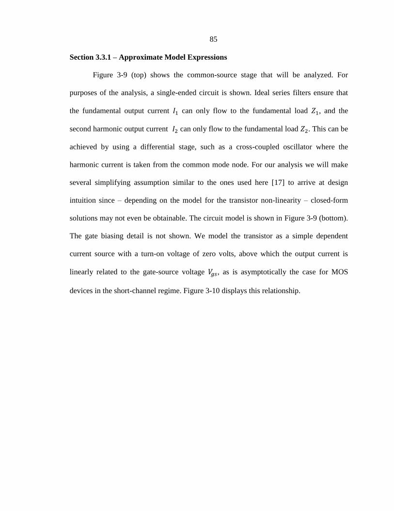
85
Section 3.3.1 – Approximate Model Expressions
Figure 3-9 (top) shows the common-source stage that will be analyzed. For
purposes of the analysis, a single-ended circuit is shown. Ideal series filters ensure that
the fundamental output current can only flow to the fundamental load , and the
second harmonic output current can only flow to the fundamental load . This can be
achieved by using a differential stage, such as a cross-coupled oscillator where the
harmonic current is taken from the common mode node. For our analysis we will make
several simplifying assumption similar to the ones used here [17] to arrive at design
intuition since – depending on the model for the transistor non-linearity – closed-form
solutions may not even be obtainable. The circuit model is shown in Figure 3-9 (bottom).
The gate biasing detail is not shown. We model the transistor as a simple dependent
current source with a turn-on voltage of zero volts, above which the output current is
linearly related to the gate-source voltage , as is asymptotically the case for MOS
devices in the short-channel regime. Figure 3-10 displays this relationship.

86
Figure 3-9: Common source FET circuit
(top) and model (bottom).
Figure 3-10: Output current non-linearity
used for FET circuit of Figure 3-9.
Figure 3-11: Harmonic components of
output current
Figure 3-12: Device voltage and current
in
2in
Vs
Z1
Z2
I2
I1
in
2in
Z1
Z2
I2
I1
Iin
Cgd
Cgs
Vgs
Gm
+
Gate-Source Voltage [V]
Output Current [A]
Slope=Gm
-0.1
0
0.1
0.2
0.3
0.4
0.5
0 0.5 1
Cu
rre
nt M
agn
itu
de
[A]
Fraction "a" FET off-time/on-time
Output Current Harmonic Magnitudes
I1
I2
I3
I4
Time t [A.U.]
Dev
ice
Vo
ltag
e, C
urr
ent
[A.U
.]
Voltage
Current
Vs

87
We assume a sinusoidal input current at the fundamental and a transistor bias
such that the transistor is off for a fraction of the time. We assume no input current is
conducted through . The input power is then simply given by
(3-7)
The output current is given by when the transistor is on, and zero
otherwise. To calculate the on-time of the transistor, we would need to take into account
the second-harmonic current feedback through , but this is a small contribution, so we
ignore this contribution to for now (we will come back to this point later). We
calculate the fundamental component of the output current to obtain
( ) [ ( ) ( )] (3-8)
where is the fraction of time the transistor is off. Similarly, the second-harmonic
output current component is
( ) ( ) (3-9)
and the third-harmonic current and fourth-harmonic currents can be expressed as
( )
[ ( )] (3-10)
The magnitudes for values of between zero and one for the first four harmonic currents
are plotted in Figure 3-11, with ( ) ⁄⁄ , such that the fundamental
component evaluates to one for . The second-harmonic output current is maximized
for ⁄ and we can ignore higher-order components at that point. Because we have

88
not modeled any gain-compression for high gate-source voltages, the generated harmonic
current ratios are independent of the gate-source voltage swing as long as the duty cycle
of the transistor is the same. Starting from a bias point with and increasing , the
first component in the series expansion for is proportional to ⁄ , and hence the first
series component in is proportional to , as expected.
To calculate output power, we need to determine the appropriate load resistance.
From a small-signal model, the resistive part of the output impedance in the small signal
regime is approximately given by [17]:
. (3-11)
An expression for the output impedance of the stage in large signal operation can be
derived by taking into account the capacitive current through and and adding the
fact that current through the dependent current source flows only for a fraction ( )
through the current source. We obtain
( )
(3-12)
where ( ) ⁄ ( ) is the fundamental output current reduction factor and
( )⁄ is the unity gain frequency. We can express the fundamental
power delivered to the load to the input power as (also comp. [17])
(3-13)
Setting this expression to one, we calculate
89
√
(3-14)
The equation simplifies to Lee’s expression for (Class-A regime). The maximum
power gain frequency for the fundamental thus drops as the inverse of the square root of
the duty cycle (such that in Class B operation the unity power gain frequency is
approximately 70% of the unity gain frequency in Class A). The approach made is thus
equivalent to reducing the fundamental output current by the duty cycle and increasing
the output resistance accordingly for the same output voltage. It is also equivalent to
reducing the effective by a factor of .
We continue by calculating the maximum second-harmonic output power. The
optimum output resistance is given by the above formula and does not change over
frequency significantly. The second harmonic output power is then found to be
( ) (
( )
( ( ) ( )) )
(3-15)
The term in parentheses is the ratio of the reduced fundamental output current to the full
( ) second harmonic current times a feedback factor , and reduced by a factor of
two since only half the harmonic current will end up in the load. The feedback factor
occurs because the second-harmonic current fed-back to the gate itself produces a gate-
source voltage. Using a linear approximation, we can express the additional current due
to this feedback as (such that the total output current is
( )), and
solving
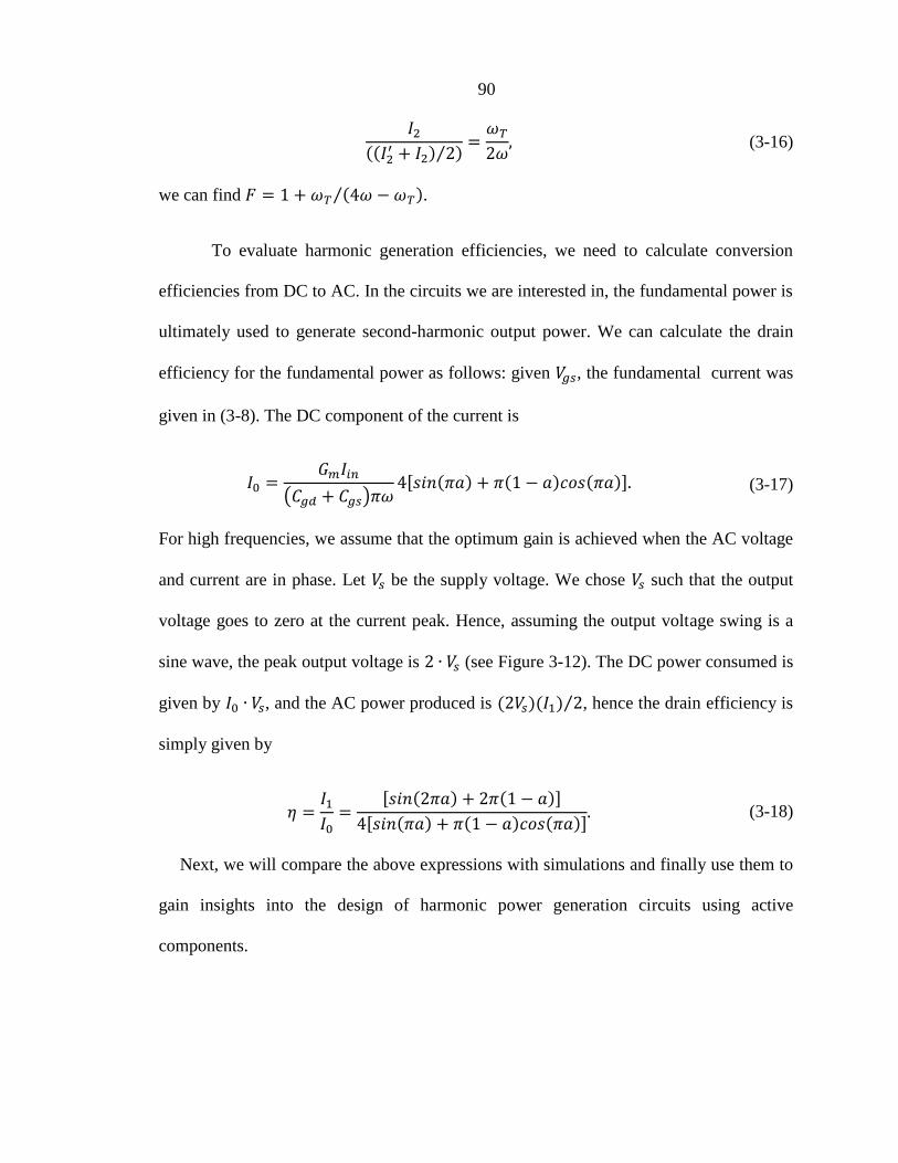
90
(( ) ⁄ )
(3-16)
we can find ( )⁄ .
To evaluate harmonic generation efficiencies, we need to calculate conversion
efficiencies from DC to AC. In the circuits we are interested in, the fundamental power is
ultimately used to generate second-harmonic output power. We can calculate the drain
efficiency for the fundamental power as follows: given , the fundamental current was
given in (3-8). The DC component of the current is
( ) [ ( ) ( ) ( )] (3-17)
For high frequencies, we assume that the optimum gain is achieved when the AC voltage
and current are in phase. Let be the supply voltage. We chose such that the output
voltage goes to zero at the current peak. Hence, assuming the output voltage swing is a
sine wave, the peak output voltage is (see Figure 3-12). The DC power consumed is
given by , and the AC power produced is ( )( ) ⁄ , hence the drain efficiency is
simply given by
[ ( ) ( )]
[ ( ) ( ) ( )] (3-18)
Next, we will compare the above expressions with simulations and finally use them to
gain insights into the design of harmonic power generation circuits using active
components.

91
Section 3.3.2 – Model Comparison with Simulation
Since the expressions developed above use several approximations, we compare
their accuracy with results obtained from simulations. For the model simulations, the
following values are used: , , , and . With
these values, we predict a unity power-gain frequency of . We simulate gain
over frequency and compare with predictions from (3-13), shown in Figure 3-13. As is
evident, the calculation versus the simulation agrees well, particularly at high
frequencies.
As noted previously, the unity power gain frequency decreases as the device duty
cycle is lowered. From (3-13), we predict that the unity gain frequency drops by a factor
proportional to the square root of the duty cycle. We compare simulated unity gain
frequencies versus the calculated values, as shown in Figure 3-14, versus the current
reduction factor . The agreement is acceptable. The remaining error is mostly due to the
difference in simulated on-time versus calculated on-time.
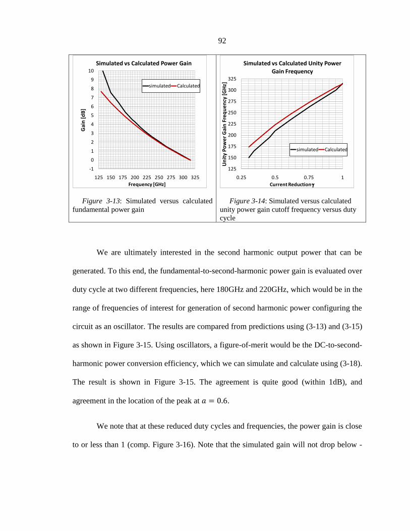
92
Figure 3-13: Simulated versus calculated
fundamental power gain
Figure 3-14: Simulated versus calculated
unity power gain cutoff frequency versus duty
cycle
We are ultimately interested in the second harmonic output power that can be
generated. To this end, the fundamental-to-second-harmonic power gain is evaluated over
duty cycle at two different frequencies, here 180GHz and 220GHz, which would be in the
range of frequencies of interest for generation of second harmonic power configuring the
circuit as an oscillator. The results are compared from predictions using (3-13) and (3-15)
as shown in Figure 3-15. Using oscillators, a figure-of-merit would be the DC-to-second-
harmonic power conversion efficiency, which we can simulate and calculate using (3-18).
The result is shown in Figure 3-15. The agreement is quite good (within 1dB), and
agreement in the location of the peak at .
We note that at these reduced duty cycles and frequencies, the power gain is close
to or less than 1 (comp. Figure 3-16). Note that the simulated gain will not drop below -
-1
0
1
2
3
4
5
6
7
8
9
10
125 150 175 200 225 250 275 300 325
Gai
n [
dB
]
Frequency [GHz]
Simulated vs Calculated Power Gain
simulated Calculated
125
150
175
200
225
250
275
300
325
0.25 0.5 0.75 1
Un
ity
Po
we
r G
ain
Fre
qu
en
cy [
GH
z]
Current Reduction g
Simulated vs Calculated Unity Power
Gain Frequency
simulated Calculated
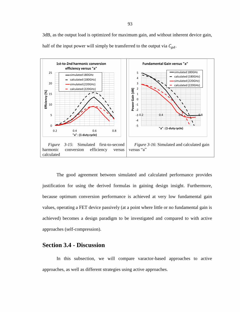
93
3dB, as the output load is optimized for maximum gain, and without inherent device gain,
half of the input power will simply be transferred to the output via .
Figure 3-15: Simulated first-to-second
harmonic conversion efficiency versus
calculated
Figure 3-16: Simulated and calculated gain
versus “a”
The good agreement between simulated and calculated performance provides
justification for using the derived formulas in gaining design insight. Furthermore,
because optimum conversion performance is achieved at very low fundamental gain
values, operating a FET device passively (at a point where little or no fundamental gain is
achieved) becomes a design paradigm to be investigated and compared to with active
approaches (self-compression).
Section 3.4 - Discussion
In this subsection, we will compare varactor-based approaches to active
approaches, as well as different strategies using active approaches.
0
5
10
15
20
25
0.2 0.4 0.6 0.8
Effi
cie
ncy
[%
]
"a" : (1-duty cycle)
1st-to-2nd harmonic conversion
efficiency versus "a"
simulated 180GHz
calculated (180GHz)
simulated (220GHz)
calculated (220GHz)
-5
-4
-3
-2
-1
0
1
2
3
4
5
0.2 0.4 0.6 0.8
Po
we
r G
ain
[d
B]
"a" : (1-duty cycle)
Fundamental Gain versus "a"
simulated 180GHz
calculated (180GHz)
simulated (220GHz)
calculated (220GHz)

94
To first compare varactor-based approaches with active approaches, we
investigate the scaling of the various figures of merit with device size. In a short-channel
approximation, will scale with the inverse of the gate length, as [17]
(3-19)
The product of the gate resistance and the gate-drain capacitance will similarly scale
proportionally to the gate length. While we expect, the gate resistance for a given device
width to scale inversely to gate length, shorter minimum device widths are typically
available in more advanced technology nodes, leaving the overall gate resistance
constant. Similarly, the gate-drain overlap capacitance should scale inversely to the gate
length, offset by thinner gate oxides. However, oxide thicknesses are no longer
decreasing linearly with the technology node. These assumptions, while somewhat
oversimplifying the picture, still predict a scaling of inversely proportional to gate
length, in accordance with observed data [44] as well as the ITRS technology roadmap
[51].
For the MOS varactor capacitances, and , we can reasonably assume
that they scale the same with the gate length. Hence, the varactor cutoff frequency will
scale inversely to the product of device capacitance and gate/channel resistance. This
product, for the same reasons as above, will scale approximately linearly with the device
length; hence we deduce that the cutoff frequency of MOS varactors will be inversely
proportional to the minimum available gate length in the technology. Thus, as CMOS
processing technology advances to smaller minimum gate lengths, we expect no relative
advantage of one approach over the other.

95
We can also gain insight into absolute differences between MOS varactor and
active approaches by comparing cutoff frequencies achievable for MOS varactors versus
at a particular technology node.
We can bound the cutoff frequency by writing
( )
(3-20)
where ⁄ and . We express the product of as a ratio of
to to obtain
( )
(3-21)
From this, we expect to be somewhat greater than . Typically, the ratio of on-to-
off capacitance is close to or less than 2 (three-half typically), hence we expect the ratio
of to to be comparable to the ratio of to . Thus, for any given technology
node, the core conversion efficiency of MOS varactors is expected to be higher than of
any active circuit. This advantage, however, is typically more than offset by the higher
required quality factor in the matching circuits. To illustrate this point, we note that –
assuming that is constant but small – that efficiency is increased by increasing
beyond all bounds. In this limit, the quality factor has a lower bound set by the product of
and , to wit
(3-22)
Yet, for very large , the efficiency of the doubler is given by

96
( )
(3-23)
Hence, the efficiency can only be increased by increasing the inherent quality factor of
the varactor. Since the varactor needs to be matched at input and output, often several dB
of additional losses are incurred compared to using an active circuit in the matching
passives.
Using an active circuit, two different strategies can be pursued. The first strategy
employs an oscillator. In order to derive the obtainable efficiency, we employ the same
compression model as previously. We note that below , we feed back the
fundamental output power to the input. Thus, the oscillator duty cycle – and hence the
generated second harmonic power – is determined by the duty cycle at which the
fundamental power gain is reduced to one. Since the variables are related in a non-
algebraic way, the solution cannot be expressed in closed form, but can be easily
determined numerically. Namely, we set the fundamental power gain to 1 to obtain
(
)
(3-24)
from which we calculate (the numerical step), and from we obtain the drain
efficiency, and, hence, the overall DC-to-second harmonic efficiency. This efficiency is
only a function of the fundamental frequency, and is plotted in (on a logarithmic scale).
We note that the theoretical efficiency increases as the oscillation frequency is decreased,
as the DC-to-fundamental and fundamental-to-second harmonic conversion efficiencies
both increase at reduced duty cycles.

97
We compare the simple oscillator topology with a topology of a driven oscillator:
an oscillator driven with additional power of a second, fundamental oscillator. In this
second scenario, it may become possible to drive to second oscillator deeper into
compression using the power of the fundamental oscillator; hence additional degrees of
freedom are obtained to maximize the DC-to-second harmonic conversion efficiency.
With two oscillators (one driving and one generating), two variables exist: (1) the chosen
duty cycle of the second oscillator (chosen such that the gain is less than one), and (2) the
chosen duty cycle of the fundamental oscillator (gain greater than 1). The size ratio of the
two oscillators can then be determined to be able to use any surplus power of the first
oscillator to drive the second oscillator. For each operating frequency, we can find the
optimum choice of the above two parameters, and compare the overall conversion
efficiency to the conversion efficiency obtained from a single oscillator. The results are
also plotted in Figure 3-17. For the second possibility (fundamental oscillator followed
by a doubler), we again plot the conversion efficiencies, this time versus the duty cycle of
the second oscillator (doubler). We only allow duty cycles that produce a gain of less
than one, hence requiring the fundamental oscillator to provide additional conversion
power. The results are shown in Figure 3-18. The horizontal lines mark the values
obtained for a single oscillator (compare Figure 3-17).

98
Figure 3-17: Conversion loss (DC-to-
second harmonic) for single oscillator (red) and
optimized oscillator-doubler combination
(black), assuming no DC conduction in doubler
Figure 3-18: Conversion loss (DC-to-
second harmonic) for oscillator-doubler
combination at =0.6max (black) and
=0.8max (red) versus doubler duty cycle.
Lines are values for simple oscillator.
As is evident, a single oscillator always has greater conversion efficiency from
DC to second harmonic power than any simple combination. This is intuitively clear,
since the single oscillator subsumes the doubler, but may be run at higher drain
efficiencies.
However, by observing the waveforms produced by the doubler carefully, we note
that the doubler itself does not require DC power for high compression operation since
the device provides very little gain, and no current flows for most of the period, thus
negative voltages can be sustained while the device is off. We can recalculate the
conversion efficiency, this time only accounting for the efficiency of the fundamental
oscillator (without utilizing its harmonic output). Redoing the calculation, choosing
values that maximize the conversion efficiency for both oscillator duty cycles, we obtain
-25
-20
-15
-10
-5
0.5 0.6 0.7 0.8 0.9
Co
nve
rsio
n L
oss
[d
B]
Frequency/fmax
DC-to-Second Harmonic Calculated
Conversion Efficiency
Simple OscillatorOptimized, no DC
-25
-20
-15
-10
-5
0.5 0.6 0.7 0.8 0.9
Co
nve
rsio
n L
oss
[d
B]
Duty Cycle of Doubler
DC-to-Second Harmonic Calculated
Conversion Efficiency
w/wmax=0.6w/wmax=0.8
99
the curve in Figure 3-17 (red curve). By comparison, for high operating frequencies, the
conversion efficiency compared to the a simple oscillator is increased because the
doubler can be driven deeper into compression without requiring unity power gain at the
fundamental and using DC current. The optimal ratio as the frequency is increased is
towards a larger fundamental oscillator and a successively smaller doubler.
Using this approach (not requiring the doubler to carry DC current) has another
practical advantage: the maximum current densities for integrated devices are much
larger for AC currents than for DC currents. Allowing only AC currents in the doubler
allows the use of smaller metal lines in the layout, reducing parasitic device capacitances.
Since at millimeter wave frequencies, capacitances as small as one femtofarad can
significantly impact the overall conversion efficiency, such that reducing layout parasitics
becomes important.
It must be mentioned, though, that separating the functions of providing
fundamental power and performing the frequency conversion into separate devices
inherently complicates the design, as additional matching passives are needed,
introducing further losses and resulting in a less simple (and potentially less reliable)
design. Having quantified and discussed these choices, however, gives us necessary
insight for the designs to follow.
Section 3.5 – Summary and Conclusion
In this chapter, we have discussed strategies for generating millimeter wave
power using CMOS integrated circuit technology. The design of varactor frequency
converters as well as active frequency converters was discussed, using models developed

100
that were compared with simulations as well as additional measurements. The insights
gained are used subsequently in the design of the frequency conversion core cells in the
systems to be discussed in the following two chapters.
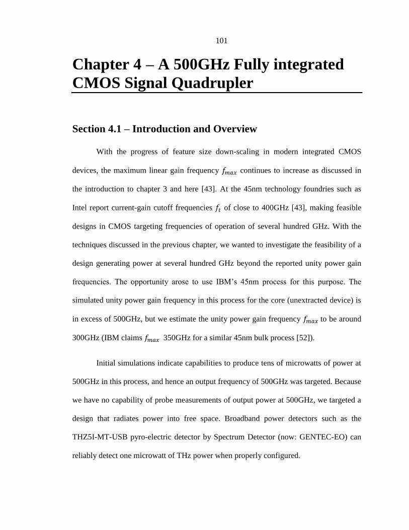
101
Chapter 4 – A 500GHz Fully integrated
CMOS Signal Quadrupler
Section 4.1 – Introduction and Overview
With the progress of feature size down-scaling in modern integrated CMOS
devices, the maximum linear gain frequency continues to increase as discussed in
the introduction to chapter 3 and here [43]. At the 45nm technology foundries such as
Intel report current-gain cutoff frequencies of close to 400GHz [43], making feasible
designs in CMOS targeting frequencies of operation of several hundred GHz. With the
techniques discussed in the previous chapter, we wanted to investigate the feasibility of a
design generating power at several hundred GHz beyond the reported unity power gain
frequencies. The opportunity arose to use IBM’s 45nm process for this purpose. The
simulated unity power gain frequency in this process for the core (unextracted device) is
in excess of 500GHz, but we estimate the unity power gain frequency to be around
300GHz (IBM claims 350GHz for a similar 45nm bulk process [52]).
Initial simulations indicate capabilities to produce tens of microwatts of power at
500GHz in this process, and hence an output frequency of 500GHz was targeted. Because
we have no capability of probe measurements of output power at 500GHz, we targeted a
design that radiates power into free space. Broadband power detectors such as the
THZ5I-MT-USB pyro-electric detector by Spectrum Detector (now: GENTEC-EO) can
reliably detect one microwatt of THz power when properly configured.

102
In order to generate power at 500GHz, well beyond the estimated and reported
, and to investigate the feasibility of the active up-conversion designs discussed in
the previous chapters, we decided for a frequency quadrupler based design similar to the
doubler designs discussed previously. From the discussion of Section 3.3.1 –
Approximate Model Expressions, we can readily extend the design insights gained
previously to a fourth-harmonic up-conversion circuit. In particular, we would expect
conversion efficiencies of 16% compared to the ones obtainable for a frequency doubler,
thus within our targeted range of tens of microwatts of output power.
Because fully integrated antennas in a CMOS process can suffer from a variety of
design issues such as low radiation efficiency due to excitation of substrate modes and
resistive losses in the substrate, we decided to use patch antennas. While integrated patch
antennas even at 500GHz exhibit narrow bandwidths, they avoid many of the other issues
of fully integrated antennas.
This design serves as a test vehicle to explore the feasibility of design targeting
the sub-millimeter wave frequency range using a commercial CMOS process as the
implementation vehicle.
Section 4.2 – System and Block Level Design
In this section we will in detail describe the design both on the system as well as
the block level. A subsection is reserved for each of the various aspects of the design.

103
Section 4.2.1 – Antenna Design
Because of the difficulties associated with designing fully integrated antennas, we
chose to use patch antennas because the frequency of operation is high enough to provide
reasonable bandwidth. The bandwidth of a patch antenna can be estimated by [53]
[( )
] (4-1)
To design the antenna, we follow the procedure outlined in [54]. The substrate thickness
of the silicon dioxide is m, the relative permittivity is and the design
frequency . A starting point for a width can be found using [54]
√
√
⁄
(4-2)
and for the length, using [54], we find (comp. p. 819)
[
]
(4-3)
We use these values as the starting point for a design, and use an electromagnetic solver
(IE3D) optimizing the width and length. The antenna will be placed on top of a finite
ground plane that extends 30m to 80m on all sides (depending on the side), compare
Figure 4-1. The solver will optimize radiation efficiency. The final values are
, that is, the optimization greatly extends the width to help radiation
efficiency. Because an increase in width increases the bandwidth, and furthermore
decreases the radiation resistance [53]

104
[
] ( ⁄ ) (4-4)
(and hence increases the output power), we keep this increased width. The simulated
radiation efficiency and antenna gain is shown in Figure 4-2. The input impedance at
500GHz is approximately 100+30j, and for frequencies +/-15GHz the input reactance
does not change significantly, while the resistive part decreases by a factor of
approximately three.
Figure 4-1: Patch antenna layout
Figure 4-2: Simulated radiation
efficiency and antenna gain
Thus, even using a wide patch antenna, the bandwidth is relatively narrow, approximately
4%-6%. This is a severe disadvantage of integrated patch antennas, even at these high
frequencies. The radiation efficiency in percent is shown in Figure 4-3, and the input
resistance and reactance are shown in Figure 4-4.
Input
connector
Shield (tub) – clearance
~50um
480um
240um
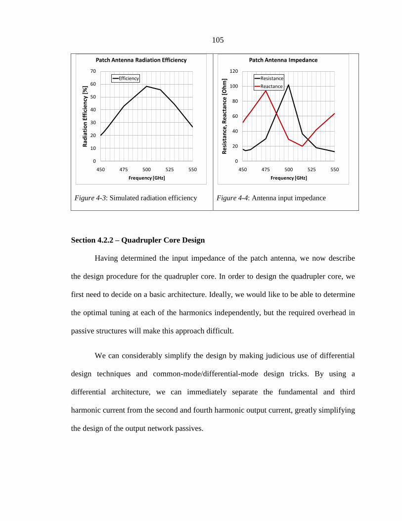
105
Figure 4-3: Simulated radiation efficiency
Figure 4-4: Antenna input impedance
Section 4.2.2 – Quadrupler Core Design
Having determined the input impedance of the patch antenna, we now describe
the design procedure for the quadrupler core. In order to design the quadrupler core, we
first need to decide on a basic architecture. Ideally, we would like to be able to determine
the optimal tuning at each of the harmonics independently, but the required overhead in
passive structures will make this approach difficult.
We can considerably simplify the design by making judicious use of differential
design techniques and common-mode/differential-mode design tricks. By using a
differential architecture, we can immediately separate the fundamental and third
harmonic current from the second and fourth harmonic output current, greatly simplifying
the design of the output network passives.
0
10
20
30
40
50
60
70
450 475 500 525 550
Rad
iati
on
Eff
icie
ncy
[%
]
Frequency [GHz]
Patch Antenna Radiation Efficiency
Efficiency
0
20
40
60
80
100
120
450 475 500 525 550
Re
sist
ance
, Re
acta
nce
[O
hm
]
Frequency [GHz]
Patch Antenna Impedance
Resistance
Reactance
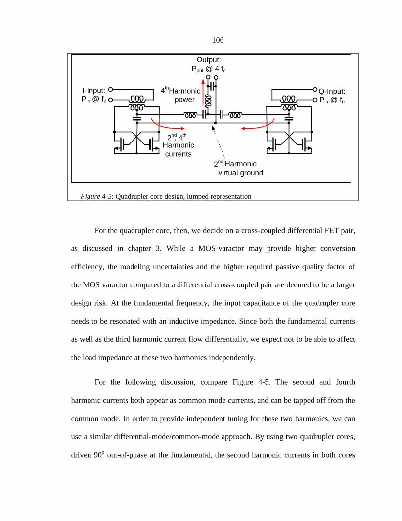
106
Figure 4-5: Quadrupler core design, lumped representation
For the quadrupler core, then, we decide on a cross-coupled differential FET pair,
as discussed in chapter 3. While a MOS-varactor may provide higher conversion
efficiency, the modeling uncertainties and the higher required passive quality factor of
the MOS varactor compared to a differential cross-coupled pair are deemed to be a larger
design risk. At the fundamental frequency, the input capacitance of the quadrupler core
needs to be resonated with an inductive impedance. Since both the fundamental currents
as well as the third harmonic current flow differentially, we expect not to be able to affect
the load impedance at these two harmonics independently.
For the following discussion, compare Figure 4-5. The second and fourth
harmonic currents both appear as common mode currents, and can be tapped off from the
common mode. In order to provide independent tuning for these two harmonics, we can
use a similar differential-mode/common-mode approach. By using two quadrupler cores,
driven 90o out-of-phase at the fundamental, the second harmonic currents in both cores
I-Input:
Pin @ fo
Q-Input:
Pin @ fo
Output:
Pout @ 4 fo
2nd, 4
th
Harmonic
currents
4th Harmonic
power
2nd Harmonic
virtual ground

107
will be out-of-phase while the fourth harmonic current in both cores will be in phase.
Connecting the common mode nodes of both cores, we can create a virtual ground at the
center point for the second harmonic while creating a common mode point there for the
fourth harmonic. Thus, the second harmonic will see whatever connection impedance
exists from the quadrupler devices to this common mode point, while the fourth harmonic
will see the same impedance plus whatever additional impedance we choose to connect
from this common mode point to the antenna input. Using this type of architecture, we
expect to be able to provide independently controllable loads for the fundamental, second
and fourth harmonic, again compare Figure 4-5.
In order to design the quadrupler core, we convert the conceptual design step-by-
step to a layout. We begin with all ideal passives, loading the fundamental and third
harmonic equally. We begin by choosing a load resistance. In order to maximize the
power produced, we would like to use a load resistance that is as small as possible.
However, since we are constrained by the antenna impedance at 500GHz, we choose a
value of 33, which is 1/3 of the antenna input resistance. This choice is made with the
following considerations: at 500GHz, we expect to be able to fabricate passives with a
quality factor of less than ten. In order to keep passive losses reasonable, we note that the
efficiency of a simple impedance transformation network is given by
(4-5)
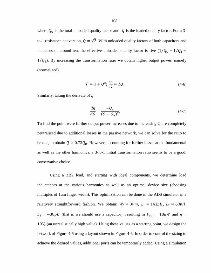
108
where is the total unloaded quality factor and is the loaded quality factor. For a 3-
to-1 resistance conversion, √ . With unloaded quality factors of both capacitors and
inductors of around ten, the effective unloaded quality factor is five ( ⁄ ⁄
⁄ ). By increasing the transformation ratio we obtain higher output power, namely
(normalized)
(4-6)
Similarly, taking the derivate of
( ) (4-7)
To find the point were further output power increases due to increasing Q are completely
neutralized due to additional losses in the passive network, we can solve for the ratio to
be one, to obtain . However, accounting for further losses at the fundamental
as well as the other harmonics, a 3-to-1 initial transformation ratio seems to be a good,
conservative choice.
Using a 33 load, and starting with ideal components, we determine load
inductances at the various harmonics as well as an optimal device size (choosing
multiples of 1um finger width). This optimization can be done in the ADS simulator in a
relatively straightforward fashion. We obtain: , , ,
(that is we should use a capacitor), resulting in and
(an unrealistically high value). Using these values as a starting point, we design the
network of Figure 4-5 using a layout shown in Figure 4-6. In order to control the sizing to
achieve the desired values, additional ports can be temporarily added. Using a simulation

109
test-bench with the then current layout, and varying series test impedances to see whether
a certain dimension should be increased or decreased, the design procedure follows a
controllable path leading using as few E/M simulation iterations as possible, to arrive at
the final geometry. With the final geometry and all devices in place, the overall
conversion efficiency is simulated to be at .
Figure 4-6: Layout simulation view of quadrupler core network
Included in the design are the input stage transistors (differential pair) used to
amplify the fundamental signal for the quadrupler core. These transistors are located at
the core I-input and core Q-input, respectively.
Section 4.2.3 – Core Amplifier Design
The quadrupler core will be driven with a fundamental input signal at quadrature.
In order to generate the required output power, we require 625W of input power at the
fundamental frequency of 125GHz, not an insignificant amount of power. We design
three amplification stages (not including the quadrupler core amplifier devices) since we
Antenna connector
Core I-inputCore Q-input
Dimensions:
170um by
60um
Quadrupler

110
estimate that the reference signal power routed across the chip will be in the tens of
microwatt that will be used to lock the phase-rotating VCOs to be described in a
subsequent subsection.
Each amplifier stage consists of a single common-source differential pair with
additional feedback and optionally input resistors for stabilization. An inductor is used at
the output to tune out capacitance. Each stage includes additional series transmission line
pieces to connect to the following stage. A schematic of a single stage is shown in Figure
4-7.
The devices use fingers of 0.75m width each to maximize the cutoff frequency.
The core transistors (discussed in the previous section) are sized to produce an output
power in excess of 1mW each to allow for additional losses. With thirty-eight fingers
each, additional input and feedback resistance of 2keach is used for stability. The
power stage is driven by the driver stage, using eighteen fingers/FET, feedback resistance
of 2k and input resistance of 3k, providing a gain of 3.5 at a PAE of 9%. The input
and feedback resistance for this and all amplification stages are chosen to obtain a
minimum stability factor of 1.03. The buffer amplifier requires an input power of 80W
to produce 280W with a PAE of 5.4% (ten fingers/device used). This buffer itself is
driven by the VCO buffer, using five fingers.
At the end of the two chains is the locked I/Q VCO used for local phase-shifting.
The I/Q half-VCOs are independently locked to the incoming I- and Q-reference signals
and can be tuned independently.
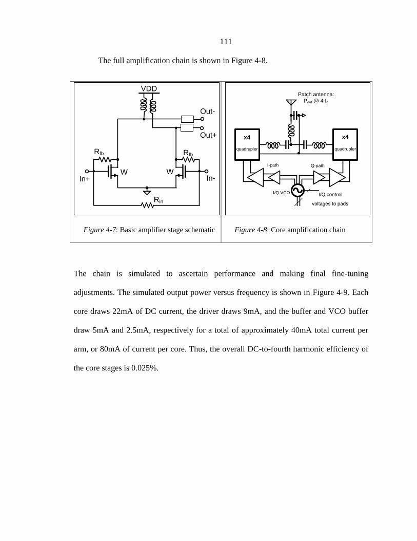
111
The full amplification chain is shown in Figure 4-8.
Figure 4-7: Basic amplifier stage schematic
Figure 4-8: Core amplification chain
The chain is simulated to ascertain performance and making final fine-tuning
adjustments. The simulated output power versus frequency is shown in Figure 4-9. Each
core draws 22mA of DC current, the driver draws 9mA, and the buffer and VCO buffer
draw 5mA and 2.5mA, respectively for a total of approximately 40mA total current per
arm, or 80mA of current per core. Thus, the overall DC-to-fourth harmonic efficiency of
the core stages is 0.025%.
Rfb
In+ In-
Out-
Out+
VDD
Rfb
Rin
W W
x4
quadrupler
Patch antenna:
Pout @ 4 fo
x4
quadrupler
I-path Q-path
I/Q VCO I/Q control
voltages to pads
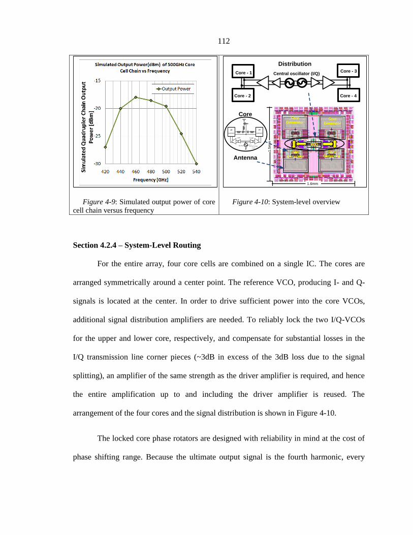
112
Figure 4-9: Simulated output power of core
cell chain versus frequency
Figure 4-10: System-level overview
Section 4.2.4 – System-Level Routing
For the entire array, four core cells are combined on a single IC. The cores are
arranged symmetrically around a center point. The reference VCO, producing I- and Q-
signals is located at the center. In order to drive sufficient power into the core VCOs,
additional signal distribution amplifiers are needed. To reliably lock the two I/Q-VCOs
for the upper and lower core, respectively, and compensate for substantial losses in the
I/Q transmission line corner pieces (~3dB in excess of the 3dB loss due to the signal
splitting), an amplifier of the same strength as the driver amplifier is required, and hence
the entire amplification up to and including the driver amplifier is reused. The
arrangement of the four cores and the signal distribution is shown in Figure 4-10.
The locked core phase rotators are designed with reliability in mind at the cost of
phase shifting range. Because the ultimate output signal is the fourth harmonic, every
Core - 1
Core - 2
Central oscillator (I/Q)
1.5
mm
1.6mm
VCO
Core
Generator
Core
Generator
Core
Generator
Core
Generator
Core - 4
Core - 3
Distribution
Core
Antenna
x4
quadrupler
x4
quadrupler
I-path Q-path
I/Q VCO I/Q control voltages
to pads
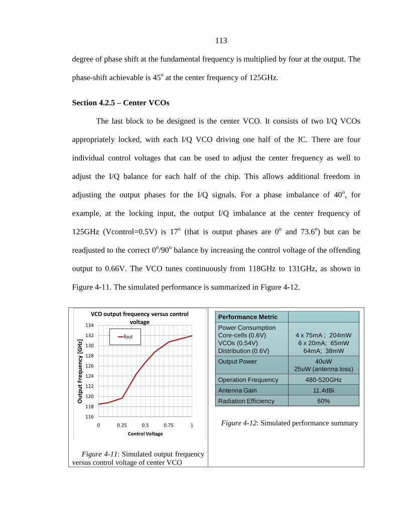
113
degree of phase shift at the fundamental frequency is multiplied by four at the output. The
phase-shift achievable is 45o at the center frequency of 125GHz.
Section 4.2.5 – Center VCOs
The last block to be designed is the center VCO. It consists of two I/Q VCOs
appropriately locked, with each I/Q VCO driving one half of the IC. There are four
individual control voltages that can be used to adjust the center frequency as well to
adjust the I/Q balance for each half of the chip. This allows additional freedom in
adjusting the output phases for the I/Q signals. For a phase imbalance of 40o, for
example, at the locking input, the output I/Q imbalance at the center frequency of
125GHz (Vcontrol=0.5V) is 17o (that is output phases are 0
o and 73.6
o) but can be
readjusted to the correct 0o/90
o balance by increasing the control voltage of the offending
output to 0.66V. The VCO tunes continuously from 118GHz to 131GHz, as shown in
Figure 4-11. The simulated performance is summarized in Figure 4-12.
Figure 4-11: Simulated output frequency
versus control voltage of center VCO
Figure 4-12: Simulated performance summary
116
118
120
122
124
126
128
130
132
134
0 0.25 0.5 0.75 1
Ou
tpu
t Fr
eq
ue
ncy
[G
Hz]
Control Voltage
VCO output frequency versus control
voltage
fout
Performance Metric
Power Consumption
Core-cells (0.6V)
VCOs (0.54V)
Distribution (0.6V)
4 x 75mA ; 204mW
6 x 20mA; 65mW
64mA; 38mW
Output Power 40uW
25uW (antenna loss)
Operation Frequency 480-520GHz
Antenna Gain 11.4dBi
Radiation Efficiency 60%

114
Section 4.3 – Experimental Setup
The IC is taped out in IBMs 45nm silicon-on-insulator process. The chip occupies
an area of 1.5mm by 1.6mm. A die photograph is shown in Figure 4-13. The top-level
aluminum layer (pad-metal) is filled in this process (Figure 4-14), which was unexpected
(since it normally is not filled). The fill pieces are large at a size of 10mx10m, and
may affect the tuning of all passive structures. The chip is wire-bonded in a 44-pin
PLCC, mounted on an FR4 PCB within a socket. The FR4 PCB provides local supply
regulators as well as a control voltage interface connections. The control voltages of the
phase rotators and VCOs are individually connected to pads. They are set manually on a
separate test-board via simple resistive voltage dividers employing trim pots to set the
control voltage in a range of zero to one volt.
Figure 4-13: IBM45nm die photograph
Figure 4-14: Die photograph detail

115
The PCB is shown in Figure 4-15. The DC power drawn by the chip agrees well
with simulation. Because of difficulties using the pyro electric power meter with the lens
setup for the expected power levels, a setup that uses a Pacific Millimeter
downconversion mixer connected to a horn antenna is used. This setup is described in
Chapter 5 in detail. The downconversion mixer, however, is designed for frequencies in
the 220GHz-300GHz band, and we could not procure a 500GHz downconversion mixer,
and horn-antenna combination suitable for operation at 500GHz. The down-converter is
followed by a chain of baseband amplifiers, connected to an Agilent E4448A spectrum
analyzer. The LO signal to the mixer is varied from 20.0GHz to 27.0GHz with the horn
antenna in a variety of different physical locations compared to the circuit to be able to
pick up any radiation if it should exist. After three days of attempting to locate a signal,
using a variety of supply voltage settings and three different bonded chips, no signal
could be located using this setup.

116
Figure 4-15: IBM PCB, mounted on stepper motor setup
Section 4.4 – Summary Remarks
Because of the negative result in detecting any output power, it is difficult to
ascertain the functionality with certainty. The DC power drawn corresponds well to the
power expected in simulation, and because supply connections are plentiful and total
current consumption is relatively modest, no thermal issues are expected (compare
Chapter five). From our experience with the 250GHz chip discussed in the next chapter,
power detection using the power meter is more difficult than anticipated during the tape-
out phase. Even if the circuit produces the full 40W of output power (corresponding to
25W radiated), this power level is difficult to detect using the pyroelectric power meter
since we expect about 3dB loss in the setup itself and thus require almost perfect
alignment since despite the advertised 100nW sensitivity, from experience a few

117
microwatt incident power is required for reliable detection. A downconversion mixer as
used for measurement of the 250GHz setup is more sensitive, but no 500GHz
downconversion mixer is available. Having attempted to detect a signal using the
250GHz setup, we would still expect difficulties, because even if 500GHz could be
detected, we would estimate an additional 30dB of loss in the mixer setup due to antenna
mismatches, use of higher mixing harmonic and general inadequacy. This may be
feasible if the power to be detected is one milliwatt, but assuming that the circuit
produces a full 25uW would correspond to an equivalent 25nW to be detected at
250GHz, an already difficult proposal.
To further investigate the chip, we would require a true 500GHz setup, which we
have so far not been able to procure.
The design procedure itself produced valuable insights, and we do not consider
the effort a failure in that sense. However, further testing using perhaps a borrowed setup
or equipment would be desirable.

118
Chapter 5 – A 250GHz Fully integrated
CMOS Radio Front-End
Section 5.1 – Motivation
As discussed in the introduction and the previous chapter, an increasing research
effort is geared toward combining applications targeted by traditional millimeter wave
and terahertz research (e.g., [55], [56]), most notably imaging [57], spectroscopy and
radar with the power of modern integrated circuit technology to essentially achieve a
quantum step forward in the spread of millimeter wave systems [56] [58], as well as
increase their use to areas traditionally not targeted by millimeter wave systems, such as
communication systems.
The feasibility of integrating an antenna array directly onto a silicon substrate is
investigated in terms of performance trade-offs and driving requirements. In particular,
the effect of the close proximity of the back-side ground-plane is investigated, and
techniques such as outphasing are introduced to control the antenna drive amplitudes and
phase to achieve a globally optimal driving configuration for the antennas in the
packaged array. Furthermore, traditional issues in integrated radio design such as signal
distribution and phase shifting are investigated and implemented to develop a true radio-
frontend for 250GHz, operating beyond the maximum linear gain frequency of this
process. The system is taped out in a commercial 65nm CMOS process and measured to

119
gain valuable experimental insights into the issues of fully integrating radio-frontends
potentially useful for imaging and communications applications.
Section 5.2 – System-Level Design
The design of a fully integrated array system in a silicon substrate begins with
system-level considerations. In this section, we will discuss three aspects of the system-
level design: (1) design of the integrated circuit antennas, (2) amplitude and phase control
of the individual array elements, and, finally (3) issues related to signal-distribution
between the different array elements.
Section 5.2.1 – Antenna Array Design
Because a fully integrated millimeter wave system uses, by definition, antennas
placed on the silicon substrate, the designer is confronted with a variety of well-known
issues of on-chip antenna design that have been studied previously. In particular, because
of the large dielectric constant of silicon, most of the electromagnetic energy will tend to
couple into the silicon substrate rather than into the surrounding air. By reciprocity,
because of the impedance mismatch between air and silicon, incoming electromagnetic
energy is preferentially reflected rather than admitted into the substrate. For these
reasons, the design of the integrated antennas is of great importance, as their sizing and
placement will greatly impact overall system performance as the radiation efficiency of
the array directly impacts overall power efficiency (in transmit mode) as well as

120
sensitivity in receive mode.7 These issues are well known and have been studied
previously, e.g., [59] [60] [61].
For a thin substrate dielectric substrate (less than a couple of wavelengths),
reflections and near-field interactions from the sides and the back of the substrate are
very strong, and will greatly affect the overall antenna performance. In particular, a
grounded, semi-infinite dielectric substrate will support various substrate modes, their
number being determined by the thickness of the substrate. For a dielectric substrate on a
ground-plane, the cutoff frequencies of the supported dielectric modes are given by
(compare, e.g., [62]):
√
( )
√ (5-1)
where , is the speed of light (in vacuum), is the substrate
thickness and is the relative permeability of the substrate material. As noted from the
above, the substrate will always support a TM0 mode and an additional mode for
approximately every quarter-wavelength ( ( ) ⁄ to be exact) of substrate thickness.
Both for a single antenna, as well as an antenna array, these cutoff frequencies
correspond to relative maxima (for the TE mode cutoff frequencies) and minima (for the
TE mode cutoff frequencies) of radiation efficiency (for dipole-type antennas). This
dependency of radiation efficiency on substrate thickness can also be observed for back-
side radiation, and necessitates choosing an optimal substrate thickness depending on the
intended frequency of usage if integrated antennas are to be employed. In the next
7 Because of reciprocity, transmit and receive performance of any antenna are identical. Whenever we
are using the phrase radiation efficiency we imply antenna efficiency.

121
chapter, we will introduce the use of buried antenna elements to circumvent this
restriction.
For very thin substrates (below the TE1 cutoff frequencies) antenna efficiencies
are very high, not only because the substrate only allows a TM0 mode but also because
any losses in the substrate are minimized as the mean path-length through the substrate
for the mode (and hence losses) is minimized. However, a very thin substrate will result
in electromagnetic energy being coupled into and out of the substrate from many
different angles, and very little control over directionality is possible. This is intuitively
clear, since for distances to a back-side ground-plane of less than a quarter-wavelength,
the virtual image of any antenna element is closer than half a wavelength and will
intuitively affect the pattern more strongly than an adjacent element in a phased-array.
Using a substrate thickness corresponding to the next maxima of antenna efficiencies
provides more control over the available antenna patterns, albeit at the expense of
increased dielectric losses, particularly when highly-doped semiconductor substrates are
used.
This dependence is shown in Figure 5-1 for a lossless, semi-infinite silicon
substrate. For a real-world, finite substrate, electromagnetic energy coupled into substrate
modes will eventually leak out. For a substrate with losses, the heights of the peaks in
antenna efficiency tend to decrease as thicker substrates are used (see also [62].
The choice of antenna type (e.g., dipole, loop, etc.) will influence sizing
requirements. However, in terms of losses or antenna efficiencies, numerical simulations
indicate that the dominant determinant of antenna efficiency is the directivity of the

122
antenna (array) used. Thus, while single dipole antennas typically perform worse than
other antenna primitives with higher directivity, this disadvantage largely disappears in
an array. Shown in Figure 5-2 is the antenna loss for a single antenna on a semi-infinite,
lossy silicon substrate using an optimized size for dipole and loop antennas versus die
thickness, taking also metal losses into account.
Figure 5-1: Antenna efficiency (radiation loss)
shown for a dipole antenna of a lossless Si substrate.
Figure 5-2: Antenna loss in dB for
a dipole and a loop antenna on a semi-
infinite, lossy (10cm) Si substrate
For the design presented here, a dipole primitive was chosen.
Next in the design is the sizing of the antenna itself. For a free-space dipole
antenna, a quarter-wavelength is frequently used. However, because the antenna is
situated in a high-permeability substrate, but ultimately radiating to air, the sizing of the
antenna is a variable to be determined. Here, we used Zeland’s IE3D electromagnetic
simulation software to simulate the efficiency as function of dipole length, taking into
account losses of the metal as well as the substrate. For a dipole at a design frequency of
250GHz, the optimal length is mostly independent of substrate height, and – at 500m
-30
-25
-20
-15
-10
-5
0
200 250 300 350 400 450 500 550 600
Ra
dia
tio
n lo
ss [
dB
]
Frequency [GHz]
Simulation radiation efficiencies, dipole on 250um
grounded Si lossless versus frequencies
Z=250u
TE2 TM2 TE3 TM3
-20
-15
-10
-5
0
0 250 500 750 1000
An
ten
na
Loss
[dB
]
Die Thickness
Radiation Efficiency, Single
Loop/Dipole versus Die Thickness
Loop
Dipole

123
for a differential dipole-shaped antenna – corresponds to 43% of the wavelength in free-
space and 150% of the wavelength in silicon.
The antenna efficiency achievable for a single such dipole on a 250m Si
substrate (chosen because it corresponds to the standard shipped die thickness for the
UMC process chosen) is 30% (or 5dB loss), less than the previously simulated loss since
a finite substrate size was chosen.
To increase the radiation efficiency and add functionality, several antennas are
combined in an array. Because the antennas are located in close proximity to each other,
they tend to couple strongly and affect each other’s performance. Because of this affect, a
typical phase-array approach (in-phase drive at the same amplitude for broadside
radiation) – although improving much on the efficiency of a single antenna – does not
yield the optimal performance. In order to determine an optimal driving strategy, the
phases and the amplitudes of the sources are determined using a custom MATLAB
program that maximizes power transfer from the array to a “detector” antenna in the
broadside direction is used. This program is described in detail in Section 6.3.3 .
Shown in Figure 5-3 is the simulated radiation loss of a single antenna versus
substrate height for the particular process used (UMC 65nm). The final design uses a 4 x
2 antenna array (with a 1 x 2 array design as a test-chip). The antennas are spaced half a
wavelength (in air) apart on the dielectric. Simulated radiation efficiency of the entire
array is 58% with an array gain of 10.9dB.

124
Figure 5-3: Radiation loss of single
dipole in UMC65nm process technology
versus substrate thickness
Figure 5-4: Series addition of two frequency
sources in series.
Section 5.2.2 – Element Amplitude and Phase-Control
The millimeter wave radio front-end is designed in UMC’s 65nm CMOS process
that has an FET of around 220GHz. In order to generate and receive signals at
250GHz, a differential frequency doubling stage is used at the output (compare Section
3.3 – Active Approaches in CMOS). This stage operates at a fundamental frequency of
125GHz, producing power at 250GHz due to FET device compression.
In order to control the radiation pattern, it is desirable to control the amplitude and
the phase of the generated 250GHz signal. However, doing so reliably is difficult because
gain at 125GHz comes at a premium (with approximately 5dB available gain at 125GHz).
With so little available gain, any modeling inaccuracy in the FETs will greatly impact the
performance of even the simplest circuit blocks, making it difficult to reliably design
blocks such as gain-and phase-control blocks.
Rload
Sin(t+q1+f1)
Iload
Sin(t+q1-f1)

125
Gain control can be achieved in a variety of ways. For a differential frequency
doubling stage, we expect any gain reduction at the fundamental frequency to result at
approximately twice the reduction at the second harmonic output if we assume that the
second harmonic is produced by gain compression that can be modeled using a
polynomial expression, to wit
(5-2)
A disadvantage of this approach is that it requires the input signal to be reduced, which
may be impossible if an oscillator is used such that any reduction in the input signal
requires a reduction in the output signal and hence may lower the loop-gain of the
oscillator to below one, making it impossible for oscillations to start up.
An alternative that is used in our design is to use an outphasing approach at the
second harmonic. Outphasing is traditionally used in power amplifier design [64] [65].
The advantage of this approach is that the amplitude control at the second harmonic has
little effect on the circuit operation at the fundamental frequency, since the shift in
loading and amplitude happens at the second harmonic. Adding the voltages of two
stages in series (compare Figure 5-4), we can write the output voltage and current as
( ) ( )
(5-3)
Thus, the magnitude of the output voltage is a function of the phase difference . The
magnitude of the impedance seen each of the stages is ( )⁄ and the
angle is . Thus, by simply changing the phase-angle, we can affect the output

126
amplitude. Again, because the outphasing in our design is done at the second harmonic
(the stages are isolated at the fundamental frequency), the mismatch effects only occur at
the second harmonic and do not significantly impact the performance at the fundamental
frequency.
Using the differential phase to change the overall output amplitude, we can use
the common mode phase to change the overall phase of the output signal, as shown
above. Thus, in order to control both the differential mode and common mode input
phases to the two output stages, we need to independently control the phases of each of
the input signals. There are several possible approaches to effect a phase change at RF
frequencies and two of the approaches were investigated in detail for this design. In
general, approaches fall into two broad categories, active and passive approaches.
Passive approaches involve electronically tunable delay elements such as
transmission lines or (switched) lumped filters [66]. Purely passive approaches at RF
frequencies have the advantage that their operation does not depend on active device
gain, which comes at a premium at frequencies that are a sizeable fraction of the active
device maximum gain frequency. However, the signal loss has to be compensated for in
some fashion. They do, however, separate the function of providing phase shifts from the
function of providing signal gain, and are therefore more compatible with a functional
block level approach. The biggest disadvantage of passive approaches is that they
frequently require a large layout area
Active approaches fall into three broad categories: active delay-based approaches
[66] [68], Cartesian phase-rotation approaches [69] and locked oscillator-based
127
approaches [70]. In practice, the difference between a delay-based approach and a locked
oscillator approach is a gradual one. An amplification stage that provides a large amount
of signal delay typically exhibits an under-damped response (i.e., exhibits gain peaking),
and an oscillator is, in some sense, an amplification stage that exhibits infinite gain
peaking. Using an oscillator has the advantage that an oscillator can, in theory, provide
full phase shift. In particular, Adler’s equation [71] can be written as
(
) (5-4)
where is the free-running frequency, is the frequency difference between locking
signal and free-running frequency, is the oscillator quality factor and and are the
oscillator amplitude and the locking signal amplitude. Hence, the locking range is limited
to
(5-5)
If oscillators are used, their locking range thus has to encompass the entire range of
desirable operating frequencies, and hence their inherent quality factor has to be low
enough to allow a shallow enough phase shift gradient to be useful. Because the feasible
tuning range of integrated oscillators at very high frequencies is limited, the inherent
quality factor should be large enough to provide appreciable phase shift across the
frequency band of interest. Furthermore, because oscillators are large signal circuits, they
typically provide gain restoration, which is an advantage since we would like to keep the
amplitudes of the two signals in the outphasing stages to be the same amplitude (as we
have previously assumed).

128
Finally, since the phase-shift at the second harmonic is doubled from the phase-
shift accomplished at the fundamental frequency, a single oscillator phase-shifter can
theoretically provide a full phase shift at the output frequency. For a phase-
shift, however, the oscillator is on the verge of being unlocked, and hence two oscillators
are used in series. This lowers the locking range requirement for each oscillator to ,
and also alleviates input signal strength requirements.
Section 5.2.3 – Signal Distribution Design
Signal distribution across an integrated chip has to be carefully planned at very
high frequencies. At high frequencies, signal losses even for signal transmission across
short distances can be significant, and any differences in signal strength across blocks can
lead to noticeable performance degradation that exhibits itself in larger beam side-lobes.
The same holds true for phase mismatches across elements from theoretically determined
ideal phase differences.
Traditionally, amplitude and phase balance issues are best addressed using
system-level layout approaches that minimize path differences and mismatches such as
binary-tree structures (e.g., [72]). In a binary tree (or n-ary tree), the reference signal
from a central voltage-controlled oscillator is distributed in such a way that the path-
length is equalized to every element. To accomplish this, the signal lines to two (or more)
system blocks converge on a point of symmetry where the signals are combined. This
strategy of routing signals to points of symmetry is continued from these points
recursively until a single master signal line is established that carries the reference signal.
Most frequently, especially at high frequencies, binary trees are used. One disadvantage

129
of such a strategy is that it tends to increase the average routing length since each signal
path has to be at least as long as the path from the reference signal oscillator to the cell
that is situated furthest away. More significantly, for routing to arrays that contain
multiple blocks in both horizontal directions, an already transverse path needs to be
reversed, which requires many lines to be placed adjacently to each other and can lead to
local spatial bottlenecks and signal isolation issues.
For the designed system, a binary-tree signal distribution structure was
considered, but ultimately a daisy-chain signal distribution scheme was chosen. The main
reason for choosing the daisy-chain approach was that it simplified the design of the
amplifiers within the chain, as well as being less expensive on die area for signal
distribution. In particular, with maximally 5dB of simulated gain available at the
fundamental frequency of 125GHz, leaving margin for stability as well as modeling
inaccuracies, it was estimated that 3dB of gain was available at the fundamental
frequency. Thus, at each binary junction, the signal strength going into a new branch
would effectively experience no gain, and an additional amplification stage would be
realistically required for each outgoing branch. Because each amplifier would require
inductive loading to resonate with the device capacitance at the frequency of operation,
each binary partition section would quickly become crowded from a layout point of view
unless ample layout space was provided. The required space would interfere significantly
with the antenna placement and would have required large empty layout space,
significantly increasing the die area. Finally, since the transmission line lengths covering
the distances from binary junction to binary junction, differ in length, it proved difficult
to design a single stage that could be used repeatedly given the tight gain and stability

130
margins. The most reliable design would have been a feedback type amplifier that
provides purely real and equal impedance at input and output, such that a transmission
line of matched impedance would have provided a conjugate match for any section
length. However, a multi-transistor amplification stage operating at more than 50% of
that provides any gain would require a multitude of peaking inductors and was
deemed to not provide enough design margin (aside from the huge impact on layout
area).
As an alternative, a daisy-chain approach was chosen, that routes the signal along
a main path across the chip across distances of similar lengths, and branches off a fraction
of the signal power into the core circuitry for final amplification and conversion. While
this approach addressed many of the concerns deemed to be inherent in the binary-tree
approach, it itself suffers from a multitude of disadvantages. Most notably, each core
consists of two frequency-doubler cells that are driven in-phase to provide maximum
output power. Thus, it would be desirable to provide signals of equal phase and amplitude
to both cells in the absence of different control signals. Furthermore, because the
reference signal is routed across the chips, amplified multiple times along the way, some
form of amplitude control and/or restoration has to be introduced.
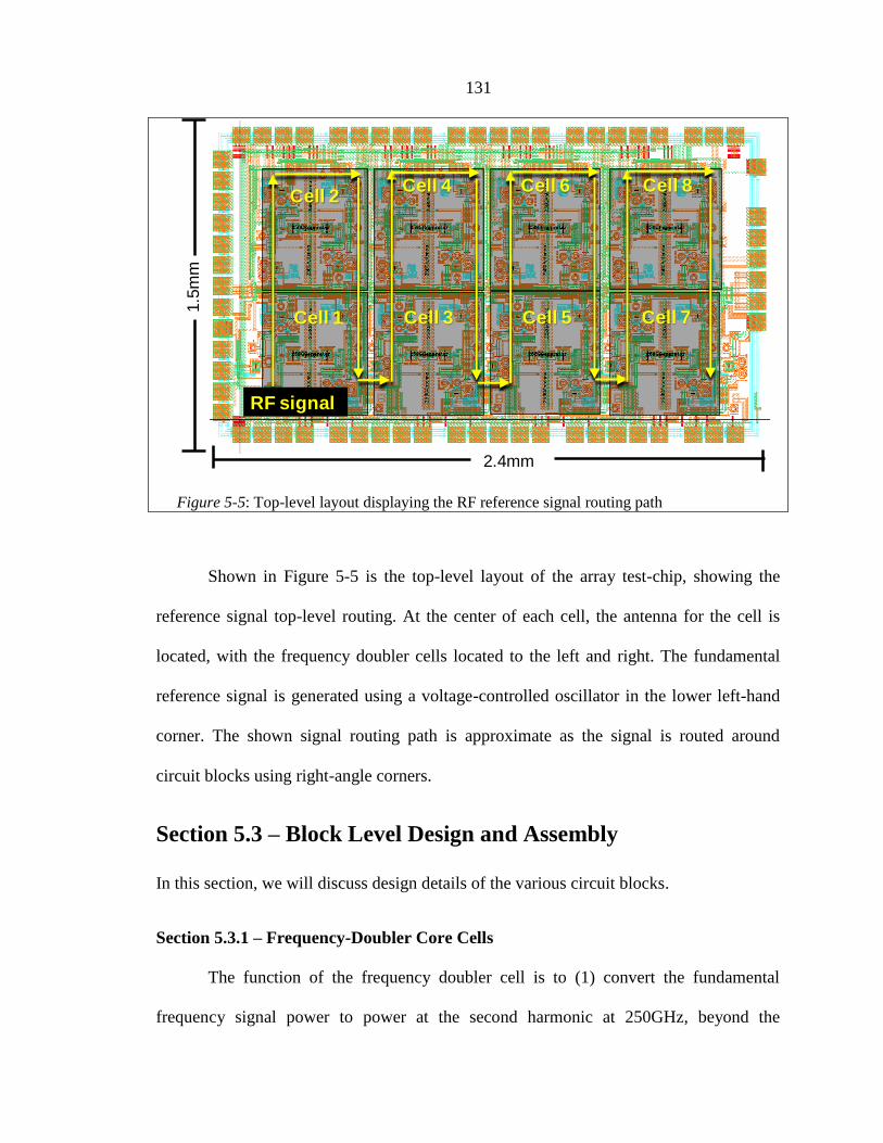
131
Figure 5-5: Top-level layout displaying the RF reference signal routing path
Shown in Figure 5-5 is the top-level layout of the array test-chip, showing the
reference signal top-level routing. At the center of each cell, the antenna for the cell is
located, with the frequency doubler cells located to the left and right. The fundamental
reference signal is generated using a voltage-controlled oscillator in the lower left-hand
corner. The shown signal routing path is approximate as the signal is routed around
circuit blocks using right-angle corners.
Section 5.3 – Block Level Design and Assembly
In this section, we will discuss design details of the various circuit blocks.
Section 5.3.1 – Frequency-Doubler Core Cells
The function of the frequency doubler cell is to (1) convert the fundamental
frequency signal power to power at the second harmonic at 250GHz, beyond the
Cell 1
Cell 2
Cell 3
Cell 4
Cell 5
Cell 6
Cell 7
Cell 8
RF signal
1.5
mm
2.4mm

132
maximum linear gain frequency of the transistor, (2) provide signal combining
functionality for two core cells to allow amplitude and phase control via outphasing by
controlling the phase of the fundamental signal, and (3) provide power combining and
impedance transformation to maximize conversion efficiency and output power.
Figure 5-6: Doubler core cell set. The second harmonic signal current of each doubler cell is
routed from the common mode node through one of the two transformer primaries to generate a
voltage. The voltages are added in the output transformer secondary.
Shown in Figure 5-6 is the schematic for the core doubler cells using a lumped
representation. The output frequency is at the second harmonic of the fundamental
frequency signal that drives the core cell doublers. The output current is driven into an
integrated dipole antenna that connects to a transformer secondary. The transformer has
two independent primary windings coupling to it, such that the voltages over the
primaries are added in series on the secondary. Each primary is wound twice around the
secondary to provide an impedance transformation ratio of 4:1. The integrated circuit
Vdc,2 Vdc,2
2:1
Input B:
Pin @ fo
Output:
Pout @ 2 foSecond harmonic
current
Input A:
Pin @ fo
2:1

133
antennas have rather large input impedances, which help improve their efficiency, but
since the doubler cores are voltage-swing limited, low impedances are necessary to
increase the power output. Since there are two primaries in series, the antenna impedance
is effectively reduced by a factor of eight. The actual transformation is different from the
ideal 8:1 as the coupling coefficient of the transformer windings is less than one,
resulting in a lower ratio. However, an additional series capacitor provides further
impedance transformation, such that the real part of the impedance seen by the doubler
core is 35 for an input impedance of 300.
In order to minimize injection loss of the transformer core, the sizing and spacing
of the primary and secondary windings is successively improved using results from
electromagnetic simulations. In order to minimize the injection loss and keep a large
transformation ratio, the capacitance between primary and secondary windings needs to
be minimized, while keeping the spacing small. Numerous iterations of electromagnetic
simulations indicate that the best approach is to place primary and secondary windings on
different metal layers because the effective spacing in the horizontal direction can be
made small (smaller than the minimum required by DRC rules for metals on the same
layer) – increasing the coupling coefficient – without increasing the capacitance unduly
(since the capacitance – as the metals are pushed underneath each other – is initially
contributed by fringe capacitance rather than parallel plate capacitance).
The transformer is bounded in size in both directions: for very small transformers
the self- and mutual inductance is very small, resulting in a large loaded quality factor
and large circulating reactive currents and hence large losses. For very large transformers,

134
the signal delay at high frequencies becomes noticeable (hence the transformer is no
longer truly a lumped component), and with increasing size, no additional advantages are
gained while resistive losses are increased. Simulation results for different intermediate
sizes are compared for optimal loading and minimal injection loss. The resulting
transformer produces 1.3dB injection loss in simulation and is approximately 30m in
diameter.
The input inductor is similarly designed taking into account similar consideration.
The input transformer is physically larger as it is designed for a center frequency of
125GHz. The turn ratio is 1:1, however, capacitance between the primary and secondary
is used to provide additional impedance transformation. Dozens of designs were
simulated using Zeland’s IE3D electromagnetic simulator, and – using the load presented
by the second harmonic transformers and antenna – the sizing of the primary driving
amplifier and the doubling core are included in a circuit simulation as an optimization
variable. This allows comparing each input transformer design to be compared for both
the output power and overall conversion efficiency achievable. Simulating successive
designs with small incremental changes, in addition to using ideal reactive components in
the optimization to gain insight whether the various components should be increased or
decreased in size, results in a well-tuned design with close to highest conversion
efficiency of the overall structure achievable.
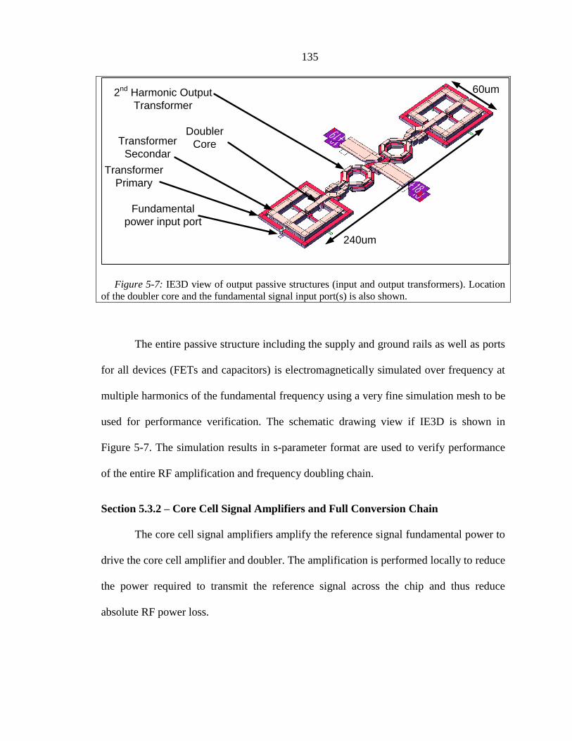
135
Figure 5-7: IE3D view of output passive structures (input and output transformers). Location
of the doubler core and the fundamental signal input port(s) is also shown.
The entire passive structure including the supply and ground rails as well as ports
for all devices (FETs and capacitors) is electromagnetically simulated over frequency at
multiple harmonics of the fundamental frequency using a very fine simulation mesh to be
used for performance verification. The schematic drawing view if IE3D is shown in
Figure 5-7. The simulation results in s-parameter format are used to verify performance
of the entire RF amplification and frequency doubling chain.
Section 5.3.2 – Core Cell Signal Amplifiers and Full Conversion Chain
The core cell signal amplifiers amplify the reference signal fundamental power to
drive the core cell amplifier and doubler. The amplification is performed locally to reduce
the power required to transmit the reference signal across the chip and thus reduce
absolute RF power loss.
Doubler
Core
240um
Fundamental
power input port
Transformer
Primary
Transformer
Secondar
2nd
Harmonic Output
Transformer
60um

136
The amplification chain consists of three stages. The load of the last stage consists
of the doubling core primary transformer discussed above. The previous two stages use
short sections of series differential transmission lines to connect between the output and
the input of the following stage, and provide physical separation from the core passives.
Additional parallel shorted stubs provide impedance transformation as well as a supply
biasing connection.
All amplification stages consist of a single common source differential stage,
shown schematically in Figure 5-8 for the buffer stage. To increase the gain at the desired
frequency, positive feedback via cross-coupled FETs is used. Negative feedback resistors
are used to greatly increase stability at frequencies other than the design frequency while
sacrificing about 1dB of gain at the frequencies of interest. Without these, the common
source stages have a strong tendency to become unstable (particularly with the additional
cross-coupled FETs) at frequencies somewhat below their design frequency, because the
gain is increasing very rapidly with decreasing frequency. Because the real part of the
input impedance at frequencies larger than the design frequency also has a tendency to
become negative, a parallel differential input resistor is used to keep the real part of the
input impedance positive.
The length of the series transmission lines is chosen mostly from layout
considerations. The input impedance looking into the next amplifier stage has a
capacitive reactance, and any length of transmission line will increase this input
capacitance as seen from the previous stage, hence the length of the series line should be
kept to a minimum. By a similar argument, if the shunt line is placed at the input of the
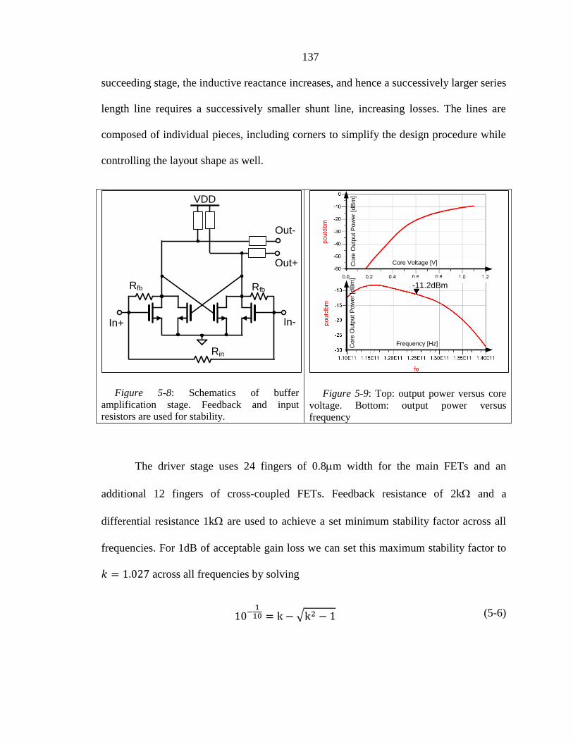
137
succeeding stage, the inductive reactance increases, and hence a successively larger series
length line requires a successively smaller shunt line, increasing losses. The lines are
composed of individual pieces, including corners to simplify the design procedure while
controlling the layout shape as well.
Figure 5-8: Schematics of buffer
amplification stage. Feedback and input
resistors are used for stability.
Figure 5-9: Top: output power versus core
voltage. Bottom: output power versus
frequency
The driver stage uses 24 fingers of 0.8m width for the main FETs and an
additional 12 fingers of cross-coupled FETs. Feedback resistance of 2k and a
differential resistance 1k are used to achieve a set minimum stability factor across all
frequencies. For 1dB of acceptable gain loss we can set this maximum stability factor to
across all frequencies by solving
√ (5-6)
Rfb
In+ In-
Out-
Out+
VDD
Rfb
Rin
Core Voltage [V]Co
re O
utp
ut P
ow
er
[dB
m]
Co
re O
utp
ut P
ow
er
[dB
m]
Frequency [Hz]
-11.2dBm
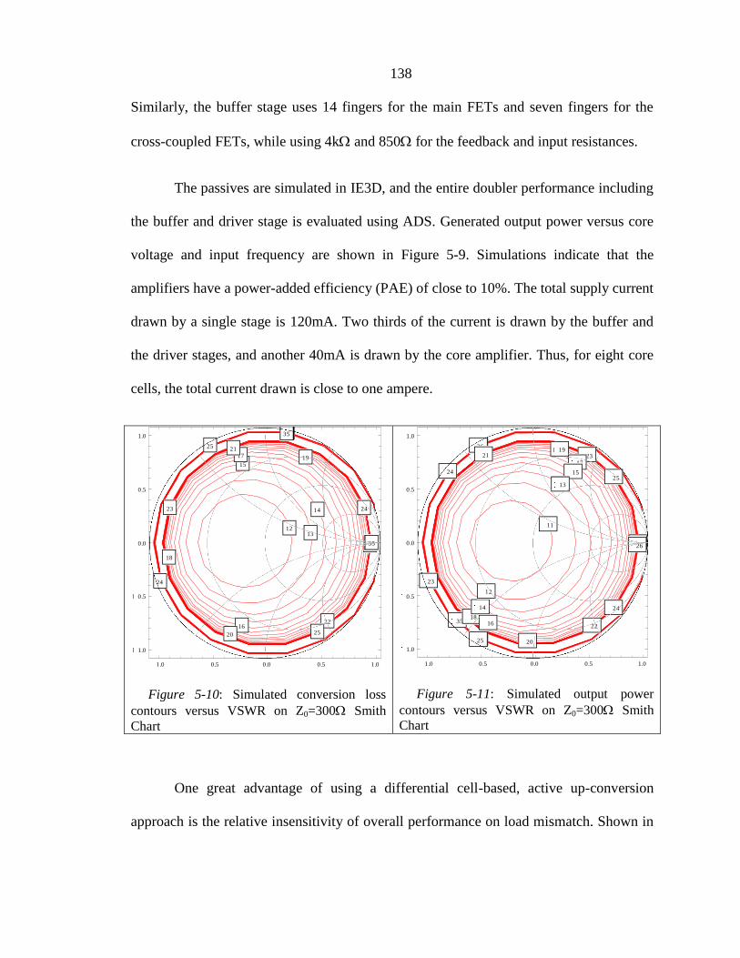
138
Similarly, the buffer stage uses 14 fingers for the main FETs and seven fingers for the
cross-coupled FETs, while using 4k and 850 for the feedback and input resistances.
The passives are simulated in IE3D, and the entire doubler performance including
the buffer and driver stage is evaluated using ADS. Generated output power versus core
voltage and input frequency are shown in Figure 5-9. Simulations indicate that the
amplifiers have a power-added efficiency (PAE) of close to 10%. The total supply current
drawn by a single stage is 120mA. Two thirds of the current is drawn by the buffer and
the driver stages, and another 40mA is drawn by the core amplifier. Thus, for eight core
cells, the total current drawn is close to one ampere.
Figure 5-10: Simulated conversion loss
contours versus VSWR on Z0=300 Smith
Chart
Figure 5-11: Simulated output power
contours versus VSWR on Z0=300 Smith
Chart
One great advantage of using a differential cell-based, active up-conversion
approach is the relative insensitivity of overall performance on load mismatch. Shown in
1213
14
15
16
17
18
19
20
21
22
23
24
24
25
25
26
26
27
27
28
28
29
29
30
30
31
31
32
32
32
32
33
33
34
34
35
35
1.0 0.5 0.0 0.5 1.0
1.0
0.5
0.0
0.5
1.0
35
35
34
34
33
33
32
32
31
31
30
30
29
29
28
28
27
27
26
26
25
2524
24
23
23
22
21
20
19
18
17
16
15
14
13
12
11
1.0 0.5 0.0 0.5 1.0
1.0
0.5
0.0
0.5
1.0

139
Figure 5-10 and Figure 5-11 are simulated conversion loss and output power contours
plotted on a Smith chart (Z0=300) to illustrate this point.
Section 5.3.3 – Phase Rotating VCO Designs
The purpose of the phase-rotating VCOs cells is twofold: (1) they provide phase-
control for the core cells, as they allow a digitally controllable phase-shift as the
reference signal progresses across the chip, and (2) they provide amplitude restoration for
the reference signal as a means to keep the fundamental signal power constant across the
chip.
Two possible phase rotator design were investigated. The initial design
considered uses the architecture used by Wang [69] and the design of such a stage was
completed including substantial layout. However, several disadvantages of this design
approach became so pronounced that this alternative was abandoned in favor of a design
that employs a locked VCO. The main disadvantages of the approach used by Wang are
power consumption, low gain and difficulty of providing and routing two signals in
quadrature to the core cells. Because gain is at a premium, and the current steering
architecture wastes gain by using effectively larger than required transistors, the entire
phase rotator cell using the Wang architecture provided almost no power gain in
simulation. Furthermore, the required layout size and power consumption was large
enough, to be of concern, particularly when layout parasitics were included in the
performance simulations.
Thus, the approach was abandoned, and an approach using phase-locked VCOs
was chosen. The main disadvantage of the phase-locked approach is that it requires a

140
sufficiently strong locking signal and that the output amplitude is not fully controllable.
However, these disadvantages were deemed to put the overall design at less risk than the
Wang approach, since the VCO approach consumes much less power and only requires a
single phase reference signal.
Because the achievable phase shift at the fundamental frequency is less than the
theoretically achievable (and hence less than at the second harmonic), two
phase shifters are employed per core cell half (and, and hence four total per core cell).
One phase shifter is placed adjacent to the input of the core cell, while the second is
placed approximately in the center between different cells.
Figure 5-12: Core cell schematic including phase shifters and routing details.
The schematic of the design so far is shown in Figure 5-12. The VCO phase
shifters are controlled by eight-bit DACs that set the control voltage. Depending on the
input frequency and the control voltage setting, different amounts of phase shift are
realized, as discussed in Section 5.2.2 – Element Amplitude and Phase-Control. The
Input A:
Pin @ fo
Differential
antenna:
Pout @ 2 fo
VCO
DAC
Input B:
Pin @ fo
TL
ine
TLine
VCO
DAC
TL
ine
TLine
x2
Doubler core 1
VCO
DAC DAC
x2
Digital controlVCO control voltage
Digital controlVCO control voltage
Fundamental flow, distribution
To core
To next cell
Doubler core 2

141
simulated phase shift is shown in Figure 5-13. At the edges of the operation frequency
range (at 121GHz), the achievable phase-shift per shifter can drop to a shift as low as 80o,
thus limiting the range of phase shift at the second harmonic with two phase shifters to
320o. The center of the operation frequency in simulation was purposefully chosen to be
slightly too high, since not all parasitics could be extracted and the remaining parasitics
were deemed to lower the center frequency slightly. The phase shifters draw 8mA from a
600mV supply. There are a total of 32 phase rotators on chip, drawing a total current of
256mA nominally.
The phase shifter amplifiers use fourteen fingers of 880m cross-coupled devices
for the VCO core, and a four finger device for signal injection on each side. The varactor
is fashioned out of regular enhancement-mode MOSFET devices. Even though depletion
mode MOSFETs were available in the design kit, their ultimate availability during tape-
out could not be established reliably with the foundry. Furthermore, even though the
enhancement-mode devices provide less tuning range and inferior performance, their
modeling at 125GHz was deemed to be more accurate. Two twenty-four finger devices
were connected back-to-back with the drain-source connection at the virtual ground node
serving as the control-voltage node. The bulk connection was provided separately
(dubbed “secondary” control voltage, Vcontrol,2) such that the bulk and the drain-source
wells can be controlled separately. This trick8 increases the available tuning range by a
couple of percent. The full schematic is shown in Figure 5-14.
8 Suggested by A. Hajimiri

142
Figure 5-13: Simulated output phase of
single phase-shifter for different frequencies
versus control voltage.
Figure 5-14: Schematic of phase rotator.
Section 5.3.4 – Signal Routing Amplifiers
The signal routing amplifier cells are located in front of and directly after the
phase-rotating VCOs. The amplification cell in front of the VCO ensures sufficient signal
strength to lock the phase-rotating VCO, while the amplifier after the VCO isolates the
phase-rotating VCO from the transmission line load, increasing the tuning range and
reference signal power. For the core cells, the output amplifier is split into two paths to
provide the driving signal for both the core cell buffer amplifier as well as the outgoing
transmission line. The amplifiers employ a spiral inductor load to tune out the various
device capacitances. The amplifiers are supplied from a separate supply and draw 20mA
each per set from a 0.65V nominal supply for a total of 580mA. They do not use any
cross-coupled devices.
Locking Range
Phase Shift:
0=
1
2
= 0
In+ In-
Vcontrol
Vcontrol,2
VDD
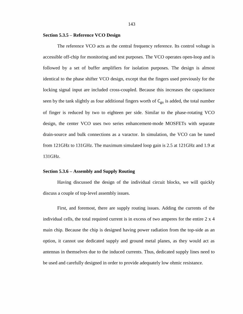
143
Section 5.3.5 – Reference VCO Design
The reference VCO acts as the central frequency reference. Its control voltage is
accessible off-chip for monitoring and test purposes. The VCO operates open-loop and is
followed by a set of buffer amplifiers for isolation purposes. The design is almost
identical to the phase shifter VCO design, except that the fingers used previously for the
locking signal input are included cross-coupled. Because this increases the capacitance
seen by the tank slightly as four additional fingers worth of is added, the total number
of finger is reduced by two to eighteen per side. Similar to the phase-rotating VCO
design, the center VCO uses two series enhancement-mode MOSFETs with separate
drain-source and bulk connections as a varactor. In simulation, the VCO can be tuned
from 121GHz to 131GHz. The maximum simulated loop gain is 2.5 at 121GHz and 1.9 at
131GHz.
Section 5.3.6 – Assembly and Supply Routing
Having discussed the design of the individual circuit blocks, we will quickly
discuss a couple of top-level assembly issues.
First, and foremost, there are supply routing issues. Adding the currents of the
individual cells, the total required current is in excess of two amperes for the entire 2 x 4
main chip. Because the chip is designed having power radiation from the top-side as an
option, it cannot use dedicated supply and ground metal planes, as they would act as
antennas in themselves due to the induced currents. Thus, dedicated supply lines need to
be used and carefully designed in order to provide adequately low ohmic resistance.

144
Five supply lines domains and one ground domain were allowed for. The supply
domains supply domains are for all VCO supplies (reference VCO and phase-
shifting VCOs) – nominally 0.55V – for the phase rotator buffer amplifiers
(nominally 0.6V), for the core buffer and driver amplifiers, for the primary
core amplifier (that provides signal power to the frequency doubler) – both nominally
0.73V – and finally for the DACs (1V nominally). This supply separation allows
better testability over different biasing conditions.
Cell Core Drivers Phase
Rotators/VCO
Distribution
Buffers
Digital
DACs
Nominal
Supply
Voltage
0.73V 0.73V 0.6V 0.65V 1.0V
Nominal
Supply
Current
8·40mA 16·40mA 34·8mA 33·20mA 33·2mA
Figure 5-15: Nominal supply voltages and currents
Nominally, the nominal currents drawn in each supply domain are listed in Figure
5-15. Because the currents are significant, differences in the ohmic resistance of the
supply rails can cause noticeable supply voltage differences. Hence, the resistances of the
various supply rails were carefully calculated during the layout to ensure similar values
and hence supply voltages. All supply lines are fed from the top and bottom on dedicated
pads such that routing distances can be most easily equalized. Ground supply lines are
routed in a similar fashion. In addition, the transmission line grounds are used locally to
also provide correct local RF signal referencing. However, because the transmission line
grounds are fairly narrow, side-walls were contacted where necessary. The center of the
chip contains a ground and supply line domain running perpendicular to the antenna

145
orientation to provide additional low-impedance DC paths particularly for the ground
currents since the ground domain needs to return the entire DC current. Calculated DC
voltage drops on supply and ground voltages were calculated to be up to 30mV each,
which is significant. Increased supply rail metal widths were deemed to interfere too
much with intended top-side radiation.
An additional top-level layout constraint was the direction of the reference signal
transmission lines as the daisy-chaining required the main direction to run in parallel to
the antenna direction. This will result in induced currents and interference with the
desired antenna pattern, but the interference is difficult to quantify using EM simulations
because of the problem size. Design time was also limited and because the option for
back-side radiation testing always existed, the routing was left as it is.
Section 5.4 – Experimental Results
Two test-chips are designed and taped-out in UMC’s 65nm standard CMOS
process, including thick top-layer metallization. A test-chip containing a 2x4 array and a
smaller, single-unit, 2x1 array test-chip were fabricated. Die photographs of the fully
bonded 2x1 and 2x4 chips are shown in Figure 5-16 and Figure 5-17, respectively.
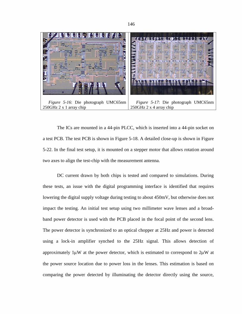
146
Figure 5-16: Die photograph UMC65nm
250GHz 2 x 1 array chip
Figure 5-17: Die photograph UMC65nm
250GHz 2 x 4 array chip
The ICs are mounted in a 44-pin PLCC, which is inserted into a 44-pin socket on
a test PCB. The test PCB is shown in Figure 5-18. A detailed close-up is shown in Figure
5-22. In the final test setup, it is mounted on a stepper motor that allows rotation around
two axes to align the test-chip with the measurement antenna.
DC current drawn by both chips is tested and compared to simulations. During
these tests, an issue with the digital programming interface is identified that requires
lowering the digital supply voltage during testing to about 450mV, but otherwise does not
impact the testing. An initial test setup using two millimeter wave lenses and a broad-
band power detector is used with the PCB placed in the focal point of the second lens.
The power detector is synchronized to an optical chopper at 25Hz and power is detected
using a lock-in amplifier synched to the 25Hz signal. This allows detection of
approximately 1W at the power detector, which is estimated to correspond to 2W at
the power source location due to power loss in the lenses. This estimation is based on
comparing the power detected by illuminating the detector directly using the source,

147
versus first collimating and refocusing the beams through the lenses. The absolute power
provided by the source is calibrated using an Erickson power meter, and varies
considerably and in the band from 220GHz to 300GHz. This variation is confirmed in the
detector setup as well, and is therefore unlikely due to impedance mismatch between the
multiplier output and the taper used to connect to the Erickson power meter. The setup is
calibrated using a VDI 220-300 GHz power source. Shown in Figure 5-19 is the setup,
without protective covers that are used during operation to isolate the power detector
from daylight. Using this setup, no power can be detected by the power detected as
radiated from the 250GHz IC.
Figure 5-18: 250GHz test-chip mounted in
PLCC socket on test PCB. The PCB is attached
to a stepper motor to allow rotation around two
axes shown (red arrows)
Figure 5-19: Lens-based detection setup,
shown here with calibration source
To investigate possible causes, supply voltages are increased until DC currents
drawn are closer to or even exceed values determined from simulation. In order to
investigate any DC biasing issues on chip, the local DC voltages are probed on-chip
using a DC probe needle. To gain access to the nodes, the passivation is locally removed
5V supply
connections
Core biasing
PCB
Core biasing
Antenna
pattern stepper
motor
44 pin
PLCC
+ IC
VDI multiplier-
based power
source
Millimeter wave
PE lenses
Power Detector
Optical Chopper

148
for most of the supply and ground connection to the various core, driver, phase rotator
and phase rotator buffer supplies. Since all of these supply lines are located on the top
aluminum redistribution metal layer or the thick copper layer underneath, accessing these
nodes is relatively simple, albeit work intensive (requiring measurement of
approximately 100 DC voltages per biasing option). The on-chip DC voltages are
measured on both the 1x2 and 4x2 test-chips under several supply biasing scenarios. An
example result is shown in Figure 5-20, where the different colors codify the different
circuit blocks. Here, red is the phase rotator buffer, yellow the phase rotator and VCO
blocks, and green the driver amplifier and core blocks. The top number in each box is the
voltage (in mV) as referenced to an off-chip ground, with the bottom number being the
voltage on the closest ground point.
From these measurements, several observations were made: First, the local DC
ground supply to the reference oscillator is high (in Figure 5-20 it is at 155mV compared
to the PCB ground!) because of a tight ground connection requiring significant DC
current to be conducted through the transmission line ground shield. A different bottle-
neck occurs at the ground connection for the blocks in the top-right corner of the chip (in
both the 1x2 as well as the 4x2 test-chips) because of an additional missing local DC
ground connection. These measurements were performed for several biasing scenarios for
both test-chips to ensure sufficient biasing to all circuit blocks. However, as a result some
asymmetry in DC biasing exists, particularly between top and bottom half of the IC as
was noticed during the DC measurements for the 4x2 test-chip.
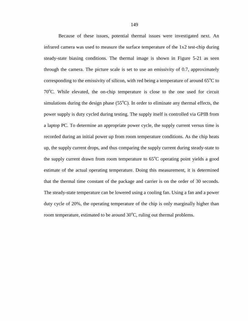
149
Because of these issues, potential thermal issues were investigated next. An
infrared camera was used to measure the surface temperature of the 1x2 test-chip during
steady-state biasing conditions. The thermal image is shown in Figure 5-21 as seen
through the camera. The picture scale is set to use an emissivity of 0.7, approximately
corresponding to the emissivity of silicon, with red being a temperature of around 65oC to
70oC. While elevated, the on-chip temperature is close to the one used for circuit
simulations during the design phase (55oC). In order to eliminate any thermal effects, the
power supply is duty cycled during testing. The supply itself is controlled via GPIB from
a laptop PC. To determine an appropriate power cycle, the supply current versus time is
recorded during an initial power up from room temperature conditions. As the chip heats
up, the supply current drops, and thus comparing the supply current during steady-state to
the supply current drawn from room temperature to 65oC operating point yields a good
estimate of the actual operating temperature. Doing this measurement, it is determined
that the thermal time constant of the package and carrier is on the order of 30 seconds.
The steady-state temperature can be lowered using a cooling fan. Using a fan and a power
duty cycle of 20%, the operating temperature of the chip is only marginally higher than
room temperature, estimated to be around 30oC, ruling out thermal problems.
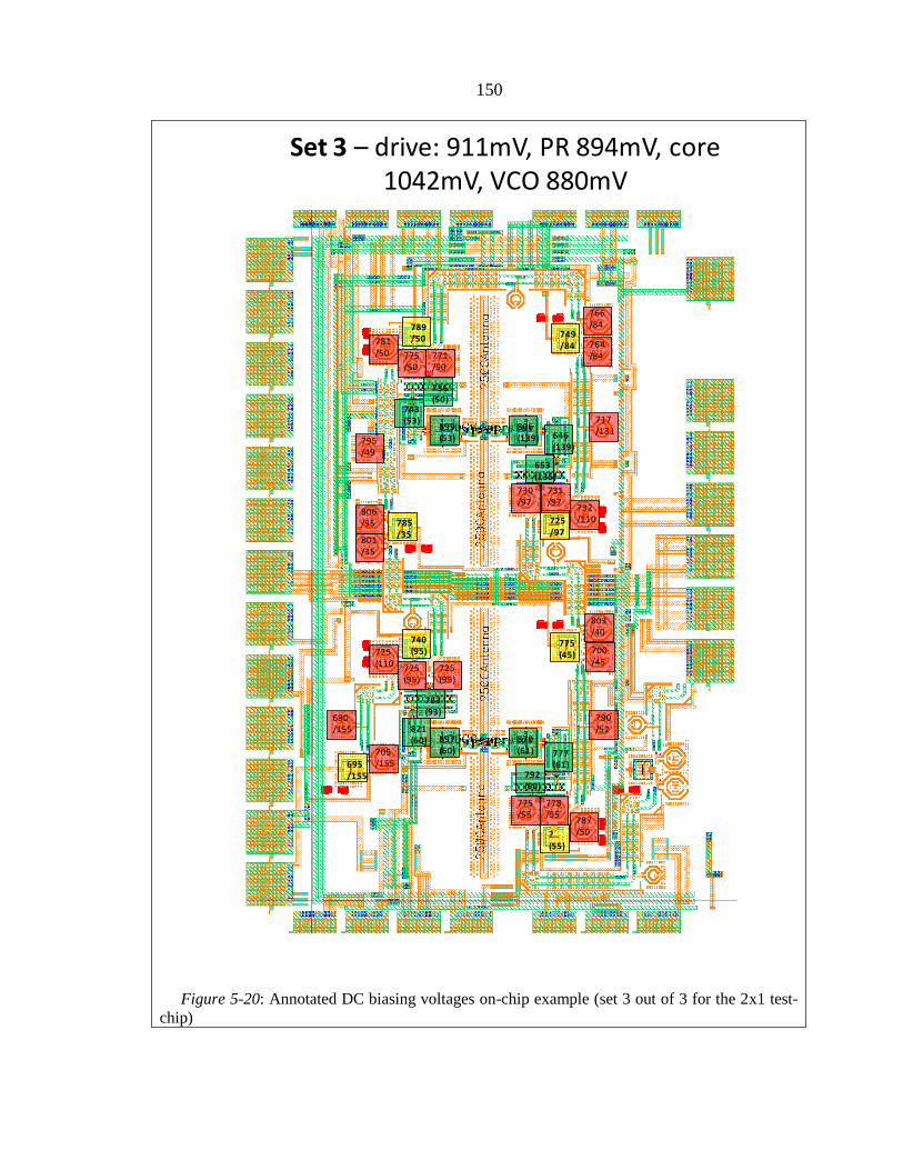
150
Figure 5-20: Annotated DC biasing voltages on-chip example (set 3 out of 3 for the 2x1 test-
chip)
Set 3 – drive: 911mV, PR 894mV, core 1042mV, VCO 880mV
763(93)
740(95)
695/155
821(60) 897
(60)705/155
690/155
725(110 725
(95)725(95)
725/97
806(139)
717/131
749/84
732/110
730/97
731/97
653(135)
646(139)
766/84
764/84
899(53)
743(53)
736(50)
775/50
771/50
781/50
795/49
806/35
801/35
785/35
789/50
870(61) 777
(61)792(60)
775/55
778/55
803/40
787/50
790/52
700/45
775(45)
?(55)

151
Figure 5-21: Thermal image of the 1x2
test-chip during steady-state biasing
conditions. The scale used with emissivity
set to that of silicon corresponds red being
around 65oC.
Figure 5-22: Close-up photo of 250GHz test-chip in
PLCC socket on PCB.
In order to obtain a more sensitive measurement of the radiated output power, a
Pacific Millimeter passive downconversion mixer is used. The mixer uses double-
balanced diodes and operates without a DC bias. The RF signal is captured directly from
air using a rectangular horn antenna with 25dB of directional gain. The downconversion
mixer is followed by a cascade of Mini-Circuits microwave amplifiers, and the down-
converted and amplified signal is detected using an Agilent E4448A Spectrum Analyzer.
The best sensitivity is obtained using a base-band signal at approximately 800MHz. A
photograph of the setup is shown in Figure 5-23. The setup is fully automated (with the
exception of the stepper motor). Power supplies, the Agilent E4448A Spectrum Analyzer
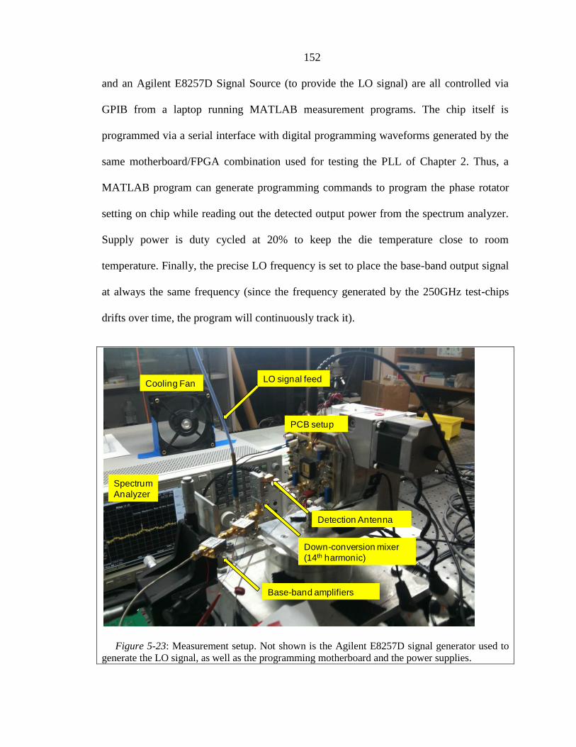
152
and an Agilent E8257D Signal Source (to provide the LO signal) are all controlled via
GPIB from a laptop running MATLAB measurement programs. The chip itself is
programmed via a serial interface with digital programming waveforms generated by the
same motherboard/FPGA combination used for testing the PLL of Chapter 2. Thus, a
MATLAB program can generate programming commands to program the phase rotator
setting on chip while reading out the detected output power from the spectrum analyzer.
Supply power is duty cycled at 20% to keep the die temperature close to room
temperature. Finally, the precise LO frequency is set to place the base-band output signal
at always the same frequency (since the frequency generated by the 250GHz test-chips
drifts over time, the program will continuously track it).
Figure 5-23: Measurement setup. Not shown is the Agilent E8257D signal generator used to
generate the LO signal, as well as the programming motherboard and the power supplies.
Cooling Fan
PCB setup
Detection Antenna
Spectrum
Analyzer
Down-conversion mixer
(14th harmonic)
Base-band amplifiers
LO signal feed

153
This advanced setup allows for accurate measurement of the radiated output
power over time and phase rotator programming settings. Because using the Pacific
Millimeter mixer allows more sensitivity, a free-space output signal is detected and can
be measured.
In order to determine the correct phase rotator settings, an automated search is
performed. Starting from an initial setting that produces a detectable output signal, the
phase rotator settings are varied to continuously increase the detected output power.
Several approaches are used to vary the phase rotator settings. Because each individual
measurement performed by the spectrum analyzer can exhibit considerable statistical
variation (up to one dB), multiple measurement must be performed for each setting. The
program used tries a list of different settings and measures each multiple times, recording
the average and the standard deviation. A student’s T-test is performed to determine
whether a particular setting performs statistically worse than the current best setting using
a predetermined confidence interval (typically 95%) until the best setting is identified.
For each round, then, a list of settings is tested. The list can typically include (1)
gradients on each phase rotator setting as well as (2) opposite polarity differential settings
on adjacent phase rotator pairs. Case (1) corresponds to a phase shift for all phase rotators
following the programmed one, while case (2) corresponds to approximately a change in
phase for only the current phase rotator (as the next phase rotator is programmed with a
step of opposite polarity, approximately offsetting the phase shift introduced by the
previous detector). Local minima can be avoided by selectively allowing individual
registers to be programmed across a large swath of settings.
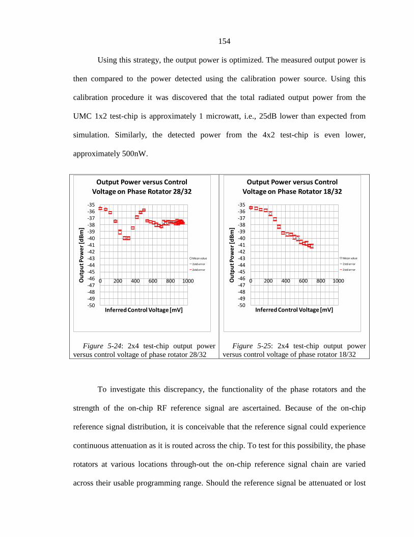
154
Using this strategy, the output power is optimized. The measured output power is
then compared to the power detected using the calibration power source. Using this
calibration procedure it was discovered that the total radiated output power from the
UMC 1x2 test-chip is approximately 1 microwatt, i.e., 25dB lower than expected from
simulation. Similarly, the detected power from the 4x2 test-chip is even lower,
approximately 500nW.
Figure 5-24: 2x4 test-chip output power
versus control voltage of phase rotator 28/32
Figure 5-25: 2x4 test-chip output power
versus control voltage of phase rotator 18/32
To investigate this discrepancy, the functionality of the phase rotators and the
strength of the on-chip RF reference signal are ascertained. Because of the on-chip
reference signal distribution, it is conceivable that the reference signal could experience
continuous attenuation as it is routed across the chip. To test for this possibility, the phase
rotators at various locations through-out the on-chip reference signal chain are varied
across their usable programming range. Should the reference signal be attenuated or lost
-50-49-48-47-46-45-44-43-42-41-40-39-38-37-36-35
0 200 400 600 800 1000Ou
tpu
t Po
we
r [d
Bm
]
Inferred Control Voltage [mV]
Output Power versus Control
Voltage on Phase Rotator 28/32
Mean value
2std error
2std error
-50-49-48-47-46-45-44-43-42-41-40-39-38-37-36-35
0 200 400 600 800 1000Ou
tpu
t Po
we
r [d
Bm
]
Inferred Control Voltage [mV]
Output Power versus Control
Voltage on Phase Rotator 18/32
Mean value
2std error
2std error

155
while traversing the chip, phase rotator settings after complete attenuation cannot have a
measurable effect on the detected output power. We check for this hypothesis using both
the 1x2 and 4x2 test-chips. The results for the 4x2 test-chip are shown for registers 18
(located close to the center) and register 28 (being the fourth to last one in the reference
distribution chain). The results are shown in Figure 5-25 and Figure 5-24, respectively.
As can be seen, the signal is lost in register 28 for control voltages greater than 500mV,
but from register 18 still exhibits good signal integrity, since the output power varies
continuously over the control voltage. Beyond register 28, the useful range of control
voltages is reduced further, likely due to the supply bottleneck in the phase rotator at that
location discussed earlier. For the 1x4 chip, the last register (register 8) is fully
programmable. Thus, while loss of signal integrity over the reference signal chain is an
issue, it is only an issue for the 2x4 chip for the very last registers, and – by itself –
cannot explain the reduced output power.
To further investigate the issue, antenna patterns are measured. For the 2x4 chip,
the exhibited pattern is very sharp, such that the signal drops off by more than 10dB
beyond a 20o angle from the bore-side. Because the initial signal-to-noise ratio is only
12dB or so to begin with, a pattern measurement is not really possible, but these values
do agree from what we would expect from simulations. However, we can measure the
pattern of the 1x2 test-chip in the elevation around the axis of the dipole antennas. The
result from simulation is shown in Figure 5-26. From the result, we would expect peak
radiation at 45o elevation, and nearly constant gain for elevation angles all the way to 70
o.
The inset in Figure 5-26 visualizes the 3-dimensional shape. The measurement results are
shown in Figure 5-27. By comparing Figure 5-26 with Figure 5-27, we can note that the
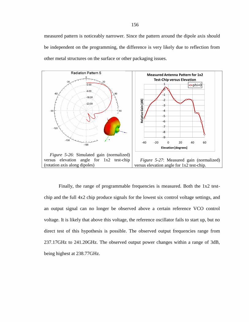
156
measured pattern is noticeably narrower. Since the pattern around the dipole axis should
be independent on the programming, the difference is very likely due to reflection from
other metal structures on the surface or other packaging issues.
Figure 5-26: Simulated gain (normalized)
versus elevation angle for 1x2 test-chip
(rotation axis along dipoles)
Figure 5-27: Measured gain (normalized)
versus elevation angle for 1x2 test-chip.
Finally, the range of programmable frequencies is measured. Both the 1x2 test-
chip and the full 4x2 chip produce signals for the lowest six control voltage settings, and
an output signal can no longer be observed above a certain reference VCO control
voltage. It is likely that above this voltage, the reference oscillator fails to start up, but no
direct test of this hypothesis is possible. The observed output frequencies range from
237.17GHz to 241.20GHz. The observed output power changes within a range of 3dB,
being highest at 238.77GHz.
-9
-8
-7
-6
-5
-4
-3
-2
-1
0
1
-40 -20 0 20 40 60R
ela
tive
Gai
n [d
B]
Elevation [degrees]
Measured Antenna Pattern for 1x2
Test-Chip versus Elevation
phi=0

157
Section 5.5 – Discussion and Conclusion
From the measurements, it appears that there is no single cause for the reduced
output power compared to simulation. A variety of possibilities exist: (1) the difference is
due to core losses or lower core efficiency, (2) the difference is due to insufficient signal
drive strength into the core circuitry, and (3) the difference is due to packaging issues and
(4) the difference is due to losses or problems related to reference signal distribution. It is
also possible (and even likely) that a combination of factors is responsible for the
observed difference.
The greatest challenge and risk factor in the design is the reliance on tuned
circuits involving passive structures, particularly in the drive chain as well as the core
circuitry. Test cut-outs were not implemented due to the unavailability of equipment in
the lab to measure performance of circuit primitives at 125GHz. Test cut-outs could have
served as a debugging tool for evaluation to check both whether (1) The core circuitry
drive chain is tuned correctly, and (2) the core circuitry drive chain has sufficient gain.
Another possibility is that the reference VCO signal is weak to start with, and
hence the drive circuits do not receive sufficient input power. This hypothesis is
somewhat supported by the observation that the reference VCO may not start up at higher
frequencies. Furthermore, the tuning range that is observed is relatively low considering
that 300mV of control voltage range is covered (it is lower than simulated). This may
indicate that additional parasitic tank capacitance exists (also supported by the fact that
the lowest frequency is several GHz lower than simulated), and that the VCO loop gain
may be lower to begin with. To test this hypothesis, a test-structure including an on-chip
158
mixer would be required that would allow to mix the VCO output to a lower frequency
that can be observed with the equipment available. Using such a test-structure, VCO
start-up issues and low output power issues could be identified. There is some
circumstantial evidence against this hypothesis, namely that if the VCO signal is weak to
begin with, and we would expect to see greater problems in the reference signal chain or,
alternatively, better signal strength towards the end of the reference distribution chain.
It is also possible that one or several circuits are mistuned. However, if most of
the detuning occurred in a single component, we would expect a strong output power-
versus-frequency slope, which we do not observe. The only alternative is that two circuits
are detuned in an opposite fashion (that is, one too high, and the other too low), to
produce maximum output power for an intermediate frequency. While not impossible,
this scenario is deemed rather unlikely just because it would involve two incorrect
electromagnetic and/or parasitic simulation results resulting in errors of opposite signs.
Since the same CAD tools have been used throughout the design, this possibility seems
unlikely.
Finally, we need to consider the possibility that severe packaging problems are
present. In particular, if the effective die thickness is substantially different from the ideal
die thickness, losses in excess of 10dB can be easily occurred. Similarly, the additional
metal structures on-chip such as pads and transmission lines, which are impossible to
fully include in electromagnetic simulations, may contribute a significant loss factor due
to reflections or antenna pattern changes. This hypothesis could be tested using a
different package design. This would require back-lapping of the current IC and design of

159
a new back-side radiation package (for example a test platform using a silicon lens). If
the output power issues were due to packaging issues, significantly more power should be
observed.
In summary, a second spin tape-out designed to test these hypotheses in detail
could provide further insight. The design of a radio front-end beyond fmax of the device
is a challenging proposal since it requires many separate parts to work together in
harmony for the system to perform optimally.

160
Chapter 6 – Taking Integrated High-
Frequency Radio Design to the Next
Dimension
Section 6.1 – Problems and Opportunities in Integrated Circuit
Antenna Design
As previously discussed in Section 5.2.1 – Antenna Array Design, the design of
fully integrated circuit antennas presents the designer with problems inherent to the
physics of electromagnetic radiation. First and foremost, the permittivity of bulk silicon
(approximately ) results in most of the electromagnetic energy to be coupled
preferentially into the silicon substrate rather than the surrounding air. The designer, then,
has several options, all of which have some inherent disadvantage associated with them.
One possibility is to introduce an additional ground plane that prevents the
electromagnetic energy from deeply penetrating the substrate. However, because of the
planar processing of integrated circuits, separation between different metal layers is on
the order of ten micrometer or less. The metal layers themselves are typically located in a
separate dielectric layer (silicon dioxide in CMOS), with permittivity of approximately
. Thus, even a ten micrometer dielectric layer corresponds to one fiftieth of a
wavelength at 300GHz and is thus electromagnetically thin. Placing a ground layer ten
micrometers away from an antenna is equivalent to placing an identical antenna twenty
micrometers away that is driven at opposite polarity by the Method of Images (see e.g.,
[73]). The result is a significant reduction in the radiation resistance, resulting in a
significant reduction in the radiation efficiency due to conduction losses in the antenna
161
metal [62]. This problem can be addressed using integrated patch antennas (e.g., [74]).
However, patch antennas suffer from small bandwidths and narrow radiation patterns and
thus require careful design.
Instead of fashioning the ground plane from the top-metal layers, the integrated
circuit package itself can be used, as the die is typically attached to a ground plane.
However, a dielectric substrate with a ground plane supports various guided modes that
will be excited. These substrate modes will not radiate (or radiate from the side of the
integrated circuit die), and thus lower the overall radiation efficiency. The number and
types of modes excited is a function of the substrate thickness used [62], and thus the
substrate thickness introduces another design parameter that needs to be carefully
adjusted, with radiation efficiencies lower due to these modes.
To remove the constraint of exciting substrate modes, the radiation can be emitted
from the substrate backside. This can be accomplished using a dielectric lens [60] [59]
[75] (optionally with a quarter-wave impedance matching layer) that utilizes the fact that
most of the energy is radiated into the substrate and can thus be focused using a lens
made of the substrate material. This approach, however, has the disadvantage that the
package requires the lens. Furthermore, additional dissipative losses in the dielectric
material need to be controlled since the silicon lens will introduce losses as well as the
integrated circuit substrate. An alternative approach is to directly radiate from the
backside without a lens [50]. An integrated circuit antenna on an ungrounded substrate
generally excites fewer substrate modes [59], but can still complicate the assembly.

162
Because of the aforementioned issues, the design of integrated circuit antennas is
still considered an active area of research with potentially a wide array of applications.
Section 6.2 – Three-Dimensional Antenna Design in Integrated
Circuit – A Paradigm Shift
At this point, we would like to take a broader view at the problem of integrating
antennas. In the most general form, the problems arise because of physical and
processing constraints. The planar structure of integrated circuits – in a most general
sense – only allows us to control the electromagnetic boundary conditions on a bounded
plane at the surface of the semiconductor material. Furthermore, the use of a single or a
few available material configurations (such as a single material on a grounded substrate
in a typical package) further constrains the problem. This second constraint is very likely
going to play less of a role going forward, as commercial packaging solutions are moving
towards solutions offering multiple dies and multiple materials. This development is
driven by the ever increasing demands of system integration whereby multi-component
reference designs that previously were assembled on a PCB can now be delivered in
integrated packages that combine multiple die on a variety of substrate materials, greatly
simplifying the system design and reducing the time-to-market for the end-user.
Furthermore, three-dimensional assemblies of integrated circuits are becoming
commonplace for low form-factor products such as memory modules and smart-phones
among others. A striking illustration of the advances made is shown in Figure 6-1, where
a packaged stack of nineteen dies including wire-bonds is depicted.

163
What has been proposed [1] is a paradigm shift in integrated circuit design
interfacing the physical world, away from a classical planar integrated design towards a
more holistic approach. This approach emphasizes finding solutions to problems using
the entire design space, both physical and electronic, fully utilizing a vertical approach
that solves problems holistically on all design levels (from devices to package) rather
than in the traditional top-down approach.
Figure 6-1: Multi-die stack packaging solution, offered by Amkor Technologies [76]
As insinuated, one way to approach problems of integrated circuit antennas in
particular, and electromagnetic interaction with the physical environment in general, is to
employ fully three-dimensional arrangements of circuits and elements to overcome
boundaries set by traditional, two-dimensional design approaches.
Amkor Technology

164
In the following sections, this concept will be explored using 3-dimensional
integrated circuit structures available using die stacks as shown in Figure 6-1. We will
first explain the mathematical approach taken to solve these three-dimensional combined
electromagnetic and electronic problems, and then develop and explore a variety of
possible applications. We will conclude this chapter with a summary and an outlook.
Section 6.3 – Design of 3-Dimensional Antenna Structures –
Mathematical Approach
In this section, we will describe the approaches taken to design and optimize 3-
dimensional electromagnetic structures. We will first formulate the problem setup, and
then describe a practical software implementation to investigate and solve these
problems.
Figure 6-2: Side and top view of dipole test
structure. +/- indicate sides of a driving
terminal.
Figure 6-3: Optimal structure shape
determination using software approach
+ -
Antenna driving port
Test terminals
Antenna Metal(s)
Side view
Top view
+ -+ -+ - + - + - + -+ -
Test terminals Test terminals
Antenna driving port
Optimization of terminal loads
+ -+ - + - + -
+ -
+ -
General test-shape with configurable terminals
+ -+ - + - + -+ -
+ -+ - + - + -+ -
+ -+ - + - + -+ -
Optimal shape deduced from terminal
configuration

165
Section 6.3.1 – Design Approach
The design of a multi-layered electromagnetic element array, for example an
antenna array, requires the design of both a suitable configuration and arrangement of
electromagnetic elements – such as the shapes of metallic surfaces and the choice and
thickness of dielectric layers among others – as well as suitable terminations, either active
drives or passive terminations. Several of these parameters have to be determined using
iterative approaches and the designer’s insight and experience into and with the particular
problem. Several others of these variables are amenable to automation.
In particular, the loading and driving requirements of terminals within the
structure can be effectively automated, and for a particular set of problems it can be
shown that the required optimization can be cast as a convex optimization, which modern
numerical software packages can easily and effectively handle. For shaping of metallic
surfaces and structures that are terminated and/or driven by the circuit, we can often gain
insight using the same tools, by simulating a particular structure template and
approximating the problem of designing the particular, optimal shape of the structure
using variable terminal elements connecting parts of the structure to obtain insight into
sizing and shaping (as illustrated in Figure 6-2 and Figure 6-3). In this way, the
electromagnetic optimization has been recast as a problem of extracting a circuit model
with variable terminations, and the optimization is performed over the terminations.
An example easily illustrates this approach: assuming the goal is to optimize the
length of a particular dipole element within a given physical surrounding, instead of
simulating n variations of dipoles, all of different lengths, we instead simulate a dipole of

166
some length, and introduce ports connecting different pieces of the dipole across its
length. An electromagnetic solver can extract a linear circuit model (with ports
– the last for the antenna drive) and the terminals can be loaded with impedances to
simulate and optimize, for example, the driving point impedance. Terminations that are
or approach short circuits then yield the result that these terminations should just be
shorted, open circuit terminations indicate to get rid of the extra length and intermediate
terminations can give feedback about appropriately shortening or lengthening sections.
Figure 6-2 illustrates this approach. The optimization then would load the “test terminals”
with short circuits, open circuits or arbitrary reactances while optimizing the “antenna
driving port” to be as close as possible to some desired driving point impedance.
For a general structure then, an electromagnetic simulation is performed to obtain
a linear circuit model, and a linear circuit solver/optimization tool is used to optimize the
driving or loading at particular test ports. For antenna problems in particular, the goal is
to direct power through the network in a favorable way, such that a constraint is set up by
which the power received at certain terminals is kept constant (either zero or some finite
value), while the power admitted to the driving terminals is minimized (for example to
obtain maximum radiation efficiency in a certain radiation direction, or to guide power
flow through a substrate).
Section 6.3.2 – Problem Formulation
Given a (passive) linear network with terminals, the first terminals are driven
by a voltage source, and terminals are terminated by a general impedance (possibly
constrained to a certain subset of all impedances, such that . The power
167
transmitted is the sum power injected into the network by voltage sources,
∑ . of the terminals are designated receive ports, such that the real part of the
port impedance is positive and the power received is recorded, possibly with an
associated weight, such that ∑ . Of interest is the maximization of the
quantity ⁄ .
We solve the problem using an s-parameter representation of the linear network.
Let and
be the forward and reflected voltage waves on the ith
port. Then,
;
√ ;
√ (6-1)
normalized to a reference impedance . The voltage on and current into the ith
port is
then
( )√ (6-2)
and,
( )
√
(6-3)
To describe the problem in matrix form suitable for solving in a commercial math
package (e.g., Matlab). We define a vector
[
] (6-4)
that contains the forward and reverse voltage waves. We, then, can express the set of
linear equations for the voltages and impedances as

168
[
] ; [ ] (6-5)
Here, is an by one column vector for the voltages on the voltage ports, and and
are by diagonal matrices with the first diagonal elements being √ and the
remaining diagonal elements being where is the impedance of the load on
the ith
port, i.e.,
[
√
] (6-6)
The latter set of equations simply solves
( )
( ) (6-7)
Since some of the variables are voltages and some are impedances, we define the solution
column vector , composed of the real part of the voltages, the real part of the load
impedances, the imaginary part of the voltages and the imaginary part of the impedances,
in that order.
We use auxiliary matrices , and to translate to a voltage vector
(using ) and also into the matrix ( ) ( ).
( ) is a diagonal matrix with as the diagonal elements, and
169
[
] [
] (6-8)
Also,
[
] (6-9)
During the optimization, an automatic program maximizes
(6-10)
and and are diagonal matrices with ones on the diagonal for the receive ports
or transmitting ports, respectively.
A Matlab program has been written to solve the above problem (optimizing the
efficiency) using the toolbox routine fmincon, a non-linear optimization tool. The
maximization is achieved by minimizing the negative of the efficiency above. The
program calculates the gradient, the Hessian, and the Lagrangian of the two matrices
( ) ( )
( ) ( ) and ( (
) ( ) ( )
( ) )
to improve convergence speed and stability, as well as to allow constraining the
parameters for subsets of . Constraints are also used to exclude degenerate solutions
(same excitations, rotated phases, for example).
An important subset of this problem has only one receiving element, terminated
with constant impedance, and all remaining terminals are driven by voltage sources.
Then, the power received is constant if the voltage over the receiving element is constant.
170
The power admitted to the network by the voltage sources is inversely proportional to
, thus minimizing it maximizes . The voltage over the receiving element is kept
constant using a linear constraint. The problem can then be cast into a quadratic program
of the form
( ( )
( ) ) (6-11)
with an additional linear constraint
( ( ) ) (6-12)
This problem is convex because the eigenvalues of the matrix in parentheses are all
positive, and fast quadratic program implementations exist, such as quadprog in Matlab
(also compare [77]).
Section 6.3.3 – Implementation
The above formulation can be used to implement software solvers that can
optimize the desired quantities. In particular, several MATLAB programs were
implemented, most notably a quadratic program solver and a general non-linear solver.
The quadratic program solver solves problems of the type where one receiving element
exists, with all other elements being driven by ideal voltage sources. The program reads
in the EM circuit description from a standard Touchstone format file and solves the
quadratic program using MATLAB’s quadprog library routine. A second program using
MATLAB’s fmincon library routine to minimize the transmit efficiency is implemented
as well.

171
Section 6.4 – Application Studies for 3-Dimensional Antenna
Structures
In this section, a variety of possible applications for the technique complete with
simulation results are presented.
Section 6.4.1 – Integrated, Beam-forming Antenna Arrays
When designing integrated circuit antennas on silicon substrate, the substrate
dimensions and surroundings can greatly constrain the achievable performance due to the
existence of substrate modes as well as radiation leakage from the sides of the substrate.
In particular, good efficiency can typically be achieved when relatively thin substrates are
chosen such that only few substrate modes exist. However, the cutoff frequency of the
first dielectric substrate mode, both for grounded and floating substrates, is at DC, and
the thin substrate leads to constraints on the directionality that can be achieved as the
power excited in the mode leaks out in undesired directions.
In other cases, certain substrate heights can be extremely disadvantageous for
radiation at particular frequencies using certain antenna primitives such as dipole
antennas. To illustrate this point, the length of a single dipole antenna on a grounded,
lossless Si substrate is optimized in length using Zeland’s IE3D (an electromagnetic
solver software package) radiation efficiency solving capabilities for various substrate
heights. The result is plotted in Figure 6-4 (black curve). Plotted also are the cutoff
frequencies for the various substrate modes as well. As can be seen, for a 250 micron
substrate, certain frequencies cannot be efficiently radiated using dipole antennas of any
length located on top of the substrate. The location of these frequencies varies as the

172
height of the antenna is varied within in the substrate as can also be noted in Figure 6-4.
Since the only loss mechanism present in this setup are excited substrate modes, we
conclude that dipole shaped antennas at different heights within the substrate excite the
substrate modes in a different fashion.
This point is highlighted in the following simulation: at each of the desired
frequencies, the optimal antenna length determined from the previous simulation is used
in a 5x1 array on an infinite silicon substrate placed on a ground plane. For the 2-
dimensional case, only antennas on the top-surface are used, whereas for the 3-
dimensional case, antennas are placed additionally at 50m intervals in height. The
driving voltage of the antennas is optimized to achieve maximum bore-side radiation (via
a single test antenna placed at bore-side). The result is shown in Figure 6-5. Most notably
in this example, the 3D antenna array can be used at frequencies for which the substrate
height results in strong substrate mode excitation, and hence low radiation efficiency.
This also highlights the fact that by using an array in the 2D case compared to a single
dipole antenna cannot provide significant improvement over the single antenna case
(compare Figure 6-4) as the notch of at 350GHz is still present even in the array case.
Shown also in Figure 6-5 in broken lines are the predictions made for the antenna gain in
the bore-side direction by the MATLAB solver tool (since the starting point is known
from the initial simulation, and a predicted gain can be deduced by the improvement
during numerical optimization). The solid lines were obtained by resimulating the
structure using the particular solution obtained. At most frequencies the result is close to
the numerical prediction, except at 500GHz. This highlights some of the limitations of
this design approach as the EM solvers typically assume that all terminals are terminated

173
in some impedance and numerical approximations used by the solvers lead to different
solutions for different termination/excitation scenarios (because otherwise the solution
should be unchanged).
The mere presence of metal structures affects the solution and this is a problem
that makes the design of such structures more difficult using the approach by which part
of the structure is optimized using a circuit model. For example, the previous 3D
simulation is rerun, but this time half of the antennas are removed, leading to a sparser
array, but higher numerical accuracy. As shown in Figure 6-6, the gain achieved at
500GHz is now high in the somewhat sparser case, even though the problem is similar in
structure.
The previous simulation results are corroborated using a finite silicon substrate
(this time lossy with resistivity of 10 cm) and a different simulator (Ansoft HFSS). The
general simulation setup for the 3-D case is shown in Figure 6-7 (with the sense antenna
at a 45o angle). The antenna gain in the bore-side and towards 45
o elevation is optimized
for the 2D and 3D cases, again using antennas of optimal lengths at each frequency. The
results versus frequency for these two cases are shown in Figure 6-8 and Figure 6-9. The
3D array thus provides better directionality over frequency than the 2D array. Noticeable
is the greatly improved performance in the 2D, finite substrate case shown here compared
with the 2D, infinite substrate case presented previously, as the substrate modes are now
apparently reflected from the side-walls, and their energy partially redirected since the
“trough” around 350GHz is greatly reduced, particularly for radiation toward 45o
elevation.

174
The improvement in directionality can also be observed from the radiation
patterns produced in the 2D and 3D cases with radiation patterns shown for optimization
towards 45o elevation at different azimuths is shown in Figure 6-10 through Figure 6-15
as the patterns are more sharply defined and generally spread less across the azimuth
angles away from 0o.
To summarize, using 3-dimensional structures for building antenna arrays can
potentially offer improvements in efficiency and directionality.
Figure 6-4: Radiation efficiency, optimal
dipole in 250 micron Si lossless substrate at
height z (top of Si at z=250 micron)
Figure 6-5: Antenna gain of 2D (blue) and
3D (red) dipole array as simulated (solid) and
predicted (broken).
-30
-25
-20
-15
-10
-5
0
200 250 300 350 400 450 500 550 600
Rad
iati
on
loss
[d
B]
Frequency [GHz]
Radiation efficiencies vs antenna
Z-position
Z=250uZ=200uZ=150uZ=100uZ=50u
TE2 TM2 TE3 TM3
-20
-15
-10
-5
0
5
200 250 300 350 400 450 500
Up
wa
rds
gain
[d
Bi]
Frequency [GHz]
IE3D, antenna gain (f=0o), 2D/3D cases, optimized drive + prediction,
250u infinite Si
2D (opt)
2D (pred)
3D (opt)
3D (pred)

175
Figure 6-6: Antenna gain resimulated for 3D
case using sparser array.
Figure 6-7: HFFS simulation setup for
simulating 2D and 3D antenna arrays (3D
shown)
Figure 6-8: Bore-side array gain optimized
for 2D, 3D cases
Figure 6-9: 45o elevation gain optimized for
2D, 3D cases
-20
-15
-10
-5
0
5
200 250 300 350 400 450 500
Up
wa
rds
gain
[d
Bi]
Frequency [GHz]
IE3D, antenna gain (f=0o), 3D/3D sparse cases, optimized drive +
prediction, 250u infinite Si
3D, sparse (opt)
3D, sparse (pred)
3D (opt)
3D (pred)
0
2
4
6
8
10
200 250 300 350 400 450 500
up
war
d g
ain
[d
Bi]
Frequency [GHz]
q=0o (upward radiation), 2D (planar) versus 3D (bulk) case
3D antenna array
2D antenna array 0
2
4
6
8
10
250 300 350 400 450 500 550
up
war
d g
ain
[d
Bi]
Frequency [GHz]
q=45o (upward radiation), 2D (planar) versus 3D (bulk) case
3D antenna array
2D antenna array
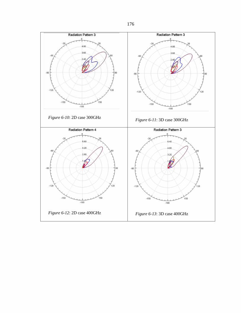
176
Figure 6-10: 2D case 300GHz
Figure 6-11: 3D case 300GHz
Figure 6-12: 2D case 400GHz
Figure 6-13: 3D case 400GHz

177
Figure 6-14: 2D case 500GHz
Figure 6-15: 3D case 500GHz
Figure 6-16: Normalized antenna gain
versus frequency for center driven reflectarray.
Figure 6-17: Antenna gain versus
frequency, active drive (impulse like)
excitation.
Section 6.4.2 – Frequency-tunable Antenna Structures
As discussed in the previous section, using the third dimension can help extend
frequency coverage for given substrate thicknesses. A related application is that of a
frequency-tunable antenna. There are many applications, for which control over the
-16
-14
-12
-10
-8
-6
-4
-2
0
200 250 300 350 400 450 500
No
rmal
ized
An
ten
na
Gai
n [
dB
]
Frequency [GHz]
Passive element array, optimized for
different frequencies, 3D versus 2D
3D-450G2D-450G3D-350G2D-350G3D-250G2D-250G
178
center frequency can be useful. For example, tuning the center frequency of an antenna
can allow a single antenna structure to be used for a multi-band radio. Normally, multiple
antennas are required to cover multiple frequency ranges, whereas a single, tunable
antenna structure is preferable as it can also be adjusted in situ, leading to applications
that may be defined as software controlled antennas.
Related applications have been discussed by Babakhani [78] and Lavaei [79],
where the directionality of an antenna can be adjusted using tunable reflectors, or even
multiple directions can be targeted at the same time. Furthermore, Babakhani discusses
applications where the signal is modulated using the tunable array such that the
modulation is meaningful only in a particular transmit direction. Using the third
dimension to shape or otherwise influence the radiation pattern can also benefit these
known applications.
For this discussion, 2D and 3D structures similar to that in Figure 6-7 are used
where the antenna length this time is fixed and optimized for radiation at 450GHz. Only
the center antenna at the top surface is used as an active radiator in the first simulation.
The remaining elements are tuned reactively. Figure 6-16 shows the normalized antenna
gain with the normalization done such that the maximum gain in the upwards direction is
0dB. All solid lines are results for the bulk structure and all broken lines are results for
the traditional planar structure. Different colors are used for the different tunings (i.e.,
changes in reactive loads on all but the top-center element) such that the top-center
element accepts maximum radiation from the upward direction at a particular center
frequency in the 250-450GHz frequency range. We note that the three-dimensional bulk

179
structure provides superior contrast and full usability over the frequency range, whereas
the traditional, planar structure has low contrast due to multiple peaks and reduced range
as it cannot distinguish signals from 250GHz to 350GHz (broken yellow and green lines).
Using the disclosed technique, we have provided a straightforward way of
implementing a frequency-selective receiver, which could be useful for spectroscopic
applications, for example. In particular, the center element could use a wide-band power
detector and the side and bulk elements only need to implement reactively tuned elements
(for example using varactors, which are available with reasonable quality factors even in
current, high-volume commercial semiconductor processes) to implement a frequency-
tunable power detector.
In another experiment, the array is actively driven in such a way that each element
is excited by an impulse of varying amplitude and phase (but such that the amplitude of
the excitation is the same at all frequencies and that the phase lead/lag increases
proportionally with frequency). Amplitudes and phases at each element are optimized to
maximize radiation straight up at 250GHz, 350GHz, and 450GHz. Figure 6-17 shows the
result. The amplitudes applied are rounded off to within +/-5% of the center antenna
amplitude. Very little contrast is achieved for the traditional planar case, whereas using
bulk elements again provides vastly superior contrast.
Section 6.4.3 – Programmable, Quasi-optical Functional Blocks
In this section, we will discuss other examples that emphasize electromagnetic
near-field manipulation to further illustrate the strength of introducing buried

180
electromagnetic elements in the substrate, and to demonstrate the great potential scope of
this new technique.
Because physical optics is an application of electromagnetic theory, we can
borrow from it to obtain ideas for implementing the functionality of such devices using
electronics instead. Two examples of such devices are electronically manipulated shutters
and reflectors (or mirrors), in other words structures that are transparent or reflective to
incoming radiation. Those structures could be used to guide radiation within the substrate
or through the substrate interface. For example a shutter could be used to block or trap
energy inside the substrate (by reflecting energy back) until it is “opened,” that is made
transparent.
Figure 6-18: Electronically tunable
guidance through silicon
Figure 6-19: 2D guided radiation case. Top:
maximum radiation, bottom: maximum dielectric
guidance
To illustrate the above, an HFSS simulation is set up as follows: A slab of
lossless, silicon bulk material of 250m thickness is placed on a conducting ground
z
x
y
5.05mW
4.98mW (73uW sensed in desired direction)
6.13uWz
x
y
5.05mW
4.97mW radiated
63.4uW

181
plane, and two dipole antennas are placed inside, one on each end. These dipoles, at a
depth of 125m, are test dipoles to excite and sense electromagnetic energy flow inside
the substrate (approximately 65% of the energy excites substrate modes in this setup).
Between the two dipoles an electromagnetic element array is located. We simulate two
cases: in the first case (traditional) only elements on the top-surface are used, in the
second case, bulk elements as part of this invention are used. The elements in the array
are manipulated passively only, that is, they do not absorb or radiate energy and, in
tandem, act as a reconfigurable reflector. Figure 6-18 shows the simulation setup, with
the red circle highlighting the guiding elements and the black circle highlighting the
transmit and receive elements. Additional sense antennas are used in free-space
surrounding the materials to monitor radiation (see below). Radiation to the bulk or sense
antennas are maximized or minimized by adding reactively tuned loads to the
electromagnetic elements.
First, reactive loading of the elements is chosen to maximize the energy sensed by
the air sensors while the energy to the bulk sensing antenna is minimized. For the planar
case, 5.05mW input power results in 4.98mW radiated power (with 66.9W sensed by
the air sensors) and 6.1W sensed by the bulk sensor. Figure 6-19 (top) shows a cartoon
of the energy flow in this setup. Since the bulk is (nearly) lossless, the majority of the
energy is eventually radiated. Next, reactive loading of the elements in the same setup is
chosen to maximize energy flow to the bulk sensor. In this case, the bulk sensor senses
63.4W with 4.97mW radiated. The budget is shown in Figure 6-19 (bottom). While
63.4W sensed in the bulk corresponds to a ten-fold increase in directed power compared

182
the previous case, it still is only 1.25% of the total power submitted. In a lossless 250m
Si substrate of infinite extent with a ground plane, a half-wavelength dipole at 125m
depth radiates 65% of the power into the substrate. Hence, 3.28mW is (initially) kept in
the substrate and 1.77mW is radiated. Of the 3.28mW, 63.4W is captured, and 81.9W
is lost in the substrate, which is 2.5% of the power initially submitted into the substrate.
This implies that the free path of the substrate power not absorbed is 2.5% of the mean
free path. Hence, most of the energy leaves the substrate sooner rather than later. In other
words, the surface elements only have a marginal effect on the substrate modes and
cannot prevent a large fraction of the power from leaving the substrate.
Figure 6-20 : 3D guided radiation case. Top:
maximum radiation, bottom: maximum dielectric
guidance
Figure 6-21: Planar 2D arrangement for
electronically tunable guidance through
silicon
An entirely different situation occurs for the setup that uses bulk elements. Power
radiated along the directions of the sense antennas (off-chip) is maximized first. The
z
x
y
3.21mW
2.865mW radiated
131nW
z
x
y
4.07mW
2.02mW radiated
1.59mW

183
power flow diagram is shown in Figure 6-20 (top). Submitted power is 3.21mW, with
95.8W detected at the sense antennas (3% of the submitted power sensed versus 1.4%
sensed in the 2D planar case, corresponding to approximately 3dB higher directivity
towards the sense antennas). The bulk sensor receives 131nW, corresponding to 0.04% of
the power submitted compared to 0.12% in the 2D planar case. The lower overall
efficiency compared to the 2D planar case is significant as it corresponds to a larger flow
path length inside the substrate.
Using the bulk element setup to direct the energy towards the bulk sensors, the
results in the power flow are shown in Figure 6-20 (top). Of the 4.07mW submitted,
1.59mW is absorbed in the bulk sense antenna, and 2.02mW is radiated into air. Because
only 65% of the power is directed towards bulk modes, 1.4mW of the 2.02mW would
have been radiated in any case (since the element array is several wavelengths away) and
that the additional “spill-over” radiation is as low as 600uW. This demonstrates
significant mode conversion by the bulk array to a mode that the bulk sense antenna can
use.
Simulations for an alternative “planar” arrangement have been performed (using a
vertical arrangement, compare Figure 6-21. Performance is similar to the planar case
discussed, with only slightly improved control over the horizontal planar case. For
direction into air, submitted power is 5.50mW with 97.8% radiated, 486nW bulk sensed
power and 58.1W sensed air power. For maximal bulk directivity, 7.37mW is submitted
with 219.4W sensed at the bulk sensor and overall 95.7% radiation radiated. Hence, the

184
improved guidance is due to being able to control the bulk of the substrate compared to a
single surface (whether horizontal or vertical).
As demonstrated, using bulk elements in a full-3D arrangement, one can
implement programmable reflectors with significantly improved directivity compared the
two-dimensional planar case. Because all manipulation was accomplished using reactive
tunings only, reprogrammable structures that can selectively reflect, entrap and/or direct
the flow of energy can be implemented using the disclosed technique.
Figure 6-22: Dielectric box, 2D control
surface, entrapment mode.
Figure 6-23: Dielectric box, 2D control
surface, radiation mode
Many possible applications are imaginable, with one discussed in the remainder
of this section to further illustrate using the disclosed technique to implement
electronically manipulated reflectors to direct the flow of electromagnetic energy. We
will discuss a source that uses the semiconductor bulk to selective trap energy inside the
semiconductor bulk or, alternatively, radiate it. This may be useful for the construction of

185
a pulses source that could store and selectively release electromagnetic energy to the
surrounding. To illustrate this idea, a traditional, planar dipole array and a 3D-bulk dipole
array are simulated, both implemented in a lossy (1S/m), 250um thick piece of silicon on
a ground plane, as illustrated in Figure 6-7 for the 3D case. The top-center element in
both cases is driven to supply power (at 450GHz), and the remaining elements are
reactively tuned to selectively entrap energy in the substrate (“storage mode”) or radiate
energy upwards (“radiation mode”). In the traditional planar case, during storage-mode,
the input source provides 124.6W, of which 60.6% is radiated into air due to imperfect
containment. The input impedance seen at the source is 20.2+111.5j, corresponding
to a quality factor of 5.5 (the ratio of energy stored versus energy dissipated). The power
detected at the air sensor is 88.4nW. Switching to radiation-mode, input power increases
to 253.2W, the input impedance seen changes to 43+107.8j (quality factor of 2.5)
and radiation efficiency changes to 88.9% with 2.84W sensed at the sensor, an increase
of 15dB. From the radiation pattern, the gain in the upward direction changes from -
3.2dB to 5.8dB (the sense antenna aperture shields some of the outgoing radiation).Figure
6-22 and Figure 6-23 show the radiation patterns in both cases. Note the significant
amount of power leakage to the sides in Figure 6-22.

186
Figure 6-24: Dielectric box with 3D
control over radiation/entrapment. Here, the
radiation pattern for the entrapment mode is
shown.
Figure 6-25: Dielectric box with 3D control
over radiation/entrapment. Here, the radiation
pattern for the radiation mode is shown.
For the three-dimensional bulk case, in the storage mode, the input power is
63.3uW and power sensed is 17.7nW. Input impedance is 8.5+102.9j, corresponding
to a quality factor of 12. The radiation efficiency is 24.1%. Therefore, significantly more
energy is stored in the bulk and leakage radiation is reduced significantly compared to the
planar case. This is also obvious from the radiation pattern, shown in Figure 6-24, when
compared to the pattern in Figure 6-22 (both figures use identical coloring scheme).
Switching to radiation mode, the sensor now registers 7.74W with 323.9W input
power. The antenna gain increases from -7.3dB to 9.62dB in the upward direction
compared to the storage-mode. The input impedance is 45.2+95.2j, corresponding to
a quality factor of 2. The radiation pattern is shown in Figure 6-25. The higher directional
gain, the larger contrast between storage- and radiation mode (compared to the planar
case), as well as the increase in energy that can be stored in the bulk (as evidenced by the

187
larger quality factor in storage mode) illustrate the usefulness of the bulk technique for
implementing actively manipulated reflectors (to keep the energy in the bulk).
Because the electromagnetic simulation tools only provide steady-state solutions,
it is difficult to predict time-transient behavior since that requires knowledge of delay in
the system. However, we note that delay is related to the physical size of the system and
that applications that employ the bulk as an energy storage element are imaginable. For
example, when the timing of switching between states is aligned with the delay in the
system, a pulsed source could be implemented that can provide higher instantaneous
power by utilizing the stored energy. The specifics depend on the horizontal and vertical
dimensions of the bulk.
To summarize, in this section we have demonstrated that our technique can be
used to influence the electromagnetic near-field to reflect, trap or block the flow of
electromagnetic energy for the purpose of achieving desirable electromagnetic near- and
far-fields. As demonstrated, traditional, planar techniques are very inadequate for the
same purpose. Many applications not specifically discussed are imaginable that employ
our invention to implement shutters, reflectors, and flow-directors. This technique is
obviously not limited to the examples given, and many other exciting possibilities exist,
for example programmable lenses or mode-coupling devices to name two.
Section 6.5 - Outlook
In this chapter, we have generalized the problem of integrated circuit antenna
design to a general class of problems that require integrated circuits to interact
electromagnetically with the physical environment. Using a holistic design paradigm, we

188
have used three-dimensional arrangements of circuits, antennas and materials to explore
possible solutions and applications to some of these problems with the help of a custom
linear circuit solver that allows mathematical optimizations to be performed within the
design space. Besides potentially providing novel solutions to existing applications, this
approach may open up a whole new set of new applications, previously unobtainable
using traditional integrated circuit approaches. We believe that the ideas presented here
will open new avenues for integrated circuit and system design.

189
Chapter 7 – Summary and Closing
Remarks
Section 7.1 – Thesis Summary
In this dissertation, the design of several micro- and millimeter-wave signal
generation, transmitter and radio systems was presented. These designs were motivated
by advances made recently in modern communication electronic systems and applications
and semiconductor fabrication technology – particularly CMOS. The designs were
complemented and further motivated by theoretical considerations. Finally, a new
paradigm for designing integrated electromagnetic structures was proposed and explored
with the help of commercial as well as custom simulation tools.
In particular, a novel technique for using closed-loop feedback to mitigate
spurious output tones in integrated phase-locked loop synthesizers was developed and
experimentally verified. We have illuminated the causes and mitigation of spurious
output tones in detail, and presented a first proof-of-concept design based on the
developed background. Our approach is orthogonal to approaches found in the literature
can be implemented independently of known other approaches.
Furthermore, the generation of millimeter wave signals in integrated circuit
processes in general, and modern digital CMOS processes in particular, was developed,
starting from theoretical considerations, and complemented using measurements and

190
simulations. These considerations can serve as a foundation for millimeter wave and
terahertz system design in CMOS processes in the future.
Two millimeter wave systems were designed and tested. While the results still
deviate from the simulated performance, they explored important design considerations
for larger integrated radio systems, and a lot has been learned that is applicable to future
designs. Some possible avenues can still be explored in measurement to further advance
the knowledge of millimeter wave system design in integrated CMOS processes.
In the final chapter, a new paradigm for designing electromagnetic interfaces in
integrated circuits has been proposed based on the more general paradigm of holistic
integrated circuit design [1]. In our new paradigm, we employ multiple assembled
dielectric substrates (either made of semiconductor material or even other dielectric
substances) and circuits on those substrates to control the electromagnetic near-field in
three physical dimensions rather than the two dimensions available in traditional design
methodology. We have investigated several possible applications and believe that many
more as of yet unexplored possibilities exists, opening an exciting opportunity for novel
research.
Section 7.2 – Potential Further Work
Before concluding this dissertation, we would like to briefly describe possibilities
for future work arising from the work presented here.
As mentioned previously, our closed-loop spurious tone reduction scheme could
be fully integrated with an on-chip custom digital ASIC for feedback control. Reductions

191
in the sensing and actuation component of the circuit are possible, and additional
actuation channels could be integrated. Further testing of the available circuits could
focus on automatic digital (FPGA-based) feedback control as well as further testing of
the FM demodulation capabilities.
Further testing performed on the 250GHz and 500GHz test-chips could provide
additional insights useful for future testing and development.
Finally, applications and implementations for integrated three-dimensional
electromagnetic structures and systems could be developed and implemented. In
particular, I believe that a tunable millimeter wave detector could be a first step towards a
broad-band, integrated, millimeter wave spectrum analyzer.
Section 7.3 – The Future of Integrated Sub-Millimeter Wave
and Terahertz Radio
I would like to conclude this thesis with a statement of faith: as other authors [58]
[56], we believe that in the future terahertz systems and applications – particularly using
integrated semiconductor fabrication technologies – will gain far wider traction. While an
argument can be made that this is unlikely to occur since terahertz and millimeter wave
systems have been around for a while (albeit not in a very widespread fashion), we
believe that at some point in the future the momentum and available technology will
advance beyond a critical point after which applications for millimeter wave and terahertz
become widely accessible and distributed, similar to the spread of modern smart-phones
that started out similarly in a far ago age of XT personal computing technology and 1G

192
mobile phone technology (Figure 7-1, Figure 7-2). We hope we have contributed to the
state-of-the-art to bring this point a little closer to the present.
Figure 7-1: 1G phone, happy user (Dr.
Martin Cooper). Taken from http://mm-content-
blah.blogspot.com/
Figure 7-2: I-phone 3GS, considered
state-of-the-art in 2010. Taken from: http://www.apple.com/iphone/iphone-3gs/
193
Bibliography
[1] A. Hajimiri, "mm-Wave Silicon ICs: an Opportunity for Holistic Design," in
IEEE Radio-Frequency Integrated Circuits Symposium 2008, Digest, Atlanta,
2008.
[2] H. de Bellescize, "La réception Synchrone," L'Onde Electrique, vol. 11, pp.
230-240, 1932.
[3] S. Haykin, Communication Systems, 4th ed., John Wiley and Sons, 2001.
[4] W. Gruen, "Theory of AFC Synchronization," Proceedings of the IRE, vol.
41, no. 8, pp. 1043-1048, 1953.
[5] D. Richman, "Color-Carrier Reference Phase Synchronization Accuracy in
NTSC Color Television," Proceedings of the IRE, vol. 42, no. 1, pp. 106-133,
1954.
[6] C. Weaver, "A New Approach to the Linear Design and Analysis of Phase-
Locked Loops," IRE Transactions on Space Electronics and Telemetry, Vols.
SET-5, no. 4, pp. 166-178, 1959.
[7] J. Carson, "Notes on the theory of modulation," Proceedings of the IRE, vol.
10, no. 2, pp. 57-82, 1922.
[8] E. Armstrong, "A Method of Reducing Disturbances in Radio Signaling by a
System of Frequency Modulation," Proceedings of the IRE, vol. 24, no. 5, pp.
689-740, 1936.
[9] D. E. Foster and S. W. Seeley, "Automatic tuning, simplified circuits, and
design practice," Proc. of the Institute of Radio Engineers, vol. 25, no. 3, pp.
289-313, March 1937.
[10] S. W. Seeley, "Frequency Variation Response Circuits". United States Patent

194
2121103, 21 June 1938.
[11] B. Razavi and J. Sung, "A 2.5-Gb/sec 15-mW BiCMOS Clock Recovery
Circuit," in Symposium on VLSI Circuits, Digest of Technical Papers, Chapel
Hill, 1995.
[12] P. Zhang, L. Der, D. Guo, I. Sever, T. Bowdi, C. Lam, A. Zolfaghari, J.
Chen, D. Gambetta, B. Cheng, S. Gower, S. Hart, L. Huynh, T. Nguyen and B.
Razavi, "A CMOS Direct-Conversion Transceiver for IEEE 802.1la/b/g W L A
N s," in IEEE Custom Integrated Circuits Conference (CICC) 2004, 2004.
[13] H. Rategh, H. Samavati and T. Lee, "A CMOS frequency synthesizer with
an injection-locked frequency divider for a 5-GHz wireless LAN receiver,"
IEEE Journal of Solid-State Circuits, vol. 35, no. 5, pp. 780-787, May 2000.
[14] M. Banu and A. Dunlop, "A 660Mb/s CMOS Clock Recovery Circuit with
Instantaneous Locking for NRZ Data and Burst-Mode Transmission," in IEEE
International Solid-State Circuits Conference (ISSCC) 1993, Digest, 1993.
[15] A. Hajimiri, "Noise in Phase-Locked Loops," in 2001 Southwest Symposium
on Mixed-Signal Design, Austin, 2001.
[16] A. Mehrotra, "Noise Analysis of Phase-Locked Loops," IEEE Transactions
on Circuits and Systems - I, vol. 49, no. 9, pp. 1309-1316, September 2002.
[17] in The Design of CMOS Radio-Frequency Integrated Circuits, 1st ed.,
Cambridge University Press, 1998, pp. 71-75.
[18] N. Margaris and P. Mastorocostas, "On the Nonlinear Behavior of the
Analog Phase-Locked Loop: Synchronization," IEEE Trans. Industrial
Electronics , vol. 43, no. 6, pp. 621 - 629 , 1996.
[19] J. Nichols, "Frequency Distortion of Second- and Third-Order Phase-Locked
Loop Systems Using a Volterra-Series Approximation," IEEE Trans. Circuits
and Systems I, vol. 56, no. 2, pp. 453-459, 2009.
[20] F. Gardner, "Charge-Pump Phase-Lock Loops," IEEE Transactions on
Communications, vol. 28, no. 11, pp. 1849-1858, 1980.
[21] J. P. Hein and J. W. Scott, "z-Domain Model for Discrete-Time PLL's,"
IEEE Transactions on Circuits and Systems, vol. 35, no. 11, November 1988.
195
[22] R. Schreier and G. C. Temes, Understanding Delta-Sigma Data Converters,
1st ed., Wiley-IEEE Press, 2004, p. 464.
[23] X. Gao, E. Klumperink, M. Bosali and B. Nauta, "A Low Noise Sub-
Sampling PLL in Which Divider Noise is Eliminated and PD/CP Noise is Not
Multiplied by N^2," IEEE Journal of Solid-State Circuits, vol. 44, no. 12, pp.
3253-3263, 2009.
[24] S. Jeon, Y. Wang, H. Wang, F. Bohn, A. Natarajan, A. Babakhani and A.
Hajimiri, "A Scalable 6-to-18 GHz Concurrent Dual-Band Quad-Beam Phased-
Array Receiver in CMOS," IEEE Journal of Solid-State Circuits, vol. 43, no.
12, December 2008.
[25] F. Bohn, W. H., A. Natarajan, J. S. and H. A., "Fully integrated frequency
and phase generation for a 6-18GHz tunable multi-band phased-array receiver
in CMOS," in Radio Frequency Integrated Circuits Symposium, RFIC 2008,
Digest, Atlanta, 2008.
[26] F. Bohn, K. Dasgupta and A. Hajimiri, "Closed-loop spurious tone reduction
for self-healing frequency synthesizers," in Radio-Frequency Integrated
Circuits Conference, RFIC 2011, Digest, Baltimore, 2011.
[27] P. Larsson, "A 2-1600-MHz CMOS Clock Recovery PLL with Low-Vdd
Capability," IEEE Journal of Solid-State Circuits, vol. 43, no. 12, pp. 1951-
1960, Dec. 2000.
[28] K. Wang, A. Swaminathan and I. Galton, "Spurious tone suppression
techniques applied to a wide-bandwidth 2.4GHz fractional-N PLL," IEEE
Journal of Solid-State Circuits, vol. 43, no. 12, pp. 850-859, 2008.
[29] C.-F. Liang, S. H. Chen and S.-. I. Liu, "A Digital Calibration Technique for
Charge Pumps in Phase-Locked Systems," IEEE J. Solid-State Circuits, vol. 43,
no. 2, pp. 390-398, Feb. 2008.
[30] C.-Y. Kuo, J.-. Y. Chang and S.-. I. Liu, "A Spur-Reduction Technique for a
5-GHz Frequency Synthesizer," IEEE Trans. Circuits Syst. I, vol. 53, no. 3, pp.
526-533, Mar 2006.
[31] X. Gao, E. A. Klumperink, G. Socci, M. Bohsal and B. Nauta, "Spur
Reduction Techniques for Phase-Locked Loops Exploiting A Sub-Sampling
Phase Detector," IEEE J. Solid-State Circuits, vol. 45, no. 9, pp. 1809-1821,
196
Sep 2010.
[32] V. Kroupa, "Noise Properties in PLL Systems," IEEE Transactions on
Communications, Vols. COM-30, no. 10, pp. 2244-2252, 1982.
[33] B. Zhang, P. Allen and J. Huard, "A fast switching PLL frequency
synthesizer with an on-chip passive discrete-time loop filter in 0.25um CMOS,"
IEEE Journal of Solid-State Circuits, vol. 38, no. 6, pp. 855-865, 2003.
[34] K. Wang and I. Galton, "A Discrete-Time Model for the Design of Type-II
PLLs with Passive Sampled Loop Filters," IEEE Transactions on Circuits and
Systems - I, vol. 58, no. 2, pp. 264-275, Feb 2011.
[35] C. Vaucher, "An Adaptive PLL Tuning System Architecture," IEEE Journal
of Solid-State Circuits, vol. 35, no. 4, pp. 490-502, 2000.
[36] C.-F. Liang, H.-H. Chen and S.-I. Liu, "Spur-Suppression Techniques for
Frequency Synthesizers," IEEE Transactions on Circuits and Systems - II, vol.
54, no. 8, pp. 653-657, August 2007.
[37] C. Charles and D. Allstot, "A Calibrated Phase/Frequency Detector for
Reference Spur Reduction in Charge-Pump PLLs," IEEE Transactions on
Circuits and Systems - II, vol. 53, no. 9, pp. 822-826, September 2006.
[38] J. Choi, W. Kim and K. Lim, "A Spur-Suppression Technique Using an
Edge-Interpolator for a Charge-Pump PLL," IEEE Transactions on Very Large
Scale Integration Systems, 2011.
[39] C. Thambidurai and N. Krishnapura, "Spur Reduction in Wideband PLLs by
Random Positioning of Charge Pump Current Pulses," in 2010 IEEE
International Symposium on Circuits and Systems (ISCAS), 2010.
[40] C. Vaucher, I. Ferencic, M. Locher, S. Sedvallson, U. Voegeli and Z. Wang,
"A family of low-power, truly-modular programmable dividers in standard
0.35um CMOS technology," IEEE Journal of Solid-State Circuits, vol. 35, no.
7, pp. 1039-1045, 2000.
[41] A. Demir, "Computing Timing Jitter from Phase Noise Spectra for
Oscillators and Phase-Locked Loops with White and 1/f Noise," IEEE
Transactions on Circuits and Systems - I, vol. 53, no. 9, pp. 1869-1884, 2006.
197
[42] C.-H. Jan and e. al., "RF CMOS Technology Scaling in High-K/Metal Gate
Era for RF SoC (System-on-Chip) Applications," in 2010 IEEE Electron
Devices Meeting, 2010.
[43] A. Cathelin, B. Martineau, N. Seller, F. Gianesello, C. Raynaud and D.
Belot, "Deep-Submicron Digital CMOS Potentialities for Millimeter-Wave
Applications," in IEEE Radio Frequency Integrated Circuits Symposium, 2008.
[44] C. Tang, "An Exact Analysis of Varactor Frequency Multipliers," IEEE
Transactions on Microwave Theory and Technique, vol. 14, no. 4, pp. 210-212,
1966.
[45] E. Bava, G. Bava, A. Godone and G. Rietto, "Analysis of Varactor
Frequency Multipliers: Non-linear Behavior and Hysteresis Phenomena," IEEE
Transactions on Microwave Theory and Technique, vol. 27, no. 2, pp. 141-147,
1979.
[46] T. Leonard, "Prediction of Power and Efficiency of Frequency Doublers
Using Varactors Exhibiting a General Non-Linearity," Proceedings of the
IEEE, vol. 51, no. 8, pp. 1135-1139, 1963.
[47] D. Roberts and K. Wilson, "Evaluation of High Quality Varactor Diodes,"
The Radio and Electronic Engineer, vol. 31, no. 5, 1966.
[48] D. H., T. LaRocca, L. Samoska, A. Fung and M.-C. Chang, "324GHz
CMOS Frequency Generator Using Linear Superposition Technique," in IEEE
International Solid-State Circuits Conference 2008, Digest, San Francisco,
2008.
[49] K. Sengupta and A. Hajimiri, "Distributive Active Radiation for Terahertz
Signal Generation," in IEEE International Solid-State Circuits Conference
2011, Digest, San Francisco, 2011.
[50] I. T. R. f. Semiconductors, "www.itrs.net," [Online]. Available:
www.itrs.net. [Accessed 2011].
[51] H. Li, B. Jagannathan, J. Wang, T.-C. Su, S. Sweeney, J. Pekarik, Y. Shi, D.
Greenberg, Z. Jin, R. Groves, L. Wagner and S. Csutak, "Technology Scaling
and Device Design for 350GHz RF Performance in a 45nm Bulk CMOS
Process," in 2007 Symposium on VLSI Technology Digest of Technical Papers,
2007.
198
[52] J. Kraus and R. Marhefka, Antennas for All Applications, 3rd ed., McGraw-
Hill, 2001.
[53] C. Balanis, Antenna Theory, 3rd ed., John Wiley & Sons, 2005.
[54] K. Button, Ed., Infrared and Millimeter Waves, New York: Academic Press,
1981.
[55] I. Hosako, N. Sekine, M. Patrashin, S. Saito, K. Fukunaga, Y. Kasai, P.
Baron, T. Seta, J. Mendrok, S. Ochiai and H. Yasuda, "At the Dawn of a New
Era in Terahertz Technology," Proceedings of the IEEE, vol. 95, no. 8, pp.
1611-1623, July 2007.
[56] U. Pfeiffer, E. Öjeforsa, A. Lisauskasb, D. Glaabb, F. Voltolinac, V. Fonkwe
Nzogangc, P. Haring Bolívarc and H. Roskosb, "A CMOS Focal-Plane Array
for Terahertz Imaging," in 33rd International Conference on Infrared,
Millimeter and Terahertz Waves, Digest, 2008.
[57] E. Seok, D. Shim, M. C., R. Han, S. Sankaran, C. C., W. Knap and K. O,
"Progress and Challenges Towards Terahertz CMOS Integrated Circuits," IEEE
Journal of Solid-State Circuits, vol. 45, no. 8, pp. 1554-1564, Aug 2010.
[58] D. Rutledge and e. al., "Integrated-Circuit Antennas," in Infrared and
Millimeter Waves, New York, Academic, 1983, pp. 1-90.
[59] A. Babakhani, D. Rutledge and A. Hajimiri, "mm-Wave Phased Arrays in
Silicon with Integrated Circuit Antennas," in IEEE International Symposium
Antenna and Propagations Society 2007, Digest, 2007.
[60] Y. Su, J. Jau Lin and K. Kenneth, "A 20 GHz CMOS RF down-converter
with an on-chip antenna," in 2005 IEEE International Solid-State Circuits
Conference, Digest, San Francisco, 2205.
[61] D. Pozar, Microwave Engineering, 3rd ed., John Wiley & Sons, Inc., 2005.
[62] N. Alexopoulos, P. Katehi and D. Rutledge, "Substrate Optimization for
Integrated Circuit Antennas," in IEEE Microwave Theory and Technique
Symposium, Digest, Dallas, 1982.
[63] S. C. Cripps, RF Power Amplifiers for Wireless Communications, 2nd ed.,
Artech House, 2006.
199
[64] T.-P. Hung, D. Choi, L. Larson and P. Asbeck, "CMOS Outphasing Class-D
Amplifier With Chireix Combiner," IEEE Microwave and Wireless Component
Letters, vol. 17, no. 8, pp. 619-621, August 2007.
[65] J.-G. Kim, D.-W. Kang, B.-W. Min and G. Rebeiz, "A Single-Chip 36-
38GHz 4-Element Transmit/Receive Phased-Array with 5-bit Amplitude and
Phase Control," in IEEE International Microwave Symposium 2009, Digest,
2009.
[66] J. Buckwalter and A. Hajimiri, "An Active Analog Delay and the Delay
Reference Loop," in IEEE Radio-Frequency Integrated Circuits Conference,
2004.
[67] A. Natarajan, A. Komijani, X. Guan, A. Babakhani and A. Hajimiri, "A 77-
GHz Phased-Array Transceiver With On-Chip Antennas in Silicon: Transmitter
and Local LO-Path Phase Shifting," IEEE Journal of Solid-State Circuits, vol.
41, no. 12, pp. 2807-2819, Dec 2006.
[68] H. Wang and A. Hajimiri, "A Wideband CMOS Linear Digital Phase
Rotator," in IEEE 2007 Custom Integrated Circuits Conference (CICC), 2007.
[69] A. Mirzaei, M. E. Heidari and A. A. Abidi, "Analysis of Oscillators Locked
by Large Injection Signals: Generalized," in IEEE Custom Integrated Circuits
Conference (CICC) 2006, 2006.
[70] R. Adler, "A study of locking phenomena in oscillators," Proceedings of the
I.R.E., vol. 34, pp. 351-357, 1946.
[71] A. Hajimiri, H. Hashemi, A. Natarajan, X. Guan and A. Komijani,
"Integrated Phased Array Systems in Silicon," Proceedings of the IEEE, vol.
93, no. 9, pp. 1637-1655, Sep 2005.
[72] J. Jackson, Classical Electrodynamics, 3rd ed., Wiley, 1998.
[73] V. Radisic, S. Chew, Y. Qian and T. Itoh, "High-Efficiency Power Amplifier
Integrated with Antenna," IEEE Microwave and Guided Wave Letters, vol. 7,
no. 2, pp. 39-41, 1997.
[74] A. Babakhani, A. Komijani, A. Natarajan and A. Hajimiri, "A 77-GHz
Phased-Array Transceiver with On-Chip Antennas: Receiver and Antennas,"
IEEE Journal of Solid-State Circuits, vol. 41, no. 12, pp. 2795-2806, 2006.

200
[75] "Amkor Technology," [Online]. Available:
http://www.amkor.com/go/packaging/all-packages/3d-and-stacked-die-
packaging-technology-solutions/3d-and-stacked-die-packaging-technology-
solutions. [Accessed 2010].
[76] J. Lavaei, A. Babakhani, A. Hajimiri and J. Foyle, "Solving Large-Scale
Hybrid Circuit Antenna Problems," IEEE Transactions on Circuits and Systems
- I, vol. 58, no. 2, pp. 374-387, Jan 2011.
[77] A. Babakhani, J. Lavaei, J. Doyle and A. Hajimiri, "Finding Globally
Optimum Solutions in Antenna Optimization Problems," in International
Symposium of Antennas and Propagation Society (APSURSI), 2010.
[78] J. Lavaei, A. Babakhani, A. Hajimiri and J. Doyle, "Passively Controllable
Smart Antennas," in IEEE Global Communications Conference 2010
(GLOBECOM 2010), 2010.
[79] S. O. C.M. Bender, Advanced Mathematical Methods for Scientists and
Engineers, New York: Springer-Verlag New York, Inc., 1999.
[80] A. Demir, A. Mehrotra and J. Roychowdhury, "Phase Noise in Oscillators: A
Unifying Theory and Numerical Methods for Characterization," IEEE
Transactions on Circuits and Systems - I, vol. 47, no. 5, pp. 655-674, May
2000.