Insulated Gate Nitride-Based Field Effect Transistors
43
379 Abstract “Polarization doping” related to the piezoelectric and spontaneous polari- zation induced electric fields in nitride-based (III-N) semiconductors and large con- duction and valence band discontinuities at the heterointerfaces in these materials enable extremely high sheet carrier densities in device channels. As a consequence, insulated gate III-N field effect transistors are quite tolerant of the interface states at semiconductor-dielectric interfaces. High breakdown fields of III-N materials allow achieving high power operation, and superior transport properties of nitride semi- conductors make them suitable for high frequency operation. We describe materi- als growth, deposition and fabrication technology, device characteristics, reliability, and applications of insulated gate III-N field effect transistors and discuss future trends in this technology development. 13.1 Introduction AlN/GaN/InN materials system has unique properties that enable the development of superior electronic and optoelectronic devices, including Metal Oxide Semicon- ductor Field Effect Transistors (MOSFETs), Metal Oxide Semiconductor Heter- ostructure Field Effect Transistors (MOSHFETs), Metal Insulator Semiconductor Field Effect Transistors (MISFETs) and Metal Insulator Heterostructure Field Effect Transistors (MISHFETs). For semiconductors in this materials system, the energy gap varies from 6.2 eV for AlN to 3.4 eV for GaN and 0.65 eV for InN, allowing for great flexibility in the energy band engineered structures [1]. Polarization dop- ing [2, 3] allows for achieving extremely high carrier concentrations in the device channel without introducing dopants and related defects. The sheet carrier concen- tration in the GaN-based device channel can easily exceed 10 13 cm −2 and could be S. Oktyabrsky, P. D.Ye (eds.), Fundamentals of III-V Semiconductor MOSFETs, DOI 10.1007/978-1-4419-1547-4_13, © Springer Science+Business Media LLC 2010 Chapter 13 Insulated Gate Nitride-Based Field Effect Transistors M. Shur, G. Simin, S. Rumyantsev, R. Jain and R. Gaska M. Shur () ECSE Department and Broadband Center, Rensselaer Polytechnic Institute, Troy, NY 12180, USA e-mail: [email protected]
Transcript of Insulated Gate Nitride-Based Field Effect Transistors

379
Abstract “Polarization doping” related to the piezoelectric and spontaneous polari-zation induced electric fields in nitride-based (III-N) semiconductors and large con-duction and valence band discontinuities at the heterointerfaces in these materials enable extremely high sheet carrier densities in device channels. As a consequence, insulated gate III-N field effect transistors are quite tolerant of the interface states at semiconductor-dielectric interfaces. High breakdown fields of III-N materials allow achieving high power operation, and superior transport properties of nitride semi-conductors make them suitable for high frequency operation. We describe materi-als growth, deposition and fabrication technology, device characteristics, reliability, and applications of insulated gate III-N field effect transistors and discuss future trends in this technology development.
13.1 Introduction
AlN/GaN/InN materials system has unique properties that enable the development of superior electronic and optoelectronic devices, including Metal Oxide Semicon-ductor Field Effect Transistors (MOSFETs), Metal Oxide Semiconductor Heter-ostructure Field Effect Transistors (MOSHFETs), Metal Insulator Semiconductor Field Effect Transistors (MISFETs) and Metal Insulator Heterostructure Field Effect Transistors (MISHFETs). For semiconductors in this materials system, the energy gap varies from 6.2 eV for AlN to 3.4 eV for GaN and 0.65 eV for InN, allowing for great flexibility in the energy band engineered structures [1]. Polarization dop-ing [2, 3] allows for achieving extremely high carrier concentrations in the device channel without introducing dopants and related defects. The sheet carrier concen-tration in the GaN-based device channel can easily exceed 1013 cm−2 and could be
S. Oktyabrsky, P. D. Ye (eds.), Fundamentals of III-V Semiconductor MOSFETs,DOI 10.1007/978-1-4419-1547-4_13, © Springer Science+Business Media LLC 2010
Chapter 13Insulated Gate Nitride-Based Field Effect Transistors
M. Shur, G. Simin, S. Rumyantsev, R. Jain and R. Gaska
M. Shur ()ECSE Department and Broadband Center, Rensselaer Polytechnic Institute, Troy,NY 12180, USAe-mail: [email protected]

380 M. Shur et al.
as high as 5 × 1013 cm−2 [2]. The electron mobility in the 2D electron gas (2DEG) at the GaN/AlGaN interface exceeded 2000 cm2/V s [4] at room temperature (with the record value estimated at 2,650 cm2/V s according to Frayssinet et al. [5]) The mobility-sheet carrier concentration product for these 2D systems exceeds those for GaAs/AlGaAs heterostructures and can be further enhanced by doping the conduct-ing channels and by using “polarization” doping [2], which takes advantage of high piezoelectric constants of GaN and related materials and their large spontaneous polarization. High field characteristics predicted by detailed Monte Carlo simula-tions show record breaking values of the electron peak and transient velocities [6], especially for InN and InGaN devices [7]. High breakdown field exceeding 2.5 MV/cm [8], decent thermal conductivity (2.25 W/cm K compared 1.3 W/cm K silicon) [9], a relatively good lattice match between AlGaN and GaN, AlInN and GaN, and InGaN and AlInN, and ability to use quaternary materials system AlGaInN [10–12] for optimizing the materials properties and band mismatches make this materials systems to be a dream system for a FET designer.
The key problem with III-V MOS and insulated gate FETs is a large concen-tration of surface states at the dielectric-semiconductor interface. In nitride MOS devices, the carrier concentration in the device channels is much higher than for MOS devices implemented in other material systems, such as GaAs or InGaAs. Therefore, a relative impact of the interface state density at the semiconductor-die-lectric interface might be not as severe as for GaAs or InGaAs MOSFETs. The first evidence of the existence of the 2DEG at the GaN/AlGaN heterointerface was pro-vided by a large mobility enhancement at the heterointerface. In 1995, Khan et al. [13] observed a large mobility enhancement in the 2D-electron gas at the AlGaN/GaN interface. They measured the 2DEG Hall mobility around 5,000 cm2/V s at 80 K, compared to the maximum electron mobility of approximately 1,200 cm2/V s in their bulk doped GaN samples. Gaska et al. [4] reported on the electron mobility in the 2DEG at the GaN/AlGaN interface exceeding 10,000 cm2/V s at cryogenic temperatures and exceeding 2000 cm2/V s at room temperature. These values were observed in the samples with very high sheet carrier concentrations (on the order of 1013 cm−2).
Binari et al. [14] were the first to report on an insulated gate GaN FET, which was a GaN-based MISFETs with Si3N4 insulator. Khan et al. [15] reported on the first enhancement mode AlGaN/GaN HFET. Later, Hu et al. [16] reported on an enhancement mode AlGaN/GaN HFET using a p-n junction gate, and Gaska et al. [17] reported on Doped Channel GaN MOSFETs (DC-MOSFET) and MESFETs. The threshold voltage for MESFETs and DC-MOSFETs ranged from −1.5 to −10 V, and from −4 to −20 V, respectively, with the maximum drain currents up to 300 mA/mm and transconductances up to 60 mS/mm for 1 micron gate devices. The gate leakage current in DC-MOSFETs was more than three orders of magnitude lower than in MESFETs. Frayssinet et al. [5] reported on the first AlGaN/GaN heter-ostructures grown on bulk GaN substrates.
For many applications, a new device—AlGaN/GaN MOSHFET—[12, 18–25] has several advantages compared to a MOSFET. In MOSHFETs, the dielectric/semiconductor interface is separated from the device channel by a wide band gap
38113 Insulated Gate Nitride-Based Field Effect Transistors
barrier. This allows for achieving a much higher mobility compared to a MOSFET (~1,200 cm2/V s or more compared to 100–200 cm2/V s in the best MOSFETs). How-ever, it is more difficult to implement an enhancement mode device in a MOSHFET structure. Huang et al. [26] compared characteristics of MOS capacitors on n- and p-type GaN, which was important for design of enhancement mode devices. Mato-cha et al. [27] reported on the MOS capacitor flatband voltage shift versus tempera-ture and used the results to determine a pyroelectric voltage coefficient of GaN to be 7.0 104 V m K. Since 2004, several groups reported on enhancement mode GaN MOSFETs [28–35]. Such devices are needed for power switches. However, for applications, such as power amplifiers or microwave switches, MOSHFETs have far superior characteristics and perform (or expected to perform) much better than conventional HFETs. A very promising direction is using HfO2 as a part of the dielectric stack that might not only dramatically improve the device characteristics but also improve the reliability [36].
The chapter is organized as follows. Section 13.2 describes key materials growth and deposition technologies for GaN-based MOSFETs and MOSHFETs. Section 13.3 deals with transport properties followed by Sect. 13.4 on device design and fabrication and Sect. 13.5 on device characteristics including noise properties. Sec-tion 13.6 reviews a huge body of work on non-ideal effects, which still hinder many emerging applications of this technology, and reliability issues. Section 13.7 deals with the device performance and applications. Section 13.8 discusses future trends in this technology development.
13.2 Materials Growth and Deposition Technologies
13.2.1 Material Growth Techniques
Molecular beam epitaxy (MBE) and metalorganic chemical vapor deposition (MOCVD) are the two common methods used for growth of III-nitride based devices layers. MBE can produce high-quality layers with very abrupt interfaces and good control of thickness, doping, and composition. It involves evaporation of the source materials and layer-by-layer growth on a hot substrate. Typically, atoms are deliv-ered as a beam of gas onto the substrate under extremely high vacuum. Growth temperatures are usually much lower than for MOCVD to avoid evaporation of the group III material. Since N2 cannot be dissociated by using conventional effusion cells, alternate nitrogen sources are usually employed. Use of ammonia as a nitro-gen source results in very low growth rates as ammonia is very stable at lower tem-peratures. Use of plasma sources (radio frequency or electron cyclotron resonance generated nitrogen plasma) can be used to grow high quality GaN at growth rates comparable to MOCVD. However, due to the need for ultra-high vacuum in MBE, MOCVD still remains the most common method for growth of III-nitrides. Morkoc reviewed III-nitride semiconductor growth by MBE [37]. Pei et al. [38] reported on the power performance of deep submicron AlGaN/GaN high electron mobility

382 M. Shur et al.
transistors grown by ammonia MBE. At 10 GHz, 70% power-added-efficiency (PAE) and 3 W/mm power-density were demonstrated at a drain bias of 20 V.
MOCVD has developed over the past two decades into the premier technique for epitaxial growth of the group III-nitrides. Growth by MOCVD involves gas phase transport of metalorganics, hydrides and carrier gases to a heated substrate. Higher growth temperatures allow the volatile precursors to pyrolize at the substrate and deposit a nonvolatile solid film. The group III sources are usually Trimethylgal-lium (TMGa), Trimethylaluminium (TMAl) and Trimethylindium (TMIn) whereas high-purity ammonia (NH3) is used as the hydride source. Silicon (Si) is the most common n-type dopant and is delivered in hydride form, such as silane (SiH4) and disilane (Si2H6).
Sensor Electronic Technology, Inc. (USA) developed a new growth technique called Migration Enhanced Metalorganic Chemical Vapor Deposition (MEMO-CVD®) [39]. MEMOCVD® is an improved version of Pulsed Atomic Layer Epitaxy (PALE) [40], which deposits ternary AlxGa1−xN or quaternary AlxInyGa1−x−yN layers by repeats of a unit cell grown using sequential metalorganic precursor pulses of Al-, In-, Ga- and NH3. In MEMOCVD®, the durations and waveforms of precur-sor pulses can be overlapped, providing a continuum of growth techniques rang-ing from PALE to conventional MOCVD. This technique enhances the mobility of precursor species on the surface and thus allows better atomic incorporation and improved surface coverage. MEMOCVD® grown layers exhibit much longer life-times and narrower photoluminescence (PL) lines proving the superiority of this epitaxial technique [41].
13.2.2 Substrate Issues
III-nitrides have faced a very unique challenge that is not seen in epitaxy of other III-V semiconductors i.e., the lack of a native substrate. Although native substrates (GaN and AlN) have now become available, the high costs and smaller sizes have delayed their commercial viability. HFET growth on both GaN [42] and AlN [43] substrates has been reported. However, alternate substrates, such as sapphire, 6H-SiC, 4H-SiC [44] and Si [45] are usually used for heteroepitaxial deposition of III-nitride films.
Sapphire has a large lattice and thermal mismatch with GaN (see Table 13.1), leading to high defect density (~1010 cm−2) in the GaN film. Sapphire is electrically isolating but has a poor thermal conductivity, which limits the power handling capa-bility of devices. Usually, GaN is grown on the c-plane of sapphire. Sapphire is a non-polar substrate. Films deposited by MOCVD on c-plane sapphire are normally Ga-face, however with MBE the polarity can be chosen. An AlN nucleation layer gives Ga-face polarity, whereas a GaN layer results in N-face polarity.
From the viewpoint of thermal conductivity and lattice mismatch, 6H or 4H polytypes of SiC are a good choice of substrate for heteroepitaxy. Although the lat-tice mismatch is only 3.51%, it is still large enough to cause high dislocation densi-ties on the order of 109–1010 cm−2, similar to GaN films grown on sapphire. AlN

38313 Insulated Gate Nitride-Based Field Effect Transistors
nucleation layers are used to improve the quality of the epitaxial film. The much higher thermal conductivity of SiC allows for improved heat dissipation leading to better power performance. A very impressive power performance of a FET (38 W at 10 GHz) has been reported for AlGaN/GaN HFET on SiC substrate [47].
The use of Si as a substrate is an interesting alternative to SiC or sapphire. Si substrates are cheap, have a high degree in crystal perfection and are available in very large sizes. It also introduces the possibility of combining GaN and Si devices on the same wafer. Unfortunately, the lattice and thermal mismatch is quite large and special growth techniques are needed to overcome these problems. Nitronex, Inc. (USA) has been successful in developing proprietary growth techniques for improving GaN on Si material quality [48], and power performance of 12 W/mm at 2 GHz has been reported for AlGaN/GaN HFETs on Si substrates [49].
13.2.3 Growth of HFET Structures
The layer structure of a conventional HFET is shown in Fig. 13.1a. HFETs are usu-ally grown using a two-step procedure: deposition of a thin initiation or nucleation
Table 13.1 Substrate properties and lattice mismatch with GaNMaterial Crystal type Lattice constant
(nm) [46]Lattice-mismatch with GaN
Thermal conductivity at 300 K (W/cmK) [46]
GaN Wurtzite a = 0.31891;c = 0.51855
0 % 1.32.25 [9]
AlN Wurtzite a = 0.3112;c = 0.4982
2.48 % 2
Al2O3 Rhombohedral a = 0.4765;c = 1.2982
13.9 % 0.3
6H-SiC Wurtzite a = 0.3081;c = 1.5117
3.51 % 4.9
Si Cubic a = 0.5431 −16.96 % 1.3
Fig. 13.1 a Schematic of AlGaN/GaN HFET epilayers and b band diagram
AlGaN (20–30 nm)
i-GaN (1–3 µm)
AIN (50 nm)
ba
Sapphire/SiC
∆EC
ElectronConcentration
in 2DEG
EF
EC

384 M. Shur et al.
layer is followed by the growth of semi-insulating (SI) GaN and AlGaN barrier lay-ers. Choice of substrate dictates the growth parameters of nucleation layer. Typically structures grown on sapphire use a thin (20–50 nm) GaN or AlN layer deposited at low temperatures (500–600 °C). The substrate is then heated up to about 1000 °C for SI-GaN and AlGaN deposition. The major difference between the AlGaN/GaN growth on sapphire and SiC substrates is the thickness of the insulating GaN layer.
The cross-sectional TEM analysis of GaN grown on sapphire and SiC reveals strong dependence of growth defect distribution along the growth direction on the substrate material. The significant reduction in the number of threading disloca-tions in GaN on sapphire is observed for layer thicknesses above 2 µm. The similar improvement in material quality for GaN grown on SiC was achieved at a thickness as low as 1 µm or even lower [50]. This is important for power devices because the active channel of HFETs is closer to SiC, which has a high thermal conductivity. Thus, the performance of the devices with higher levels of dissipated power can be improved by effective heat sinking through the SiC substrate. Semi-insulating (SI) or high resistivity GaN ensures proper drain-source current saturation, complete channel pinch-off, low loss at high frequencies, and low cross-talk between adja-cent devices.
Heteroepitaxy of GaN at high temperatures generates vacancy defects and dis-locations. Additionally, oxygen incorporated from sapphire and other unintentional impurities create high levels of defect states within the bandgap [51]. The majority of these states tend to be donor like, leading to a high level of unintentional n-type doping ( ND–NA: 1016–1017 cm−3). This high level of background n-doping is detri-mental to HFETs. High resistivity GaN is typically grown by optimizing the growth conditions and by tuning the parameters in order to self-compensate the material [52]. Another method involves intentional doping with carbon [53] or heavy metals such as Fe [54].
13.2.4 Gate Dielectrics
Deposition of gate dielectrics is a very important and critical step for fabricating MOSFETs, MISFETs, MOSHFETs and MISHFETs. Dielectric layers must be high quality insulators to decrease gate leakage current and to sustain large gate bias voltage. Unlike silicon technology, it is challenging to oxidize GaN into high qual-ity native oxide (Ga2O3) because of the strong bond strength between Ga and N. A large variety of other gate dielectrics has been used for insulated gate FETs.
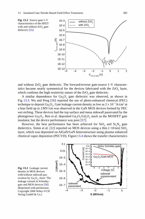
Gu et al. [55] reported on epitaxial growth of ZrO2 by oxides molecular beam epitaxy using reactive H2O2 for oxygen and metalorganic source for Zr. Utilizing a low temperature buffer layer followed by high temperature in situ annealing and high-temperature growth, monoclinic (100)-oriented ZrO2 thin films were obtained. The employment of epitaxial ZrO2 layer resulted in the increase of saturation-cur-rent density and pinch-off voltage as well as in near symmetrical gate-drain I–V behavior. Figure 13.2 compares the gate leakage current for the two devices—with
38513 Insulated Gate Nitride-Based Field Effect Transistors
and without ZrO2 gate dielectric. The forward/reverse gate-source I–V character-istics became nearly symmetrical for the devices fabricated with the ZrO2 layer, which confirms the high resistivity nature of the ZrO2 gate dielectric.
A similar dependence for Ga2O3 gate dielectric was observed, as shown in Fig. 13.3. Wu and Peng [56] reported the use of photo-enhanced chemical (PEC) technique to deposit Ga2O3. Gate leakage current density as low as 2 × 10⁻⁷ A/cm2 at a bias field up to 2 MV/cm was observed in the GaN MOS devices formed by PEC wet etching. These devices had the top surface and mesa sidewall passivated by the photogrown Ga2O3. Ren et al. deposited Ga2O3/Gd2O3 stack as the MOSFET gate insulator, but the device performance was poor [57].
However, the best performance has been achieved for SiO2 and Si3N4 gate dielectrics. Simin et al. [22] reported on MOS devices using a thin (~10 nm) SiO2 layer, which was deposited on AlGaN/GaN heterostructure using plasma enhanced chemical vapor deposition (PECVD). Figure 13.4 shows the transfer characteristics
Fig. 13.2 Source-gate I–V characteristics of the HFET with and without ZrO2 gate dielectric [55]
–4 –3 –2 –1 0 1 2VSource-gate (V)
I Sou
rce-
gate
(A)
–5
1E-3
1E-4
1E-5
1E-6
1E-7
1E-8
1E-9
1E-10
1E-11
1E-12
1E-13
without ZrO2
with ZrO2
Fig. 13.3 Leakage current density in MOS devices with/without sidewall pas-sivation by Ga2O3. Inset: The leakage current in Schottky-gate and MOS devices [56] (Reprinted with permission. Copyright 2006 Wiley-VCH Verlag GmbH & Co.)
–4 –3 –2 –1
–5 –4 –3 –2 –1 0
1E–91E–81E–71E–61E–5
1E–4
1E–30.01
0E (MV/cm)
sidewallpassivated
Ni/Au Schottky gate
Ga2O3 /GaN MOS
sidewallunpassivated
J (A
/cm
2 )
0.1
0.01
1E–3
1E–4
1E–5
1E–6
1E–7
Voltage (V)
Cur
rent
(A
)

386 M. Shur et al.
for the 1.5 µm gate MOSHFET and HFET measured at the drain voltage sufficient to shift the operating point into saturation regime. The figure also shows the gate bias dependence of the HFET and MOSHFET current in the saturation regime (for the MOSHFET the gate current remains in the low nA range). As seen, the gate volt-age corresponding to the maximum of IDS in the HFETs also corresponds to a sharp increase of the gate leakage current. This indicates that the mechanism responsible for the IDS saturation at high gate bias is the gate leakage current. In the MOSH-FETs, where the gate leakage is suppressed, the 2D electrons spillover into the AlGaN barrier becomes a limiting mechanism. A larger gate-channel separation in MOSHFET contributes to a higher value of gate voltage. Due to these factors, both the saturation gate voltage and the saturation current for the MOSHFETs are higher than those for the HFETs.
Simin et al. [22] also reported on insulated gate HFETs using Si3N4. Two sets of devices with identical geometry were fabricated on the same wafer. They consisted of MOSHFETs (10 nm SiO2 under the gate and in the source-gate and drain-gate regions) and MISHFETs (10 nm Si3N4 insulator replacing SiO2). Both the SiO2 and the Si3N4 layers were deposited using PECVD.
Figure 13.5 illustrates the transfer curves and the gate-leakage current curves for the MOSHFETs and MISHFETs. As seen, the maximum saturation currents in both MOSHFET and MISHFET are close. Either oxide or the nitride insulator layers reduce the gate leakage by 6–5 orders correspondingly below that measured for the typical HFET devices. The gate leakage current of the MISHFET is higher than of the MOSHFET, probably due to a lower quality of the thin Si3N4 layer. However, the increase in the threshold voltage for the MISHFET device is not as large. This follows directly from a higher value of the dielectric constant of the Si3N4 layer (εr = 3.9 for SiO2 and εr = 7.5 for Si3N4).
Wu et al. reported on MISFETs using atomic-layer-deposited (ALD) Al2O3 as the gate dielectric [58]. Compared to a GaN MESFET of similar design, the MOS-FET exhibited several orders of magnitude lower gate leakage and nearly three times higher channel current. Figure 13.6 illustrates the saturated ( Vds = 16 V) drain
Fig. 13.4 Maximum saturation and gate leakage currents in 1.5 µm gate MOSHFET with SiO2 and HFET devices [22] (Reprinted with permission. Copyright 2004 World Sci-entific Publishing Co.)

38713 Insulated Gate Nitride-Based Field Effect Transistors
current density and extrinsic transconductance gm as a function of gate bias for a GaN MOSFET and a MESFET of similar designs. The drain current density of the MESFET is limited to 70 mA/mm at Vgs = 1 V. The gate leakage current of the MESFET becomes unmanageable once the gate bias sweeps above 1 V due to low Ni/n-GaN Schottky barrier. By contrast, the drain current density of the MOSFET is 180 mA/mm at Vgs = 5 V and can be further increased under higher Vgs. The higher drain current achieved by employing Al2O3 gate oxide can be used to enhance the output power of the MOSFET compared to that of the MESFET.
More recently, very encouraging results were obtained for the structures employ-ing HfO2 as the gate dielectric. Figure 13.7 shows the transistor characteristic of AlGaN/GaN MOSHFET (referred to as MOS-HEMT by the authors) using reac-tive-sputtered HfO2 as the gate dielectric from ref. [59]. The dielectric constant of HfO2 found from the capacitance was estimated to be equal to 21. MOSHFETs
Fig. 13.5 Gate leakage current (a) and transfer characteristics (b) comparison for the MOSHFET and MISHFET fabricated on the same wafer. The inset shows the gate leakage current for a regular HFET [22] (Reprinted with permission. Copyright 2004 World Scientific Publishing Co.)
Gate voltage, V
1.501x10⁻⁸
1x10⁻¹⁰
1x10–12
1x10–14
1.25
1.00
0.75
0.50
0.00
0.25
–10 –5 0–14 –12 –10 –8 –6 –4 –2 0 2
Dra
in c
urre
nt, A
/mm
Gat
e cu
rren
t, A
MOSHFET
Vg, V-8 -4 -2 0 2
1E-12
1E-10
1E-9
1E-6
1E-4 Ia-Va FOR HFET
I Ca(
A/m
m)
MISHFET
MOSHFET
MIS
HFET
HFE
T
Gate voltage, VGa b
Fig. 13.6 The transfer and transconductance character-istics measured in the GaN MOSFET with Al2O3 and MESFET in saturation ( Vds = 16 V) [58] (Reprinted with permission. Copyright 2006 Elsevier)
25250
200
150
100
50
0–10 –8 –6 –4 –2 0 2 4
Vgs (V)
GaN MOSFET with 8 nm Al2O3
GaN MESFETLg = 1µmVds = 16v
I ds (
mA
/mm
)
g m (
mS
/mm
)
20
15
10
5
0

388 M. Shur et al.
exhibited a maximum drain current of 830 mA/mm and the gate leakage current at least five orders of magnitude lower than that of the reference HEMTs.
Tokranov et al. [36] reported on HfO2/AlGaN/GaN structures using HfO2 depos-ited by a reactive e-beam evaporation of Hf with oxygen. The structures were studied by means of impedance measurements. Figure 13.8 shows the results of the capacitance—voltage measurements (a) and DC leakage current of the studied structures (b). The dielectric constant of the HfO2 ε = 23, 24 was found to be close to the highest reported values for this material. The conductance measurements indi-cated a low concentration of the interface traps in comparison with the electron con-centration in the channel. These structures have been used to fabricate MISHFETs with HfO2/SiO2 gate dielectric stacks [60, 61].
Fig. 13.7 Typical output characteristics of AlGaN/GaN MOS-HEMT with 23 nm reactive sput-tered HfO2 as the gate dielectric [59] (Reprinted with permission. Copyright 2006 American In-stitute of Physics)
I DS (
mA
/mm
)
I DS (
mA
/mm
)
1000
800
600
400
200
00
a b2 4 6 8 10 12 14
VDS (V) VGS (V)
VGS = +6V to –6 V
Step = –1V
1000
800
600
400
200
0–8 –6 –4 –2 0 2 4 6
0
20
40
60
80
100
120
140
g m (
mS
/mm
)
MOS-HEMTConventional HEMT
Fig. 13.8 a Capacitance as a function of the gate voltage for the control (no HfO2), as-deposited, and annealed samples. The inset shows the contact configuration: D1 = 7.27 × 10⁻² cm, D2 = 0.153 cm. b DC leakage current measured at different locations on the wafer with annealed HFO2 [36] (Reprinted with permission. Copyright 2007 Wiley-VCH Verlag GmbH & Co.)
6x10⁻⁷
5x10⁻⁷
4x10⁻⁷
3x10⁻⁷
2x10⁻⁷
1x10⁻⁷
0–10 –5 0 5 10 15
C, F
/cm
2
Hg
controlHfO2 annealed650C, 30sas deposited HfO2
V, Va b
I A/c
m2
10–2
10–3
10–4
10–5
10–6
10–7
10–8
10–9
10–10
–15 –10 –5 0 5 10V, V

38913 Insulated Gate Nitride-Based Field Effect Transistors
13.3 Transport Properties
First Monte Carlo calculations for GaN were done by Littlejohn et al. in 1975 [62]. Later, the Monte Carlo simulations have been used to simulate the electron transport within GaN [63–70], AlN [69, 71, 72] and InN [6, 7, 69, 73–76]. The Monte Carlo simulation approach has also been used to analyze the electron transport within the 2DEG at the AlGaN/GaN interface [6, 7, 77, 78]. Figure 13.9 compares computed velocity-field characteristics of nitride materials [69]. As seen, InN and GaN are faster materials than GaAs and, in transient regime they can be even faster (see Fig. 13.10).
Fig. 13.9 Monte-Carlo simulation of the drift veloc-ity versus electric field for several III-V compounds (InN is the fastest nitride material) [69] (Reprinted with permission. Copyright 1999 American Institute of Physics)
Drif
t Vel
ocity
[cm
/s]
108
107
106
101 100 1000Electric Field [kV/cm]
65 kV/cm
4 kV/cm
GaAs
InN
140 kV/cm
GaN
450 kV/cmAlN
Fig. 13.10 Average electron velocity as a function of the displacement for different electric fields for InN [69] (Reprinted with permission. Copyright 1999 American Institute of Physics)
Drif
t Vel
ocity
[107
cm/s
]
10
8
6
4
2
00.0 0.2 0.4 0.6 0.8
Distance [µm]
260 kV/cm
130 kV/cm
97.5 kV/cm65 kV/cm
32.5 kV/cm
InN
390 M. Shur et al.
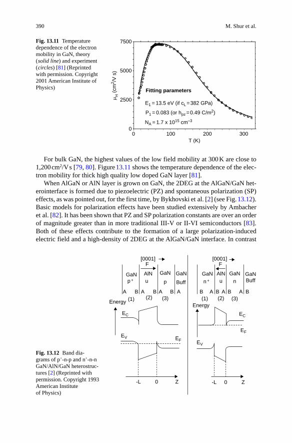
For bulk GaN, the highest values of the low field mobility at 300 K are close to 1,200 cm2/V s [79, 80]. Figure 13.11 shows the temperature dependence of the elec-tron mobility for thick high quality low doped GaN layer [81].
When AlGaN or AlN layer is grown on GaN, the 2DEG at the AlGaN/GaN het-erointerface is formed due to piezoelectric (PZ) and spontaneous polarization (SP) effects, as was pointed out, for the first time, by Bykhovski et al. [2] (see Fig. 13.12). Basic models for polarization effects have been studied extensively by Ambacher et al. [82]. It has been shown that PZ and SP polarization constants are over an order of magnitude greater than in more traditional III-V or II-VI semiconductors [83]. Both of these effects contribute to the formation of a large polarization-induced electric field and a high-density of 2DEG at the AlGaN/GaN interface. In contrast
Fig. 13.11 Temperature dependence of the electron mobility in GaN, theory ( solid line) and experiment ( circles) [81] (Reprinted with permission. Copyright 2001 American Institute of Physics)
µ H (
cm2 /
V s
)
7500
5000
2500
00 100 200 300
T (K)
Fitting parameters
E1 = 13.5 eV (if cL = 382 GPa)
P1 = 0.083 (or hpz = 0.49 C/m2)
NA = 1.7 x 1015 cm–3
Fig. 13.12 Band dia-grams of p+-n-p and n+-n-n GaN/AlN/GaN heterostruc-tures [2] (Reprinted with permission. Copyright 1993 American Institute of Physics)
[0001] [0001]F F
GaN GaN GaN GaN GaN GaNAlN AlNp + u up n + nBuff Buff
A A A A A A AB B B B B B B(1) (1)(2) (2)(3) (3)
EnergyEnergy
EC EC
EVEV
EF
EF
-L -L0 0Z Z

39113 Insulated Gate Nitride-Based Field Effect Transistors
to traditional HFETs, barrier doping for III-nitrides is not necessary to obtain high sheet charge density [84].
Due to the existence of polarization in III-nitride heterostructures, the 2DEG elec-tron concentration and subsequent device performance depend on a number of physi-cal properties including polarity, strain, thickness, and barrier doping. The strain in the AlGaN layer is related to its thickness and composition. Aluminum composition in the range of 20–30% results in a large band offset and has a reasonably high critical thickness allowing for pseudomorphic growth up to 50–100 nm. 20–30% Al content gives a good compromise between mobility and sheet charge. Higher Al content provides better carrier confinement and increased sheet charge, but increased alloy scattering degrades mobility. At lower Al content, mobility remains roughly the same, but the reduced carrier confinement results in low sheet carrier concentration.
For pseudomorphic AlGaN on GaN, the strain is tensile and both the PZ and SP are directed opposite to the growth direction if the material is Ga-face and along the growth direction if the material is N-face [82]. MOCVD growth resulting in smooth surface morphology is always Ga-face polarity. Thus, the polarization will induce a positive charge in the AlGaN. A positive fixed polarization charge in the AlGaN layer is compensated by free electrons in the channel region. Free electrons are pro-vided by the unintentional doping of the heterostructure or through surface donors states of AlGaN [84]. Due to the surface donor states, the 2DEG density increases and then saturates with increasing AlGaN thickness.
As the electrons are confined in a Two-Dimensional (2D) quantum well, bulk scattering effects such as ionized impurity scattering are eliminated, resulting in much higher mobility than for bulk GaN. As the quantum well is formed at the AlGaN/GaN interface, the main factors influencing 2DEG mobility are interface, alloy and dislocation scattering. Modified AlGaN/AlN/GaN structures, which employ a thin AlN interfacial layer between AlGaN and GaN layers, show higher 2DEG properties than those of conventional AlGaN/GaN structures [85]. This high performance is achieved due to the increased ΔEC, which effectively suppresses the electron penetration from the GaN channel into the AlGaN layer, and results in the reduction of alloy disorder scattering.
Figure 13.13 shows the polarization directions in AlGaN/GaN layers grown on Ga and N substrates [82] and Fig. 13.14 presents calculated 2DEG densities [86]. Figure 13.14 shows the computed values of the 2DEG concentration at the AlGaN/GaN heterointerface as a function of the Al molar fraction for different thicknesses of the AlGaN wide band gap barrier layer. The dashed lines do not account for the stress relaxation at the critical thickness, when strain leads to the development of the dislocation arrays. As seen, the 2DEG densities on the order of 3 × 1012 cm−2 can be reached. Even higher sheet carrier densities can be obtained using nearly lattice-matched AlInN/GaN heterostructures [87]. Figure 13.15 shows the computed 2DEG sheet density induced in AlInN/AlN/GaN heterostructures (without any additional doping).
Low field mobility in 2D channel on the GaN/AlGaN interface is quite high, exceeding for 2D electrons 2,000 cm2/V s at 300 K [4, 88], see Fig. 13.16.

392 M. Shur et al.
Fig. 13.13 Polarization directions in AlGaN/GaN layers grown on Ga and N substrates [82] (Reprinted with permission. Copyright 1999 American Institute of Physics)
Psp Psp
Psp
Psp
Psp
Psp
Psp
Psp
Psp
Psp
Ga face
AlGaN AlGaN
AlGaN
AlGaN
AlGaN
AlGaN
GaN GaN
GaN
GaN
GaN
GaN
[0001] [0001]
+
+
-
-
-
+
Ppe
Ppe
Ppe
Ppe
N face
Relaxed
Relaxed
Relaxed
Relaxed
TensileStrain
CompressiveStrain
Fig. 13.14 Computed values of the 2DEG concentration at the AlGaN/GaN heter-ointerface as a function of Al molar fraction for different thicknesses of AlGaN barrier layer [86] (Reprinted with permission. Copyright 2000 Elsevier)
Sh
eet
den
sity
(10
13 c
m–2
)
6
5
4
3
2
1
00 0.2 0.4 0.6 0.8 1
Al Molar Fraction
30 n
m
10 n
m
5 nm

39313 Insulated Gate Nitride-Based Field Effect Transistors
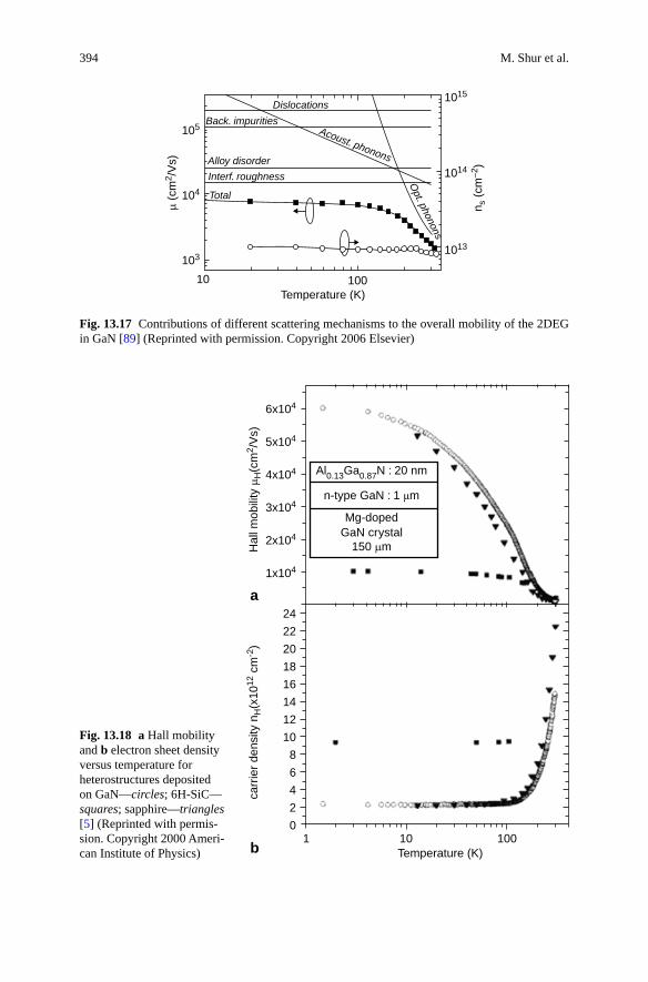
The drop in mobility with increasing the 2D density is an indication of the elec-tron transfer into AlGaN that occurs because the Fermi level at the heterointerface is pushed too high and, at high densities, electrons cannot be fully contained in the quantum well formed at the heterointerface. Figure 13.17 shows the relative contri-butions of different scattering mechanisms to the overall mobility of the 2DEG in GaN [89].
Figure 13.18 compares temperature dependences of the 2DEG mobility in GaN grown on different substrates [5]. In field effect transistors, the electron mobility depends on the gate bias, which controls the 2DEG density in the channel.
Fig. 13.15 Computed 2DEG sheet density in AlInN/AlN/GaN heterostructures
She
et e
lect
ron
conc
entr
atio
n (m
–2 ) 6.5 x 10
17
6.0 x 10¹⁷
5.5 x 10¹⁷
5.0 x 10¹⁷
4.5 x 10¹⁷
0.2 0.4 0.6 0.8 1.0
Fraction of Al in AlInGaN
Fig. 13.16 Electron Hall mobility in Al0.2Ga0.8N/GaN heterostructures with different levels of GaN channel doping measured at room temperature (a) and T = 77 K (b). Solid dots correspond to heterostructures grown on sapphire, open circles—on conducting 6H-SiC, triangles—on insulat-ing 4H-SiC [88] (Reprinted with permission. Copyright 1999 American Institute of Physics)
Hal
l Mob
ility
(cm
2 /V
-s)
Hal
l Mob
ility
(cm
2 /V
-s)
2,100
1,800
1,500
1,200
900
600
0 1 2 3 4
2D Electron Density (x1013 cm–2)a b 2D Electron Density (x1013 cm–2)
Al0.2Ga0.8N-GaN
10,000
8,000
6,000
4,000
2,000
00.0 0.5 1.0 1.5 2.0 2.5 3.0 3.5
T = 77 K
394 M. Shur et al.
Fig. 13.17 Contributions of different scattering mechanisms to the overall mobility of the 2DEG in GaN [89] (Reprinted with permission. Copyright 2006 Elsevier)
µ (c
m2 /
Vs)
105
104
103
10 100Temperature (K)
Dislocations
Back. impurities
Alloy disorder
Interf. roughness
Total
Acoust. phonons
Opt. phonons
1015
1014
1013
n s (
cm–2
)
Fig. 13.18 a Hall mobility and b electron sheet density versus temperature for heterostructures deposited on GaN—circles; 6H-SiC—squares; sapphire—triangles [5] (Reprinted with permis-sion. Copyright 2000 Ameri-can Institute of Physics)
Al0.13Ga0.87N : 20 nm
n-type GaN : 1 μm
Mg-dopedGaN crystal
150 µm
6x10⁴
5x10⁴
4x10⁴
3x10⁴
2x10⁴
1x10⁴
Hal
l mob
ility
µH(c
m2 /
Vs)
carr
ier
dens
ity n
H(x
1012
cm
-2)
24
22
20
18
16
14
12
10
8
6
4
2
01 10 100
Temperature (K)
a
b

39513 Insulated Gate Nitride-Based Field Effect Transistors
Ivanov et al. extracted effective mobility in the channel of GaN/AlGaN MOSHFET with 10 nm thick SiO2 gate dielectric from the transfer current voltage characteristics [90]. Figure 13.19 shows the electron mobility as a function of the 2D concentration (changed by the gate voltage). As seen, the mobility is of the same order of magnitude as for regular HFETs, indicating that gate dielectric does not degrade the mobility. The inset shows the dependence of the channel conductivity Gch versus gate voltage VG.
13.4 Device Design and Fabrication
Typical GaN MOSFET and MOSHFET designs are illustrated in Figs. 13.20 and 13.21.
The gate oxide for MOSFETs and MOSHFETs is formed by deposition of SiO2 [18, 32, 91], Ga2O3/Gd2O3 stack [57], Si3N4 [92, 93], Al2O3 [94], Sc2O3 [95], ZrO2 [96], AlN [97, 98] and others.
Fig. 13.19 The electron mobility dependence on sheet concentration of 2DEG in the channel of MOSHFET [90]
Mob
ility
(cm
2 / V
s)
1600
1200
800
400
00.0 0.2 0.4 0.6 0.8 1.0 1.2
ns / 1013 (cm–2)
VG (V)–6 –4 –2 0 2
Gch
(m
A/V
)
8
6
4
2
0
Fig. 13.20 Schematic cross section of a lateral n-channel GaN MOSFET [32] (Reprinted with permission. Copyright 2006 IEEE)
SourceGate Oxide
n+ Poly-Si Drain
n+ n+p or n-GaN
Sapphire Substrate

396 M. Shur et al.
MOSFETs can be fabricated on p or n-GaN epilayers. To form the highly doped contact regions, source and drain areas are selectively implanted with Si atoms. GaN MOSFET operation is similar to that for Si-based devices. At zero gate bias, the source-drain region has very high resistance due to high resistivity of GaN (for an n-GaN buffer) or the presence of two back-to-back connected p-n junctions (for a p-GaN buffer). A conducting channel in MOSFETS is formed by applying gate bias inducing relatively high electron (n-channel) or hole (p-channel) concentration.
In MOSHFETs, as in regular AlGaN/GaN HFETs, the built-in channel is formed by the high-density 2D electron gas at the AlGaN/GaN interface. However, in con-trast to a regular HFET, the gate metal is isolated from AlGaN barrier layer by a thin dielectric film (see Fig. 13.21). Thus, the MOSHFET gate behaves more like a MOS gate structure rather than a Schottky barrier gate used in regular HFETs. Since the properly designed AlGaN barrier layer is fully depleted, the gate insula-tor in the MOSHFET consists of two sequential layers: the dielectric film and the AlGaN epilayer. This double layer ensures an extremely low gate leakage current and allows for a large negative to positive gate voltage swing.
Typical MOSHFET fabrication process is close to that of regular Schottky gate HFETs. The ease of MOSHFET fabrication and compatibility with the HFET processing is another big advantage of the MOSHFET technology. Device fabrica-tion normally starts with mesa isolation done using Reactive Ion Etching (RIE) or ion implantation to define the active area. Ohmic contacts are then being formed, most often using Ti/Al/Ti/Au stacks, although a number of more advance contact schemes have been reported to achieve lower contact resistance [99]. The next step is the gate dielectric formation. Typically, plasma-enhanced chemical vapor depo-sition (PECVD) is used to deposit films like SiO2 or Si3N4. Other materials, like HFO2 have been successfully deposited using ALD or e-beam techniques [36]. The dielectric deposition technique as well as the pre-deposition surface preparation, temperature regime etc. have crucial effect on the quality of the deposited films, the MOSHFET threshold voltage, dispersion effects and device reliability.
A lift-off process is typically used for MOSHFET fabrication. Prior to dielectric film deposition the wafer is covered with photoresist and a photolithography is used to pattern the wafer to remove the photoresist in the source—drain spacing. After the dielectric film deposition, the lift-off operation removes the dielectric outside the source-drain region. The remaining processing steps are no different from the HFET fabrication: metal gate deposition, normally Ni/Au, followed by optional passivation, field-plating, contact pad formation and electroplating.
Fig. 13.21 Typical MOSHFET design. The substrate material could be SiC, sapphire, bulk GaN, bulk AlN, or Si
S G Dielectric D
AlGaN
GaN
Substrate

39713 Insulated Gate Nitride-Based Field Effect Transistors
Packaging for AlGaN/GaN power MOS and MOSHEFT devices is often similar to that used for silicon or III-V power devices. However, packaging for GaN-based devices is more challenging because of their higher power. Flip-chip mounting of the die is a preferred solution (see Fig. 13.22).
13.5 Device Characteristics
13.5.1 Current-Voltage Characteristics and Threshold Voltage
GaN MOSFETs are mostly normally-off (enhancement mode) devices [101]. Typi-cal set of MOSFET drain current-voltage characteristics is shown in Fig. 13.23.
Fig. 13.22 Two flip-chip designs: First design has metal bumps placed on the source, drain and gate contact pad. The second design has additional bumps placed directly on the source and drain ohmic contacts to provide direct thermal and electrical contact between the ohmic contacts and the metal pads on the AlN carrier [100] (Reprinted with permission. Copyright 2006 IEEE)
Source, drain& gate contacts
SapphireSapphire
AlGaN/GaNAlGaN/GaN
AlN AlN
Flip-chip bumps
Fig. 13.23 Drain I–V char-acteristics of MOSFET on n-GaN [32] (Reprinted with permission. Copyright 2006 IEEE)
Dra
in C
urre
nt (
mA
/mm
)
30
25
20
15
10
5
00 5 10 15 20 25
Drain Voltage (V)
VG = 20V
VG = 16V
VG = 12V
VG = 8V
VG = 0-4V
398 M. Shur et al.
The threshold voltage varies from 0 to +5 V depending on the GaN buffer layer doping and dielectric type and thickness. General MOSFET expressions for transconductance, capacitances and other characteristics are as well applicable to GaN MOSFETs.
MOSHFET I–V characteristics are similar to those of Schottky-gate HFETs. However, the threshold voltage is different and depends on the dielectric layer thickness and permittivity. Due to a larger gate-to-channel separation, the threshold voltage of the MOSHFET is more negative than that of an HFET. Assuming the same sheet charge density in the channel for MOSHFET and HFET devices at zero gate bias and ignoring the surface charge QS at the dielectric/AlGaN interface, the threshold voltages for the MOSHFET and HFET can be related as:
(13.1)
Or
(13.2)
Here CMOSH and CMS are the capacitances of equal area pads on the oxide and non-oxide areas and εOX is the dielectric permittivity of the gate dielectric; dOX and db are the thicknesses of dielectric and barrier layers correspondingly, VTMOS and VTMS are correspondingly the absolute values of the MOSHFET and HFET threshold voltages.
The oxide thickness dOX can be extracted from the measured gate capacitances:
(13.3)
The DC saturation drain current, IDS, is a key parameter controlling the maximum output RF-power. This current IDS increases with positive gate voltages until it reaches its maximum value, IDMAX. However, for conventional AlGaN/GaN GaN HFET’s, gate voltages in excess of +1.2 V result in an excessive leakage cur-rent, which limits IDS, decreases the transconductance and increases the noise. In MOSHFETs, gate voltages as high as +10 V could be applied. This results in about 100% increase in the IDS value with respect to the zero gate bias value. The gate leakage, however, remains well below 1 nA/mm [102]. Figure 13.24 shows the transfer characteristics for different gate length HFETs (a) and MOSHFETs (b) measured at the drain voltage sufficient to shift the operating point into saturation regime. Figure 13.24a also shows the gate bias dependence of the gate current in the saturation regime (the gate currents for MOSHFETs are very low and not shown). Maximum drain currents in HFETs are limited by the forward gate currents that are triggered at internal gate voltage exceeding approximately VGM ≈ 1.7 V [102]. In the MOSHFETs, where the gate leakage is suppressed, the 2D electrons spillover into
QS = qNS = CMOSH × VTMOS = CMS × VTMSQS = qNS = CMOSH × VTMOS = CMS × VTMS
VT MOS = VTMSCMS/CMOSH = VTMS ×
1 +dOX
dB·
εB
εOX
.VT MOS = VTMSCMS/CMOSH = VTMS ×
1 +
dOX
dB·
εB
εOX
.
CMOS =ε0εB
dB×
1+dOX
dB·
εB
εOX
−1
= CMS ×
1+dOX
dB·
εB
εOX
−1
CMOS =ε0εB
dB×
1+dOX
dB·
εB
εOX
−1
= CMS ×
1+dOX
dB·
εB
εOX
−1

39913 Insulated Gate Nitride-Based Field Effect Transistors
the AlGaN barrier becomes a limiting mechanism. For SiO2 based MOSHFETs, the corresponding maximum internal gate voltage was found to be around VGM ≈ 5 V [102].
The MOSHFET saturation currents IDS0 for the zero gate bias are in a good agree-ment with the analytical model proposed in [103]:
(13.4)
Whereas maximum achievable drain currents IDM can be found as:
(13.5)
In these expressions, VT is the threshold voltage, VGMT = VGM − VT, Rs is the source-gate series resistance, β = Ciµ
LG, VL = vsLG
µ, where Ci is gate-channel capacitance per
unit area, µ is the electron field effect mobility, vs is the effective electron saturation velocity. Assuming that the maximum sheet carrier density in the 2DEG channel, ns, is about 2 × 1013 cm−2 [86] and the effective electron drift velocity in the chan-nel, v = 5 × 106 cm/s, we estimate the maximum achievable channel current IDM/W = q × ns × v ≈ 1.6 A/mm. The measured saturation current in MOSHFETs (Fig. 13.24b) is close to this maximum value.
The internal drain voltage for the drain current saturation (the knee voltage VKN) for MOSHFETs is of the same order as that for HFETs for same drain currents [22].
IDS0 = β ·V 2
T
1 + β · Rs · VT +
1 + 2β · Rs · VT + V 2T
V 2L
IDS0 = β ·V 2
T
1 + β · Rs · VT +
1 + 2β · Rs · VT + V 2T
V 2L
IDM = β ·V 2
GMT
1 +
1 + VGMT/V 2L
IDM = β ·V 2
GMT
1 +
1 + VGMT/V 2L
Fig. 13.24 Gate bias dependencies of the drain saturation current and gate leakage current for HFET (a) and MOSHFET (b) devices. For MOSHFETs gate leakage current is negligibly small and not shown. Drain bias corresponds to the saturation region of the device I–V characteristics. Gate length is given in micron next to the curves [102] (Reprinted with permission. Copyright 2002 American Institute of Physics)
I DS
, A/m
m
a b
I DS, A
/mm
1.2
1.0
0.8
0.6
0.4
0.2
0.0
IDS
11
IG
20
20
40
40
60
60
80
80
–2 0 2 4 6 8VG, VVg, V
0.12
0.10
0.08
0.06
0.04
0.02
0.00
I G, A
/mm
1.8
1.6
1.4
1.2
1.0
0.8
0.6
0.4
0.2
0.0
1
10 2040 60
80
–4 –2 0 2 4 6 8 10 12 14 16 18

400 M. Shur et al.
However, since the MOSHFET drain currents are higher than those for HFETs, the MOSHFET current voltage characteristics have higher VKN values due to larger voltage drop across the source and drain access resistances. Since the threshold voltage of MOSHFET is more negative compared to HFETs, the MOSHFET DC transconductance is lower. However the small-signal gain and the cut-off frequen-cies for MOSHFETs are same or even higher than those of HFET. [22], since the MOSHFET gate—channel capacitance is also lower compared to HFET thus com-pensating the decrease in the transconductance.
The mechanism of the gate leakage in GaN-based MOSFETs is fairly com-plicated and involves surface leakage and trap-assisted tunneling [104, 105], see Fig. 13.25.
Simin et al. [106] reported on the characteristics of AlGaN/GaN MOSHFETs were measured in the temperature range of 20–300 °C. At 300 °C, the leakage cur-rent of MOSHFET remained four orders of magnitude lower than that of regular HFET. The saturation current and transconductance for both types of transistors follow the temperature dependence of electron velocity in the channel.
The recovery of the current collapse (see Sect. 13.6) at elevated temperatures compensated the effect of the decrease of the steady-state saturation current with temperature. As a consequence, the saturation microwave power remained nearly constant in the temperature range 20–200 °C, varying only by about 20% or so. These results showed high potential of MOSHFETs for high-temperature micro-wave, digital and switching applications. This was further confirmed by Tarakji et al. [107], who studied DC and RF-characteristics of AlGaN/GaN MOSHFETs at elevated temperatures up to 300 °C, after a 36 h continuous operation at 200 °C and after a 1 min thermal stress at temperatures up to 850 °C. At 300 °C, the gate leakage current remained about 4 orders of magnitude lower than that for regular HFETs. At zero gate-bias, the saturation current decreased by only about 20% after 36 h of con-tinuous operation at 200 °C. After a 700 °C, 1 min thermal stress, the gate leakage remained as low as 5 nA/mm, whereas the peak current and DC transconductance showed a 20% reduction. In spite of the decrease in the peak-current, the RF satura-
Fig. 13.25 Leakage current pass in AlGan/GaN MOSHFETs [104] (Reprinted with permission. Copyright 2002 Materials Research Society)
SiO2 leakageGate
Surface Leakage
Source Drain
AlGaN leakage

40113 Insulated Gate Nitride-Based Field Effect Transistors
tion power remained nearly constant for operation at temperatures up to 200 °C that they also attributed to a reduction in the current collapse.
Simin et al. [108] used the oxide layer in MOSHFETs for bridging to increase the device periphery. They reported on AlGaN/GaN MOSHFETs over SiC sub-strates with peripheries from 0.15 to 6 mm. The devices featured a multigate (MG) design with source interconnections using a novel oxide-bridging approach. The saturation current scaled linearly with the gate width and reached 5.1 A for a 6 mm wide device with a 1.5 µm gate length in a 5 µm source—drain opening. The cutoff frequency of around 8 GHz was practically independent of periphery. Large-signal output RF-power as high as 2.7 W/mm was measured at 2 GHz. The RF-power also scaled linearly with device widths up to 2 mm.
13.5.2 Low Frequency Noise
The level of the low frequency (1/f and generation–recombination) noise is one of the most important parameters of semiconductor devices. In microwave and optical devices (generators, mixers, lasers) it up-converts to the phase noise and sets a lower limit on the signal level in broad-band circuits, Doppler locators, communication systems. The noise limits also the sensitivity of any detector and determines the signal to noise ratio. Therefore, noise is one of the crucial factors which determine the possibility of practical use of the device, especially in com-munication systems.
The low frequency noise is also a powerful tool to study deep levels, degra-dation, material structural perfection, mechanisms of current flow, recombination, light emission etc. The presence of generation–recombination noise indicates the well-defined local level. Measurements as a function of temperature of this noise allow us to find energy position, concentration and capture cross section of this level. In some cases, the temperature dependence of the capture cross section can also be determined. This is so-called Noise Spectroscopy [109, 110]. Refer to Refs. [111–113] regarding the generation–recombination noise in GaN-based devices.
The review of the noise properties of nitrides and GaN-based devices can be found in references [114–116]. There are several known noise sources in FETs, including the gate leakage current. As was shown by Rumyantsev et al. [117], the gate leakage current might significantly contribute to noise for low noise devices even for the relatively small gate currents (on the order of 0.01% of the drain current or so). Since FETs transistors with insulated gate have several orders of magnitude smaller gate leakage current, they are free of the noise source related to the gate current. On the other hand, traps in the gate dielectric and at the dielectric-semi-conductor interface might cause additional noise. This noise mechanism known as McWhorter noise is the main noise source in Si MOSFETs [118, 119]. High-k die-lectrics (used for the reduction of gate leakage current in submicron Si MOSFETs) cause elevated noise levels in those devices [120, 121].

402 M. Shur et al.
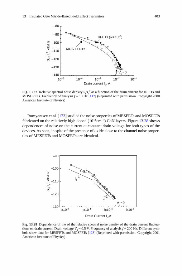
The noise properties of GaN-based HFETs with the SiO2 insulated gate (MOSH-FETs) were studied by Pala et al. [20] and Chiou et al. [122]. Pala et al. [20] fabricated the transistors with insulated and Schottky barrier gates on the same wafer. The SiO2 layer was deposited on a part of the heterostructure using plasma enhanced chemical vapor deposition. Figure 13.26 shows the transfer current voltage characteristics of the HFETs and MOSHFETs. As seen, MOSHFETs are character-ized by the extremely low gate current and high on-to-off ratio. Figure 13.27 shows the drain current noise SI/Id
2 as a function of the drain current at constant gate volt-age for both type of transistors. As seen, MOSHFET are characterized by the same or smaller noise level as HFETs, i.e., silicon dioxide does not deteriorate the noise characteristics of MOSHFETs.
Fig. 13.26 Transfer cur-rent–voltage characteristics of HFETs and MOSHFETs [117] (Reprinted with permission. Copyright 2000 American Institute of Physics)
Dra
in a
nd G
ate
Cur
rent
s I d
, Ig,
AD
rain
and
Gat
e C
urre
nts
I d, I
g, A
1x10⁻¹
1x10⁻¹
1x10⁻²
1x10⁻³
1x10⁻³
1x10⁻⁴
1x10⁻⁵
1x10⁻⁵
1x10⁻⁶
Gate voltage Vg, V–6 –5 –4 –3 –2 –1 0
Id
Id
Vd = (3–5) V Vd = 2V
Vd = 1V
HFET
Vd = 5V
Vd = 1VIg
1x10⁻⁷
1x10⁻⁹
1x10–11
–12 –10 –8 –6 –4 –2 0
Gate voltage Vg, V
Vd = (3–7) V
Vd = 1V
MOS-HFET
IgVd = 7V
Vd = 1V
40313 Insulated Gate Nitride-Based Field Effect Transistors
Rumyantsev et al. [123] studied the noise properties of MESFETs and MOSFETs fabricated on the relatively high doped (1018 cm−3) GaN layers. Figure 13.28 shows dependences of noise on the current at constant drain voltage for both types of the devices. As seen, in spite of the presence of oxide close to the channel noise proper-ties of MESFETs and MOSFETs are identical.
Fig. 13.27 Relative spectral noise density SI/Id2 as a function of the drain current for HFETs and
MOSHFETs. Frequency of analysis f = 10 Hz [117] (Reprinted with permission. Copyright 2000 American Institute of Physics)
SId
/ Id2 ,
dB
/Hz
–80
–90
–100
–110
–120
–130
–140
MOS-HFETs
HFETs ( =10–3)
10–5 10–4 10–3 10–2 10–1
Vg=0
Drain current Id, A
Fig. 13.28 Dependence of the of the relative spectral noise density of the drain current fluctua-tions on drain current. Drain voltage Vd = 0.5 V. Frequency of analysis f = 200 Hz. Different sym-bols show data for MESFETs and MOSFETs [123] (Reprinted with permission. Copyright 2001 American Institute of Physics)
–90
–100
–110
–120
–130lx10–5 lx10–3lx10–4 lx10–2
Drain Current Id,A
SId/ I
d2 , d
B/H
Z
Id
Id
–1
–2
Vg = 0

404 M. Shur et al.
13.6 Non-Ideal Effects and Reliability
Since the first report of the current collapse in AlGaN/GaN HFETs [97], which iden-tified the mechanism of this effect as related to hot electron trapping, the current collapse has been one of the hot topics of the AlGaN/GaN research and develop-ment. Due to the lack of native substrates, high growth temperatures and signifi-cant piezo-effects, the defect concentration in III-nitride heterostructures is several orders of magnitude higher than that in Si or GaAs based materials. Due to this, the trapping may occur in different device regions: buffer layer, barrier layer and at the surface. In MOSHFETs, additional trapping may take place at the dielectric-bar-rier interface. Common feature of the current collapse in nearly all the III-nitride devices is the gate edge-related nature of this effect. Simin et al. [124] presented experimental evidence of the gate edges being responsible for the current collapse, as illustrated in Fig. 13.29.
As seen, during the transient, the portion of the resistance corresponding to the channel under the gate does not change (R(0) and R(τ) have the same slope); the difference comes from the gate length-independent shift which can be attributed to the time-dependent resistance at the gate edge. Similar behavior was found for GaN MESFETs and MOSFETs in [125]. Numerous factors may be responsible for the carrier trapping at the gate edges. These include strong electric fields at the drain edge of the gate, surface states [126], buffer trapping [127] and voltage induced strain in the layers forming the heterostructure [124].
Apart from the obvious way of reducing the dislocation density and defect con-centration in the III-nitride heterostructures, an effective approach to reducing or eliminating the current collapse was found by surface passivation, typically using the Si3N4 layers [128]. Other materials have also been shown to provide the passi-
Fig. 13.29 a test pattern and b gate length dependence of the initial and steady state channel re-sistance. The test pattern consists of a set of transistors with constant source-gate and gate-drain spacing and variable gate length LG. The channel resistance was measured in the beginning of the pulse applied to the drain: R(0) and after reaching a steady state condition: R(τ) [124] (Reprinted with permission. Copyright 2001 American Institute of Physics)
LG
R, k
2.5
2.0
1.5
1.0
0.5
0.00
a b
20 40 60 80 100 120 140LG, m
R(0)R( )
R
R, k
1.0
0.8
0.6
0.4
0.2
0.0

40513 Insulated Gate Nitride-Based Field Effect Transistors
vation effects and to eliminating or reducing the current collapse, such as SiO2 and silicon-oxynitride layers [129], or HfO2 layers [59]. The mechanism of surface pas-sivation is related to several factors. One of them is the surface field reduction due to high dielectric constant of the deposited dielectric film (see Fig. 13.30).
The ability of the dielectric layer to mitigate the current collapse also depends on many other factors, such as polarization and built-in charges, lattice matching to the barrier layer material, conductivity, structural quality etc. Because of this complex-ity, surface passivation effects are still poorly reproducible. The above considera-tions are fully applied to the gate dielectric materials used in MOSFET/MOSHFET technology, which may or may not provide the passivation effects.
Another efficient approach to mitigating the current collapse is by implementing a so-called field-plating technology [131]. Field-modulating plate smoothens out strong electric field peak at the gate edge and thus increases the drain voltage needed to reach the threshold for hot electron trapping. This effect is illustrated in Fig. 13.31 [132].
The reliability and degradation processes in power GaN HFETs and MOSH-FETs have been found to be strongly related to the carrier trapping and hence to the current collapse effects [132–134]. It has been shown that eliminating the current collapse using the above reviewed approaches allows for greatly increased lifetime of GaN based devices. The reliability of insulating gate devices is typically much better than those with Schottky based gates. The mechanism of enhanced MOSH-FET reliability is related to low MOSHFET gate currents under dynamic forward gate biasing that is present in high power switches or microwave power amplifiers. In HFETs, such forward bias causes significant gate currents resulting in fast degra-dation. In MOSHFETs, the gate currents remain at low level allow for stable high-power operation [133, 135, 136]. Fujitsu Inc. has demonstrated and insulating gate AlGaN/GaN HFET with over 100 W output power and estimated lifetime exceeding one million hours [137].
Fig. 13.30 Reduction in the surface peak field at the gate edge due to dielectric layer with high dielectric permittivity [130] (Reprinted with permission. Copyright 2006 IEEE)
ε = 7.5
ε = 1
–0.1
0.0
0.1
0.20 0.2
0 0.2 0.4
0 1000 2000 3000 4000 5000 6000 7000 8000

406 M. Shur et al.
13.7 Applications and Performance
13.7.1 RF Amplifiers
RF power amplifier is the most important and widely used application of GaN based field-effect transistors [138]. Due to extremely high drain saturation currents and breakdown voltages, in combination with high operating temperatures, chemical stability and robustness, GaN power amplifiers have outperformed most other solid state amplifier types. Using GaN based amplifiers, for the first time the RF power densities as high as 30 W/mm (Watt per 1 mm of the device periphery) have been achieved [139, 140]. These power densities are one–two orders of magnitude higher than those obtained with Si, SiC or III-V semiconductor devices.
The use of insulated gate GaN devices in power amplifiers play crucial role in achieving simultaneously the highest power densities and high stability and reli-ability. HFET operation as an RF power amplifier is illustrated in Fig. 13.32. In a typical circuit configuration, the voltage applied at the gate is a superposition of the DC bias and the input RF signal (Fig. 13.32a). Changes in the HFET drain current
Fig. 13.31 The field dis-tribution along the 2-DEG under optimum conditions for large plate extension l. a Model, b Comparison between model ( line) and numerical calculations ( points) of the x-component of the field [132] (Reprinted with permission. Copyright 2005 IEEE)
Fie
ld a
long
the
2-D
EG
0
l
x
a
b
Distance from source (µm)
Exponentialdecay
Ele
ctric
Fie
ld (
MV
/cm
)
0.8
–0.2
0.0
–0.4
–0.6
–0.8
1.0 1.2 1.4 1.6
Wδ W

40713 Insulated Gate Nitride-Based Field Effect Transistors
caused by the gate voltage modulation, result in the modulated voltage across the load resistance RL. The maximum linear output RF power can be estimated using the following simple approximate expressions. For linear mode amplification (so-called Class A mode), the DC bias corresponds to approximately half the maximum HFET drain current IDMAX; as seen from the Fig. 13.32b, corresponding maximum amplitude of the RF current, iMAX = IDMAX/2. Peak drain voltage may not exceed the breakdown voltage VBD; therefore, maximum amplitude of the output RF signal is vMAX = VBD/2 − VKN, where VKN is the drain voltage for the drain current saturation. Since typically, VKN << VBD, the maximum HFET output power, PMAX = iMAX × vMAX/2 ≈ IDMAX × VBD/8. In typical modern microwave HFETs, peak drain currents can be as high as IDMAX = 1.5–2 A/mm, with breakdown voltages VBD ≈ 100–150 V. Hence maximum RF powers can be as high as 18–37 W/mm. The above example explains why III-nitride HFETs are capable of delivering record high output power.
Fig. 13.32 a Typical power amplifier circuit (class AB), after [141] (Reprinted with permission. Copyright 2002 Artech House). b HFET load line in a power amplifier mode
RF “choke”
a
b
Vdc
iD
VDS
VIN
RL
i1 i2, i3, i4,...etc.
VOUT
dc blocking cap Hi-Q “tank” (@f0)
ID
22
1 3
3
V G
RL
VD
Tim
e

408 M. Shur et al.
Large power dissipation in GaN-based MOSHFETs and HFETs and related self-heating problems [142] is an important factor affecting reliability. Using novel high-efficiency amplifier designs to achieve much high efficiencies, exceeding 75–80% (classes C, D, E and other modes of operation)—see, e.g., [141, 143, 144] might alleviate this problem.
The HFET gate design plays crucial role in high power amplifiers. At large input signals required to achieving the highest output powers, the gate voltage amplitude dynamically biases the HFET gate into forward direction thus triggering large for-ward drain currents. The problem is illustrated in Fig. 13.33 [135].
Forward gate bias causes significant gate currents in Schottky-gate HFETs; this in turn leads to fast device degradation. In MOSHFETs, the dielectric layer effec-tively blocks the gate currents allowing for stable and reliable operation at power levels close to the device theoretical limits [139].
Another factor significantly affecting the HFET amplifier output power is the current collapse. As discussed above, this phenomenon is caused by electron trap-ping at the device surface, as well as in the barrier and buffer layers [145]. Intense trapping is triggered by the combination of very high electric fields (exceeding 3 MV/cm) with high defect concentration of epitaxial III-nitride layers, which are typically grown on foreign substrates, such as SiC or sapphire or Si. As the growth and device fabrication technology matures, the degree of current collapse in III-N devices decreases. In addition, field-plating technology is known to significantly mitigate the current collapse in III-nitride HFETs by smoothening the electric fields in the gate—drain spacing [131, 132, 146] and by providing an additional path for the trapped charge dissipation [139].
Fig. 13.33 Output powers at 2 GHz for identical geometry FP MOSHFET and HFET as a function of time. The drain bias for both FP device types was 55 V. Also shown is the time dependence of the HFET DC gate current. The inset shows Aim-Spice simulations for the HFET gate voltage, drain voltage and gate current at 40 V drain bias and −2 V gate bias [135] (Reprinted with permis-sion. Copyright 2005 IEEE)
20 20
VD,
VD
VG
VV
G,
IG
IG I G,m
A
20
Time, ns
40 60 80 100
HFET
HFET
15 15
10
Pow
er, W
/mm
MOSHFET
Time, Hours
Gat
e C
urre
nt, m
A
10
5 5-5
0
5
10
15
20
75
50
25
0
-25
1.51.00.50.0
00
0
40913 Insulated Gate Nitride-Based Field Effect Transistors
13.7.2 RF Switches
High-frequency switches are the key elements of many modern systems such as radars, phase arrays, and large variety of wireless communication systems ranging from mobile phones and PDAs to GPS receivers. RF switches are also essential ele-ments of phase shifters, attenuators and other microwave components. Currently, pin-diodes, GaAs MESFETs or HEMTs and RF MEMS are commonly used as RF switching and control components. All of these devices have significant perform-ance limitations arising from the fundamental materials properties and/or device design. Major limitations of pin-diode switches are related to (a) significant forward currents required to turn the device on; (b) minority carrier accumulation leading to slow turn-off times; and (c) vertical device structure complicating the use of pin-switches in MMICs. RF MEMS require high control voltages. Most RF MEMS cannot handle high RF powers due to self-actuation under large-signal stress and notorious reliability problems at high power levels. Direct-contact type RF MEMS suffer from these limitations and are not commonly used in power RF systems. Capacitive-type RF MEMS cannot be used in broad-band systems operating at DC or at low-frequencies. GaAs-based MESFETs and HEMTs have very limited oper-ating voltage and current ranges. The breakdown voltages are typically below 30 V, maximum switching powers do not exceed 1 W (unless the devices are stacked, which significantly complicates the technology and increases insertion loss and reflection).
Very high densities of the 2D electron gas in AlInGaN based heterostructures (up to 2 × 1013 cm−2 or even higher in MOSHFET structures enable a new paradigm in the RF switch design [147]. Using this technology, the RF switches with insertion below 0.2 dB at 2 GHz have been demonstrated [148].
A single FET device connected into a transmission line in series as a variable resistor is shown in Fig. 13.34a. Source and drain electrodes are connected to the line input and output correspondingly. The gate electrode is connected to a control voltage supply through a blocking resistor. Figure 13.34b shows more detailed equivalent circuit of the FET RF switch, including the variable, gate-voltage con-trolled channel resistance, parasitic device capacitances and inductors associated with the bonding wires.
In the “ON” state, the MOSHFET gate bias is zero or positive, the channel resist-ance RCh is low that ensures low-loss input-output transmission. The drain-source capacitance is shunted by the RCh, therefore the transmission is almost frequency independent. The value of the RCh can be estimated from the device parameters as RCh = 2RC + RGS + RGD + RG( VG), where the RGS and RGD are the resistances of the source-gate and gate- drain openings, RC is the contact resistance and RG( VG) is the voltage dependent resistance of the channel under the gate. At high positive gate bias, especially for the short gate devices, RG( VG) << RCh. Also, RGS = RSH × LGS/W and RGD = RSH × LGD/W, where RSH = 1/(qNSµn) is the layer sheet resistance, LGS and LGD are the source-gate and gate-drain spacing. For a typical MOSHFET, RSH ≈ 400 Ω, LGS ≈ LGD ≈ 1.5 µm and the contact resistance, RC ≈ 1 Ω/mm, which results in RCh ≈ 3 Ω/mm. The insertion loss of a series resistor RON connected into

410 M. Shur et al.
a transmission line with the characteristic impedance Z0 ( Z0 = 50 Ω in our experi-ment), assuming RON << Z0 can be estimated as:
(13.6)
At high frequencies, the isolation of a simple series switch degrades due to decreas-ing impedance of the device capacitance in the off-state. Referring to Fig. 13.35 and
LIns(dB) = −20Log1
1+ RON /2Z0≈ 0.087RONLIns(dB) = −20Log
1
1+ RON /2Z0≈ 0.087RON
Fig. 13.35 a Equivalent circuit with series (D1) and shunting (D2) HFETs. b CCD image of low-loss SPST RF switch MMIC [148] (Reprinted with permission. Copyright 2008 IEEE)
RF input RF outputD1
a b
Z0 = 50Ω Z0 = 50Ω
V1
V2RG
RG
D2
Fig. 13.34 a FET connected into transmission line as a voltage controlled vari-able resistor; b Equivalent circuit of a single-element FET switch including device parasitic capacitances and mounting wire induct-ances [147] (Reprinted with permission. Copyright 2006 World Scientific)
LW LW
VG
VG
RF-In RF-Out
S G D
FET
OutputInput
CDS
CGS CGD
RCh (VG)
(50Ω)
a
b
(50Ω)

41113 Insulated Gate Nitride-Based Field Effect Transistors
noting that CGS ≈ CGD, COFF ≈ CDS + CGS/2. The MOSHFET switch isolation can be significantly improved by using series-shunt configuration, see Fig. 13.35 [148].
Using series-shunt switch layout, one can simultaneously achieve low insertion loss and high isolation as illustrated in Fig. 13.36. Excessive insertion loss of around 0.2 dB, as compared to the simulated data, comes from the resistance of metal elec-trodes; this can be eliminated by increasing the metal thickness, e.g., using addi-tional electroplated metal.
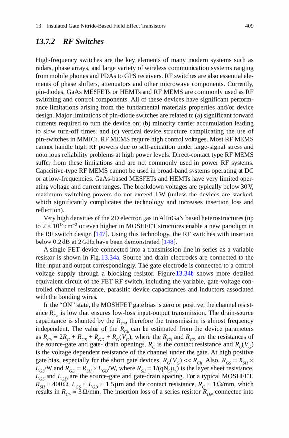
Recently novel type of RF switches employing capacitively-coupled contacts (C3) has been demonstrated as an efficient alternative to conventional transistor-based switches for high frequencies, above 2 GHz [60, 149, 150]. In C3 RF switches, the RF signal is injected via capacitive coupling between the metal electrode and the conducting channel, see Fig. 13.37; as a result no annealed ohmic contacts are required; hence the entire device or MMIC can be fabricated using self-aligned proc-ess. Effective contact impedance of C3-s can be as low as 0.1–0.4 Ω mm depending on frequency and epilayer structure.
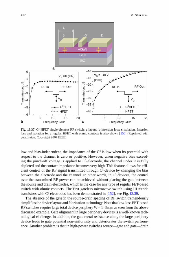
Flexible and robust C3 technology allows for a number of RF switch perform-ance improvements without significant technology complications. One example is multigate III-N RF switch demonstrated in [151]. Additional gates placed within a tight source-drain spacing of multigate C3—switch using fully self-aligned tech-nology, significantly improve the isolation and maximum switching power of RF switch (see Fig. 13.38).
An important feature of the C3 electrodes making them fundamentally different from regular ohmic contacts is the impedance dependence on the DC bias between the electrode and the device channel. Unlike ohmic contact, whose impedance is
Fig. 13.36 Frequency dependencies of insertion loss and isolation of the single-pole-single throw (SPST) switch. Solid lines—experimental data. Dotted line shows the simulated insertion loss in the absence of shunt HFET capacitance. Dashed line shows the simulated insertion loss in the absence of current crowding in the switch metal electrodes [148] (Reprinted with permission. Copyright 2008 IEEE)
Inse
rtio
n Lo
ss (
dB)
0.0
–0.2
–0.4
–0.6
–0.8
–1.0
Insertion loss
Isolation
0.5 1.0 1.5 2.0Frequency (GHz)
–10
–20
–30
–40
Isol
atio
n (d
B)
412 M. Shur et al.
low and bias-independent, the impedance of the C3 is low when its potential with respect to the channel is zero or positive. However, when negative bias exceed-ing the pinch-off voltage is applied to C3-electrode, the channel under it is fully depleted and the contact impedance becomes very high. This feature allows for effi-cient control of the RF signal transmitted through C3-device by changing the bias between the electrode and the channel. In other words, in C3-devices, the control over the transmitted RF power can be achieved without placing the gate between the source and drain electrodes, which is the case for any type of regular FET-based switch with ohmic contacts. The first gateless microwave switch using III-nitride transistors with C3 electrodes has been demonstrated in [152], see Fig. 13.39.
The absence of the gate in the source-drain spacing of RF switch tremendously simplifies the device layout and fabrication technology. Note that low-loss FET-based RF switches require large total device periphery W = 1–3 mm as seen from the above discussed example. Gate alignment in large periphery devices is a well-known tech-nological challenge. In addition, the gate metal resistance along the large periphery device leads to gate potential non-uniformity and deteriorates the switch perform-ance. Another problem is that in high-power switches source—gate and gate—drain
Fig. 13.37 C3 HFET single-element RF switch: a layout; b insertion loss; c isolation. Insertion loss and isolation for a regular HFET with ohmic contacts is also shown [150] (Reprinted with permission. Copyright 2007 IEEE)
L
S G D
AlGaN
GaN
SiC
Tran
smis
sion
, dB
Tran
smis
sion
, dB
0a
b c
–1
–2
–3
–4
–5
–65 10 15 20
Frequency GHz Frequency GHz
VG = 0 (ON)
RF In RF InRF Out RF Out
VG VG
C3HFET C3HFET
HFET HFET
–10
–15
–20
–25
–30
–35
–40
5 10 15 20
VG = –10 V
(OFF)
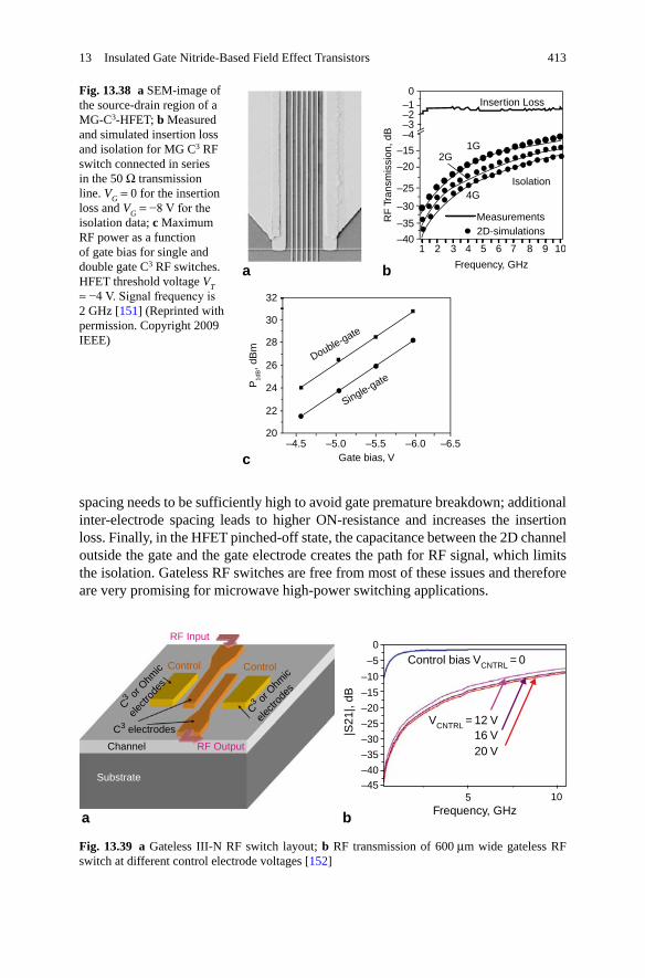
41313 Insulated Gate Nitride-Based Field Effect Transistors
spacing needs to be sufficiently high to avoid gate premature breakdown; additional inter-electrode spacing leads to higher ON-resistance and increases the insertion loss. Finally, in the HFET pinched-off state, the capacitance between the 2D channel outside the gate and the gate electrode creates the path for RF signal, which limits the isolation. Gateless RF switches are free from most of these issues and therefore are very promising for microwave high-power switching applications.
Fig. 13.38 a SEM-image of the source-drain region of a MG-C3-HFET; b Measured and simulated insertion loss and isolation for MG C3 RF switch connected in series in the 50 Ω transmission line. VG = 0 for the insertion loss and VG = −8 V for the isolation data; c Maximum RF power as a function of gate bias for single and double gate C3 RF switches. HFET threshold voltage VT ≈ −4 V. Signal frequency is 2 GHz [151] (Reprinted with permission. Copyright 2009 IEEE)
Double-gate
Single-gate
Gate bias, V
P1d
B, d
Bm
20–4.5 –5.0 –5.5 –6.0 –6.5
22
24
26
28
30
32
Insertion Loss
Isolation
Measurements2D-simulations
Frequency, GHz
1
RF
Tra
nsm
issi
on, d
B
–40
–35
–30
–25
–20
–15
–4–3–2–1
0
2G1G
4G
a b
c
1098765432
Fig. 13.39 a Gateless III-N RF switch layout; b RF transmission of 600 µm wide gateless RF switch at different control electrode voltages [152]
RF Input
Control Control
C3 o
r Ohm
ic
electr
odes
C3 o
r Ohm
ic
electr
odes
RF OutputChannel
Substrate
C3 electrodes |S21
|, dB
0
–5
–10
–15
–20
–25
–30
–35
–40
–45
Control bias VCNTRL = 0
VCNTRL = 12 V16 V20 V
5
a b
10Frequency, GHz
414 M. Shur et al.
13.7.3 Power Switches
GaN HFETs and especially MOSHFETs have tremendous potential for power electronic applications. The achievable switching power densities and breakdown voltages have been shown to be as high as 2.5 kV [153] and several kW/mm2 [18], respectively. A number of power converters using III-nitride HFETs have been dem-onstrated [154–156]. Monolithic high voltage GaN MOSFET/Schottky diode pair with the blocking capability ~1 kV has been demonstrated by [157]. Enhancement mode hybrid MOSFET/HFET devices demonstrated up to 70 A maximum drain cur-rent and blocking capability over 500 V [45]. The specific ON-resistance of this kind of hybrid switches can be as small as 20 mΩ cm2 or even smaller [45, 158]. The key advantage of MOSHFETs as compared to Schottky gate HFETs for power electron-ics is negligibly small gate currents. This advantage allows III-nitride MOSHFETs to be used in the circuits with significant gate voltage overshoots and eliminate additional protections circuits.
13.8 Future Trends: From Megawatts to Terahertz
Silicon CMOS dominate the electronics technology. Compared to Si CMOS, Si MESFETs or Si-Ge HFETs are niche technologies commanding with tiny market share. However, III-V insulated gate transistors have difficult time competing with their MESFET and HFET counterparts. This is because of additional interface states at the semiconductor-insulator interface. In the nitride materials system, the situation is completely different. Huge densities of the 2D electrons in the device channels mask the effects the interface states that are further diminished in MOSHFET struc-tures, where these interface states are separated from the active device channel by the wide band gap barrier layer. Moreover, the dielectric layer technology has proved to be necessary for the surface state passivation in the ungated regions for eliminating or reducing the current collapse (see Sect. 13.6) and improving lifetime and reliabil-ity. As mentioned above, the suppression of the gate leakage current eliminates one important mechanism of the device failure. GaN-based MOSHFETs already outper-form more conventional GaN-based HEMTs and have been commercialized [137].
Further progress will depend on better understanding of the new and complex device physics that involves interplay between the dielectric surface states in the gated and ungated regions [134] and on more advanced gate edge engineering to alleviate high field effects at the gate edges. Using high-k dielectric stacks, such as including HfO2, is especially promising. When this technology improves, we can expect reliable power microwave devices providing tens of watts of power at frequencies up to 60 GHz or more with unsurpassed efficiencies [144], power switches handling currents in the kilo ampere range and blocking voltages of a kilo-volt or more. GaN-MOSHFET switches will mostly replace RF MEMs because of extremely low insertion loss, excellent linearity, and a very high isolation.
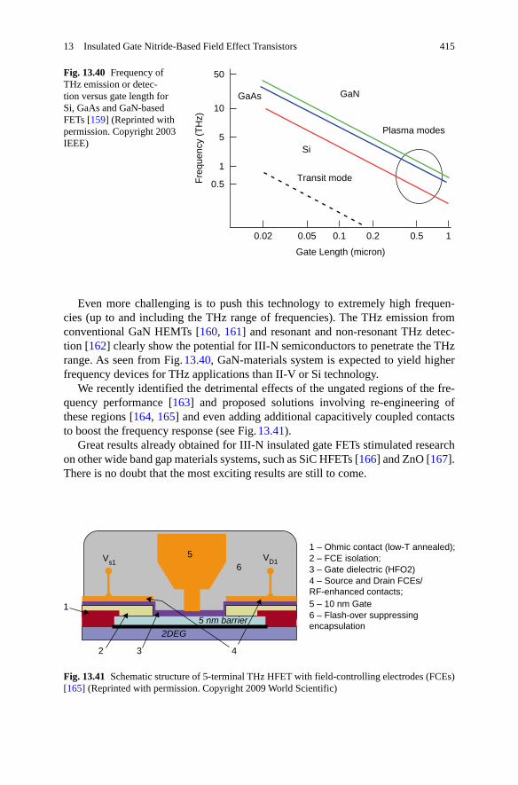
41513 Insulated Gate Nitride-Based Field Effect Transistors
Even more challenging is to push this technology to extremely high frequen-cies (up to and including the THz range of frequencies). The THz emission from conventional GaN HEMTs [160, 161] and resonant and non-resonant THz detec-tion [162] clearly show the potential for III-N semiconductors to penetrate the THz range. As seen from Fig. 13.40, GaN-materials system is expected to yield higher frequency devices for THz applications than II-V or Si technology.
We recently identified the detrimental effects of the ungated regions of the fre-quency performance [163] and proposed solutions involving re-engineering of these regions [164, 165] and even adding additional capacitively coupled contacts to boost the frequency response (see Fig. 13.41).
Great results already obtained for III-N insulated gate FETs stimulated research on other wide band gap materials systems, such as SiC HFETs [166] and ZnO [167]. There is no doubt that the most exciting results are still to come.
Fig. 13.40 Frequency of THz emission or detec-tion versus gate length for Si, GaAs and GaN-based FETs [159] (Reprinted with permission. Copyright 2003 IEEE)
GaN
Plasma modes
Si
GaAs
Transit modeFre
quen
cy (
TH
z)
0.5
1
5
10
50
Gate Length (micron)
0.02 0.05 0.1 0.2 0.5 1
Fig. 13.41 Schematic structure of 5-terminal THz HFET with field-controlling electrodes (FCEs) [165] (Reprinted with permission. Copyright 2009 World Scientific)
Vs15
6VD1
1
2 3 4
5 nm barrier
1 – Ohmic contact (low-T annealed);2 – FCE isolation;3 – Gate dielectric (HFO2)4 – Source and Drain FCEs/RF-enhanced contacts;5 – 10 nm Gate6 – Flash-over suppressingencapsulation
2DEG
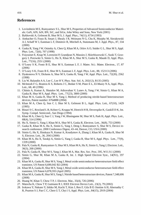
416 M. Shur et al.
References
1. Levinshtein M E, Rumyantsev S L, Shur M S, Properties of Advanced Semiconductor Materi-als: GaN, AlN, InN, BN, SiC, and SiGe, John Wiley and Sons, New York (2001)
2. Bykhovski A, Gelmont B, Shur M S, J. Appl. Phys., 74(11), 6734 (1993) 3. Ambacher O, Foutz B, Smart J, Shealy J R, Weimann N G, Chu K, Murphy M, Sierakowski
A J, Schaff W J, Eastman L F, Dimitrov R, Mitchell A, Stutzmann M, J. Appl. Phys., 87, 334 (2000)
4. Gaska R, Yang J W, Osinsky A, Chen Q, Khan M A, Orlov A O, Snider G L, Shur M S, Appl. Phys. Lett., 72(6), 707 (1998)
5. Frayssinet E, Knap W, Lorenzini P, Grandjean N, Massies J, Skierbiszewski C, Suski T, Grze-gory I, Porowski S, Simin G, Hu X, Khan M A, Shur M S, Gaska R, Maude D, Appl. Phys. Lett., 77(16), 2551 (2000)
6. O’Leary S K, Foutz B E, Shur M S, Eastman L F, J. Mater. Sci.: Mater. Electron., 17, 87 (2006)
7. O’Leary S K, Foutz B E, Shur M S, Eastman L F, Appl. Phys. Lett., 88, 152113 (2006) 8. Dyakonova N V, Dickens A, Shur M S, Gaska R, Yang J W, Appl. Phys. Lett., 72(20), 2562
(1998) 9. Liu W, Balandin A A, Lee C, Lee H Y, Phys. Stat. Sol. A, 202(12), R135 (2005)10. McIntosh F G, Boutros K S, Roberts J C, Bedair S M, Piner E L, El-Masry N A, Appl. Phys.
Lett., 68, 40 (1996)11. Chitnis A, Kumar A, Shatalov M, Adiravahan V, Lunev A, Yang J W, Simin G, Khan M A,
Gaska R, Shur M S, Appl. Phys. Lett., 77(23), 3800 (2000)12. Khan M A, Gaska R, Shur M S, Yang J, Method of producing nitride-based heterostructure
devices, Patent number: 6764888 (2004)13. Khan M A, Chen Q, Sun C J, Shur M S, Gelmont B L, Appl. Phys. Lett., 67(10), 1429
(1995)14. Binari S C, Rowland L B, Kelner G, Kruppa W, Dietrich H B, Doverspike K, Gaskill D K, Int.
Symp. Compd. Semicond., San Diego (1994)15. Khan M A, Chen Q, Sun C J, Yang J W, Blasingame M, Shur M S, Park H, Appl. Phys. Lett.,
68(4), 514 (1996)16. Hu X, Simin G, Yang J, Khan M A, Shur M S, Gaska R, Electron. Lett., 36(8), 753 (2000)17. Gaska R, Khan M A, Hu X, Simin G, Yang J, Deng J, Rumyantsev S, Shur M S, Device re-
search conference, 2000 Conference Digest, 43–44, Denver, CO, USA (2000)18. Simin G, Hu X, Ilinskaya N, Kumar A, Koudymov A, Zhang J, Khan M A, Gaska R, Shur M
S, Electron. Lett., 36, 2043 (2000)19. Khan M A, Hu X, Tarakji A, Simin G, Yang J, Gaska R, Shur M S, Appl. Phys. Lett., 77(9),
1339 (2000)20. Pala N, Gaska R, Rumyantsev S, Shur M S, Khan M A, Hu X, Simin G, Yang J, Electron. Lett.,
36(3), 268 (2000)21. Pala N, Gaska R, Shur M S, Yang J, Khan M A, Mat. Res. Soc. Proc, 595, W11.9.1 (2000)22. Simin G, Shur M, Khan M A, Gaska R, Int. J. High Speed Electron Syst., 14(N1), 197
(2004)23. Khan M A, Gaska R, Shur M S, Yang J, Metal oxide semiconductor heterostructure field effect
transistor, US Patent 6,690,042 B2 (2004)24. Khan M A, Gaska R, Shur M S, Yang J, Metal oxide semiconductor heterostructure field effect
transistor, US Patent 6,878,593 (April 2005)25. Khan M A, Gaska R, Shur M S, Yang J, Nitride based heterostructure devices, Patent 7,348,606
(2008)26. Huang W, Khan T, Chow T P, J. Electron. Mat., 35(4), 726 (2006)27. Matocha K, Chow T P, Gutmann R J, IEEE Electron Device Lett., 23(2), 79 (2002)28. Irokawa Y, Nakano Y, Ishiko M, Kachi T, Kim J, Ren F, Gila B P, Onstine A H, Abernathy C
R, Pearton S J, Pan C C, Chen G T, Chyi J I, Appl. Phys. Lett., 84(15), 2919 (2004)
41713 Insulated Gate Nitride-Based Field Effect Transistors
29. Matocha K, Chow T P, Gutmann R J, IEEE Trans. Electron Devices, 52(1), 6 (2005)30. Jang S, Ren F, Pearton S J, Gila B P, Hlad M, Abernathy C R, Yang H, Pan C J, Chyi J I, Bove
P, Lahreche H, Thuret J, J. Electron. Mater., 35(4), 685 (2006)31. Lee H B, Cho H I, An H S, Bae Y H, Lee M B, Lee J H, Hahm S H, IEEE Electron Device
Lett., 27(2), 81 (2006)32. Huang W, Khan T, Chow T P, IEEE Electron Device Lett., 27, 796 (2006)33. Huang W, Chow T P, Khan T, Phys. Stat. Sol. A, 204(6), 2064 (2007)34. Kambayashi H, Niiyama Y, Ootomo S, Nomura T, Iwami M, Satoh Y, Kato S, Yoshida S,
IEEE Electron Device Lett., 28(12), 1077 (2007)35. Chow T P, Naik H, Li Z, Phys. Stat. Sol. A, 1, doi: 10.1002 (2009)36. Tokranov V, Rumyantsev S L, Shur M S, Gaska R, Oktyabrsky S, Jain R, Pala N, Phys. Stat.
Sol. (RRL), 1(5), 199 (2007)37. Morkoç H, J. Mater. Sci.: Mater. Elect., 12(12), 677 (2001)38. Pei Y, Poblenz C, Cordon A L, Chu R, Shen L, Speck J S, Mishra U K, Electron Lett., 44(9),
598 (2008)39. Fareed Q, Gaska R, Shur M S, Methods of growing Nitride-based film using varying pulses,
US Patent 7192849 (2007)40. Zhang J P, Kuokstis E, Fareed Q, Wang H M, Yang J W, Simin G, Khan M A, Tamulaitis G,
Kurilcik G, Jursenas S, Zukauskas A, Gaska R, Shur M, Phys. Stat. Sol. A, 188, 95 (2001)41. Kazlauskas K, Žukauskas A, Tamulaitis G, Mickevičius J, Shur M S, Fareed R S Q, Zhang J
P, Gaska R, Appl. Phys. Lett., 87, 172102 (2005)42. Khan M A, Yang J W, Knap W, Frayssinet E, Hu X, Simin G, Prystawko P, Leszczynski M,
Grzegory I, Porowski S, Gaska R, Shur M S, Beaumont B, Teisseire M, Neu G, Appl. Phys. Lett., 76(25), 3807 (2000)
43. Hu X, Deng J, Pala N, Gaska R, Shur M S, Chen C Q, Yang J, Simin G, Khan M A, Rojo J C, Schowalter L J, Appl. Phys. Lett., 82, 1299 (2003)
44. Matocha K, Chow T P, Gutmann R J, 15th Int. Symp. Power Semicond. Devices ICs, ISPSD 2003, 54 (2003)
45. Kambayashi H, Satoh Y, Niiyama Y, Kokawa T, Iwami M, Nomura T, Kato S, Chow T P, 21st Int. Symp. Power Semicond. Devices ICs, ISPSD 2009, 21 (2009)
46. Liu L, Edgar J H, Mater. Sci. Eng. R, 37, 61 (2002)47. Sheppard S T, Smith R P, Pribble W L, Ring Z, Smith T, Allen S T, Milligan J, Palmour J W,
Dev. Res. Conf., Cat. No. 02TH8606, 175 (2002)48. Rajagopal P, Roberts J C, Cook J W, Jr., Brown J D, Piner E L, Linthicum K J, Mater. Res. Soc.
Symp. Proc., 798, Y7.2.1 (2003)49. Johnson J W, Piner E L, Vescan A, Therrien R, Rajagopal P, Roberts J C, Brown J D, Singhal
S, Linthicum K J, IEEE Electron Device Lett., 25, 459 (2004)50. Khan M A, Simin Shur M S, Gaska R, Electronic device based on group III Nitrides. In:
Buschow K H J, Cahn R W, Flemings M C, Ilschner B, Kramer E J, Mahajan S (eds) Encyclo-pedia of Materials: Science and Technology, 3, 2616 (2008)
51. Wetzel C, Suski T, Ager JW, III, Weber E R, Haller E E, Fisher S, Meyer B K, Molnar R J, Perlin P, Phys. Rev. Lett., 78, 3923 (1997)
52. Hubbard S M, Zhao G, Pavlidis D, Sutton W, Cho E, Mater. Res. Soc. Symp. Proc., 831, E11.11.1 (2004)
53. Haffouz S, Tang H, Bardwell J A, Hsu E M, Webb J B, Rolfe S, Solid-State Electron, 49(5), 802 (2005)
54. Iliopoulos E, Zervos M, Adikimenakis A, Tsagaraki K, Georgakilas A, Superlattices Micro-struct., 40(4–6), 313 (2006)
55. Gu X, Izyumskaya N, Avrutin V, Xie J, Chevtchenko S, Xiao B, Morkoç H, Proc. SPIE, 6473, 64730S (2007)
56. Wu H M, Peng L H, Phys. Stat. Sol. C, 3(6), 2291 (2006)57. Ren F, Hong M, Chu S N G, Marcus M A, Schurman M J, Baca A, Pearton S J, Abernathy C
R, Appl. Phys. Lett., 73, 3893 (1998)58. Wu Y Q, Ye P D, Wilk G D, Yang B, Mater. Sci. Eng. B, 135, 282 (2006)

418 M. Shur et al.
59. Liu C, Chor E F, Tan L S, Appl. Phys. Lett., 88, 173504 (2006)60. Koudymov A, Pala N, Tokranov V, Oktyabrsky S, Gaevski M, Jain R, Yang J, Hu X, Shur M,
Gaska R, Simin G, IEEE Electron Device Lett., 30(5), 433 (2009)61. Koudymov A, Pala N, Tokranov V, Oktyabrsky S, Gaevski M, Jain R, Yang J, Hu X, Shur M
S, Gaska R, Simin G, IEEE Electron Device Lett., 30, 478 (2009)62. Littlejohn M A, Hauser J R, Glisson T H, Appl. Phys. Lett., 26, 625 (1975)63. Gelmont B, Kim K, Shur M, J. Appl. Phys., 74, 1818 (1993)64. Mansour N S, Kim K W, Littlejohn M A, J. Appl. Phys., 77, 2834 (1995)65. KolnıK J, Oguzman I H, Brennan K F, Wang R, Ruden P P, Wang Y, J. Appl. Phys., 78, 1033
(1995)66. Foutz B E, Eastman L F, Bhapkar U V, Shur M S, Appl. Phys. Lett., 70, 2849 (1997)67. Bhapkar U V, Shur M S, J. Appl. Phys., 82, 1649 (1997)68. Albrecht J D, Wang R P, Ruden P P, Farahmand M, Brennan K F, J. Appl. Phys., 83, 4777
(1998)69. Foutz B E, O’Leary S K, Shur M S, Eastman L F, J. Appl. Phys., 85, 7727 (1999)70. O’Leary S K, Foutz B E, Shur M S, Eastman L F, J. Electron Mater., 32, 327 (2003)71. O’Leary S K, Foutz B E, Shur M S, Bhapkar U V, Eastman L F, Solid State Commun., 105,
621 (1998)72. Albrecht J D, Wang R P, Ruden P P, Farahmand M, Brennan K F, J. Appl. Phys., 83, 1446
(1998)73. O’Leary S K, Foutz B E, Shur M S, Bhapkar U V, Eastman L F, J. Appl. Phys., 83, 826
(1998)74. Bellotti E, Doshi B K, Brennan K F, Albrecht J D, Ruden P P., J. Appl. Phys., 85, 916 (1999)75. Vasconcelos T F, Maia F F, Jr., Caetano E W S, Freire V N, da Costa J A P, da Silva E F, Jr., J.
Cryst. Growth, 246, 320 (2002)76. O’Leary S K, Foutz B E, Shur M S, Eastman L F, J. Mater. Sci. Mater. Electron, doi: 10.1007/
s10854-009-9896-1 (2009)77. Oberhuber R, Zandler G, Vogl P, Appl. Phys. Lett., 73, 818 (1998)78. Krishnan M S, Goldsman N, Christou A, J. Appl. Phys., 83, 5896 (1998)79. Heying B, Smorchkova I, Poblenz C, Elsass C, Fini P, DenBaars S, Mishra U, Speck J S, Appl.
Phys. Lett., 77, 2885 (2000)80. Saxler A, Look D C, Elhamri S, Sizelove J, Cull D, Mitchel W C, Callahan M, Bliss D,
Bouthillette L, Wang S Q, Sung C M, Lee K Y, GaN and Related Alloys, Mater. Res. Soc. Symp. Proc., 639 (2000)
81. Look D C, Sizelove J R, Appl. Phys. Lett., 79, 1133 (2001)82. Ambacher O, Smart J, Shealy J R, Weimann N G, Chu K, Murphy M, Schaff W J, Eastman
L F, Dimitrov R, Wittmer L, Stutzmann M, Rieger W, Hilsenbeck J, J. Appl. Phys., 85, 3222 (1999)
83. Bernardini F, Fiorentini V, Vanderbilt D, Phys. Rev. B., 56, R10024 (1997)84. Smorchkova I P, Elsass C R, Ibbetson J P, Vetury R, Heying B, Fini P, Haus E, DenBaars S P,
Speck J S, Mishra U K, J. Appl. Phys., 86, 4520 (1999)85. Smorchkova I P, Chen L, Mates T, Shen L, Heikman S, Moran B, J. Appl. Phys., 90, 5196
(2001)86. Shur M S, Bykhovski A D, Gaska R, Solid-State Electron, 44, 205 (2000)87. Liberis J, Matilioniene I, Matulionis A, Sermunksnis E, Xie J, Leach J H, Morkoc H, Phys.
Stat. Sol. A, 206, 1385 (2009)88. Gaska R, Shur M S, Bykhovski A D, Orlov A O, Snider G L, Appl. Phys. Lett., 74(2), 287
(1999)89. Aggerstam T, Lourdudoss S, Radamson H H, Sjödin M, Lorenzini P, Look D C, Thin Solid
Films, 515, 705 (2006)90. Ivanov P A, Levinshtein M E, Simin G, Hu X, Yang J, Khan M A, Rumyantsev S L, Shur M
S, Gaska R, Electron. Lett., 37(24), 1479 (2001)91. Huang W, Chow T P, Niiyama Y, Nomura T, Yoshida S, 21st Int. Symp. Power Semicond.
Devices IC’s, ISPSD 2009. 29 (2009)
41913 Insulated Gate Nitride-Based Field Effect Transistors
92. Binari S C, Dietrich H B, Kruppa W, Kelner G, Saks N S, Edwards A, Redwing J M, Wick-enden A E, Koleske D D, Proc. 2nd Int. Conf. Nitride Semicond. (ICNS 97), 476 (1997)
93. Ochiai M, Akita M, Ohno Y, Kishimoto S, Maezawa K, Mizutani T, Jpn. J. Appl. Phys., 42, 2278 (2003)
94. Ye P D, Yang B, Ng K K, Bude J, Wilk G D, Halder S, Hwang J C M, Appl. Phys. Lett., 86, 063501 (2005)
95. Mehandru R, Luo B, Kim J, Ren F, Gila B P, Onstine A H, Abernathy C R, Pearton S J, Gotthold D, Birkhahn R, Peres B, Fitch R, Gillespie J, Jenkins T, Sewell J, Via D, Crespo A, Appl. Phys. Lett., 82, 2530 (2003)
96. Rai S, Adivarahan V, Huang P, Tipirneni N, Husna F, Simin G, Yang J W, Khan M A, Jpn. J. Appl. Phys., 45(6A), 4985 (2006)
97. Khan M A, Shur M S, Chen Q C, Kuznia J N, Electron. Lett., 30(25), 2175 (1994) 98. Cho D, Shimizu M, Ide T, Ookita H, Okumura H, Jpn. J. Appl. Phys. V., 41, 4481 (2002) 99. Mohammed F M, Wang L, Koo H J, Adesida I, J. Appl. Phys., 101, 033708 (2007)100. Das J, Oprins H, Ji H, Sarua A, Ruythooren W, Derluyn J, Kuball M, Germain M, Borghs G,
IEEE Trans. Electron Devices, 53(11), 2696 (2006)101. Binari S C, Rowland L B, Kelner G, Kruppe W, Dietrich H B, Doverspike K, Gaskill D K,
Int. Symp. Compound Semicond., Bristol, UK: IOP, 459 (1995)102. Koudymov A, Fatima H, Simin G, Yang J, Khan M A, Tarakji A, Hu X, Shur M S, Gaska R,
Appl. Phys. Lett., 80, 3216 (2002)103. Shur M S, GaAs Devices and Circuits, Plenum Press, New York and London (1987)104. Clarke F W, Ho F D, Khan M A, Simin G, Yang J, Gaska R, Shur M S, Deng J, Karmalkar S,
Mat. Res. Symp. Proc., 743, L 9.10 (2002)105. Karmalkar S, Sathaiya D M, Shur M S, Appl. Phys. Lett., 82, 3976–3978 (2003)106. Simin G, Tarakji A, Hu X, Koudymov A, Yang J, Khan M A, Shur M S, Gaska R, Phys. Stat.
Sol. A, 188(1), 219 (2001)107. Tarakji A, Hu X, Koudymov A, Simin G, Yang J, Khan M A, Shur M S, Gaska R, Solid-State
Electron, 46(8), 1211 (2002)108. Simin G, Hu X, Ilinskaya N, Zhang J, Tarakji A, Kumar A, Khan M A, Gaska R, Shur M S,
IEEE Electron Device Lett., 22(2), 53 (2001)109. Copeland J A, IEEE Trans. Electron Devices, 18, 50 (1971)110. Levinshtein M E, Rumyantsev S L, Semicond. Sci. Tech., 9(6), 1183 (1994)111. Rumyantsev S L, Pala N, Shur M S, Borovitskaya E, Dmitriev A P, Levinshtein M E, Gaska
R, Khan M A, Yang J, Hu X, Simin G, IEEE Trans. Electron Devices, 48(3), 530 (2001)112. Pala N, Rumyantsev S, Shur M S, Gaska R, Hu X, Yang J, Simin G, Khan M A, Fluct. Noise
Lett., 2(4), L349 (2002)113. Rumyantsev S L, Pala N, Shur M S, Levinshtein M E, Gaska R, Khan M A, Simin G, Genera-
tion—Recombination noise in GaN-based devices. In: Shur M S, Davis R F (ed), GaN-Based Materials and Devices, Selected Topics in Electronics and Systems, World Scientific, 33 (2004)
114. Levinshtein M E, Balandin A A, Rumyantsev S L, Shur M S, Low-frequency noise in GaN-based field effect transistors. In: Balandin A A (ed), Noise and Fluctuations Control in Elec-tronic Devices, American Scientific Publishers (2002)
115. Surya C, Fong W K, Leung B H, Material processing and low frequency noise in GaN thin films and devices. In: Balandin A A (ed), Noise and Fluctuations Control in Electronic De-vices, American Scientific Publishers (2002)
116. Levinshtein M E, Rumyantsev S L, Shur M S, Gaska R, Khan M A, Spec. Issue IEE Proc. Circuits Devices Syst., 149(1), 32 (2002)
117. Rumyantsev S L, Pala N, Shur M S, Gaska R, Levinshtein M E, Khan M A, Simin G, Hu X, Yang J, J. Appl. Phys., 88(11), 6726 (2000)
118. McWhorter A L, Proc. Conf. Phys. Semicond. Surf., Philadelphia, 207 (1956)119. Christensson S, Lundstrom I, Svensson C, Solid-State Electron., 11, 797 (1968)120. Morshed T H, Devireddy S P, Celik-Butler Z, Shanware A, Green K, Chambers J J, Visokay
M R, Colombo L, Solid-State Electron., 52, 711 (2008)

420 M. Shur et al.
121. Rumyantsev S, Young C, Bersuker G, Shur M, 20th Int. Conf. Noise Fluct., ICNF 2009, Pisa, Italy, AIP Conf. Proc., 1129, 255 (2009)
122. Chiou Y Z, Su Y K, Gong J, Chang S J, Wang C K, Jpn. J. Appl. Phys. V., 45(4B), 3405 (2006)
123. Rumyantsev S L, Pala N, Shur M S, Gaska R, Levinshtein M E, Khan M A, Simin G, Hu X, Yang J, J. Appl. Phys., 90(1), 310 (2001)
124. Simin G, Koudymov A, Tarakji A, Hu X, Yang J, Khan M A, Shur M S, Gaska R, Appl. Phys. Lett., 79, 2651 (2001)
125. Pala N, Rumyantsev S L, Shur M S, Hu X, Tarakji A, Gaska R, Khan M A, Simin G, Yang J, Solid State Electron., 46, 711 (2002)
126. Vetury R, Zhang N Q, Keller S, Mishra U K, IEEE Trans. Electron Devices, 48, 560 (2001)127. Binari S C, Klein P, Kazior T, Proc. IEEE, 90, 1048 (2002)128. Green B M, Chu K K, Chumbes E M, Smart J A, Shealy J R, Eastman L F, IEEE Electron
Device Lett., 21, 268 (2000)129. Arulkumaran S, Egawa T, Ishikawa H, Jimbo T, Sano Y, Appl. Phys. Lett., 84, 613 (2004)130. Braga N, Mickevicius R, Rao V, Fichtner W, 16th Biennial University Government Industry
Microelectronics Symposium, San Jose, CA (2006)131. Ando Y, Okamoto Y, Miyamoto H, Nakayama T, Inoue T, Kuzuhara M, IEEE Electron De-
vice Lett., 24, 289 (2003)132. Karmalkar S, Shur M S, Simin G, Khan M A, IEEE Trans. Electron Devices, 52, 2534
(2005)133. Koudymov A, Wang C X, Adivarahan V, Yang J, Simin G, Khan M A, IEEE Electron Device
Lett., 28, 5 (2007)134. Koudymov A, Shur M, Int. J. High Speed Electron. Syst., 18(4), 935 (2008)135. Adivarahan V, Yang J, Koudymov A, Simin G, Khan M A, IEEE Electron Device Lett.,
26(8), 535 (2005)136. Saygi S, Fatima H, He X, Rai S, Koudymov A, Adivarahan V, Yang J, Simin G, Khan M A,
Phys. Stat. Sol. (c), 2(7), 2651 (2005)137. Kanamura M, Kikkawa T, Iwai T, Imanishi K, Kubo T, Joshin K, Electron Devices Meeting,
2005, IEDM Tech. Dig., 5, 572 (2005)138. Mishra U, Shen L, Kazior T E, Wu Y F, Proc. IEEE, 96, 287 (2008)139. Simin G, Adivarahan V, Yang J, Koudymov A, Rai S, Khan M A, Electron Lett., 41(13), 774
(2005)140. Wu Y F, Saxler A, Moore M, Smith R P, Sheppard S, Chavarkar P M, Wisleder T, Mishra U
K, Parikh P, IEEE Electron Device Lett., 25, 117 (2004)141. Cripps S C, Advanced Techniques in RF Power Amplifier Design, Artech House, Boston/
London (2002)142. Gaska R, Yang J, Osinsky A, Khan M A, Shur M S, IEDM-97 Tech. Dig., 565 (1997)143. Saito W, Domon T, Omura I, Kuraguchi M, Takada Y, Tsuda K, Yamaguchi M, IEEE Elec-
tron Device Lett., 27, 326 (2006)144. Koudymov A, Shur M, Two-stage amplification using intermediate non-linear square wave,
US Patent 7,560,985 (2009)145. Braga N, Mickevicius R, Fichtner W, Gaska R, Shur M S, 2005 IEEE CSICS Tech. Dig.,
Palm Springs, CA, 149 (2005)146. Nakajima A, Itagaki K, Horio K, IEEE International Reliability Physics Symposium, 722
(2009)147. Simin G, Khan M A, Shur M S, Gaska R, Int. J. High Speed Electron Syst., 16(N2), 455
(2006)148. Yang Z, Wang J, Hu X, Yang J, Simin G, Shur M, Gaska R, IEEE Electron Device Lett., 29,
15 (2008)149. Simin G, Yang Z J, Koudymov A, Adivarahan V, Yang J, Khan M A, Appl. Phys. Lett., 89,
033510 (2006)150. Simin G, Yang G, Shur M, IEEE/MTT-S Int. Microwave Symp., 457 (2007)

42113 Insulated Gate Nitride-Based Field Effect Transistors
151. Hu X, Gaevski M, Khan B, Wang J, Gaska R, Simin G, Koudymov A, Jain R, Yang J, Shur M, IEEE Electron Device Lett., 30(9), 895 (2009)
152. Simin G, Wang J, Koudymov A, Sattu A, Yang J, Shur M, Gaska R, 33rd Workshop on Com-pound Semiconductor Devices and Integrated Circuits, WOCSDICE 2009, Málaga (Spain), Extended Abstract Book, Sect. Monday 5, 10 (2009)
153. Huang W, Chow T P, Niiyama Y, Nomura T, Yoshida S, 20th Int. Symp. Power Semicond. Devices IC’s, ISPSD 2008, 291 (2008)
154. Zhang N Q, Moran B, DenBaars S P, Mishra U K, Wang X W, Ma T P, Phys. Stat. Sol. A, 188(1), 213 (2001)
155. Pytel S G, Lentijo S, Rai S, Fatima H, Adivarahan V, Chitnis A, Yang J, Hudgins J L, Santi E, Monti A, Simin G, Khan M A, Power Electron. Spec. Conf. 2004 IEEE 35th Annual, 1, 579 (2004)
156. Saito W, Kuraguchi M, Takada Y, Tsuda K, Omura I, Ogura T, IEEE Trans. Electron Devices, 51, 1913 (2004)
157. Huang W, Chow T P, Proc. 19th Int. Symp. Power Semicond. Devices ICs, 265 (2007)158. Huang W, Li Z, Chow T P, Niiyama Y, Nomura T, Yoshida S, 20th Int. Symp. Power Semi-
cond. Devices IC’s, ISPSD 2008, 295 (2008)159. Ryzhii V, Shur M S, ISDRS Digest, Washington DC, WP7-07-10, 200 (2003)160. Deng Y, Kersting R, Xu J, Ascazubi R, Zhang X C, Shur M S, Gaska R, Simin G S, Khan M
A, Ryzhii V, Appl. Phys. Lett., 84(15), 70 (2004)161. Dyakonova N, Fatimy A E, Lusakowski J, Knap W, Dyakonov M I, Poisson M A, Morvan E,
Bollaert S, Shchepetov A, Roelens Y, Gaquiere Ch, Theron D, Cappy A, Appl. Phys. Lett., 88(14), 141906 (2006)
162. Fatimy A E, Tombet S B, Teppe F, Knap W, Veksler D B, Rumyantsev S, Shur M.S, Pala N, Gaska R, Fareed Q, Hu X, Seliuta D, Valusis G, Gaquiere C, Theron D, Cappy A, Electron. Lett., 42(23), 1342 (2006)
163. Turin V O, Shur M S, Veksler D B, Int. J. High Speed Electron. Syst., 17(1), 19 (2007)164. Pala N, Yang J Z, Koudymov A, Hu X, Deng J, Gaska R, Simin G, Shur M S, Device Re-
search Conference, 2007 65th Annual, 43 (2007)165. Simin G, Shur M, Gaska R, Int. J High Speed Electron Syst., 19(1), 7 (2009)166. Chandrashekhar M V S, Thomas C I, Lu J, Spencer M G, Appl. Phys. Lett., 91, 033503
(2007)167. O’Leary S K, Foutz B E, Shur M S, Eastman L F, Appl. Phys. Lett., (2009, Submitted)