Inner Tracker Upgradedarbo/RD_FASE2/15-02-10_GD_RD_FASE2.D2.pdf · o G. Darbo – INFN / Genova...
28
o Inner Tracker Upgrade G. Darbo – INFN / Genova Milano, 10 February 2015 Inner Tracker Upgrade X Workshop ATLAS Italia 10 – 12 February 2015 G. Darbo – INFN / Genova Indico: https://agenda.infn.it/conferenceDisplay.py?confId=8955
Transcript of Inner Tracker Upgradedarbo/RD_FASE2/15-02-10_GD_RD_FASE2.D2.pdf · o G. Darbo – INFN / Genova...

o Inner Tracker Upgrade G. Darbo – INFN / Genova Milano, 10 February 2015
Inner Tracker Upgrade
X Workshop ATLAS Italia10 – 12 February 2015
G. Darbo – INFN / Genova
Indico: https://agenda.infn.it/conferenceDisplay.py?confId=8955
Inner Tracker Upgrade G.Darbo – INFN / Genova Milano, 10 February 2015 2
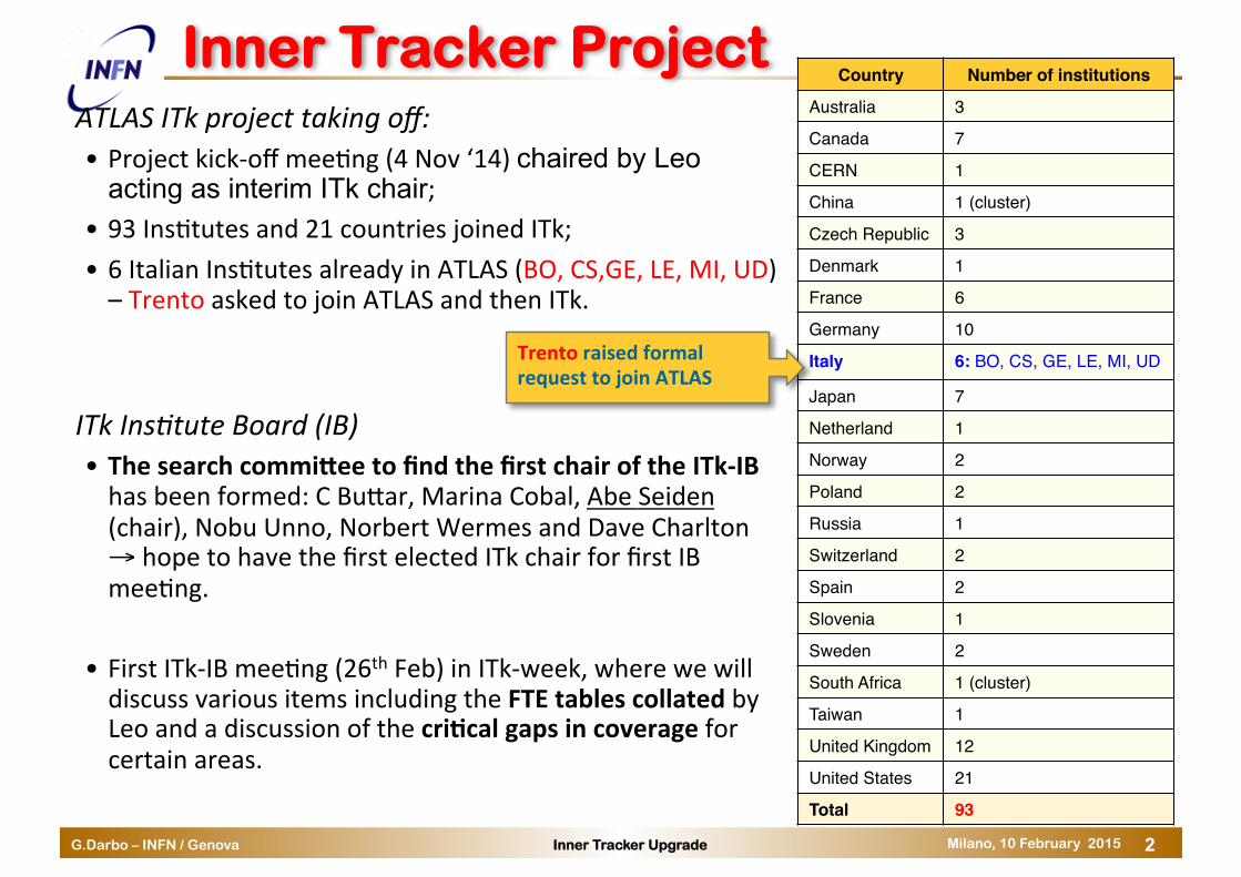
Inner Tracker Project ATLAS ITk project taking off: • Project kick-‐off mee/ng (4 Nov ‘14) chaired by Leo
acting as interim ITk chair; • 93 Ins/tutes and 21 countries joined ITk; • 6 Italian Ins/tutes already in ATLAS (BO, CS,GE, LE, MI, UD) – Trento asked to join ATLAS and then ITk.
ITk Ins6tute Board (IB) • The search commi,ee to find the first chair of the ITk-‐IB has been formed: C BuXar, Marina Cobal, Abe Seiden (chair), Nobu Unno, Norbert Wermes and Dave Charlton → hope to have the first elected ITk chair for first IB mee/ng.
• First ITk-‐IB mee/ng (26th Feb) in ITk-‐week, where we will discuss various items including the FTE tables collated by Leo and a discussion of the cri:cal gaps in coverage for certain areas.
Country Number of institutions
Australia 3
Canada 7
CERN 1
China 1 (cluster)
Czech Republic 3
Denmark 1
France 6
Germany 10
Italy 6: BO, CS, GE, LE, MI, UD
Japan 7
Netherland 1
Norway 2
Poland 2
Russia 1
Switzerland 2
Spain 2
Slovenia 1
Sweden 2
South Africa 1 (cluster)
Taiwan 1
United Kingdom 12
United States 21
Total 93
Trento raised formal request to join ATLAS

Inner Tracker Upgrade G.Darbo – INFN / Genova Milano, 10 February 2015 3
ITk Scoping Scenario • LHCC requests a cost document for ATLAS Phase II with possible de-‐scoping
§ 2-‐4 Jun – First dra_ to LHCC § 1 Aug – Final dra_ to ATLAS § 22-‐24 Sep – Final document discussed by LHCC § 26-‐28 Oct – Final presenta/on to RRB
• ATLAS mandate a subgroup of the USC to study 3 scenarios: 275, 235 and 200 MCHF (old CHF rate!).
• For ITk too short 6me to focus on “preferred” layout (many under study → see Layout TF). • Concentrate on LoI layout + extension at η = 4 • For ITk should be considered as pure exercise: not what we are going to build, but how performance goes with de-‐scoping
• Effort must be coherent with CMS

Inner Tracker Upgrade G.Darbo – INFN / Genova Milano, 10 February 2015 4
ITk “275” layout
• LoI + Very Forward extension to η = 4 Cost
Strips 95.7 M Pixel 24.8 M Common 11.0 M VF extension 12.0 M Savings (wrt LoI) -‐8.7 M ––––––––––––––––––––––––– Total 134.8 M
Ref.: P. MoreZni – R&D Phase II Italia – 23/1/2015

Inner Tracker Upgrade G.Darbo – INFN / Genova Milano, 10 February 2015 5
ITk “235” layout
WRT “275”: • VF extension only to η=3.2 • Strip “stub” layer removed
Cost “275” 134.8 M VF to h=3.2 -‐6.0 M Stub -‐2.0 M ––––––––––––––––––––––––– Total 126.8 M
Ref.: P. MoreZni – R&D Phase II Italia – 23/1/2015

Inner Tracker Upgrade G.Darbo – INFN / Genova Milano, 10 February 2015 6
ITk “200” layout
WRT “275”: • VF extension only to η=3.2 • 1 strip barrel and 1 disk set removed • 2 strip barrel single layer (not stereo)
Ref.: P. MoreZni – R&D Phase II Italia – 23/1/2015
Cost “275” 134.8 M VF to h = 3.2 -‐6.0 M 1 barrel+1disk -‐24.0 M 2 barrel layers -‐7.0 M ––––––––––––––––––––––––– Total 97.8 M

Inner Tracker Upgrade G.Darbo – INFN / Genova Milano, 10 February 2015 7
Layout TF Work Model
ITk Layout Tasks Force
• New Task Force (Claudia e Andy Salzburger chairs), with mandate to define the ITk layout → go to 2 (or 3) op6ons, by end 2015.
• Need help for simula6on (interes6ng task for young people too).
To study: § Local supports for layers 3-‐4
(inclined planes, like “alpine” → less silicon and material)
§ Look at extra pixel layer(s) with cheaper technologies to replace strips.
§ Realis:c simula:on of services and rou:ngs.
§ R/O sizing based on detector characteris:cs.
Ref.: P. MoreZni – R&D Phase II Italia – 23/1/2015

Inner Tracker Upgrade G.Darbo – INFN / Genova Milano, 10 February 2015 8
SLIM – Stiff Longeron for ITk Staves
IP Barrel Cells Tilted Cells
Connec/ng Structure
5th pixel layer inside the PST – HV-‐CMOS “op/mized” – 2.5 m long at layer 5.
one slim stave is equivalent to two adjacent conven/onal staves
Ref.: S. Michal, ITk Pixel Design Group, 29/01/2015

Inner Tracker Upgrade G.Darbo – INFN / Genova Milano, 10 February 2015 9
SLIM – Material Budget
Slide 33 January, 27th 2014 Sébastien MICHAL
0.00
0.50
1.00
1.50
2.00
2.50
3.00
3.50
4.00
0.0 0.5 1.0 1.5 2.0 2.5
%X
/X0
BARREL vs TILTED 2.5 m
8 per. Mov. Avg. (TILTED DET SLIM MOY TOT %X/X0PER DEGREE)8 per. Mov. Avg. (BARREL DET SLIM MOY TOT %X/X0PER DEGREE)
2.5m FULL BARREL vs TILTED SLIM • Only the structural cells are studied • The longer the stave, the better it is
Barrel to tilted cell
Eta
Lower surface and consequently lower cost �22 % less for a 1.5 m stave at layer 5 �39 % less for a 2.5 m stave at layer 5 Note: only structural cells studied
Ref.: S. Michal, ITk Pixel Design Group, 29/01/2015

Inner Tracker Upgrade G.Darbo – INFN / Genova Milano, 10 February 2015 10
RD_FASE2 Tracker R&D in CSN1
Inner Tracker Upgrade G.Darbo – INFN / Genova Milano, 10 February 2015 11
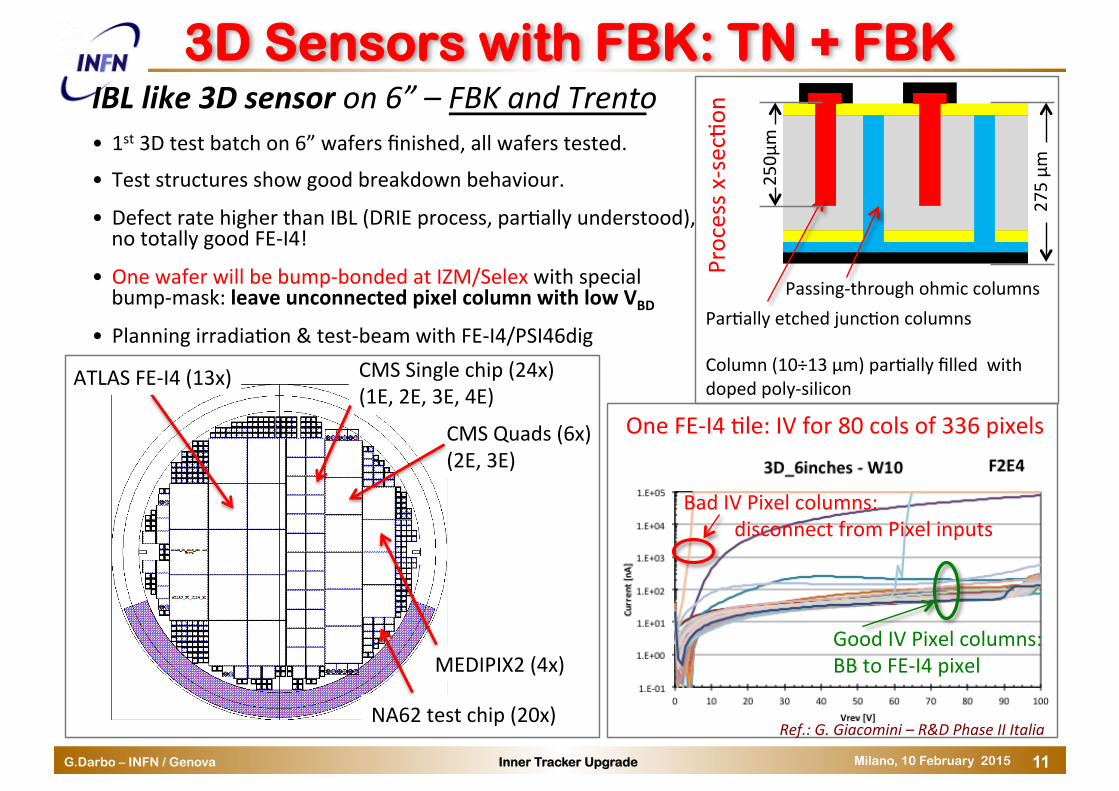
3D Sensors with FBK: TN + FBK IBL like 3D sensor on 6” – FBK and Trento • 1st 3D test batch on 6” wafers finished, all wafers tested. • Test structures show good breakdown behaviour. • Defect rate higher than IBL (DRIE process, par/ally understood), no totally good FE-‐I4!
• One wafer will be bump-‐bonded at IZM/Selex with special bump-‐mask: leave unconnected pixel column with low VBD
• Planning irradia/on & test-‐beam with FE-‐I4/PSI46dig
ATLAS FE-‐I4 (13x) CMS Single chip (24x) (1E, 2E, 3E, 4E)
CMS Quads (6x) (2E, 3E)
MEDIPIX2 (4x)
NA62 test chip (20x)
275 µm
Par/ally etched junc/on columns Column (10÷13 µm) par/ally filled with doped poly-‐silicon
Passing-‐through ohmic columns
250µ
m
Good IV Pixel columns: BB to FE-‐I4 pixel
Bad IV Pixel columns: disconnect from Pixel inputs
One FE-‐I4 /le: IV for 80 cols of 336 pixels
Ref.: G. Giacomini – R&D Phase II Italia Process x
-‐sec/o
n
Inner Tracker Upgrade G.Darbo – INFN / Genova Milano, 10 February 2015 12
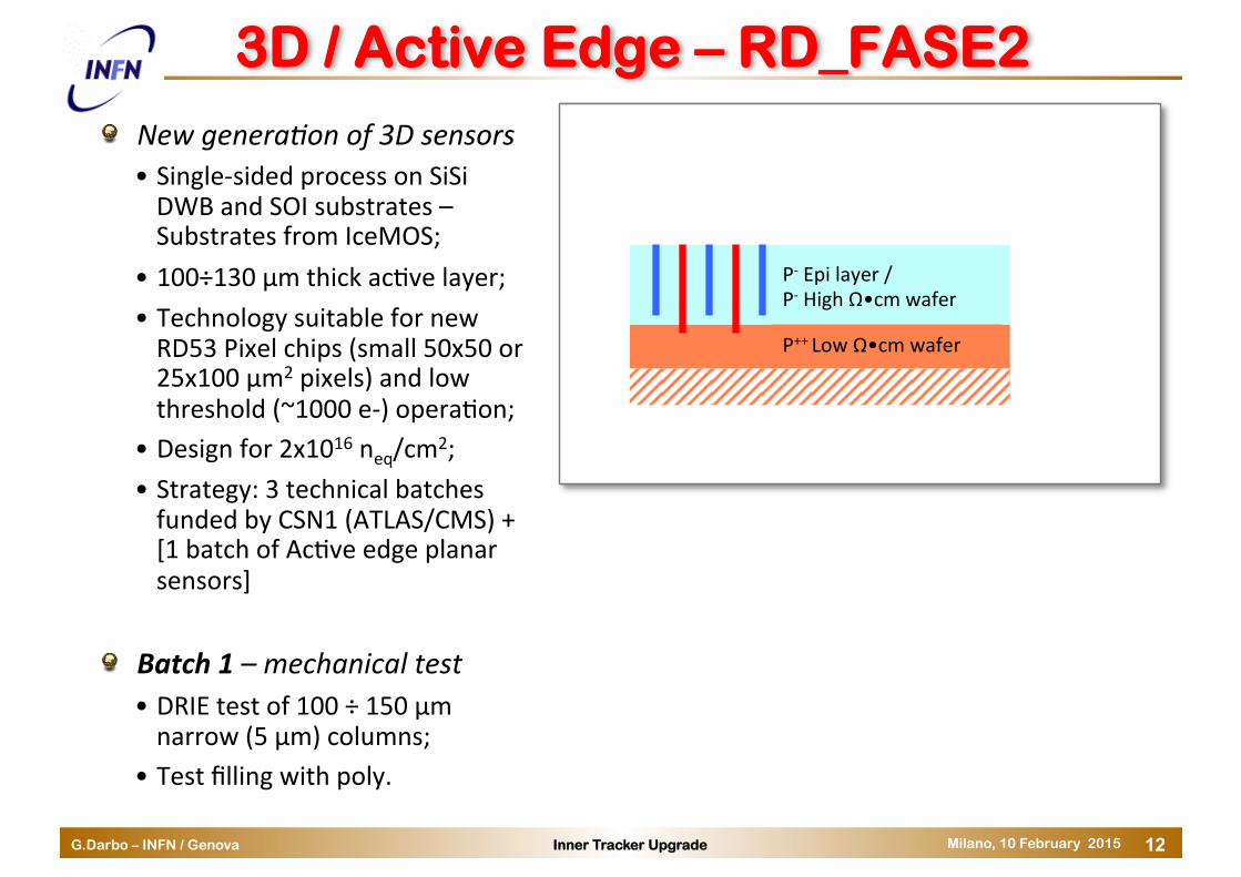
3D / Active Edge – RD_FASE2 New genera6on of 3D sensors • Single-‐sided process on SiSi DWB and SOI substrates – Substrates from IceMOS;
• 100÷130 µm thick ac/ve layer; • Technology suitable for new RD53 Pixel chips (small 50x50 or 25x100 µm2 pixels) and low threshold (~1000 e-‐) opera/on;
• Design for 2x10¹⁶ neq/cm2; • Strategy: 3 technical batches funded by CSN1 (ATLAS/CMS) + [1 batch of Ac/ve edge planar sensors]
Batch 1 – mechanical test • DRIE test of 100 ÷ 150 µm narrow (5 µm) columns;
• Test filling with poly.
P-‐ Epi layer / P-‐ High Ω•cm wafer
P++ Low Ω•cm wafer
-‐Vb
Charge Amp. Bump-‐bond
metal
Thin-‐down
Single side 3D process
p++ col
n++ col
SOI – SiSi D
WB
158 um
5.6 um
3.8 um
Ref.: M. Boscardin and S. Ronchin, FBK
100÷130µm Opt.: 200 nm oxide (SOI)
DRIE for ohmic columns

Inner Tracker Upgrade G.Darbo – INFN / Genova Milano, 10 February 2015 13
ATLAS - FEI4
F10N F10S
F5N F5S
F3N F3S
F2N F2S
FA5S1
FA5S2
Sensor name GRs PT
F10N 10 New
F10S 10 Standard
F5N 5 New
F5S 5 Standard
F3N 3 New
F3S 3 Standard
F2N 2 New
F2S 2 Standard
FA5S1FA5S2 5 Standard
3D / Active Edge – RD_FASE2 Batch 2 – substrates test: planar devices • p-‐type SiSi DWB wafers from IceMOS • 100 ÷ 130 µm high-‐R ac/ve sensor thickness • p-‐spray & p-‐stop isola/on • Started in Sept. 2014, completed in Nov. 2014 • Good electrical characteris/cs – from CV measurements deple/on is in accordance with nominal thickness of ac/ve (device) substrate.
Module assembly: • 5 wafers will be processed by IZM: § Substrate thinning § Metallisa/on with mask of back § BCB processing for HV isola/on
• 1 wafer bump-‐bonded by Selex
Table: good 6les per wafers: • ATLAS (1) – Current limit 0.2 µA, VBD ≥ 100V • CMS (2) – Current limit 50 nA, VBD ≥ 100V
CMS ATLAS
wafer # material thickness p-spray ATLAS (1)
CMS (2)
30 Si-Si 100 2.00E+12 9 / 10 20 / 3033 Si-Si 100 2.00E+12 8 / 10 17 / 3049 Si-Si 100 2.00E+12 8 / 10 20 / 3063 Si-Si 130 2.50E+12 7 / 10 25 / 3069 Si-Si 130 2.50E+12 10 / 10 26 / 3074 Si-Si 130 2.00E+12 8 / 10 19 / 3075 Si-Si 130 2.00E+12 7 / 10 14 / 3080 Si-Si 130 1.50E+12 10 / 10 26 / 3081 Si-Si 130 1.50E+12 8 / 10 26 / 301 FZ 275 2.00E+12
FE-‐I4
Inner Tracker Upgrade G.Darbo – INFN / Genova Milano, 10 February 2015 14
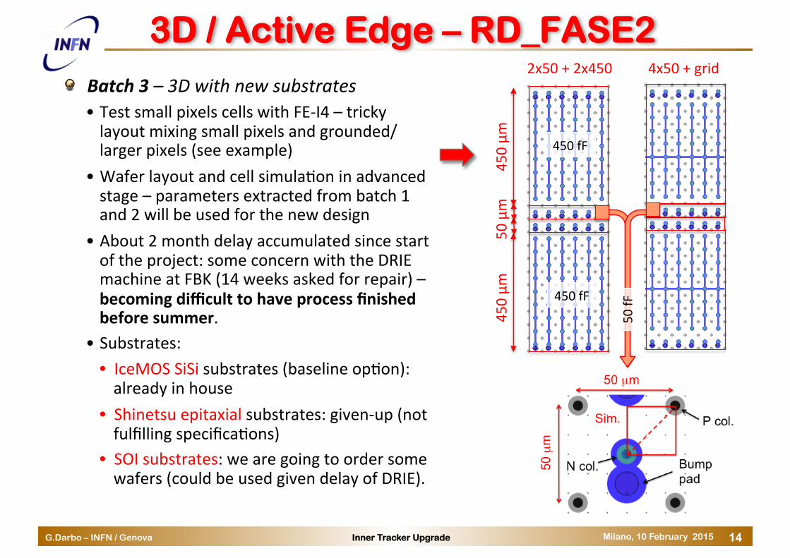
3D / Active Edge – RD_FASE2 Batch 3 – 3D with new substrates • Test small pixels cells with FE-‐I4 – tricky layout mixing small pixels and grounded/larger pixels (see example)
• Wafer layout and cell simula/on in advanced stage – parameters extracted from batch 1 and 2 will be used for the new design
• About 2 month delay accumulated since start of the project: some concern with the DRIE machine at FBK (14 weeks asked for repair) – becoming difficult to have process finished before summer.
• Substrates: • IceMOS SiSi substrates (baseline op/on): already in house
• Shinetsu epitaxial substrates: given-‐up (not fulfilling specifica/ons)
• SOI substrates: we are going to order some wafers (could be used given delay of DRIE).
2x50 + 2x450 4x50 + grid
50 µm
450 µm
450 µm
450 fF
450 fF
50 fF

Inner Tracker Upgrade G.Darbo – INFN / Genova Milano, 10 February 2015 15
Thinking Towards ITk Modules Assume ITk layer 1 & 2 with 3D • Need 3000 RD53 chips/single /le sensors to cover the ~1 m2 area. • Considering 25 /les/wafer (6”), 50 % yield in sensors and 50 % in good /les to used modules: 600 wafers are needed
• FBK + CNM (maybe SINTEF) are in the business – pre-‐produc/on + produc/on from 2018 to 2021.
• Requested exercise: evaluate feasibility and cost!
Considera6ons on bump-‐bonding • Complete qualifica/on at Selex with 6” sensor wafers, FE-‐I4 like modules; • Discuss with Selex plans for R&D and involvement in ITk produc:on: § R&D/Upgrade needs at Selex: qualify process for 120k bumps/chip, upgrade to 12” wafers (RD53 wafers).
§ Consider 8.2 m2 of hybrid pixels → is Selex interested in part of it? • Direct playing with FBK and Selex make easier op/miza/on of BB for 3D sensor and “sell” the full package to the collabora/on.

Inner Tracker Upgrade G.Darbo – INFN / Genova Milano, 10 February 2015 16
Steering R/O R&D Activities Table-‐top ROD/BOC version (BO) • Use exper/se on IBL ROD, no VME needs • Full SW/FW compa/bility with PIT cards • Half ROD, up to 16 FE • Funded by CSN1
Possible ac6vi6es on read-‐out • Expand exis/ng FE-‐I4 R/O systems to HV/HR-‐CMOS (see boXom fig.)
• Common HW/FW/SW interface defini/on • Integrate mini-‐DCS in the read-‐out • GBT concentrator
FE
Generic R/O system USBPix RCE
ROD/BOC PCIExpress
FPGA LV
CTRL TX
RX Mod TX/RX
Ref.: P. MoreZni – R&D Phase II Italia – 23/1/2015
Inner Tracker Upgrade G.Darbo – INFN / Genova Milano, 10 February 2015 17
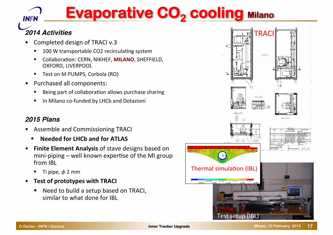
Evaporative CO2 cooling Milano 2014 Activities• Completed design of TRACI v.3
§ 100 W transportable CO2 recircula/ng system § Collabora/on: CERN, NIKHEF, MILANO, SHEFFIELD,
OXFORD, LIVERPOOL § Test on M PUMPS, Corbola (RO)
• Purchased all components: § Being part of collabora/on allows purchase sharing § In Milano co-‐funded by LHCb and Dotazioni
2015 Plans• Assemble and Commissioning TRACI § Needed for LHCb and for ATLAS
• Finite Element Analysis of stave designs based on mini-‐piping – well known exper/se of the MI group from IBL § Ti pipe, 𝜙 2 mm
• Test of prototypes with TRACI § Need to build a setup based on TRACI,
similar to what done for IBL
17
TRACI
Thermal simula/on (IBL)
Test setup (IBL)

Inner Tracker Upgrade G.Darbo – INFN / Genova Milano, 10 February 2015 18
HVR_CCPD Activities on HV/HR-CMOS in CSN5 – BO, GE, MI

Inner Tracker Upgrade G.Darbo – INFN / Genova Milano, 10 February 2015 19
HV / HR – CMOS Pixels in ATLAS ATLAS has strong interest to use HV (High Voltage) CMOS technology on HR (High Resis6vity) substrates as pixel detectors with integrated electronics: • HV: several tens of volt can be applied as bias • HR: the detector can be depleted – charge collec/on happens by dri_ and not diffusion – detector is fast and rad-‐hard
• Thin pixel (high resolu/on) and (must be) small. • Limit of technology: complex R/O not possible → Charge Coupled Pixel Detector (CCPD)
Demonstrator of ~1 cm2
• Significant silicon size on different technologies
• Common interface: easy test • Chip available in the Fall
Thin FE chip
Dielectric (glue)
HV/HR-‐CMOS Amp/Disc layer
Dri_ layer

Inner Tracker Upgrade G.Darbo – INFN / Genova Milano, 10 February 2015 20
STMicroelectronics Chip • NDA Signed with STM
• STM design kit (PDK) + Cadence so_ware available at GE and MI
• Technology evaluaFon: • received 10 transistor arrays from STM: to be used for characteriza/on of radia/on hardness
• Small chip (1 x 2 mm2) submiXed to STM (back in Apr) test pixel sensor and amplifier performance
• Start design of 25 mm2 chip • need to define which of demonstrator features can be implemented.
Layout of the STM test chip 22 I/O and VDD/GND pads 8 pixels (50 x 250 µm2): Collec6ng diode + Amp. Designed by: Ø H. Shrimali and V. Liberali (MI)

Inner Tracker Upgrade G.Darbo – INFN / Genova Milano, 10 February 2015 21
HV/HR-CMOS in Genova Hybridization of CCPD
• Precise gluing with uniform glue thickness of FE-I4 to HV-CMOS chips
• Two samples assembled and used on test beam.
Available setup for testing• USBPix + GPAC + adapter with chip • IR laser (1064 nm) for TCT
measurements
Adapter Board GPAC USBpix
R/O CHIP
R/O CHIP
Spin SU-‐8 photoresist PaXern pillars by mask
Glue deposi/on
R/O CHIP DETECTOR CHIP Align & pressure

Inner Tracker Upgrade G.Darbo – INFN / Genova Milano, 10 February 2015 22
sd
Scan 1
Scan 2
Scan 3
Scan 4
Scan 5
Side A [µm]
Side B [µm]
Scan 1 254.40 257.04
Scan 2 257.31 257.91
Scan 3 256.77 257.83
Scan 4 256.55 257.55
Scan 5 255.97 257.23
Side A
Side B
Credits: A. Rovani & V. Ceriale (GE)

Inner Tracker Upgrade G.Darbo – INFN / Genova Milano, 10 February 2015 23
AIDA-2020 : Funded ! AIDA-‐2020 Funded ! • AIDA-‐2020 has been officially selected by the EC with a funding of 10 M€.
The project has a ranking of 14.5/15 with • 5/5 excellence • 5/5 impact • 4.5 implementa/on
The grant agreement procedure is quite fast
Groups in ATLAS who have been funded: • Genova • Milano • Trento
European Commission - Research - Participants Proposal Submission Forms
Page 1 of 125 Last saved 02/09/2014 at 17:46H2020-CP.pdf - Ver1.88 20140729
Horizon 2020Call: H2020-INFRAIA-2014-2015
Topic: INFRAIA-1-2014-2015Type of action: RIA
Proposal number: 654168
Proposal acronym: AIDA-2020
Table of contents
Section Title Action
1 General information
2 Participants & contacts
3 Budget
4 Ethics
5 Call-specific questions
How to fill in the formsThe administrative forms must be filled in for each proposal using the templates available in the submission system. Some data fields in the administrative forms are pre-filled based on the previous steps in the submission wizard.
This proposal version was submitted by Laurent Serin on 02/09/2014 12:04:24 CET. Issued by the Participant Portal Submission Service.
INFRAIA-1-2014-2015 AIDA-2020
WP1-MGT Project management and coordination
WP2-NA1 Innovation and outreach
WP13-JRA1Innovative gas
detectors
WP14-JRA2Infrastructure for
advanced calorimeters
WP15-JRA3Upgrade of beam and
irradiation test infrastructure
WP10-TA1Beam test facilities
WP12-TA3Detector
characterisation facilities
WP11-TA2Irradiation test
facilities
WP3-NA2Advanced software
WP7-NA6Advanced hybrid pixel detectors
WP4-NA3Microelectronics and
interconnections
WP6-NA5Novel high voltage and resistive CMOS sensors
WP8-NA7Large scale cryogenic liquid
detector
WP5-NA4Data acquisition system for
beam tests
WP9-NA8New support structures and
micro-channel cooling
Transnational Access
Networking
Joint Research
Figure 3.1: Work Package structure and interactions (Pert chart)
25

Inner Tracker Upgrade G.Darbo – INFN / Genova Milano, 10 February 2015 24
Conclusions
ITk project moving ahead: • Kick-‐off mee/ng, Ins/tute Board, … • Scoping scenarios under study • ITk Layout TF
RD_FASE2 • Ac/vi/es on sensors/modules progressing… construc/ve ac/vity with CMS
HVR_CCPD • Test chip submiXed with STM • Hybridiza/on work progressing, few devices assembled at Genova tested in TB
AIDA2020 • Project approved, new resources and R&D framework for HL-‐LHC developments

Inner Tracker Upgrade G.Darbo – INFN / Genova Milano, 10 February 2015 25
SPARE SLIDES

Inner Tracker Upgrade G.Darbo – INFN / Genova Milano, 10 February 2015 26
Activities in ITk ITk management looking at interest of Countries in ITk R&D’s
Table from discussion with Paolo. Comments?
For discussion
Italy& Bologna& PIX&PIX&PIX&
HV/HR&CMOS&sensors&Off/detector&DAQ&Simulation&
Genoa& PIX&PIX&PIX&PIX&PIX&PIX&PIX&
3D&sensor&development&HV/HR&CMOS&sensors&Hybridization&Module&development,&construction&and&testing&Local/Global&support&design&Off/detector&DAQ&Simulation&
Cosenza& PIX&PIX&
3D&sensor&development&Simulation&
Lecce& PIX& Simulation&Milan& PIX&
PIX&PIX&PIX&PIX&PIX&PIX&PIX&COM&
HV/HR&CMOS&sensors&3D&sensor&development&RD53&Hybridization&Module&development&and&testing&Local/Global&support&design&and&production&Off/detector&electronics&(LV&power&supplies)&Simulation&Off/line&software&
Udine& PIX&PIX&PIX&
3D&sensor&development&Module&development&and&testing&On/line&monitoring&
Trento& PIX&PIX&PIX&
3D&sensor&development&HV/HR&CMOS&sensors&Module&development&and&testing&
&

Inner Tracker Upgrade G.Darbo – INFN / Genova Milano, 10 February 2015 27
FTE 2015 on ATLAS Related R&D Total 13.8 FTE for the 3 R&D of interest of ITk.
Sezione First+Name Family+Name RuoloBO Davide Falchieri Tecn.Cat.DBO Alessandro Gabrielli RICBO Matteo Negrini RICBO Carla Sbarra RICBO Antonio Sidoti RICBO Maximiliano Sioli PABO Mauro Villa PA
RD_FASE2 HVR_CCPD CHIPIX650.20EEEEEEEEEEEE FEEEEEEEEEEEEEE FEEEEEEEEEEEEEE0.20EEEEEEEEEEEE 0.10EEEEEEEEEEEE FEEEEEEEEEEEEEE0.20EEEEEEEEEEEE FEEEEEEEEEEEEEE FEEEEEEEEEEEEEEFEEEEEEEEEEEEEE 0.20EEEEEEEEEEEE FEEEEEEEEEEEEEE0.20EEEEEEEEEEEE FEEEEEEEEEEEEEE FEEEEEEEEEEEEEE0.20EEEEEEEEEEEE FEEEEEEEEEEEEEE FEEEEEEEEEEEEEEFEEEEEEEEEEEEEE 0.10EEEEEEEEEEEE FEEEEEEEEEEEEEE
CS Anna MastroberardinoRUECS AntonioE Policicchio AssegnistaECS Daniela Salvatore AssegnistaEGE Michele Biasotti AssegnistaEGE Valentina Ceriale Dott.EGE Giovanni Darbo DR
0.30EEEEEEEEEEEE FEEEEEEEEEEEEEE FEEEEEEEEEEEEEE0.30EEEEEEEEEEEE FEEEEEEEEEEEEEE FEEEEEEEEEEEEEE0.30EEEEEEEEEEEE FEEEEEEEEEEEEEE FEEEEEEEEEEEEEEFEEEEEEEEEEEEEE 0.10EEEEEEEEEEEE FEEEEEEEEEEEEEEFEEEEEEEEEEEEEE 0.20EEEEEEEEEEEE FEEEEEEEEEEEEEE0.55EEEEEEEEEEEE 0.30EEEEEEEEEEEE FEEEEEEEEEEEEEE
GE Andrea Gaudiello Dott.EGE Claudia Gemme RICGE Elisa Guido AssegnistaEGE Paolo Morettini 1FRICGE Leonardo Rossi DRGE Mario Sannino PAMI Gianluca Alimonti RICMI Attilio Andreazza PA
0.30EEEEEEEEEEEE 0.30EEEEEEEEEEEE FEEEEEEEEEEEEEE0.30EEEEEEEEEEEE 0.10EEEEEEEEEEEE FEEEEEEEEEEEEEE0.10EEEEEEEEEEEE FEEEEEEEEEEEEEE FEEEEEEEEEEEEEE0.60EEEEEEEEEEEE 0.20EEEEEEEEEEEE FEEEEEEEEEEEEEEFEEEEEEEEEEEEEE 0.20EEEEEEEEEEEE FEEEEEEEEEEEEEE0.30EEEEEEEEEEEE 0.20EEEEEEEEEEEE FEEEEEEEEEEEEEE0.50EEEEEEEEEEEE FEEEEEEEEEEEEEE FEEEEEEEEEEEEEEFEEEEEEEEEEEEEE 0.30EEEEEEEEEEEE FEEEEEEEEEEEEEE
MI Mauro Citterio DTECMI Simone Coelli TEC
FEEEEEEEEEEEEEE 0.15EEEEEEEEEEEE FEEEEEEEEEEEEEE0.30EEEEEEEEEEEE FEEEEEEEEEEEEEE FEEEEEEEEEEEEEE
MI Valentino Liberali PAMI Chiara Meroni DRMI Francesco Ragusa POMI Shojaii Seyedruhollah Dott.EMI Hitesh Shrimali AssegnistaEMI Alberto Stabile AssegnistaEMI Clara Troncon 1FRICTN GianFFranco DallaEBettaE PAE
FEEEEEEEEEEEEEE 0.20EEEEEEEEEEEE 0.40EEEEEEEEEEEE0.20EEEEEEEEEEEE 0.30EEEEEEEEEEEE FEEEEEEEEEEEEEE0.20EEEEEEEEEEEE 0.30EEEEEEEEEEEE FEEEEEEEEEEEEEEFEEEEEEEEEEEEEE FEEEEEEEEEEEEEE 0.30EEEEEEEEEEEEFEEEEEEEEEEEEEE 0.50EEEEEEEEEEEE FEEEEEEEEEEEEEEFEEEEEEEEEEEEEE 0.30EEEEEEEEEEEE 0.30EEEEEEEEEEEE0.20EEEEEEEEEEEE FEEEEEEEEEEEEEE FEEEEEEEEEEEEEE0.40EEEEEEEEEEEE FEEEEEEEEEEEEEE FEEEEEEEEEEEEEE
TN David Macii Dott.ETN Roberto Mendicino Dott.ETN DMS Sultan Dott.ETN GiovanniE Verzellesi POEUD Marina Cobal PA
0.50EEEEEEEEEEEE FEEEEEEEEEEEEEE FEEEEEEEEEEEEEE0.50EEEEEEEEEEEE FEEEEEEEEEEEEEE FEEEEEEEEEEEEEE1.00EEEEEEEEEEEE FEEEEEEEEEEEEEE FEEEEEEEEEEEEEE0.40EEEEEEEEEEEE FEEEEEEEEEEEEEE FEEEEEEEEEEEEEE0.20EEEEEEEEEEEE FEEEEEEEEEEEEEE FEEEEEEEEEEEEEE
UD MarioEPaolo Giordani RUETotal 37 Total
0.30EEEEEEEEEEEE FEEEEEEEEEEEEEE FEEEEEEEEEEEEEE8.75 4.05 1
Sezione RD_FASE2 HVR_CCPD CHIPIX65BO 1.00&&&&&&&&&&&& 0.40&&&&&&&&&&&& (&&&&&&&&&&&&&&CS 0.90&&&&&&&&&&&& (&&&&&&&&&&&&&& (&&&&&&&&&&&&&&GE 2.15&&&&&&&&&&&& 1.60&&&&&&&&&&&& (&&&&&&&&&&&&&&MI 1.40&&&&&&&&&&&& 2.05&&&&&&&&&&&& 1.00&&&&&&&&&&&&TN 2.80&&&&&&&&&&&& (&&&&&&&&&&&&&& (&&&&&&&&&&&&&&UD 0.50&&&&&&&&&&&& (&&&&&&&&&&&&&& (&&&&&&&&&&&&&&Totale 8.75======== 4.05======== 1.00========
Prev=2015

Inner Tracker Upgrade G.Darbo – INFN / Genova Milano, 10 February 2015 28
RD_FASE2 – “Richieste 2015”
Legend: ATLAS Common ATLAS / CMS
Akvità Descrizione BO CS GE MI TN UD
3D
6" Wafer procurement (SOI, wafer bonding, epi) -‐ -‐ -‐ -‐ 10.0 -‐ PicoScope 6407 Digi/zer with 1.5 GHz probes and accessories. -‐ -‐ -‐ -‐ 8.5 -‐
BB
6" dummy wafers -‐ test deposi/on on 6" and high-‐density bumps (150 k-‐bumps/chip) -‐ -‐ -‐ 20.0 -‐ -‐
BB for 3D sensor test -‐ -‐ 24.0 -‐ -‐ -‐
MOD Upgarde R/O Systems -‐ 2.0 2.0 2.0 -‐ 2.0
Module assembly and irradia/on, RD on flex -‐ -‐ 10.0 -‐ -‐ -‐
MM-‐R/O Mul/ module R/O 15.0 -‐ -‐ -‐ -‐ -‐
CO2/µCH Develop µ-‐channel cooling -‐ -‐ -‐ 10.0 -‐ -‐
Total requested by ATLAS 15.0 2.0 36.0 32.0 18.5 2.0
105.5
Trento: • Request of 4 k€ of Travel Money
for test-beam participation and support.