Numerical modelling of nanoparticle deposition in the nasal cavity and the tracheobronchial airway

Ink Jet Deposition of Inorganic Nanoparticle
Materials as a Route to Desktop Fabrication of
Integrated Logic and Micromachinery
by
Sawyer Buckminster Fuller ARCHIVES
Submitted to the Department of Mechanical Engineeringin partial fulfillment of the requirements for the degree of
Bachelor of Science in Mechanical Engineering
at the
MASSACHUSETTS INSTITUTE OF TECHNOLOGY
June 2000
© Massachusetts Institute of Technology 2000. All rights reserved.
H1
Author ...............Department of Mechanical Engineering
May 5, 2000
Certified by......Joseph Jacobson
Associate ProfessorThesis Supervisor
A ccepted by .......................................................Ernest C. Cravalho
Chairman, Undergraduate Thesis Comittee
i ' V

Ink Jet Deposition of Inorganic Nanoparticle Materials as a
Route to Desktop Fabrication of Integrated Logic and
Micrormachinery
by
Sawyer Buckminster Fuller
Submitted to the Department of Mechanical Engineeringon May 5, 2000, in partial fulfillment of the
requirements for the degree ofBachelor of Science in Mechanical Engineering
Abstract
In this thesis, ink jet printing is investigated as a means to fabricate sub-millimeterelectrical and mechanical systems such as micro-actuators and integrated circuits.Nano-crytalline atom cluster dispersions in a solvent-based dispersant are used as
the primary building material, the first known ink jet application of such material to
build microelectromechanical structure. The nanoparticle ink offers a means to addi-
tively build devices out of inorganic materials with material properties far superior to
organic materials and comparable to what is normally created in a vacuum. Demon-strated devices include an electrostatic linear drive motor, a 1-bit radiofrequency(RF) remote sensable tag, in-plane and out-of-plane electrothermal actuators, and acapacitor. All processes conducted were in an open atmosphere at plastic-compatibletemperatures, suggesting a potential route to a desktop fab.
Thesis Supervisor: Joseph JacobsonTitle: Associate Professor

Acknowledgments
I'll start off by thanking me, for enduring all this work, which often has entailed long
unpleasant episodes. I'm hoping my future me will be glad I did. I want to thank my
mother, Patrice Engle, and all of my grandparents, Pearl and Mel Fuller and Murry
and Ernest Lauser, for funding my undergraduate education and that wisdom-like
insight into life, even when it looked like I was never going to graduate. Thanks to
Babak Nivi who invited me to work at the Media Lab, to Colyn and Eric for providing
me healthy competition for good results (and a minimum of espionage and sabotage),
to Brian for the AFM imaging, to Joe for being the model of a good leader and for
letting me take on my own project, to Leila for when she helped remind me once
upon a time why life and school were worth working for, to Dad, Kirk Fuller, for the
love of invention, spirit, and hard work, to Henry for the global perspective and for
being my step dad, to Saul for the hotplate, to Jeremy Levitan for MEMS insight
and help, to a lot of incredible people, some of which I have even yet to meet, and to
the times when I've gotten to experience the happiness, warmth, and love of life.
I can't wait to graduate.
This work was funded under the Defense Advanced Research Project Agency
contract DABT63-99-C-0033 and the Media Laboratory's Things That Think con-
sortium.
3

Contents
1 Introduction
2 Background
2.1 Ink Jet Fabrication . . . . . . . . . . . .
2.1.1 Overview . . . . . . . . . . . . .
2.1.2 A history of ink jet . . . . . . . .
2.1.3 New uses . . . . . . . . . . . . .
2.2 Nanoparticles as Building Materials . . .
2.3 Comparison with Vacuum Deposition . .
2.4 D evices . . . . . . . . . . . . . . . . . .
2.4.1 Linear drive motor . . . . . . . .
2.4.2 Radiofrequency identification tag
2.4.3 Electrothermal actuator . . . . .
3 Methods
3.1 Ink Jet Printing Machine . . . . . . . . . . . . . . . . . . .
3.1.1 Ink jet system . . . . . . . . . . . . . . . . . . . . .
3.2 Nanoparticle Ink . . . . . . . . . . . . . . . . . . . . . . .
3.3 Substrate . . . . . . . . . . . . . . . . . . . . . . . . . . .
3.4 Printing properties and optimizations . . . . . . . . . . . .
3.4.1 Wet ink pattern instability . . . . . . . . . . . . . .
3.4.2 Improvements resulting from heating the susbtrate
4 Results
4
8
10
. . . . . . . . . . . . . . . . 1 0
. . . . . . . . . . . . . . . . 1 0
. . . . . . . . . . . . . . . . 1 1
. . . . . . . . . . . . . . . . 1 1
. . . . . . . . . . . . . . . . 1 2
. . . . . . . . . . . . . . . . 1 4
. . . . . . . . . . . . . . . . 1 4
. . . . . . . . . . . . . . . . 1 4
. . . . . . . . . . . . . . . . 1 4
. . . . . . . . . . . . . . . . 1 5
17
. . . . . . 17
. . . . . . 18
. . . . . . 20
. . . . . . 21
. . . . . . 21
. . . . . . 22
. . . . . . 22
23
4.1 Droplet specifics . . . . . . . . . . . . . . . . . . . . . . . . . . . . . . 23
4.1.1 morphology . . . . . . . . . . . . . . . . . . . . . . . . . . . . 23
4.1.2 Droplet placement repeatability . . . . . . . . . . . . . . . . . 23
4.2 Basic patterning . . . . . . . . . . . . . . . . . . . . . . . . . . . . . . 25
4.3 Linear Motor . . . . . . . . . . . . . . . . . . . . . . . . . . . . . . . 25
4.4 Radiofrequency identification tag . . . . . . . . . . . . . . . . . . . . 26
4.5 Electrothermal actuators . . . . . . . . . . . . . . . . . . . . . . . . . 28
4.5.1 In-plane actuator . . . . . . . . . . . . . . . . . . . . . . . . . 28
4.5.2 Out-of-plate actuator . . . . . . . . . . . . . . . . . . . . . . . 30
4.6 Capacitor . . . . . . . . . . . . . . . . . . . . . . . . . . . . . . . . . 31
5 Conclusion 32
5.0.1 C ost . . . . . . . . . . . . . . . . . . . . . . . . . . . . . . . . 32
5.0.2 Performance . . . . . . . . . . . . . . . . . . . . . . . . . . . . 33
5.0.3 The limits of size . . . . . . . . . . . . . . . . . . . . . . . . . 33
5.1 Applications . . . . . . . . . . . . . . . . . . . . . . . . . . . . . . . . 33
A Program for Printing Planar Electrothermal Actuator 35
5

List of Figures
2-1 TEM image of sintered cadmium selenide nanoparticle film. Each vis-
ible grain is a 2.5 nm nanoparticle. Source: Brent Ridley. . . . . . . . 13
2-2 A standard for comparison: vacuum-deposited silicon microelectrome-
chanical actuator. Source: Jeremy Levitan. . . . . . . . . . . . . . . . 16
3-1 The gantry system used to position the ink jet print head. . . . . . . 18
3-2 Comparison of the basic forms of small-scale ink jet. The three types
are piezo, thermal, and continuous jet, respectively. . . . . . . . . . . 19
3-3 A layer of individual silver ink droplets, each about 80 pm in diameter. 22
4-1 The disc of a single droplet of nanoparticle silver ink imaged with
atomic force microscope. The images, starting at the top, are a per-
spective view, overhead vew, and a cross. The vertical dimension is
multiplied by a factor of 80 in the perspective view. . . . . . . . . . . 24
4-2 Ink jet printed pattern for a 7-segment display driver for E-ink. . . . 25
4-3 Ink jet printed linear drive motor printed on polyimide film. Figure
show n to scale. . . . . . . . . . . . . . . . . . . . . . . . . . . . . . . 26
4-4 A series of stills taken from a movie of linear motor operation. .... 26
4-5 Ink jet printed 1-bit radiofrequency identification tag. . . . . . . . . . 27
4-6 A radiofrequency spectrum analyzer detecting the 25 MHz resonant
absorption frequency of the printed tag . . . . . . . . . . . . . . . . . 27
4-7 Fabrication process for ink jet printed planar actuator: (A) Deposit of
sacrificial release material. (B) Draw-down. (C) Nanoparticle ink jet
deposit and cure. (D) Removal of sacrificial release layer. . . . . . . 29
6

4-8 Ink jet printed planar electrothermal actuator. . . . . . . . . . . . . . 29
4-9 Alternate view of ink jet printed planar actuator. . . . . . . . . . . . 30
4-10 Out-of-plane electrothermal actuator. . . . . . . . . . . . . . . . . . . 30
5-1 Ink droplet at 4000 dpi generated from a splash demonstrates feature
size comparable to those attained by lithography. . . . . . . . . . . . 34
7

Chapter 1
Introduction
The suggestion that launched this body of work was that ink jet printing could be used
as an alternate approach to fabricating sub-millimeter scale systems such as integrated
circuits and micromachinery. While vacuum metal vapor deposition/lithograph/etch
systems are presently used for both applications to reasonable success, the process
is very expensive and turn-around time can take months. An all-additive printing
process such as ink jet whose deposition materials were of comparable quality could
substantially alter the means by which such devices are traditionally fabricated.
The benefits of ink jet are substantially summarized in that the process is fairly
easy compared to vacuum deposition/etch: it is additive, data-driven instead of mas-
ter driven, flexible in terms of materials, and low temperature. Other routes for
exploration include its ability to deposit onto nonplanar substrates and its ability to
build three dimensional structure.
In basic form, an ink jet print head is a machine that ejects single droplets of
liquid on command. The printhead is moved over the substrate, depositing droplets
of functional "ink" to build a multilayer devices. The range of materials that can be
deposited is only limited to the subet that can be suspended in liquid. Where the
results of this work differ from previous work is in the use of nanoparticle-based inks.
Nanoparticles, typically consisting of 10's to 1000's of atoms, are minute particles
of metal, semiconductor, or insulator whose morphology causes them to have a sub-
stantially reduced melting point compared to bulk material. Though ink jet printing
8

metals has traditionally required elaborate measures, printing nanoparticles by ink
jet is comparatively easy. This is a result of their dispersability in liquid. With the
state of the art in commercial ink jet printers at a roughly 20 pm feature size, the
possibility exists for ink jet to print circuitry, logic, and even micromachines of high
resolution.
The goal of this project is to demonstrate the ability of ink jet printed, nanoparticle-
based inks to yield electrically and mechanically functional devices with performance
characteristics high enough to make the process comparable to devices normally cre-
ated in a vacuum. Chapter 2 describes the ink jet process and previous work with ink
jet to build devices. More details about nanoparticles are given, as well as other work
with nanoparticles that could be used with ink jet. The use and physical description
devices reported in this work are also included. These include an electrostatic linear
drive motor, a radiofrequency ID tag, an electrothermal actuator, and a capacitor. In
Chapter 3, the experimental apparatus and general process used to build the devices
is described. In Chapter 4, the results of the work are presented, including perfor-
mance parameters of the various devices. In Chapter 5, the findings and further work
are summarized. Included in the appedices are a listing of the control code to build
various structures.
9

Chapter 2
Background
2.1 Ink Jet Fabrication
2.1.1 Overview
The form of ink jet suggests its use as a means to pattern arbitrary materials onto
a substrate in planar layers. A specially designed ink jet head ejects tiny droplets of
liquid one at a time onto a substrate in response to an electrical signal. It is moved
over the substrate so that a pattern of material is left. As each droplet is deposited,
the liquid portion of the ink evaporates, leaving behind a disc of the non-evaporating
portion of the ink. The discs are deposited layer by layer. The dimensions of the disk
depend on a range of factors including the wettability of the substrate, its porosity,
the density of solids in the ink, the volume of the ink droplet, the speed of its impact,
and the temperature of the substrate.
Because a computer can command the position of each droplet, the process is a
data-driven. In contrast to a non-data-driven process such as lithography, a fully
data-driven process requires no previously-existing information to be incorporated
into fabrication.
10

2.1.2 A history of ink jet
Ink jet has seen commercial application for over thirty years. The first form was of
a form called continuous jet, where individual droplets separated out of a continuous
stream as a result of a phenomenon first studied by Reyleigh and called the Rayleigh
instability. The individual droplets were capacitively charged and then electrostat-
ically deflected, yeilding a pattern on the substrate. Continuous jet printing sees
most of its use in high-throughput commercial graphics applications and in product
marking. More recently, drop-on-demand (DOD) ink jet printing, which makes use of
individual pressure impulses in an ink chamber, has been used in commercial desktop
printers from a range of manufacturers.
2.1.3 New uses
While most of the focus on ink jet has traditionally been devoted to depositing pig-
ments and dyes, more and more attention has been given to the use of ink jet for
non-typographic applications. Expanding from its roots as a print medium, ink jet
has been explored as a means to deposit a range of materials. Its all-additive, data-
driven nature suggests its application to 3-dimensional prototyping. Its reasonably
high resolution suggests applications in electronics fabrication.
Both of applications have seen commercial use. A body of work first proposed in
a thesis by Paul Williams at MIT on 3-dimensional printing[1] launched a company
called Z-corp that specializes in manufacturing printers to build prototype plastic
models. The process involves ejecting a resin binder into select areas of successive
layers of loose powder. Another approach seeing commercial use involves directly jet-
ting the polymer structure. Work on using ink jet to eject solder for ball-grid arrays
for flip-chip semiconductor mounting[2][3] has seen application in the seminconduc-
tor industry. Other work has included horizontal overhang structures built from
wax dropets,[4] displays made from droplets of organic light-emitting diodes[5] and
polymers,[6] printed patterns of photoresists and solid particles,[7] and conductive
traces made from metallo-organic decomposition inks. [8]
11

Trends in ink jet printing point to smaller droplet size, higher droplet rates, and
an increasing material set. The smallest droplet sizes currently attainable can yield
feature sizes as low as 20 pim.[9] To date, however, efforts at using ink jet to print
materials with silicon-like capabilities has been limited by low conductivity and low
mechanical strength. While the resin-powder "three dimensional printing" process
proposed by Williams has been used to build metal-powder prototypes, their feature
size is relatively high. The metallo-organic inks have very low metal concentration.
Organic conductors have fundamental limits to their ability to conduct, and the solder
and other metal-jet systems are in incipient stages and in some cases require extreme
processing conditions. What is needed is a new type of ink material.
2.2 Nanoparticles as Building Materials
Recently, in an article in Science, researchers in my group demonstrated the use
of nanoparticles as the semiconductor in a field effect transistior.The all-inorganic
transistor exhibited the highest mobility for a printed semiconductor material.[10] [11]
Nanoparticles are receiving much interest from the device research community because
of the unique characteristics that arise as a result of their small size. [12]
Nanoparticles are small clusters of metal, semiconductor, or insulator, typically
consisting of 10's to 1000's of atoms. Particle sizes are usually several nanometers
across. In the context of ink jet printing, nanoparticles have two striking features
which make them ideally suited for device fabrication. First, they exhibit a size
dependent melting point depression which has been demonstrated to be as much as
1000*C below the bulk melting point.[13][14] The melting point is reduced as a result
of the relatively large ratio of surface area to volume of the nanoparticles, causing
neighboring particles to tend to fuse at elevated temperatures. My research group
uses the term nanotectic to refer to the size-dependent melting point depression of
the nanoparticle material. The use and arrangement of nanotectic materials to build
functional structure we call nanotectonics. Secondly, nanoparticles are relatively easy
to suspend in a liquid medium because of their small size. Typically a hydrocarbon
12
chain such as a thyol, called a capping group, covers the surface of each nanoparticle
and causes neighboring particles to repel.
The processes for making nanoparticle inks vary from material to material, but
in general it is not very difficult. Typically nanoparticles are made by rapidly mixing
very certain chemicals and then filtering the resultant material to retain a certain size
distribution. An alternate approach involves vaporizing and condensing the precursor
material into solid particles.
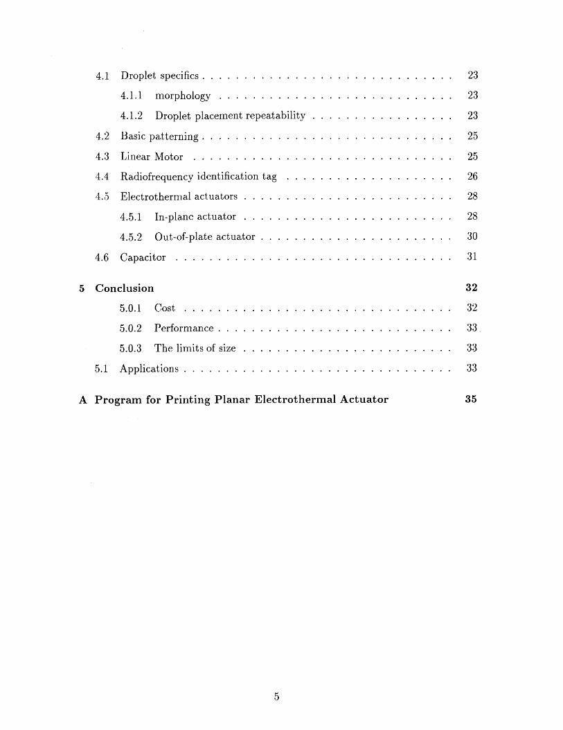
In Figure 2-1, a tunneling electron microscope (TEM) image of a sintered film
of cadmium selenide nanoparticles shows crystal grain structure developing in the
nanoparticle film. The cadmium selenide exhibited the semiconducting field effect
that allowed it to be used in a transistor. [10]
Figure 2-1: TEM image of sintered cadmium selenide nanoparticle film. Each visible
grain is a 2.5 nm nanoparticle. Source: Brent Ridley.
13
2.3 Comparison with Vacuum Deposition
It is proposed that nanoparticle deposition is a cost-effective alternative to vacuum de-
position. The majority of high-resolution and high-quality devices such as transistors
and MEMS are fabricated with vacuum-deposition processes. While most vacuum
deposition processes require a separate pattern and etch process, lithography masks,
and even a vacuum, nanoparticle deposition is characterized by the ease with which
it can be used to build high-quality devices.
2.4 Devices
The choice of device presented in this report was made with a number of factors,
including ease of fabrication, utility, and ability to be easily used with more complex
devices.
2.4.1 Linear drive motor
An operational linear drive motor sugguests an ability to fabricate a disposable pro-
grammable chemistry system. The operation of a linear botor is based on capacitively
charging insulating material and then using its electrostatic charge to move it. Three
repeating interdigitated conducting bus lines are alternately pulsed to high voltage
to charge and then move the medium. An operating linear drive motor is a useful
demonstration of conductivity.
2.4.2 Radiofrequency identification tag
Current radiofrequency identification tags using silicon logic cost about a dollar. A
system for printing single or multiple tags could substantially reduce their cost and
bring them into ubiquity. In basic form, a radio frequency is transmitted to the tag
to establish
1. its presence, and
14
2. its identity.
To detect the presence of the tag requires only that its resonant frequency be
approximately known. The simplest form of RFID tag is an inductor-capacitor circuit
made from a coil of wire. When a radiofrequency signal is transmitted to the coil of
the tag, the tag's presence either attenuates that signal or causes it to remain briefly
after the source has been turned off. Either the attenuation or the transient response
is detectable by the source. This simple form of tag carries one bit of information
which corresponds to its state of presence.
The second form of tag, called a multi-bit tag, requires that the tag return in-
formation about its identity. This can be accomplished by implimenting a logical
finite state machine with control over the resonant properties of the coil. Over time
a series of bits are repeatedly transmitted by changing the inductance or capacitance
of the coil, specifying the unique identity of that tag. Commercial tags of this type
currently cost a dollar or more per tag.
An operational single-bit radiofrequency tag requires a high electrical conductivity
to reach a high resonance Q factor. A detectable printed tag demonstrates high
conductivity. A multibit printed tag requires onboard printed logic.
2.4.3 Electrothermal actuator
An actuator is a basic piece of micromechanical machinery necessary to generate
mechanical motion. One type of actuator, an electrothermal actuator or "heatuator"
uses a special configuration to geometrically amplify thermal expansion. An image
of a vacuum deposited actuator of such a design, a standard for comparison, is in
Figure 2-2. Its minimum feature size is roughly 1 pm. The vertical portion of the
device is mechanically separate from the substrate, and current is passed from the
left contact pad to the right, through the tip of the cantilever. The thinner side
is subjected to a higher electrical current density which causes it to heat further,
expanding. The thermal expansion incites lateral motion at the tip. Such a actuators
were pioneered with vacuum deposition as systems optimized for low voltage and low
15

area.[15][16] Levers, gears, and other machinery can be attached to the end of the
actuator to derive useful work from the actuator.[17]
Figure 2-2: A standard for comparison:chanical actuator. Source: Jeremy Levita.
vacuum-deposited silicon microelectrome-
To build an operational electrothermal actuator of this design requires a building
material of reasonable mechanical strength that is conductive, and the ability to
remove a sacrifical release layer to separate it from the substrate.
16

Chapter 3
Methods
3.1 Ink Jet Printing Machine
The system used to position the ink jet head in 3-space was a linear-motor type
system for industrial application manufactured by Aerotech. With a repeatability
of +2pm, inaccuracy due to the gantry was not a significant factor in device quality.
A specialized form of G-code and a Windows-based interface by Aerotech served as
the means to command the printing process. For simplicity, a single nozzle out of the
48 on the print head was used. A signal generator, amplified by a positive feedback
operational amplifier circuit, was used to provide the pulse signal to drive the nozzle
at a continuous frequency, such as 222 drops per second. Using a logical AND gate, an
output bit controlled by the PC interface was used to command whether the signal
reached the nozzle. To achieve uniform droplet spacing, commands to the gantry
were written to insure that it had fully accelerated before the nozzle was turned on.
The line and dot functions provided by this system constituted a serial, vector-based
manufacturing system. While multiple nozzles and a rastering system could have
been adapted, a serial drawing approach was sufficient for the single devices explored
in this work.
Figure 3-1 is a photograph of the gantry system with ink jet head and fume box
used in this project.
17

Figure 3-1: The gantry system used to position the ink jet print head.
3.1.1 Ink jet system
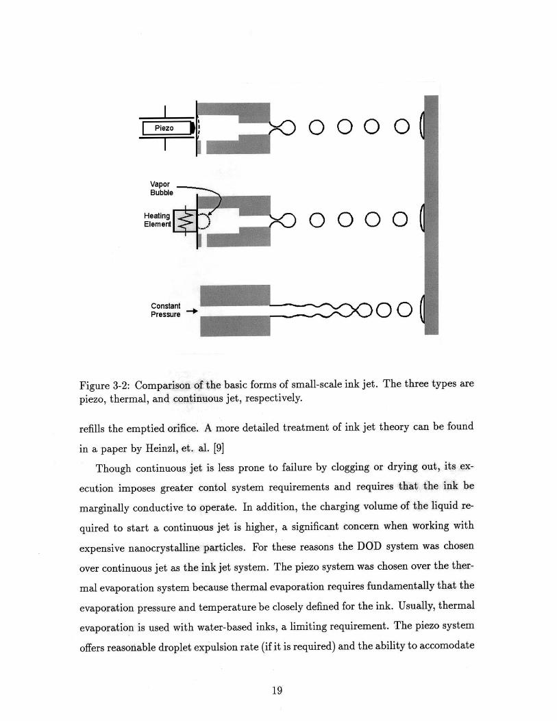
The two basic forms of ink jet printing at the scale described in this report are known
as continuous jet and drop-on-demand (DOD). In each case, a stream of droplets is
expelled from a tiny orifice and lands on a substrate some 1 mm to 100 mm away.
Figure 3-2 pictorially illustrates continuous jet and two forms of DOD. Continuous
jet relies on surface tension instability (called the Rayleigh instability) to break apart
a continuous stream into separate droplets. Usually the droplets are capacitively
charged at the expulsion point and electrostatically deflected to start or stop the flow,
or to position the droplets. DOD, in contrast, involves ejecting individual droplets
on demand by causing a sudden pressure increase in the ink chamber. Typically
the pressure increase is achieved by either thermally evaporating a tiny droplet of
material within the chamber or by deflecting a chamber wall by charging a piezo
crystal. Expulsion is only achieved when the kinetic energy of the ink in the orifice
is higher than the potential energy of the surface tension required to form a droplet.
Once the droplet has been expelled, hydrodynamic pressure waves or capillary action
18
~IPiezo
VaporBubble
HeatingElement
ConstantPressure
0000
~K~0000
00
Figure 3-2: Comparison of the basic forms of small-scale ink jet. The three types are
piezo, thermal, and continuous jet, respectively.
refills the emptied orifice. A more detailed treatment of ink jet theory can be found
in a paper by Heinzl, et. al. [9]
Though continuous jet is less prone to failure by clogging or drying out, its ex-
ecution imposes greater contol system requirements and requires that the ink be
marginally conductive to operate. In addition, the charging volume of the liquid re-
quired to start a continuous jet is higher, a significant concern when working with
expensive nanocrystalline particles. For these reasons the DOD system was chosen
over continuous jet as the ink jet system. The piezo system was chosen over the ther-
mal evaporation system because thermal evaporation requires fundamentally that the
evaporation pressure and temperature be closely defined for the ink. Usually, thermal
evaporation is used with water-based inks, a limiting requirement. The piezo system
offers reasonable droplet expulsion rate (if it is required) and the ability to accomodate
19
a wide range of ink materials, making it a good choice for device fabrication.
A piezo-based ink jet head manufactured by Hitachi Koki was selected for primary
use because of its good solvent immunity, low priming volume, and operating temper-
ature range. The head was a 48-nozzle generation II head originally used in a since
discontinued solid wax desktop printer. The quoted droplet volume ranges from 75
to 150 picoliters, variable by ink viscosity and signal magnitude. Later ink jet heads
developed by the company offer lower droplet volume and increased number of heads,
but for the purposes of this experiment, the head's droplet volume was sufficient.
3.2 Nanoparticle Ink
The conducting material was nanoparticle silver with a particle size of 5-7 nm sus-
pended in a-terpineol and a capping group. The process of fabrication, carried out
by a commercial supplier, involves rapid vaporization of silver. The vapor is allowed
to condense slightly and then is collected in particle form. To suspend it in liquid, the
capping group, believed to be a thyol, is added to the mixture. Nanoparticle silver of
similar quality has been manufactured in-lab. Nanoparticle indium tin-oxide (ITO),
a clear conductor, was also used and found to exhibit conductivity when printed.
The high conductivity of silver and gold led to their use predominantly. Because
high concentration of solid material in a liquid change its properties, the ink jet head
required a low concentration. For this reason, in all results presented, the ink was
composed of 10% by weight nanoparticle material, the rest of which was the capping
group and a-terpineol.
Each ink jet ejected droplet of ink contains millions of nanoparticles. As the
solvent in the ink evaporated, the nanoparticle solution leaves a pasty, purple sub-
stance on the substrate. In this form the nanoparticle material is considered to be
"green." The green material iss solid enough that successive layers can be added on
top if desired without disrupting the underlying pattern. Once the entire structure
is deposited, the device is heated and the nanoparticles are heated and caused to
melt together in a process called sintering. Sintering of the silver is achieved at a
20
temperature of 300*C for 10 minutes in a furnace or on a hotplate.
3.3 Substrate
A smooth substrate such as glass or a high temperature plastic such as polyimide
was found to give the highest conductivity results. A matte surface was found to be
less conductive. For this reason the predominant substrates were glass and polyimide
plastic. The silver ink was found to conduct through ceramic-based cloth, though
no conductivity was found through lines printed onto commercial ink-jet paper. At
room temperature, a relatively oilless, dustless substrate was required to achieve good
results. However, rather than moving to a clean room and having to individually clean
every slide, it was found that heating the substrate to a temperature such as 250 C
yielded higher resolution, higher dust tolerance, and higher substrate composition
tolerance. In contrast to having to blow-dry each successive layer of ink with a blow
dryer, a hot substrate allowed hundreds of layers to be deposited without human
intervention.
A custom-built hotplate with thermocouple feedback temperature control inter-
faced to the computer with a serial link was used for substrate temperature control.
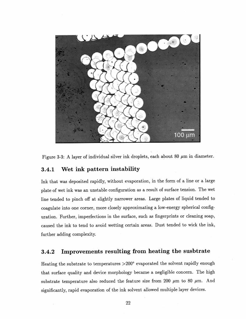
3.4 Printing properties and optimizations
Single layers of a multiple-layer device were achieved by depositing droplets so that
neighboring droplets were as close as possible without touching, as shown in Figure 3-
3. Satellite droplets were eliminated by lowering the magintude of the signal to the
ink jet head. Lower voltages also lead to lower droplet volumes. To lower the ink
viscosity, the ink jet head was heated using resistors in direct thermal communication
with the head.
21
(#
Figure 3-3: A layer of individual silver ink droplets, each about 80 pim in diameter.
3.4.1 Wet ink pattern instability
Ink that was deposited rapidly, without evaporation, in the form of a line or a large
plate of wet ink was an unstable configuration as a result of surface tension. The wet
line tended to pinch off at slightly narrower areas. Large plates of liquid tended to
coagulate into one corner, more closely approximating a low-energy spherical config-
uration. Further, imperfections in the surface, such as fingerprints or cleaning soap,
caused the ink to tend to avoid wetting certain areas. Dust tended to wick the ink,
further adding complexity.
3.4.2 Improvements resulting from heating the susbtrate
Heating the substrate to temperatures >2000 evaporated the solvent rapidly enough
that surface quality and device morphology became a negligible concern. The high
substrate temperature also reduced the feature size from 200 pm to 80 Mm. And
significantly, rapid evaporation of the ink solvent allowed multiple layer devices.
22

Chapter 4
Results
4.1 Droplet specifics
4.1.1 morphology
An atomic-force microscope (AFM) was used to image a disk of silver ink deposited
onto a substrate at 250'C and sintered at 300'C. The image and a cross-section are
presented in Figure 4-1. The disk was approximately 50 nm thick and 82 pm in
diameter.
The cross section of a thicker line of deposited silver was taken with AFM and
the resistance along it was measured. A rough estimate for the electrical conducitivy
was found to be 50x 10 6 - 1m- 1 . This value compares favorably with the bulk con-
ductivity value for silver of 62.9 x 10 6 Q-'m- 1, though the latter result is accurate to
only a single digit because of non-measurable variations in the thickness of the line.
4.1.2 Droplet placement repeatability
A gap between conductive lines of 10 pm was achievable, suggesting an expected
repeatability for droplets of ±5 tm.
23

Figure 4-1: The disc of a single droplet of nanoparticle silver ink imaged with atomic
force microscope. The images, starting at the top, are a perspective view, overhead
vew, and a cross. The vertical dimension is multiplied by a factor of 80 in the
perspective view.
24
--------------- ---------------- L -------------- --------------- ---------------
- - - - - - - - - - - - - - - - - - - - - - - - - - - - - - - - - - - - - - - - - - - - - - - - - - - - - - - - - - - - - - - - - - - - - - - - - -
------- ------- --------------- ---------- -------- ---------

4.2 Basic patterning
Evidence for the ability of ink jet to make larger scale patterns for applications such
as printed circuit boards is shown in Figure 4-2. The image is a photograph of an
ink jet printed 7-segment display driver for electronic ink. Electronic ink is a display
technology invented in our lab that requires only an electrostatic potential to be
applied to change the visual state of the material.[18] The device was printed with
a single layer and printing time was 30 minutes. Substrate temperature was 250*C.
Every connection was functional and the resistance between the contact pads and the
segments of the display had a maximum of 50 Q.
Figure 4-2: Ink jet printed pattern for a 7-segment display driver for E-ink.
The nanoparticle silver ink was found to adhere well to both glass and polyimide.
Nanoparticle gold was found to not adhere as well to gold and was removable with a
fingernail.
4.3 Linear Motor
An explanation for the basis for linear motor operation can be found in section 2.4.1.
The three interdigitated bus lines were fabricated by printing only two on one side
of a 75 pm sheet of polyimide plastic, and printing the third on the other side. The
25

second side was used to avoid the need for a printed insulator material. An image of
the linear drive motor is in Figure 4-3.
Figure 4-3: Ink jet printed linear drive motor printed on polyimide film. Figure shownto scale.
The three interdigitated bus lines were alternately pulsed at 100 V at a frequency
of 0.1 Hz to 10 Hz. By choosing the order of pulsing, dielectric glass balls were
made to move in one direction or the other. Operation was demonsrtrated with both
250 pm balls and 500 pm balls. Figure 4-4 is a sequence of stills taken from a video
of the linear motor in operation. At successive frames, the result of en masse ball
motion is in evidence by their predominance on one side or the other.
Figure 4-4: A series of stills taken from a movie of linear motor operation.
4.4 Radiofrequency identification tag
In Figure 4-5 is a photograph of printed radiofrequency tag that was sensable using a
frequency of 25 MHz. Figure 4-6 is an image of the resonant coil attenuating a small
range of frequencies in the neighborhood of the resonant frequency.
26
I
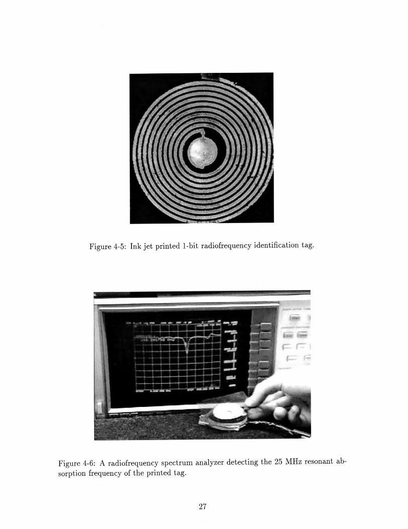
Figure 4-5: Ink jet printed 1-bit radiofrequency identification tag.
Figure 4-6: A radiofrequency spectrum analyzer detecting the 25 MHz resonant ab-
sorption frequency of the printed tag.
27
E
4.5 Electrothermal actuators
4.5.1 In-plane actuator
A material consisting of poly-methyl-methacrylate (PMMA) dissolved in acetone was
found to act as an easily removable sacrificial release material. The PMMA was
pattered using a draw-down bar as diagrammed in Figure 4-7. No solvent was found
that was able to remove photoresist or polyimide films once they were heated to
300 0 C. The PMMA had a sufficiently high crosslink temperature that the sintering
temperature did not affect its dissolvability. However, the a-terpineol solvent in the
nanoparticle ink also dissolved the PMMA and often the silver would bleed through
the release layer and adhere to the glass surface beneath. A very thick layer of PMMA
was required to avoid this.
The draw-down bar was suspended 100 pm above the surface of a glass slide and
slowly pulled over, yielding a thick layer. The cantilever structure was built at the
edge of the PMMA layer so that its base contacts could adhere to the glass and the
cantilever portion stick over the PMMA. The structure material was nanoparticle
silver. During ink jet deposition of the nanoparticle ink, the substrate was heated to
250*C. The droplet frequency was tailored so that no adjacent droplets on the same
"layer" touched, avoiding wet coagulation of the ink. The thick side was made of 120
layers, and the thin side 40.
During the sinter process, the nanoparticle ink tended to shrink by a factor of
20% or more. In the case of the PMMA release layer, the PMMA tended to soften
at the silver's sintering temperature, allowing the cantilever structure to slowly slide
over the surface of the PMMA as it shrunk. It was found later that cracking could be
avoided by heating the deposited material to 250 C for 30 minutes before sintering it
at 300 0C.
The printed device was sintered at 300*C for 10 minutes and then very lightly
sonicated in an acetone bath to dissolve the PMMA release layer. Figures 4-8 and
4-9 are two different views of the in-plane heatuator.
A current-limited power supply was used to drive the actuator. Deflection was
28

Draw-down bar
PMMA
A
B
p ink jet head
C
Figure 4-7: Fabrication process for ink jet printed planar actuator: (A) Deposit of
sacrificial release material. (B) Draw-down. (C) Nanoparticle ink jet deposit and
cure. (D) Removal of sacrificial release layer.
Figure 4-8: Ink jet printed planar electrothermal actuator.
29

Figure 4-9: Alternate view of ink jet printed planar actuator.
as high as 30, or 0.2 mm, before thermal burnout. Power usage was 25 milliwatts at
5 volts. The time constant associated with the decay to steady-state was 50 millisec-
onds. No transient oscillatory behaviour was observed.
4.5.2 Out-of-plate actuator
The out-of-plane actuator was fabricated by layering droplets of ink vertically. Fig-
ure 4-10 is an image of the device.
Figure 4-10: Out-of-plane electrothermal actuator.
As the two towers were built higher, thermal conductivity from the substrate fell,
30

so eventually both were perpetually wet at the top, mushrooming out. The wet-
mushrooming effect eventually caused the two towers to join. As a result of the large
volume of material at the top of the actuator, sintering time was over 30 minutes.
Deflection for this device was negligible.
4.6 Capacitor
A capacitor was built which demonstrated a capacitance of 9±1 pF using a capac-
itance measuring machine. The dielectric insulator was an acetate-based material
designed as a resin for ink jet printing onto nonporous surfaces. The fabrication pro-
cess included ink jet printing a silver bottom plate, depositing the insulator onto a
250*C hotplate with a pipette, and then depositing another layer of conductive silver
on top of the insulator. Layers of the insuating material deposited by ink jet were
shown to insulate, yielding an all ink jet printed capacitor.
Other insulators attempted included photoresists, spin-on-glass, and polyimide.
In all other cases every device fabricated did not insulate. It was postulated that
conduction was the result of cracking, pinhole defects, or the solvent in the ink dis-
solving the insulating material. Ink jet printing of photoresist, spin-on-glass, and
polyimide were demonstrated.
31

Chapter 5
Conclusion
The goal of this project was to show that nanoparticle ink jet fabrication could be
used to build devices of sufficient electrical and mechanical quality and repeatability
to suggest the process could be used as an alternative fabrication system to vacuum-
deposited CMOS and MEMS-type processes at far lower cost.
5.0.1 Cost
The nanoparticle material was purchased at a price of $55 per gram. Using an estimate
of a 10 minute printing time and continuous droplet ejection at 125 Hz, 10% weight
ink, 1 kg/L ink density, and an 80 pL droplet volume, the expected cost of the material
in a simple device such as a linear motor is 3 cents. Considering a standard MEMS
foundary cost of roughly $3000 per square centimeter for a standard process, and a
turn around time of two months, the potential is there for an alternate approach such
as ink jet to offer a revolution in speed and cost.
Considering that all processing temperatures for the devices were below 300'C, in
earth atmosphere, the costs associated with building a device with nanoparticles can
be expected to be far lower than vacuum processes.
32

5.0.2 Performance
The conductivity of the nanoparticle silver ink jet deposited film was within a factor of
two of that of builk silver. That the micromechanical actuator was physically strong
enough to withstand sonication, and further was able to deflect and resume its position
is indication of mechanical strength. In addition, the vertically printed actuator
suggests the ability to print very complex mechanical structure. The results achieved
with nanoparticle material films in this report and others suggests printing to be a
process that can yield results far in excess of those achievable with organic chemistry
means, and of sufficient quality to be used in integrated-circuit type applications.
A concern is device shrinkage. On average shrinkage was 25% with a rapid sinter.
At lower sinter temperatures over extended periods of time, such as 250 C was found
to allow more vertical shrinkage with less cracking. However, it is expected that
more complex devices will require shrinkage compensation (such as the type used for
inkjection molded parts) or an improved material that shrinks less.
The mechanical actuator result was presented to the IEEE Micro-Electromechanical
Systems 2000 conference in Japan in January.[19]
5.0.3 The limits of size
Figure 5-1 is an image of a 5 pm silver droplet generated inadvertently as a result of
a microscopic ink "splash." It shows the potential for much smaller ink droplets to
be used to make devices with feature sizes competetive with lithographic techniques.
5.1 Applications
This work has received a fair amount of interest from companies interested in inex-
pensive tag technology, as well as from groups interested in systems for one-off and
extremely inexpensive integrated circuits. Considering the far lower costs for the
ink jet process in combination with its demonstrated high device quality, ink jet has
much promise for being the process used for a desktop MEMS and or integrated cir-
33

Figure 5-1: Ink droplet at 4000 dpi generated from a splash demonstrates feature size
comparable to those attained by lithography.
cuit fabrication system where cost, device bulk, and turnaround time are significant
factors.
34
Appendix A
Program for Printing Planar
Electrothermal Actuator
The following is a verbatim reproduction of the program used to print the electrother-
mal actuators of Section 4.5.
; thermal-actuator6.prg
; Sawyer Fuller 4/24/00
; Builds an ink jet printed electrothermal actuator onto a glass slide.
; Manually-set origin is at edge of release layer so that contact pads are
adhered to slide.
post-print: heat at 250 C for 30 minutes before releasing to
avoid cracking
nozzle droplet frequency 125Hz
v6 = 27v9 =30v12 = 12su :initialize
v50 = v50 + 16v51 = v51 + 25su :toorigin
:heatuator
:contact-pads
; nozzle number for print head (0 is leftmost, 47 is rightmost); nozzle for photoresist (insulator) head, head 2; nozzle number for trident head (1 is rightmost, 16 is leftmost)
; add offset to where edge of relase material is
Start of heatuator section.
Origin is base of cantilever to allow easy registration
to edge of release layer. Just measure metric position on slide.
35

loop 8 ; layers of contact pads
su :toorigin ; to x,y,z coordinates specified in variables v50, vS1, and v52
v101 = 2.95 ; x and y contact pad dimension variables
v102 = .6li x=(-v10l) y=(-.6)
su :platehoriz ; build a plate structure with x-direction strokes - padi
li x3.1
su :plate-horiz ; pad2next ; layer of contact pads
:cantilevers ; cantilever section
loop 40 ; passes of cantilever structure
su :toorigin
Thick half of cantilever.
Three times as thick.
li x=(-.1) y(-.6)v104 = v232
li y-3.1
su :line-vert
y=(-2+.135) fv4
su :line-vert-backwards
y=(2-.135) fv4
su :line-vert
li y=(3.1 - 8) fv4 ; move to horiz bar position
li y-.05 ; kluge
:crossbar ; build structure at tip of cantilever
loop 3 ; 3 lines of width make up the tip
v104 = .30 ; tip made of from short line procedure
; makes the tip stiff structurally
su :shortline-horiz.here
li y-.05
next ; layer of tip structure
su :toorigin ; recenter, do the thin half of the can
li x=(.1) y(-.6)
v104 = v232su :line-vert-here
su :cure-pause ; move out of the way and pause for sol
su :toorigin
next ; cantilever layer
tilever
vent to evaporate
:donesu :endsu :allon ; turn on all nozzles once finished so they don't dry out
exit ;******************************************************************
:initialize
-- > feedrate, etcvO = 0 ; throwaway variable for user interrupted pauses, etc.
v4 = 10000 ; off feedrate
36

; -- > head positioning stuffv5 = 1.397 ; inter-nozzle spacing for silver dpc head
v54 = -0.594/10*25.4 ; inter-nozzle spacing for trident head
;v6 is at top of program now
v7 = v5 * v6 ; y-offset for nozzle in use
V8 = 0 ; x-offset to get to this nozzle
; v9 is at top now
v10 = v5 * v9 + .6 ; offset for which nozzle in head 2
vii = 50.8 ; x-offset to get to this nozzle
; v12 is at top now ; nozzle in use in head 3 - trident head
v13 = v54 * v12 + 72 + 0.404*25.4; y-offset for nozzle number plus initial offset in head
v14 = 95 + 0.113*25.4 + 0.5 ; x-offset to get to trident head position
; from dpc head position
v15 = 0 ; corresponds to which output to use when switching between
active ink jet heads
; --> misc
v40 = 1 ; thickness of substrate
v50 = 180 + .4 ; x-offset for relative 0 position, varies throughout program
v51 = v7 + 58-5*v5 + 2.2; y-offset for relative 0 position, varies
v52 = 3.5 - v40 ; z-offset for relative 0 position, varies
-- > actuator specific stuff
v232 = 3 ; length of cantilever
-- > other stuffvelocity off
su :allon ; default state is for all heads to be on to avoid drying out
output V15,1 ; except turn off the default active head
wait off
velocity off
fv4 ; set to free run feedrate
return
:set-hotplate300 ;set hotplate to 300C
wait on
com free
wait on
com init 1,8,1,n,9600 ;9600 bps com 333333
wait oncom send "= SP1 300 /c13"
return
:set-hotplate_200 ;set hotplate to 200C
wait on
com freewait on
com init 1,8,1,n,9600 ; 9600 bps com 3wait on
com send "= SP1 200 /c13"
return
37

:switch-to-trident-head
su :alloff
v15 = 3li xvl4 y=(-v7 + v13)v50 = v50 + v14v51 = v51 - v7 + v13output 0,0
return
; v15 says which head is currently active; move new nozzle to same position over substrate; reset origin value: x; reset origin value: y; turn on dpc head to keep from drying out
:switch-to-first _dpc-head ; usually the silver ink jet head
su :alloffv15 = 0 ; which head is active
li x-v14 y=(v7 - v13) ; move new nozzle to same position over substrate
v5O = v5O - v14 ; reset origin values v50 v51 v52
v51 = v51 + v7 -v13output 3,0 ; turn on trident head to keep from drying out
return
:alloffoutput 0,1
output 2,1
output 3,1
fv4
return
:allon
output 0,0
output 2,0
output 3,0
fv1return
:cure-pausewait on
su :off
su :away
su :on
loop 1
li x1 f80
li x-1 f80
next
su :off
su :return-from-away
wait off
return
:away ; move the printhead assembly out of the way
38

if v15 = 3 :dumboffaway ; do this weird procedure if trident head is activeli x-150 y-60 fv4goto :awayend
: dumboff awayoutput 0,1
output 2,1
ii x-240 y-100 fv4
output 0,0
output 2,0
:awayend
return
:return-from-away
if v15 = 3 :dumboffreturn ; same explanation as in previous subroutine
li x150 y60 fv4goto :return-from-awayend
:dumboffreturn
output 0,1
output 2,1
li x240 y100 fv4output 0,0
output 2,0
:return-from-awayend
return
:on
fv1output v15,0
return
:off
output v15,1
fv4
return
:toorigin
su :off
velocity off
pr ab ; absolute coordinates
li zv52
li x=v50 y=v51
pr in ; back to incremental coordinates
return
:end
su :alloff
pr ab ; absolute coordinates
su :off
39

velocity off
li xO y0 zO
pr in ; back to incremental coordinates
su :allon
home x y z
su :alloff
su :toorigin
su :away
return
:shortline-horiz-here
; v104 specifies length
; couple of drops every 30 microns
; assume 125 hz drop rate
vO = 1/250*1000 ; time dwell duration in ms
v234 = cvi(v104/.060) ; integer division
loop v234
output v15,0
dwell vO
output v15,1
li x=.060
next
li x=(-v234 * .060)
return
:line.horiz
Makes a line v104 mm long starting 3.1mm away from current position.
Path ends v104+8 mm away.
f800
velocity on ; use this weird procedure to start moving gantry before
; turning on the ink nozzle so full speed is achieved before droplets
start.
li x4
output v15,0 ; on
li xv104
output v15,1 ; off
velocity off
li x4
fv4
return
:line-vert
f800
velocity on
li y4
output v15,0 ; on
li yv104
output v15,1 ; off
40

velocity off
li y4
fv4
return
:line-horiz-herePut horiz line starting from current position and ending at current position.Better for abstraction but slower.
li x-3.1 fv4
su :line-horiz
li x=(-v104 - 8 +3.1) fv4
return
:line-vert-here
li y-3.1 fv4
su :line-vert
li y=(-v104 - 8 +3.1) fv4
return
:line-horiz-backwards
f800
velocity on
li x-4
output v15,0 ; on
li x=(-v104)
output v15,1 ; off
velocity off
li x-4
fv4
return
:line-vert-backwards
f800
velocity on
li y-4
output v15,0 ; on
li y-v104
output v15,1 ; off
velocity off
li y-4
fv4
return
:trace-horiz
; trace .20 mm wide
li x-3.1
loop 2
su :line-horiz
41

li y.05 x=(-2+.135) fv4
su :line.horiz-backwards
li y.05 x=(2-.135) fv4
next
li y-.20 x3.1
return
:line-vert.here-backwards
li y3.1 fv4
su :line-vert-backwards
li y=(v104 +8 -3.1) fv4
return
:plate.horizprints a plate structure using a series of x-direction passes
v101 = width; v102 = height
v104 = v101vO = cvi(v102/.20)loop vO
su :trace-horiz
li y.20
su :cure.pause
next
li y=(-.20 * vO)
return
; integer divide
; height of plate
42

Bibliography
[1] Paul A. Williams. Three dimensional printing: A new process to fabricate pro-totypes directly from cad models. Master's thesis, Massachusetts Institute ofTechnology, 1990.
[2] David B. Wallace and Donald J. Hayes. Solder-jet technology update. SPIEInternational Symposium on Microelectronics, pages 681-684, 1997.
[3] Gregg Duthaler. Design of a drop-on-demand delivery system for molten soldermicrodrops. Master's thesis, Massachusetts Institute of Technology, 1995.
[4] Fuquan Gao. Molten Microdrop Deposition and Solidification Processes. PhDthesis, Massachusetts Institute of Technology, 1994.
[5] T. R. Hebner, C. C. Wu, D. Marcy, and et. al. Ink-jet printing of doped polymersfor organic light emitting devices. Applied Physics Letters, 72:519-521, 1998.
[6] Shun-Chi Chang, Jayesh Bharathan, Yang Yang, and et. al. Dual-color polymerlight-emitting pixels processed by hybrid inkjet printing. Applied Physics Letters,73(18):2561-2563, 1998.
[7] G6khan Perin, Thomas S. Lundgren, and Butrus T. Khuri-Yakub. Controlledink-jet printing and deposition of organic polymers and solid particles. AppliedPhysics Letters, 73(16):2375-2377, 1998.
[8] Kien F. Teng and Robert W. Vest. A microprocessor-controlled ink jet print-ing system for electronic circuits. IEEE Transactions on Industrial Electronics,35(3):407-411, 1988.
[9] J. Heinzl and C. H. Hertz. Ink-jet printing. Advances in Electronics and ElectronPhysics, 65:91-171, 1985.
[10] Brent Ridley, Babak Nivi, and Joseph Jacobson. All-inorganic field effect tran-sistors fabricated by printing. Science, 286:746-749, 1999.
[11] Brent Ridley. Inorganic semiconductors for printed transistors. Master's thesis,Massachusetts Institute of Technology, 1999.
[12] A. P. Alivisatos. Semiconductor clusters, nanocrystals, and quantum dots. Sci-ence, 271:933-937, 1996.
43

[13] Ph. Buffat and J. P. Borel. Size effect on the melting point of gold particles.Physical Review A, 13(6):2287-2298, 1976.
[14] A. N. Goldstein. The melting of silicon nanocrystals: Submicron thin-film struc-
tures derived from nanocrystal precursors. Applied Physics A, 62:33-37, 1996.
[15] H. Guckel, J. Klein, T. Christenson, and et. al. Thermo-magnetic metal flexureactuators. Technical Digest, Solid State Sensor and Actuator Workshop, HiltonHead, SC, USA, 13-16 June 1992, pages 73-75.
[16] John H. Comtois and Victor M. Bright. Applications for surface-micromachinedpolysilicon thermal actuators. Sensors and Actuators A Physical, 58:19-25, 1997.
[17] John. H. Comtois, Victor. M. Bright, and M. Phipps. Thermal micro-actuatorsfor surface-micromachining processes. Proc. SPIE, Vol. 2462, Micromachined
Devices and Components, pages 10-21, 1995.
[18] Barret Comiskey, J. D. Albert, Hidezaku Yoshizawa, and Joseph Jacobson. An
electrophoretic ink for all-printed reflective electronic displays. Nature, 394:253-255, 1998.
[19] Sawyer Fuller and Joseph Jacobson. Ink jet fabricated nanoparticle mems. In
Proceedings of IEEE Micro-electromechanical Systems, pages 138-141, 2000.
44