
Initial Report on Specification Testing Effectiveness
40
Initial Report on Specification Testing Effectiveness Deliverable 1.4a, TAMES-2, IST Project 2001-34283 Version 1.2, March 2004 Contact Author: A. Lechner Authors: K. Georgopoulos, M. Burbidge, A. Lechner, D. De Venuto 1 , Eric Compagne & A. Richardson 1 On secondment from the Politecnico Di Bari, Italy Testability of Analogue Macrocells Embedded in System-on-Chip
Transcript of Initial Report on Specification Testing Effectiveness

Initial Report on Specification Testing
Effectiveness
Deliverable 1.4a, TAMES-2, IST Project 2001-34283
Version 1.2, March 2004
Contact Author: A. Lechner
Authors: K. Georgopoulos, M. Burbidge, A. Lechner, D. De Venuto1, Eric Compagne & A. Richardson 1 On secondment from the Politecnico Di Bari, Italy
Testability of Analogue Macrocells Embedded in System-on-Chip

TAMES-2 D1.4a, Version 1.2 Testability of Analogue Macrocells Embedded in System-on-Chip
I
List of Content Initial Report on Specification Testing Effectiveness ..........................................................................1
1 Introduction ....................................................................................................................................1
2 Polynomial Fitting Algorithm Test Method .................................................................................2
2.1 Fitting Algorithm and Test Method Theory..............................................................................2 2.2 Stimulus Generation and Test Evaluation.................................................................................3 2.3 Further Work ............................................................................................................................5
3 Walsh Analysis................................................................................................................................6
3.1 Walsh Transform Theory..........................................................................................................6 3.2 Walsh Transform ....................................................................................................................10 3.3 Fast Walsh Transform.............................................................................................................10 3.4 Power Calculation from FWT Results ....................................................................................11 3.5 Example Synthesis using Walsh and Fourier Series ...............................................................11 3.6 Walsh Transform Example .....................................................................................................12 3.7 Walsh Test Solution................................................................................................................13 3.8 Assessment of Applicability and Test Coverage ....................................................................16
3.8.1 Sensitivity to Input Stimulus Accuracy ..........................................................................16 3.8.2 Coverage Against Performance Parameter Failure .........................................................18
3.9 Application and Integration of Walsh Testing........................................................................21 3.10 Summary and Future Work.....................................................................................................25
4 Distortion Meter Method .............................................................................................................27
5 Noise Transfer Function Test ......................................................................................................29
5.1 Gain Evaluation Measuring the Noise Transfer Function Attenuation...................................31 5.2 SNR Measurement..................................................................................................................31 5.3 Measuring THD......................................................................................................................33
6 Summary .......................................................................................................................................35
7 References .....................................................................................................................................36

TAMES-2 D1.4a, Version 1.2 Testability of Analogue Macrocells Embedded in System-on-Chip
II
List of Figures Figure 1: Signal generated by the PWM with an FPGA.......................................................................4 Figure 2: Test signal generated after a low pass filtering .....................................................................4 Figure 3: Set of Walsh functions in sequency order [BEA75] .............................................................7 Figure 4: Set of Walsh functions in “natural” order [BEA75] .............................................................8 Figure 5: Signal flow diagram for FWT (sequency ordered, Larsen’s FWT) [BEA75].....................10 Figure 6: Synthesis of continuous seismic waveform [BEA75].........................................................12 Figure 7: Synthesis of rectangular waveform [BEA75] .....................................................................12 Figure 8: FWT program [BEA75]......................................................................................................13 Figure 9: Walsh and Fourier transform results for PCM waveform [BEA75] ...................................14 Figure 10: FFT and Walsh results on modulator bit-stream with sine wave input ..............................15 Figure 11: FFT and Walsh results on modulator bit-stream with square wave input ..........................15 Figure 12: Walsh power spectrum for 214 and 216 samples (2.0 V amplitude) .....................................19 Figure 13: SNR through Walsh – preliminary simulation results ........................................................21 Figure 14: Walsh power spectrum for failure in SNR (preliminary results) ........................................21 Figure 15: System representation .........................................................................................................21 Figure 16: Implementation of full parallel FWT ..................................................................................22 Figure 17: Implementation of parallel feedback FWT .........................................................................22 Figure 18: Implementation of serial feedback FWT.............................................................................23 Figure 19: Cross coupled double input sampling [PLA03] ..................................................................25 Figure 20: Functional description of the distortion meter method .......................................................27 Figure 21: Behavioural simulation result. E is the input signal, Fir3_out is the reconstruction of the
ADC output and Notch2_out is the output of the second notch..........................................27 Figure 22: Noise transfer function of a 4th order modulator ................................................................29 Figure 23: New test access for a 4th order sigma-delta modulator ......................................................29 Figure 24: FFT at the output of the ADC, at S1, S2 S3, S4 .................................................................30 Figure 25: As in Figure 24, distortion applied at the first block...........................................................30 Figure 26: As in Figure 24, distortion applied at the second block. .....................................................30 Figure 27: As in Figure 24, Distortion applied in each block...............................................................30 Figure 28: Low pass filtering (straight red line) used to measure the quantisation noise.....................32 Figure 29: FFT over 65536 samples: S/(N+THD) = 0.6dB..................................................................32 Figure 30: FFT at the converter output when the SUM node is stimulated ..........................................33 Figure 31: FFT at the converter output when the SUM node is stimulated and the distortion is
assumed...............................................................................................................................34
TAMES-2 D1.4a, Version 1.2 Testability of Analogue Macrocells Embedded in System-on-Chip
III
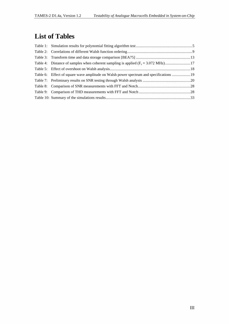
List of Tables Table 1: Simulation results for polynomial fitting algorithm test ..........................................................5 Table 2: Correlations of different Walsh function ordering...................................................................9 Table 3: Transform time and data storage comparison [BEA75] ........................................................13 Table 4: Distance of samples when coherent sampling is applied (Fs = 3.072 MHz)..........................17 Table 5: Effect of overshoot on Walsh analysis...................................................................................18 Table 6: Effect of square wave amplitude on Walsh power spectrum and specifications ...................19 Table 7: Preliminary results on SNR testing through Walsh analysis .................................................20 Table 8: Comparison of SNR measurements with FFT and Notch......................................................28 Table 9: Comparison of THD measurements with FFT and Notch .....................................................28 Table 10: Summary of the simulations results.......................................................................................33

TAMES-2 D1.4a, Version 1.2 Testability of Analogue Macrocells Embedded in System-on-Chip
1
1 Introduction A/D converters are one of the most frequently used mixed-signal circuits. High-resolution A/D converters are precision products and their test usually requires high quality test equipment. With advances in their performance, the required test equipment is becoming increasingly expensive while test times are escalating.
Deliverable 1.1 [TAM02] describes five of the most mature conventional A/D converter testing techniques and discusses their advantages and disadvantages with regard to high-resolution converter testing also in terms of potential for on-chip integration. Further information can be found in IEEE standards, (“1241-2000 IEEE Standard for Terminology and Test Methods for Analog-to-Digital Converters” [IEE01] and “1057-1994 IEEE Standard for Digitizing Waveform Recorders" [IEE94, IEE04]) or [BUR01, MAH87, PLA03].
The analysis in D1.1 led to the conclusion that high-resolution A/D converter performance can be tested conventionally through either the histogram test methodology or FFT analysis, where histogram testing verifies static performance parameters while FFT-based testing assesses dynamic performance parameters. However, for conventional histogram testing of high-resolution converters, the test time escalates due to the large number of samples required for DNL and INL calculation. Similarly, to accurately assess dynamic performance parameters of high-resolution converters, the required number of samples for FFT analysis increases to 65536 as shown in D2.1a [TAM03] and included in the reference test plan for the hiCOD design [TAM04-1]. Neither of the conventional test methodologies is suitable for straight-forward on-chip implementation due to unacceptable area overhead [TAM02]. Additionally, an on-chip implementation would not decrease the kernel test time of either test technique.
For any novel test technique, an in-depth study needs to be performed to validate its coverage against performance parameter failure. This deliverable documents the assessment of dynamic specification testing effectiveness for the following test approaches:
• Polynomial fitting algorithm
• Walsh analysis
• Distortion meter test methodology
• Noise transfer function test
The studies, in particular for the Walsh transform test method, extensively use the results of the failure mode investigations documented in D1.2 [TAM04] and D1.3 [TAM02-1]. Each of the techniques is assessed for its effectiveness in testing converter specifications in the following chapters. Results of the investigations lead to the construction of the corresponding decision matrices [TAM04-1]. A summary of results is provided in section 6.
This is an initial report on specification testing effectiveness (D1.4b is the final report). Throughout the document, work in progress is described and analysed and future aspects are discussed.

TAMES-2 D1.4a, Version 1.2 Testability of Analogue Macrocells Embedded in System-on-Chip
2
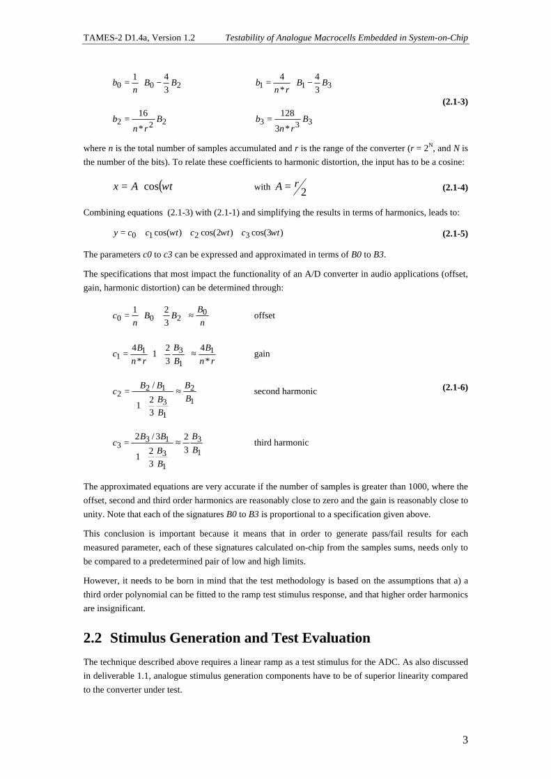
2 Polynomial Fitting Algorithm Test Method An interesting technique is presented in [ROY02, SUN97] and also considered within TAMES-2. The technique proposes a digital generation of an analogue waveform suitable for BIST of high-resolution A/D converters. The proposed test signal is a staircase-like exponential waveform. It is shown in [SUN97] to have properties of a perfectly linear ramp when used as the stimulus for a third order polynomial fitting algorithm that measures offset, gain, 2nd and 3rd harmonic distortion. The technique is particularly suitable for testing high resolution converter (>16-bit) even in a noisy environment. First simulations results for an ideal 16-bit sigma-delta converter are shown here. Using the test signal proposed in [ROY02] and with just 2000 samples then reducing the time test normally spent to perform an FFT which requires higher number of samples and a subsequence mathematical evaluation it is possible to evaluate gain, offset, 2nd and 3rd harmonics in a total test time of 0.238 s (for 44 kHz). Shorter test time can be achieved by sampling at the output of the bit stream but additional manipulation of the samples has to be performed by software and the decimator will not be considered in the test.
2.1 Fitting Algorithm and Test Method Theory In [SUN97] a third order polynomial fitting algorithm is applied to the output samples of an A/D converter for a perfectly linear ramp input stimulus. It is shown that the four coefficients of the best-fit polynomial are mathematically related to four key performance parameters for the converter: offset, gain, second and third order harmonic distortion.
The amplitude of the stimulus ramp covers the full input range of the A/D converter during the time it takes to gather the required number of samples at full conversion speed. The total sampling time is divided into four equal intervals during which the samples are accumulated, rendering four sums at the end of the sampling process: S0, S1, S2, and S3.
A relationship between the third order polynomial and these sums is demonstrated in [SUN97]. A third order polynomial is given as:
33
2210 xbxbxbby +++= (2.1-1)
From the four sum of samples (S0 to S3), four signatures (B0 to B3) are derived as simple linear combinations:
01233
01232
01231
01230
33 SSSSBSSSSB
SSSSBSSSSB
−+−=+−−=−−+=+++=
(2.1-2)
These four equations can be easily and economically calculated on-chip through digital circuitry. The coefficients of the polynomial (2.1-1) are proven to be connected to the coefficient of the polynomial fitting by [SUN97]:
TAMES-2 D1.4a, Version 1.2 Testability of Analogue Macrocells Embedded in System-on-Chip
3
−= 200 3
41BB
nb
−= 311 3
4*4
BBrn
b
222*
16B
rnb = 333
*3
128B
rnb =
(2.1-3)
where n is the total number of samples accumulated and r is the range of the converter (r = 2N, and N is the number of the bits). To relate these coefficients to harmonic distortion, the input has to be a cosine:
( )tAx ωcos⋅= with 2rA = (2.1-4)
Combining equations (2.1-3) with (2.1-1) and simplifying the results in terms of harmonics, leads to:
)3cos()2cos()cos( 3210 tctctccy ωωω +++= (2.1-5)
The parameters c0 to c3 can be expressed and approximated in terms of B0 to B3.
The specifications that most impact the functionality of an A/D converter in audio applications (offset, gain, harmonic distortion) can be determined through:
nB
BBn
c 0200 3
21≈
+= offset
rnB
BB
rnB
c*
432
1*
4 1
1
311 ≈
+= gain
1
2
1
3
122
32
1
/BB
BB
BBc ≈
+
= second harmonic
1
3
1
3
133 3
2
32
1
3/2BB
BB
BBc ≈
+
= third harmonic
(2.1-6)
The approximated equations are very accurate if the number of samples is greater than 1000, where the offset, second and third order harmonics are reasonably close to zero and the gain is reasonably close to unity. Note that each of the signatures B0 to B3 is proportional to a specification given above.
This conclusion is important because it means that in order to generate pass/fail results for each measured parameter, each of these signatures calculated on-chip from the samples sums, needs only to be compared to a predetermined pair of low and high limits.
However, it needs to be born in mind that the test methodology is based on the assumptions that a) a third order polynomial can be fitted to the ramp test stimulus response, and that higher order harmonics are insignificant.
2.2 Stimulus Generation and Test Evaluation The technique described above requires a linear ramp as a test stimulus for the ADC. As also discussed in deliverable 1.1, analogue stimulus generation components have to be of superior linearity compared to the converter under test.
TAMES-2 D1.4a, Version 1.2 Testability of Analogue Macrocells Embedded in System-on-Chip
4
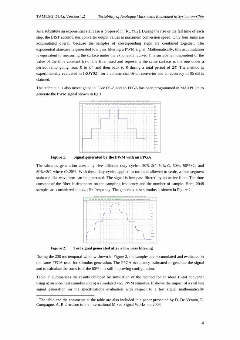
As a substitute an exponential staircase is proposed in [ROY02]. During the rise or the fall time of each step, the BIST accumulates converter output values at maximum conversion speed. Only four sums are accumulated overall because the samples of corresponding steps are combined together. The exponential staircase is generated low pass filtering a PWM signal. Mathematically, this accumulation is equivalent to measuring the surface under the exponential curve. This surface is independent of the value of the time constant (t) of the filter used and represents the same surface as the one under a perfect ramp going from 0 to r/4 and then back to 0 during a total period of 2T. The method is experimentally evaluated in [ROY02], for a commercial 16-bit converter and an accuracy of 85 dB is claimed.
The technique is also investigated in TAMES-2, and an FPGA has been programmed in MAXPLUS to generate the PWM signal shown in fig.1
SMASH 4.4.1 - Transient C:\Dolphin\smash441\examples\Nuova cartella\RCgeneration.cir - Sat Jan 18 23:32:03 2003
V(1)
10m 20m 30m 40m 50m 60m 70m 80m 90m 100m 110m 120m 130m 140m 150m 160m 170m 180m 190m 200m 210m
-400mV
0V
400mV
800mV
1.2V
1.6V
2V
2.4V
2.8V
3.2V
3.6V
4V
4.4V
4.8V
5.2V
Figure 1: Signal generated by the PWM with an FPGA
The stimulus generation uses only five different duty cycles: 50%-2C, 50%-C, 50%, 50%+C, and 50%+2C, where C<25%. With these duty cycles applied in turn and allowed to settle, a four-segment staircase-like waveform can be generated. The signal is low pass filtered by an active filter. The time constant of the filter is dependent on the sampling frequency and the number of sample. Here, 2048 samples are considered at a 44 kHz frequency. The generated test stimulus is shown in Figure 2.
SMASH 4.4.1 - Transient C:\Dolphin\smash441\examples\Nuova cartella\RCgeneration.cir - Sat Jan 18 23:42:41 2003
V(2)
t = 87.87ms, dt = 20.64ms, y = 3.118V, dy = -890.2mV, frequency = 48.44Hz, slope = -43.110m 20m 30m 40m 50m 60m 70m 80m 90m 100m 110m 120m 130m 140m 150m 160m 170m 180m 190m 200m 210m
-400mV
0V
400mV
800mV
1.2V
1.6V
2V
2.4V
2.8V
3.2V
3.6V
4V
4.4V
4.8V
5.2V
Figure 2: Test signal generated after a low pass filtering
During the 230 ms temporal window shown in Figure 2, the samples are accumulated and evaluated in the same FPGA used for stimulus generation. The FPGA occupancy estimated to generate the signal and to calculate the sums is of the 60% in a still improving configuration.
Table 11 summarises the results obtained by simulation of the method for an ideal 16-bit converter using a) an ideal test stimulus and b) a simulated real PWM stimulus. It shows the impact of a real test signal generation on the specifications evaluation with respect to a test signal mathematically 1 The table and the comments at the table are also included in a paper presented by D. De Venuto, E. Compagne, A. Richardson to the International Mixed Signal Workshop 2003

TAMES-2 D1.4a, Version 1.2 Testability of Analogue Macrocells Embedded in System-on-Chip
5
generated. The total sampling time is divided into four equal intervals during which the samples are accumulated, rendering four sums at the end of the sampling process, i.e. S0 to S3. By fitting a third order polynomial and simplifying the generated equations it is possible to derive the signatures B0 to B3, and the converter’s performance parameters as described above.
The on-chip implementation of the technique has been assessed using an FPGA simulation. In the simulation, where a commercial FPGA 10K1010 FLEX ALTERA was considered, 60% of cells where used for stimulus generation and response evaluation up to calculation of the test signatures. The computation of specifications and comparison to thresholds was considered to be off-chip.
Table 1: Simulation results for polynomial fitting algorithm test
Parameter Real [LSB] Ideal [LSB] S0 -1,23E+07 -1,23E+07 S1 -4,12E+06 -4,11E+06 S2 4,11E+06 4,11E+06 S3 1,23E+07 1,23E+07 n 2008 2008 r 65536,00 65536,00 B0 -16381,37 0,00 B1 32908941,31 32899072,00 B2 46,60 0,00 B3 -370,14 0,00 c0 -8,158053 0,000000000 c1 1,000300 1,000000000 c2 0,000001 0,000000000 c3 -0,000007 0,000000000
offset -0,004063 0,000000000 gain 1,000300 1,000000000 2nd harmonics 0,000001 0,000000000 3rd harmonics -0,000007 0,000000000
2.3 Further Work Future work on this test solution will need to include an assessment of test accuracy and coverage against failure modes discussed in deliverable D1.2. In particular, the impact of the test approach’s underlying assumption (see above) requires further analysis. Example failure modes with significant higher order harmonics have been identified [TAM04]. Simulations can be carried out for the target design affected by these to assess the impact on computed performance parameter values.
TAMES-2 D1.4a, Version 1.2 Testability of Analogue Macrocells Embedded in System-on-Chip
6
3 Walsh Analysis The following sections introduce the theory on Walsh transforms, the discrete Walsh transform algorithms, and power spectrum calculation. A comparison the FFT is included and example syntheses are provided. The Walsh test solution is described and simulation results are discussed regarding coverage against performance parameters and dependencies on stimulus accuracy. Finally Walsh testing is discussed in the context of potential on-chip implementation including the presentation of several implementation concepts for the test evolution.
The motivation the investigation is that FFT converges rapidly to sine wave hence use for classic S/(N+THD) while Walsh transforms converge rapidly to square wave. The idea is to use square wave for input to modulator. The Walsh transform of bit-stream should give a single spectral peak. All other peaks in spectrum are due to noise and non-idealities, and test results should allow conclusions on SNR performance. There may be the need for alternative THD calculations and further work on mapping of test results to convetional dynamic performance parameter testing, see [TAM02].
3.1 Walsh Transform Theory This section briefly introduces Walsh functions and associated theory. Far more detailed material can be found in [BEA75, BEA87]. A historic view, plenty of further references, applications examples, and a comparison to Fourier theory can be found in paper [STO91].
While the Fourier series uses orthogonal sine and cosine functions, the Walsh functions are an ordered set of rectangular waveforms. The Fourier theory is particularly suitable for representing waveforms consisting of sinusoids, while the Walsh theory is better suited for representing waveforms with sharp discontinuities e.g. square waves or pulse density modulated signals. Typical applications of the Walsh sequences include code division multiplexing (spreading de-spreading) and decomposition or synthesis of signals.
The Walsh functions mentioned above form an ordered set of rectangular orthogonal waveforms with only two amplitude values (+1, –1). Any given signal can be represented through the combination of two or more Walsh functions. The discrete Walsh functions of N = 2 p terms can be given as:
( ) ( ) ( )∏−
=
+−−−−
+−−−=1
0021021
111,;,WALp
r
ttnpppp
rrrptttnnn KK (3.1-1)
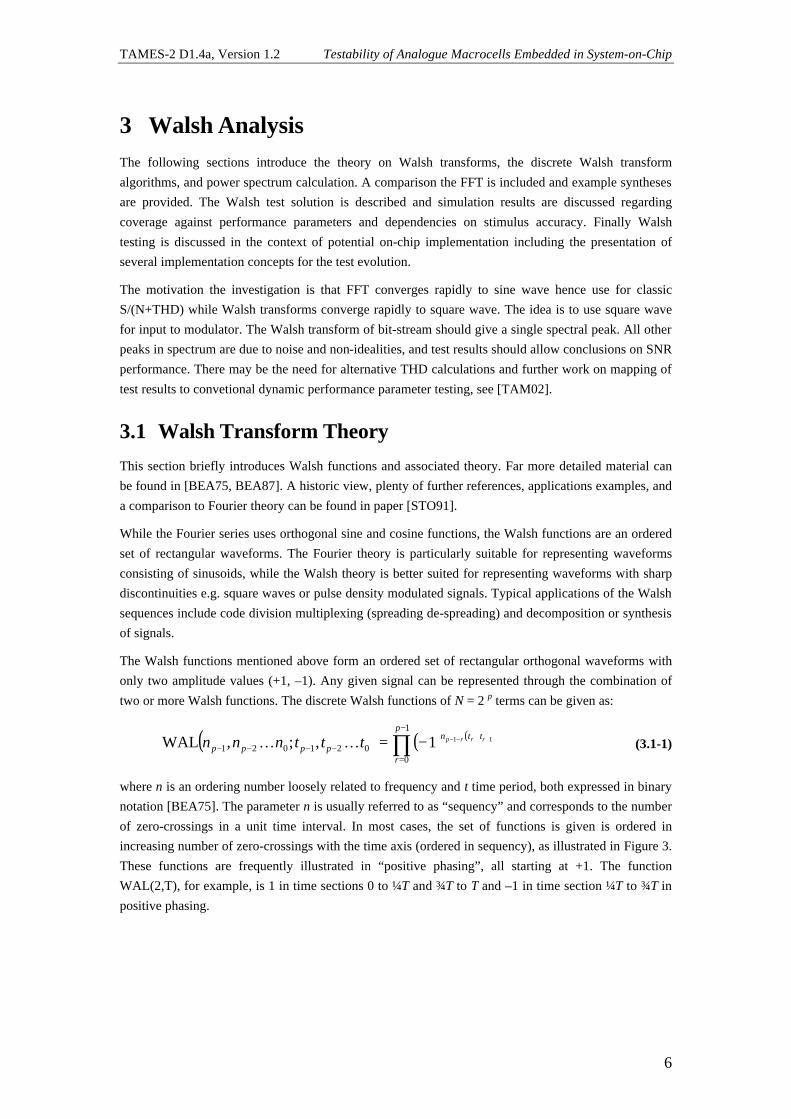
where n is an ordering number loosely related to frequency and t time period, both expressed in binary notation [BEA75]. The parameter n is usually referred to as “sequency” and corresponds to the number of zero-crossings in a unit time interval. In most cases, the set of functions is given is ordered in increasing number of zero-crossings with the time axis (ordered in sequency), as illustrated in Figure 3. These functions are frequently illustrated in “positive phasing”, all starting at +1. The function WAL(2,T), for example, is 1 in time sections 0 to ¼T and ¾T to T and –1 in time section ¼T to ¾T in positive phasing.

TAMES-2 D1.4a, Version 1.2 Testability of Analogue Macrocells Embedded in System-on-Chip
7
1
0 1/2 1
-1
T
SAL(4,T)
CAL(3,T)
SAL(3,T)
CAL(2,T)
SAL(2,T)
CAL(1,T)
SAL(1,T)
CAL(0,T)
WAL(7,T)
WAL(6,T)
WAL(5,T)
WAL(4,T)
WAL(3,T)
WAL(2,T)
WAL(1,T)
WAL(0,T)
Figure 3: Set of Walsh functions in sequency order [BEA75]
Fourier – Walsh Series Comparison
The Fourier series expansion can be given as:
tdtktfT
btdtktfT
adttfT
a
tkbtkaa
tf
T
k
T
k
T
kk
k
∫∫∫
∑
===
++=∞
=
0 00 00
0
01
00
sin)(2
; cos)(2
; )(1
2
where))sin()cos((2
)(
ωω
ωω (3.1-2)
where the time series f(t) is expressed as the sum of a series of sine-cosine functions each multiplied by a coefficient, ak and bk, representing the peak amplitude of that spectral component.
The Walsh series can be given as:
∫∫
∑
==
+=−
=
T
n
T
N
nn
dttntfT
adtttfT
a
tnatatf
00
0
1
10
),(WAL)(1
; ),0(WAL)(1
2
where),(WAL),0(WAL)( (3.1-3)
As in Fourier theory Walsh functions can be expressed in terms of even CAL and odd SAL waveform symmetry hence,
2....2,1 ; ),(SAL),12(WAL ; ),(CAL),2(WAL
Nntntntntn ==−= (3.1-4)
The notation is included in Figure 3. Using the SAL and CAL forms an expression for the Walsh series can be given similar to that for the sine-cosine Fourier series:
∫∫
∑∑
==
++== =
T
i
T
j
j
N
i
N
ji
dttitfT
adttjtfT
b
tjbtiatatf
00
2/
1
2/
10
),(SAL)(1
; ),(CAL)(1
where)),(CAL),(SAL(),0(WAL)( (3.1-5)

TAMES-2 D1.4a, Version 1.2 Testability of Analogue Macrocells Embedded in System-on-Chip
8
Hence an input signal x(t) can be expressed as the sum of a series of simple, i.e. SAL and CAL, functions each multiplied by a coefficient, ai and bj, giving the amplitude of the function for that series.
Stoffer states on the Walsh transform that “This approach enables investigators of square-wave phenomena to analyze their data in terms of square waves and sequency (switches in unit time) rather than sine waves and frequency (cycles per unit time)” [STO91]. Beauchamp concludes that where a time series is derived from a sinusoid based waveform, Fourier is relevant, while for signals with sharp discontinuities and a limited number of levels, Walsh is more suitable [BEA75, BEA87].
1
0 1/2 1
-1
T
PAL(4,T)
PAL(5,T)
PAL(7,T)
PAL(6,T)
PAL(2,T)
PAL(3,T)
PAL(1,T)
PAL(0,T)
WAL(7,T)
WAL(6,T)
WAL(5,T)
WAL(4,T)
WAL(3,T)
WAL(2,T)
WAL(1,T)
WAL(0,T)
Figure 4: Set of Walsh functions in “natural” order [BEA75]
Generally Walsh function series can be obtained in different ways, using difference equations, Rademacher functions [RAD22], the Hadamard matrix, or Boolean synthesis [BEA75]. When using Rademacher functions or the Hadamard matrix, the set of Walsh functions originally ordered as shown in Figure 3 is rearranged with regard to phase similarity as illustrated in Figure 4, referred to as “natural order” or Harmuth phasing. Additionally, the functions illustrated have to be phased such that they all start at +1, which requires a reversal of sign for some of the illustrated functions. The resulting Walsh functions are referred to as “positive phasing”. For example, the first eight sequency ordered Walsh functions (Figure 3) put into positive phasing correspond to the rows (columns) of the following symmetric Walsh ordered matrix W(3):
( )
[ ]76543210
1111111111111111111111111111111111111111111111111111111111111111
3
wwwwwwww
WW
=
=
−−−−−−−−
−−−−−−−−
−−−−−−−−
−−−−
(3.1-6)
Where wi is the ith sequency ordered Walsh function in positive phasing.
TAMES-2 D1.4a, Version 1.2 Testability of Analogue Macrocells Embedded in System-on-Chip
9
The Hadamard matrices are based on the natural order of Walsh functions in positive phasing. These can be derived recursively, beginning with H(0) = +1, then [STO91]:
( )
−
=+)()()()(
1kHkHkHkH
kH (3.1-7)
For example:
( ) ( )
( )
[ ]52614370
11111111111111111111111111111111111111111111111111111111111111
1111111111111111
1111
11
3
2H ;1
wwwwwwww
H
H
=
=
=
=
−−−−−−−−
−−−−−−−−
−−−−−−−−−−−−
−−−−−−
−
(3.1-8)
Note the different ordering of Walsh functions compared to equation (3.1-6).
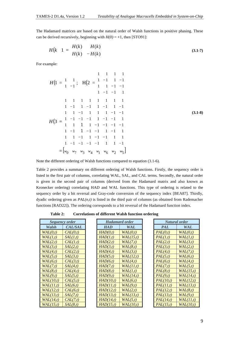
Table 2 provides a summary on different ordering of Walsh functions. Firstly, the sequency order is listed in the first pair of columns, correlating WAL, SAL, and CAL terms. Secondly, the natural order is given in the second pair of columns (derived from the Hadamard matrix and also known as Kronecker ordering) correlating HAD and WAL functions. This type of ordering is related to the sequency order by a bit reversal and Gray-code conversion of the sequency index [BEA87]. Thirdly, dyadic ordering given as PAL(n,t) is listed in the third pair of columns (as obtained from Rademacher functions [RAD22]). The ordering corresponds to a bit reversal of the Hadamard function index.
Table 2: Correlations of different Walsh function ordering
Sequency order Hadamard order Natural order Walsh CAL/SAL HAD WAL PAL WAL
WAL(0,t) CAL(0,t) HAD(0,t) WAL(0,t) PAL(0,t) WAL(0,t) WAL(1,t) SAL(1,t) HAD(1,t) WAL(15,t) PAL(1,t) WAL(1,t) WAL(2,t) CAL(1,t) HAD(2,t) WAL(7,t) PAL(2,t) WAL(3,t) WAL(3,t) SAL(2,t) HAD(3,t) WAL(8,t) PAL(3,t) WAL(2,t) WAL(4,t) CAL(2,t) HAD(4,t) WAL(3,t) PAL(4,t) WAL(7,t) WAL(5,t) SAL(3,t) HAD(5,t) WAL(12,t) PAL(5,t) WAL(6,t) WAL(6,t) CAL(3,t) HAD(6,t) WAL(4,t) PAL(6,t) WAL(4,t) WAL(7,t) SAL(4,t) HAD(7,t) WAL(11,t) PAL(7,t) WAL(5,t) WAL(8,t) CAL(4,t) HAD(8,t) WAL(1,t) PAL(8,t) WAL(15,t) WAL(9,t) SAL(5,t) HAD(9,t) WAL(14,t) PAL(9,t) WAL(14,t) WAL(10,t) CAL(5,t) HAD(10,t) WAL(6,t) PAL(10,t) WAL(12,t) WAL(11,t) SAL(6,t) HAD(11,t) WAL(9,t) PAL(11,t) WAL(13,t) WAL(12,t) CAL(6,t) HAD(12,t) WAL(2,t) PAL(12,t) WAL(8,t) WAL(13,t) SAL(7,t) HAD(13,t) WAL(13,t) PAL(13,t) WAL(9,t) WAL(14,t) CAL(7,t) HAD(14,t) WAL(5,t) PAL(14,t) WAL(11,t) WAL(15,t) SAL(8,t) HAD(15,t) WAL(10,t) PAL(15,t) WAL(10,t)

TAMES-2 D1.4a, Version 1.2 Testability of Analogue Macrocells Embedded in System-on-Chip
10
3.2 Walsh Transform An integratable function can be described in terms of Walsh functions as given in equation (3.1-3). In the finite discrete Walsh transform, the integration is replaced by summation. The coefficients, Xk, of a Walsh transform can be determined for N data points xi (N has to be a power of 2):
( ) 12,1,0 ; ,WAL1 1
0
−=⋅⋅= ∑−
=
NninxN
XN
iin K (3.2-1)
The transform can be executed by matrix manipulation as follows:
12,1,0 ; 1
−=⋅⋅= NnWxN
X kink K (3.2-2)
where Wki is the N x N transfer matrix. The coefficients depend on the type of Walsh function ordering.
3.3 Fast Walsh Transform Due to the redundancies in the Walsh transfer matrix, fast algorithms have been generated similar to the FFT analysis. While the Walsh transform given in (3.2-1) requires N2 operations, fast Walsh transforms (FWT) reduce this number to N log2N (summations / subtractions).
For the sequency ordered coefficients, defined as in (3.1-1), the following calculation can be carried out by a FWT in stages:
( ) ( ) ( )( )[ ]∏∑∑
−
=
+
=−
+−−−==1
0
11
001
1111
,WAL1 p
r iii
iinN-
in
r
p
rrrp xN
inN
X K (3.3-1)
where xi is given as ( )01 iipx K−
, Xn as ( )01 nnpX K−
, where ir and nr are binary bits of i and n with
r = 0,1,2…p [BEA75]. Each stage in the FWT corresponds to a power of 2 (for N).
x0
x1
x2
x3
x4
x5
x6
x7
x8
x9
x10
x11
x12
x13
x14
x15
D0
D1
D2
D3
D4
D5
D6
D7
D8
D9
D10
D11
D12
D13
D14
D15
A0 B0 C0
Out
put t
rans
form
ed s
ampl
es (
in b
it re
vert
ed s
eque
ncy
orde
r)
Inpu
t sig
nal s
ampl
es (
time
hist
ory)
Figure 5: Signal flow diagram for FWT (sequency ordered, Larsen’s FWT) [BEA75]
TAMES-2 D1.4a, Version 1.2 Testability of Analogue Macrocells Embedded in System-on-Chip
11
For clarification and to evaluate area efficient concepts for on-chip FWT calculation, an example shall be given here for a 16 data point transform. This can be explained best, using a signal flow diagram, where the nodes correspond to variables, solid lines carry the input variable maintaining its sign, and dashed lines indicate a change in the input variable’s sign for the addition to be carried out. Concentration is placed on butterfly structures, which have an inherent advantage in terms of memory requirements. Figure 5 illustrates the flow diagram for a 16-point Walsh Butterfly algorithm where dashed lines indicate a change in sign for the addition. It is important to notice that results D0 to D15 are provided in bit-reversed order. Note that any stage’s computations only require the previous stage’s outputs, which means that new results can overwrite the stored previous stage’s output values. This will is discussed further in section 3.9. Other flow diagrams can be generated for direct application of the sequency ordered Walsh transform, where results are ordered in sequency. The interested reader is referred to [BEA75, BEA87] for further details.
3.4 Power Calculation from FWT Results The results of a Walsh transform can vary considerably when the same waveform is analysed for different phase shifts. However, complementary effects have been identified on a pair of SAL and CAL coefficients. The phase shift is less important for the sum of squares of SAL and CAL terms [BEA75]. Obviously the effect of the phase shift is not of importance, where a signal is analysed with a fixed reference (such as the rising edge of a pulse waveform).
The spectral analysis using Walsh transforms is currently based on the use of the following definition for Walsh power coefficients, P(k):
22 |),(||),(| tkSALtkCALPk += where
),2/()2/(
12/,,.........2,1for ),(),()(
)0()0(
2
22
2
tNXNP
NktkXtkXkP
XP
S
SC
C
=
−=+=
=
(3.4-1)
Where CAL and SAL are the Walsh functions listed in Table 2. Note that the equations above can represent the energy, the square root of P(k) does not give a sequency amplitude spectrum as it can be obtained for the Fourier transform.
3.5 Example Synthesis using Walsh and Fourier Series The following examples illustrate some typical examples of waveform synthesis using Walsh and Fourier series. Figure 6 illustrates Walsh and Fourier synthesis of a continuous waveform. The Walsh synthesis requires about twice as many terms as the Fourier synthesis to achieve similar accuracy. For a discontinuous waveform (bearing similarity to a bit-stream), Walsh synthesis requires less terms and matches the original waveform more accurately, as illustrated in Figure 7.

TAMES-2 D1.4a, Version 1.2 Testability of Analogue Macrocells Embedded in System-on-Chip
12
Original waveform
Fourier 134 terms
Walsh 131 terms Walsh 244 terms
Fourier 87 terms
Figure 6: Synthesis of continuous seismic waveform [BEA75]
Original waveform
Walsh 24 terms
Fourier 18 terms
Fourier 44 terms
Figure 7: Synthesis of rectangular waveform [BEA75]
3.6 Walsh Transform Example For an input data sequence of xn = (1, 2, 0, 3), the Walsh transform for the N = 4 data points uses a 4 x 4 transform matrix Wki. Using the first four rows of the Walsh functions in sequency order and positive phasing, the transformation results to:
[ ]
[ ] [ ]15.005.1420641
111111111111
1111
302141
−=−=
−−−−
−−⋅⋅=kX
(3.6-1)
TAMES-2 D1.4a, Version 1.2 Testability of Analogue Macrocells Embedded in System-on-Chip
13
The power spectrum can be calculated with power components given (3.4-1), this results to:
( ) 11)2(
0.250.50)1(
25.25.1)0(
2
22
2
=−=
=+=
==
P
P
P
(3.6-2)
3.7 Walsh Test Solution Compared to FFT transforms, the time required to process the data collected can be significantly reduced using the Walsh transform for discontinuous type of waveforms. That is due to the more simplistic calculations needed to carry out the analysis.
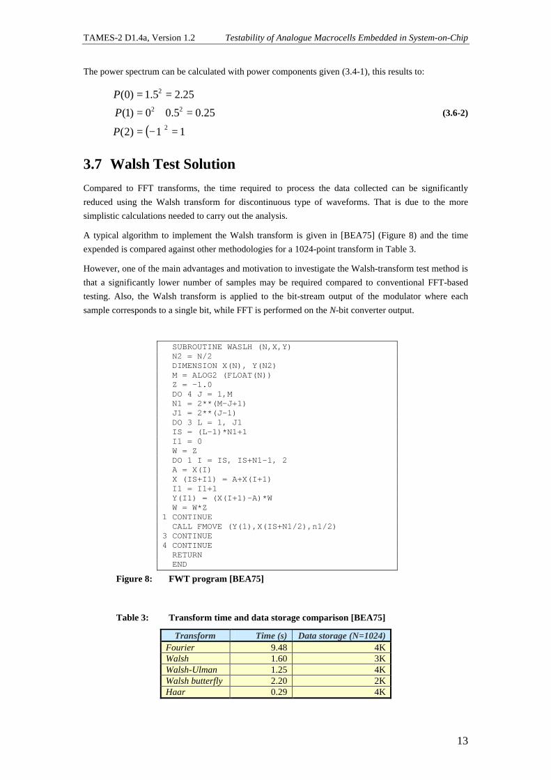
A typical algorithm to implement the Walsh transform is given in [BEA75] (Figure 8) and the time expended is compared against other methodologies for a 1024-point transform in Table 3.
However, one of the main advantages and motivation to investigate the Walsh-transform test method is that a significantly lower number of samples may be required compared to conventional FFT-based testing. Also, the Walsh transform is applied to the bit-stream output of the modulator where each sample corresponds to a single bit, while FFT is performed on the N-bit converter output.
SUBROUTINE WASLH (N,X,Y) N2 = N/2 DIMENSION X(N), Y(N2) M = ALOG2 (FLOAT(N)) Z = -1.0 DO 4 J = 1,M N1 = 2**(M-J+1) J1 = 2**(J-1) DO 3 L = 1, J1 IS = (L-1)*N1+1 I1 = 0 W = Z DO 1 I = IS, IS+N1-1, 2 A = X(I) X (IS+I1) = A+X(I+1) I1 = I1+1 Y(I1) = (X(I+1)-A)*W W = W*Z 1 CONTINUE CALL FMOVE (Y(1),X(IS+N1/2),n1/2) 3 CONTINUE 4 CONTINUE RETURN END
Figure 8: FWT program [BEA75]
Table 3: Transform time and data storage comparison [BEA75]
Transform Time (s) Data storage (N=1024) Fourier 9.48 4K Walsh 1.60 3K Walsh-Ulman 1.25 4K Walsh butterfly 2.20 2K Haar 0.29 4K
TAMES-2 D1.4a, Version 1.2 Testability of Analogue Macrocells Embedded in System-on-Chip
14
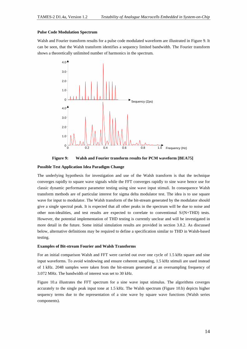
Pulse Code Modulation Spectrum
Walsh and Fourier transform results for a pulse code modulated waveform are illustrated in Figure 9. It can be seen, that the Walsh transform identifies a sequency limited bandwidth. The Fourier transform shows a theoretically unlimited number of harmonics in the spectrum.
4.0
3.0
2.0
1.0
0Sequency (Zps)
0 0.2 0.4 0.6 0.8 1.0
4.0
3.0
2.0
1.0
0Frequency (Hz)
Figure 9: Walsh and Fourier transform results for PCM waveform [BEA75]
Possible Test Application Idea Paradigm Change
The underlying hypothesis for investigation and use of the Walsh transform is that the technique converges rapidly to square wave signals while the FFT converges rapidly to sine wave hence use for classic dynamic performance parameter testing using sine wave input stimuli. In consequence Walsh transform methods are of particular interest for sigma delta modulator test. The idea is to use square wave for input to modulator. The Walsh transform of the bit-stream generated by the modulator should give a single spectral peak. It is expected that all other peaks in the spectrum will be due to noise and other non-idealities, and test results are expected to correlate to conventional S/(N+THD) tests. However, the potential implementation of THD testing is currently unclear and will be investigated in more detail in the future. Some initial simulation results are provided in section 3.8.2. As discussed below, alternative definitions may be required to define a specification similar to THD in Walsh-based testing.
Examples of Bit-stream Fourier and Walsh Transforms
For an initial comparison Walsh and FFT were carried out over one cycle of 1.5 kHz square and sine input waveforms. To avoid windowing and ensure coherent sampling, 1.5 kHz stimuli are used instead of 1 kHz. 2048 samples were taken from the bit-stream generated at an oversampling frequency of 3.072 MHz. The bandwidth of interest was set to 30 kHz.
Figure 10.a illustrates the FFT spectrum for a sine wave input stimulus. The algorithms coverges accurately to the single peak input tone at 1.5 kHz. The Walsh spectrum (Figure 10.b) depicts higher sequency terms due to the representation of a sine wave by square wave functions (Walsh series components).

TAMES-2 D1.4a, Version 1.2 Testability of Analogue Macrocells Embedded in System-on-Chip
15
(a)0 0.5 1 1.5 2 2.5 3
x 104
0
0.02
0.04
0.06
0.08
0.1
0.12
0.14Magnitude of F(k) for bitstream
Hertz
|f(k)
(b)0 0.5 1 1.5 2 2.5 3
x 104
0
0.02
0.04
0.06
0.08
0.1
0.12Plot of Walsh Ordered Coefficients for Bit stream
Sequency
Pow
er S
pect
rum
Figure 10: FFT and Walsh results on modulator bit-stream with sine wave input
For the square wave input, the FFT spectrum (Figure 11.a) contains higher frequency terms due to the representation of the square wave by sine wave components. The Walsh spectrum (Figure 11.b), on the other hand, shows a single sequency peak.
(a) 0 0.5 1 1.5 2 2.5 3
x 104
0
0.01
0.02
0.03
0.04
0.05
0.06
0.07Magnitude of F(k) for bitstream of 1.5KHz square wave
Hertz
|f(k)
(b) 0 0.5 1 1.5 2 2.5 3
x 104
0
0.005
0.01
0.015
0.02
0.025
0.03
0.035
0.04
0.045Plot of Walsh spectrum for Bit stream of 1.5KHz square wave
Sequency
Pow
er S
pect
rum
mag
nitu
de
Figure 11: FFT and Walsh results on modulator bit-stream with square wave input
Possible Advantages and Disadvantages
The main expected advantages are associated to the expected lower number of samples required for the Walsh transform due to better convergence to the bit stream output. Additionally the calculation in the transform itself are simpler than for FFT, which makes it more feasible for on-chip processing. These calculations replace multiplication and accumulation by additions and subtractions.
The main disadvantages can be seen in the fact that Walsh analyses do not converge to sinusoidal waveforms as well as Fourier analyses. As dynamic performance parameters are defined for sine wave input signals, some alternative definition of correlated performance parameters may be required when square wave input stimuli are used for Walsh analyses. Future work may use mean square error approximations as an initial analysis tool (metric) to more formally compare Walsh results against FFT results.
While the work documented in this section of the deliverable mainly concerns the evaluation of the Walsh transform test using square wave input stimuli, other related square waves transforms, hybrid transforms, and faster sine-based transforms may be of interest in future work (such as Haar, Slant, discrete wavelet transforms, discrete cosine transforms and such like.

TAMES-2 D1.4a, Version 1.2 Testability of Analogue Macrocells Embedded in System-on-Chip
16
3.8 Assessment of Applicability and Test Coverage The motivation for the simulation work documented in this section is to determine the specification testing effectiveness of the Walsh transform test. As documented in deliverable D1.2 [TAM04], modulator behaviour and model parameters that lead to performance failure in the FFT domain have been determined. Additionally, the concept for modulator performance failure models has been introduced. Here, these performance failures are investigate for Walsh-based testing, including
1. SNR deviation within specification (using modulator S/(N+THD) failure model)
2. SNR failure (using modulator S/(N+THD) failure model)
As described in D1.2, simulation results for FFT-based tests indicate that there is a relatively sharp transition from close to ideal performance (sometimes with a soft deviation) to major performance loss or even catastrophic failure. The value of failure mode parameters, such as the extend of gain deviation, have been determined around this failure mode transition.
Walsh Analysis Setup
For the simulations of the Walsh analysis a 1.5 kHz bipolar square wave input stimulus with an amplitude of 2 V is applied to the modulator. Sampling of the bit-stream (generated at 3.072 MHz) is carried out for 16384 and 65536 samples. The Walsh transform is applied to the bit-stream output (where one sample corresponds to 1 bit). The Walsh power spectrum is generated from the computed sequency.
The C-style evaluation algorithm is based on the inline fast Walsh transform (Figure 5) and includes code for the calculation of the power spectrum, SNR and THDW performance parameters. The index W at THDW is meant to indicate that a performance parameter is computed through Walsh analysis that is similar (not identical) to THD in FFT-based testing. The SNR and THDW performance parameters are determined according to:
+++⋅=
⋅=
26
23
22
2,
10
2,
2,
10
...log10)dB(
log10)dB(
HHH
rmsSW
rmsN
rmsS
VVV
VTHD
VV
SNR
(3.8-1)
where VS,rms2 is the signal power and VH<2:6> correspond to the harmonic components.
To date, no sequency limiting or filtering is applied. Further work on Walsh will address this matter.
3.8.1 Sensitivity to Input Stimulus Accuracy
The sensitivity of Walsh test results requires careful investigation in order to determine
• Test stimulus accuracy requirements
• Pass/fail thresholds for Walsh tests.

TAMES-2 D1.4a, Version 1.2 Testability of Analogue Macrocells Embedded in System-on-Chip
17
Regarding test stimulus accuracy requirements, the following characteristics of a square wave stimulus have been assessed by means of simulation (using the C++ model described in D1.2 [TAM04]):
• Rise and fall times
• Overshoot and undershoot
• Amplitude
Results are documented in this and following sections. The sensitivity of Walsh test results to noise is assessed in the next section. The test signal used in all simulations is a 1.5 kHz square wave, with a nominal amplitude of +/-2 V and 16384 samples (at 3.072 MHz) are processed in the Walsh transformation. A typical data sheet for square wave generators can offer reference values for testing the effectiveness of the Walsh technique under non-ideal circumstances.
Rise and Fall Times
A rather conservative value for finite rise and fall times specifications of a square wave generator is 20 ns (Agilent Technologies Data sheet, 33120A [AGI01]). However, note that the bit-stream is generated at 1 bit every 325 ns.
To execute coherent sampling, relations between test stimulus frequency FT, sampling frequency FS, number of samples N, and number of stimulus periods M can be given as [MAH87]:
UTP
NF
MF
S
T
1=∆
∆⋅=
∆⋅=
(3.8.1-1)
(3.8.1-2)
(3.8.1-3)
where ∆ is the so-called primitive frequency and UTP the unit test period. M and N have to have no
common divisor apart from 1. The condition of coherent sampling is then given by:
NM
FF
S
T = (3.8.1-4)
For our case, the sampling frequency is 3.072 MHz. The number of samples currently considered for Walsh transformation is 214 and 216. The primitive frequency and unit test period can be determined from equations (3.8.1-2) and (3.8.1-3). Aiming for a test stimulus frequency close to 1 kHz, parameters M and FT can be determined from (3.8.1-1) and evaluated for coherent sampling with (3.8.1-4). Values are listed in Table 4, including the effective distance D between two adjacent samples (D = (FT*N)-1) and an indication whether coherent sampling is fulfilled. These calculations reveal that for coherent sampling the distance between N samples over one period of the input waveform is well beyond or just in a similar range as the rather conservative rise/fall time specification mentioned above. This means that the rise/fall time (and similarly jitter) of the square wave test stimulus will not have any significant effect on the results of the Walsh transformation.
Table 4: Distance of samples when coherent sampling is applied (Fs = 3.072 MHz)
N ∆ (Hz) M FT (Hz) D (ns) Coherent 16384 187.50 5 937.5 65.1 Yes 16384 187.50 6 1125.0 57.3 No 65536 46.88 21 984.4 15.5 Yes 65536 46.88 22 1031.3 14.8 No
TAMES-2 D1.4a, Version 1.2 Testability of Analogue Macrocells Embedded in System-on-Chip
18
Overshoot
As above, a rather conservative stimulus accuracy is assumed for the investigation of stimulus overshoot. For the same waveform generator as above [AGI01], the overshoot is specified at 4 %. For the case of a square wave with 2 V maximum amplitude would translate to a 0.08 V deviation from the nominal value.
Regarding an overshoot present in the test stimulus waveform two main characteristics are taken into account. The first relates to the actual maximum amplitude of the overshoot, i.e. what is the tolerance level of the analysis for overshoots of different maximum amplitude. The second addresses overshoots with different damping frequencies. The modelling of these effects has been incorporated in the same C-style model for the complete modulator structure. However, a slight inflexibility in the modelling for the overshoot effect has imposed a small restrain on the rate at which different cases could be simulated. Nevertheless, the analysis has been executed successfully and some representative cases have been accounted for, out of which two are included in Table 5.
Simulation results show that the Walsh analysis is relatively insensitive to the considered overshoot effects. The ideal SNR is 97.6 dB for 16384 samples, and an overshoot well beyond the conservative waveform generator specification mentioned above leads to a mere maximum drop of 3 dB in the SNR. Furthermore, the Walsh analysis appears to be relatively insensitive to long damping times. A damping time of 0.14 ms accounts for one fourth of the pulse time leads to a small degradation in SNR.
Table 5: Effect of overshoot on Walsh analysis
Overshoot Damping (ms) SNR (dB) Ideal - 97.6
0.06 94.7 Max. amplitude of 2.05 V 0.14 95.9 0.06 94.6 Max. amplitude of 2.15 V 0.14 95.5
Further work on the stimulus accuracy requirements will include an analysis of undershoot effects, degradation in square wave amplitude over the pulse duration, and impact of asymmetry in the square wave signal. The effect of different square wave amplitudes on the Walsh analysis is included in the next section.
3.8.2 Coverage Against Performance Parameter Failure
This section presents results obtained by employing the Walsh technique for the analysis of the fourth order sigma-delta modulator. The modulator performance assessment has been mainly implemented for the following different cases:
• Analysis of optimum stimulus amplitude and effect of number of samples
• Analysis of “robustness” of the Walsh test technique for noise affected input stimuli for ideal, fault free devices.
• Determination of thresholds for SNR tests through Walsh analysis.
• Effect of stimulus accuracy on SNR tests through Walsh analysis.

TAMES-2 D1.4a, Version 1.2 Testability of Analogue Macrocells Embedded in System-on-Chip
19
To assess the impact of noise on Walsh test results, a noise signal has been added to the input stimulus analogously to the investigation of noise impact on FFT-based testing (D1.2). In FFT-based testing, the following stimulus was used within the C++ modulator model:
( ) ( ) ( )randdoublektDClevelPIMin ⋅+⋅⋅⋅⋅= _0.2sin5.2 (3.8.2-1)
where the first term correlates to the input sine-wave component of 2.5 V amplitude while the second term models the noise portion of the integrator input. The parameter k can be varied to model different noise levels. For the Walsh-based test, the following input stimulus is used:
( ) ( )randdoubleksquarewavein ⋅+= (3.8.2-2)
The effect of square wave stimulus amplitude and number of samples transformed by Walsh is summarised in Table 6 for the ideal case (without significant noise contribution). Obviously the SNR improves with increasing stimulus power until the modulator is driven into saturation causing catastrophic malfunction. Similarly, when more samples are taken into account in the Walsh transformation, the computed SNR improves. Figure 12 illustrates the Walsh power spectrum for a 2 V input stimulus amplitude for 16384 and 65536 samples. For the higher resolution spectrum, the noise floor is appears lower over the entire sequency range. Further work will investigate even higher number of samples and determine accuracies achieved for different numbers of samples in Walsh-based SNR tests.
Table 6: Effect of square wave amplitude on Walsh power spectrum and specifications
Square wave amplitude (V) # samples SNR (dB) 1.9 93.9 2.0 94.8 2.1 93.6 2.2 96.23 2.3
16384
9.73 1.9 104.4 2.0 107.57 2.1 102.46 2.2 107.68 2.3
65536
3.41
SMASH 4.4.0 - Generic - Wed Mar 10 21:51:27 2004
WALLOGWALLOG
2K 4K 6K 8K 10K 12K 14K 16K 18K 20K 22K 24K 26K 28K
-170
-160
-150
-140
-130
-120
-110
-100
-90
-80
-70
-60
-50
-40
-30
-20
-10
0
10
Figure 12: Walsh power spectrum for 214 and 216 samples (2.0 V amplitude)

TAMES-2 D1.4a, Version 1.2 Testability of Analogue Macrocells Embedded in System-on-Chip
20
Effect of noise on Walsh power spectrum for SNR testing
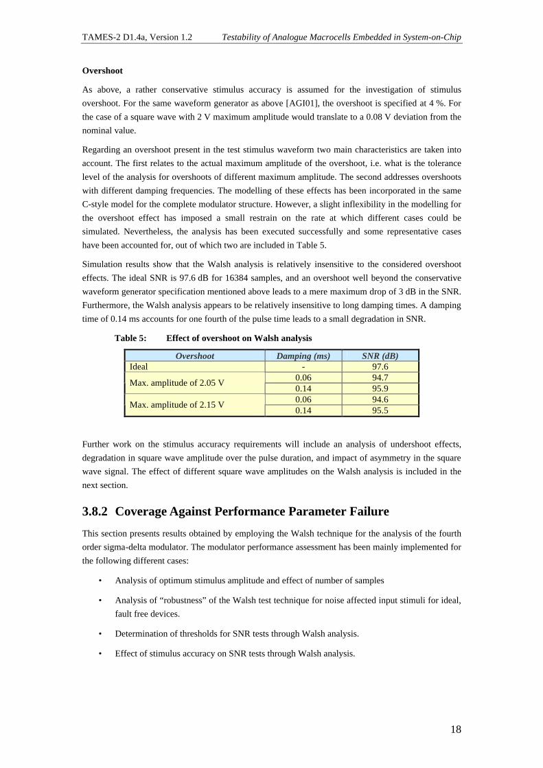
The aim of this analysis is to provide evidence for SNR specification testing effectiveness of the Walsh analysis. Simulation of the Walsh test method have been conducted for different square wave amplitudes and two different number of samples. A summary of the results is given in Table 7 and graphical representation of data is provided in Figure 13.
The most significant difference between the Walsh SNR measurements and S/(N+THD) measurements by FFT-analysis is that the SNR computed by Walsh remains almost constant with increasing noise levels until some threshold value is reached. Thereafter the Walsh transform results indicate catastrophic failure in SNR with the corresponding Walsh power spectrum illustrated in Figure 14. While no major changes can be seen in the Walsh power spectrum before that transition to failure, beyond the transition the entire noise floor is affected significantly and exhibits what appears similar to harmonic tones in FFT-analysis. However, the interpretation of this effect requires further investigation.
Additionally, this transition point seems to be independent from the stimulus amplitude. The transition point can be seen for the analysis of 216 samples in Figure 13. For 214 samples, this transition point to catastrophic SNR failure occurs for a maximum noise amplitude beyond 30 mV.
When the Walsh transform is applied to a higher number of samples, the ideal SNR increases which could be due to an averaging of noise or the inability to accurately describe the bit-stream output in terms of Walsh functions. However, FFT-analyses behave in similar ways when the number of samples is reduced.
Even though these simulation results indicate some potential for SNR test by Walsh-analysis, the full reasoning behind the sharp performance parameter transition is not yet fully understood. Further work is required, to determine the actual cause of this effect, that could also lie within the computation of the SNR value in the Walsh algorithm. Also, the effect of further increase in the number of samples will be investigated in order to determine the exact number of samples required for Walsh-based SNR testing. Further future work is outlined and discussed in section 3.10.
Table 7: Preliminary results on SNR testing through Walsh analysis
Case Stimulus ampl. (V)
Modelling of noise contribution
Max. noise ampl. (V)
SNR (dB) Remark
(1.0e-14*(double)rand()) 3.2767E-10 101.3 Ideal (1.0e-8*(double)rand()) 3.2767E-04 100 (3.0e-8*(double)rand()) 9.8301E-04 96 (6.0e-8*(double)rand()) 1.9660E-03 91.3
FFT 2.5
(1.0e-7*(double)rand()) 3.2767E-03 87.2 (1.0e-14*(double)rand()) 3.2767E-10 94.8 2.0
(1.0e-7*(double)rand()) 3.2767E-03 94.6 (1.0e-14*(double)rand()) 3.2767E-10 93.6 2.1
(1.0e-7*(double)rand()) 3.2767E-03 94.2 (1.0e-14*(double)rand()) 3.2767E-10 96.2
Walsh (N=214)
2.2 (1.0e-7*(double)rand()) 3.2767E-03 100.2
Failure beyond 30 mV max. noise
amplitude
(1.0e-14*(double)rand()) 3.2767E-10 102.4 (4.0e-11*(double)rand()) 1.3107E-06 102.4 2.1 (5.0e-11*(double)rand()) 1.6384E-06 27.3 Failure (1.0e-14*(double)rand()) 3.2767E-10 107.6 (4.0e-11*(double)rand()) 1.3107E-06 107.6
Walsh (N=216)
2.2 (5.0e-11*(double)rand()) 1.6384E-06 30.4 Failure
TAMES-2 D1.4a, Version 1.2 Testability of Analogue Macrocells Embedded in System-on-Chip
21
50
60
70
80
90
100
110
1.0E-08 1.0E-07 1.0E-06 1.0E-05 1.0E-04 1.0E-03 1.0E-02Maximum noise amplitude (V)
SN
R (
dB
)
FFT 2.5 V
Walsh,N=2^12, 2.0 V
Walsh,N=2^12, 2.1 V
Walsh,N=2^12, 2.2 V
Walsh,N=2^14, 2.1 V
Walsh,N=2^14, 2.2 V
Transition for 216 samples
Figure 13: SNR through Walsh – preliminary simulation results
SMASH 4.4.0 - Generic - Thu Mar 11 22:26:27 2004
WALLOGWALLOG
x = 5.393K, dx = 7.319K, y = -13.24, dy = -31.6, period = 136.6u, slope = -0.004322K 4K 6K 8K 10K 12K 14K 16K 18K 20K 22K 24K 26K 28K
-150
-140
-130
-120
-110
-100
-90
-80
-70
-60
-50
-40
-30
-20
-10
failure
ideal
Figure 14: Walsh power spectrum for failure in SNR (preliminary results)
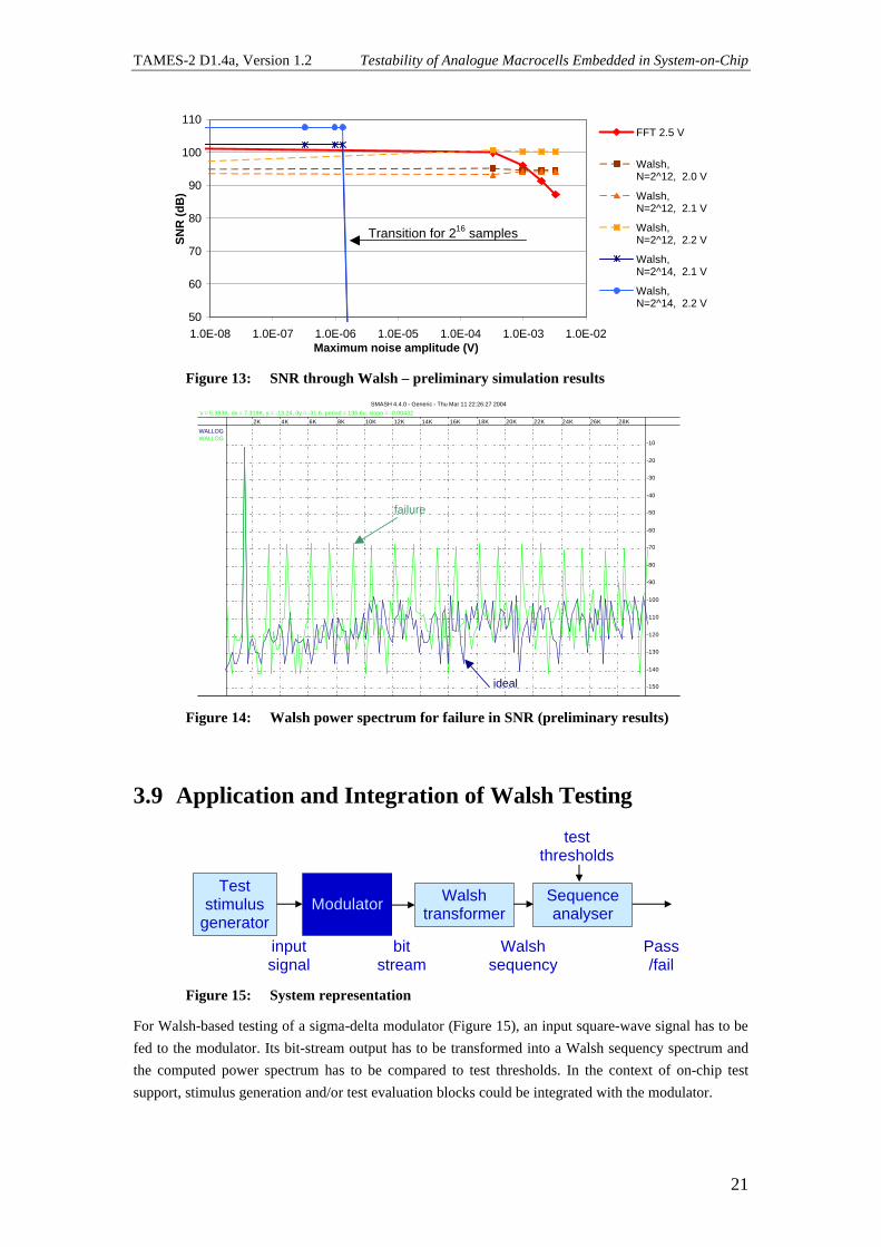
3.9 Application and Integration of Walsh Testing
Test stimulus
generator
Walsh transformer
Modulator
input signal
bit stream
Sequence analyser
Walsh sequency
test thresholds
Pass /fail
Figure 15: System representation
For Walsh-based testing of a sigma-delta modulator (Figure 15), an input square-wave signal has to be fed to the modulator. Its bit-stream output has to be transformed into a Walsh sequency spectrum and the computed power spectrum has to be compared to test thresholds. In the context of on-chip test support, stimulus generation and/or test evaluation blocks could be integrated with the modulator.
TAMES-2 D1.4a, Version 1.2 Testability of Analogue Macrocells Embedded in System-on-Chip
22
For external Walsh-based testing, the test evaluation algorithms described in section 3.2 to 3.4 can be executed off-chip if access to the bit-stream is provided. Access to the modulator input is obviously also required when the test stimulus is generated externally.
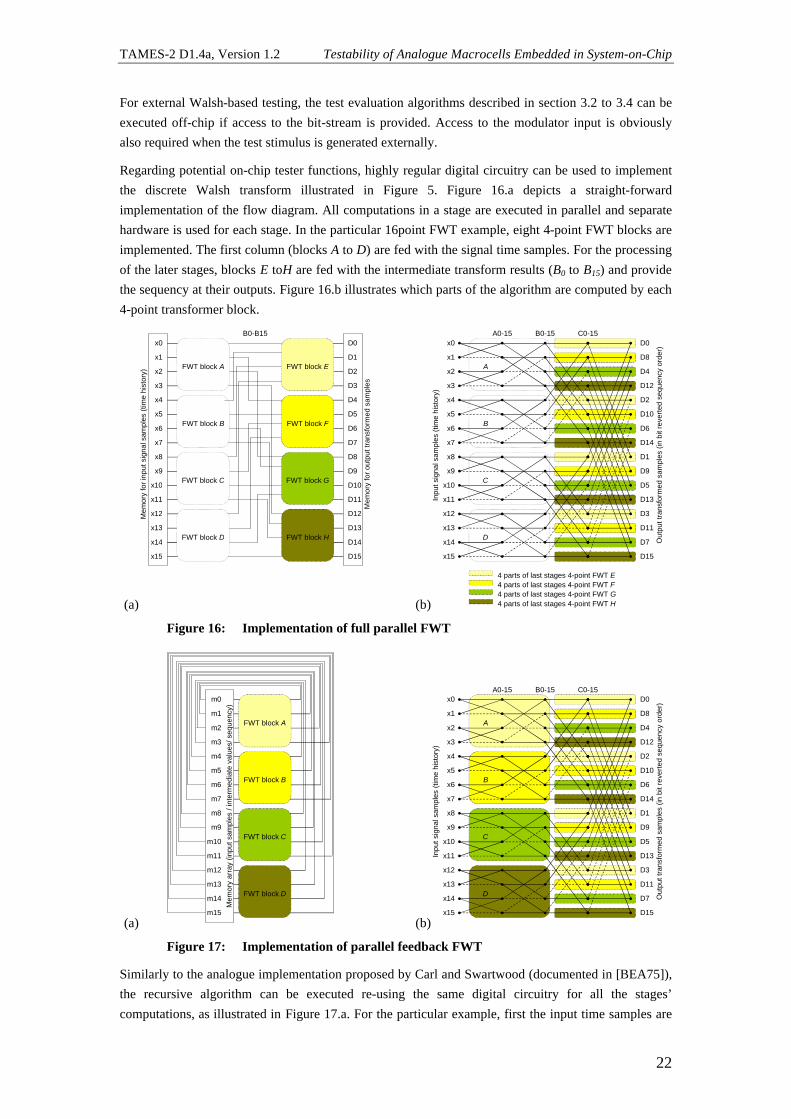
Regarding potential on-chip tester functions, highly regular digital circuitry can be used to implement the discrete Walsh transform illustrated in Figure 5. Figure 16.a depicts a straight-forward implementation of the flow diagram. All computations in a stage are executed in parallel and separate hardware is used for each stage. In the particular 16point FWT example, eight 4-point FWT blocks are implemented. The first column (blocks A to D) are fed with the signal time samples. For the processing of the later stages, blocks E toH are fed with the intermediate transform results (B0 to B15) and provide the sequency at their outputs. Figure 16.b illustrates which parts of the algorithm are computed by each 4-point transformer block.
(a)
x0
x1
x2
x3
x4
x5
x6
x7
x8
x9
x10
x11
x12
x13
x14
x15
D0
D8
D4
D12
D2
D10
D6
D14
D1
D9
D5
D13
D3
D11
D7
D15
B0-B15
Mem
ory
for
outp
ut tr
ansf
orm
ed s
ampl
es
Mem
ory
for
inpu
t sig
nal s
ampl
es (
time
hist
ory)
FWT block A
FWT block B
FWT block C
FWT block D
FWT block E
FWT block F
FWT block G
FWT block H
(b)
x0
x1
x2
x3
x4
x5
x6
x7
x8
x9
x10
x11
x12
x13
x14
x15
D0
D1
D2
D3
D4
D5
D6
D7
D8
D9
D10
D11
D12
D13
D14
D15
A0-15 B0-15 C0-15
Out
put t
rans
form
ed s
ampl
es (
in b
it re
vert
ed s
eque
ncy
orde
r)
Inpu
t sig
nal s
ampl
es (t
ime
hist
ory)
4 parts of last stages 4-point FWT E 4 parts of last stages 4-point FWT F 4 parts of last stages 4-point FWT G 4 parts of last stages 4-point FWT H
A
B
C
D
Figure 16: Implementation of full parallel FWT
(a)
FWT block A
FWT block B
FWT block C
FWT block D
m0
m1
m2
m3
m4
m5
m6
m7
m8
m9
m10
m11
m12
m13
m14
m15
Mem
ory
arra
y (in
put s
ampl
es /
inte
rmed
iate
val
ues/
seq
uenc
y)
(b)
x0
x1
x2
x3
x4
x5
x6
x7
x8
x9
x10
x11
x12
x13
x14
x15
D0
D1
D2
D3
D4
D5
D6
D7
D8
D9
D10
D11
D12
D13
D14
D15
A0-15 B0-15 C0-15
Out
put t
rans
form
ed s
ampl
es (
in b
it re
vert
ed s
eque
ncy
orde
r)
Inpu
t sig
nal s
ampl
es (
time
hist
ory)
A
B
C
D
Figure 17: Implementation of parallel feedback FWT
Similarly to the analogue implementation proposed by Carl and Swartwood (documented in [BEA75]), the recursive algorithm can be executed re-using the same digital circuitry for all the stages’ computations, as illustrated in Figure 17.a. For the particular example, first the input time samples are

TAMES-2 D1.4a, Version 1.2 Testability of Analogue Macrocells Embedded in System-on-Chip
23
loaded into the memory array. The four 4-point FWT blocks then compute front-end two transform stages (Figure 17.b). Intermediate results (B0 to B15) are loaded into the memory array overwriting the original input data. The same four FWT blocks are reused to compute the last stages of the transform and sequency results can be stored in the memory array.
For a potential on-chip implementation, the hardware can be further reduced reusing circuitry for the computations within each stage. For an N-point FWT, where N is a product of integers M and K for example, hardware can be designed to execute M-point and K-point FWTs. The concept achieves largest benefit in terms of expected area overhead, where N is a power M. This is illustrated in Figure 18.a for N = 16 with M=4. One circuit that computes a 4-point FWT can be implemented and reused eight times. For explanation, the concept has been illustrated using two memory structures composed of shift registers with some parallel inputs. The FWT can be executed as follows. Firstly the input time samples are stored in the first memory structure (m0-15). The 4-point FWT block computes first transform stages for the first four input simples and results are stored in a second memory (B3,7,11,15). To access the next four time samples, the content of memory m is shifted four times, while memory B shifts once. The 4-point FWT is computed and results are stored. When the last input time samples have been processed, data stored in memory B can be transferred to memory m, and the last stages of the transform can be computed analogously. In real implementation, the shift registers can alternatively be replaced by a RAM block (in example for 16 values) plus an address counter.
(a)
FWT block A
m0
m1
m2
m3
m4
m5
m6
m7
m8
m9
m10
m11
m12
m13
m14
m15
Mem
ory
arra
y m
(sh
ift r
egis
ter
stru
ctur
e)
SH
IFT
m
B0
B1
B2
B3
B4
B5
B6
B7
B8
B9
B10
B11
B12
B13
B14
B15
Mem
ory
arra
y B
(sh
ift r
egis
ter
stru
ctur
e)
SH
IFT
B
(b)
1st
2nd
3rd
4th
5th
6th
7th
8th
5th
6th
7th
8th
5th
6th
7th
8th
5th
6th
7th
8th
x0
x1
x2
x3
x4
x5
x6
x7
x8
x9
x10
x11
x12
x13
x14
x15
D0
D1
D2
D3
D4
D5
D6
D7
D8
D9
D10
D11
D12
D13
D14
D15
A0-15 B0-15 C0-15
Out
put t
rans
form
ed s
ampl
es (
in b
it re
vert
ed s
eque
ncy
orde
r)
Inpu
t sig
nal s
ampl
es (
time
hist
ory)
Figure 18: Implementation of serial feedback FWT
Obviously, the concepts above can be expanded for more realistic FWT algorithms with a significantly higher number of input time samples and therefore higher number of transform stages. Combinations of parallel and serial transform stages can be used and the granularity of partial FWT blocks can vary.
When this technique is applied to a sigma-delta modulator to evaluate the bit-stream output, it is important to notice that the front-end input data consists of N 1-bit time samples. However, intermediate values (A0-(N-1), B0-(N-1),…) increase in size by one bit per transform stage. With N = 2p, this means that the computed sequency contains N values of (p+1) bits. In other words, it may prove more feasible to implement separate FWT blocks for computation of front-end calculations and back-end transform computation due to a significant increase in data size. One can also imagine, that more complex back-end FWT blocks can be reconfigured into multiple smaller front-end FWT blocks maintain high reuse.
TAMES-2 D1.4a, Version 1.2 Testability of Analogue Macrocells Embedded in System-on-Chip
24
Another fact to account for is that the input samples are processed in order of time in the front-end FWT. This means, that these stages can be processed as soon as a sufficient number of input samples is available. Furthermore the number of separate Walsh tests to evaluate has an impact on the best on-chip implementation. If only one test requires evaluation, transformer block reuse across the transformation stages is most promising. However, if a larger number of tests is executed and evaluated, it can be advantageous to implement separate transformer blocks in the transformation chain.
For a 16-point FWT, for example, a 4-point transformer block A may be implemented for computation of the first two stages (reused four times), while a second 4-point transformer block B is implemented for the final two stages of the transform computation. Additionally, more storage has to be implemented. This will allow continuous evaluation of a set of Walsh tests. For the 16-point example, let us assume a set of 2 Walsh tests. When the bit-stream modulator output of the first test is available for the FWT, the computation of the first couple of transform stages can be executed by block A. As soon as the intermediate results are obtained for the first test, these are stored for the final couple of FWT stages by block B. At the same time, block A can be used to perform the next FWT for the second Walsh test, and so on.
Generally, a trade-off has to be found with regard to the area overhead (decreasing with increasing circuitry reuse) and the computation time (increasing with increasing reuse). However, it may be mentioned here that the bit-stream is provided at 3.07 MHz while the clock frequency for digital circuitry will be significantly higher. A full parallel FWT (Figure 16) will lead to excessive area overhead. As an indication, in [ALA01] a FWT is implemented in an FPGA to process a 1024-point FWT. The design uses the butterfly structure with two stages of multiple 32-point FWT blocks. Including additional memory and a control unit, the circuitry is approximated to 246k gates.
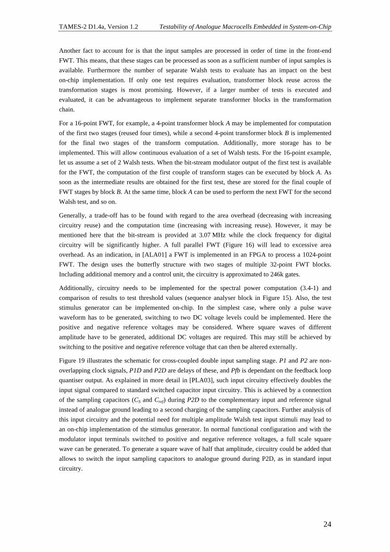
Additionally, circuitry needs to be implemented for the spectral power computation (3.4-1) and comparison of results to test threshold values (sequence analyser block in Figure 15). Also, the test stimulus generator can be implemented on-chip. In the simplest case, where only a pulse wave waveform has to be generated, switching to two DC voltage levels could be implemented. Here the positive and negative reference voltages may be considered. Where square waves of different amplitude have to be generated, additional DC voltages are required. This may still be achieved by switching to the positive and negative reference voltage that can then be altered externally.
Figure 19 illustrates the schematic for cross-coupled double input sampling stage. P1 and P2 are non-overlapping clock signals, P1D and P2D are delays of these, and Pfb is dependant on the feedback loop quantiser output. As explained in more detail in [PLA03], such input circuitry effectively doubles the input signal compared to standard switched capacitor input circuitry. This is achieved by a connection of the sampling capacitors (CS and Cref) during P2D to the complementary input and reference signal instead of analogue ground leading to a second charging of the sampling capacitors. Further analysis of this input circuitry and the potential need for multiple amplitude Walsh test input stimuli may lead to an on-chip implementation of the stimulus generator. In normal functional configuration and with the modulator input terminals switched to positive and negative reference voltages, a full scale square wave can be generated. To generate a square wave of half that amplitude, circuitry could be added that allows to switch the input sampling capacitors to analogue ground during P2D, as in standard input circuitry.
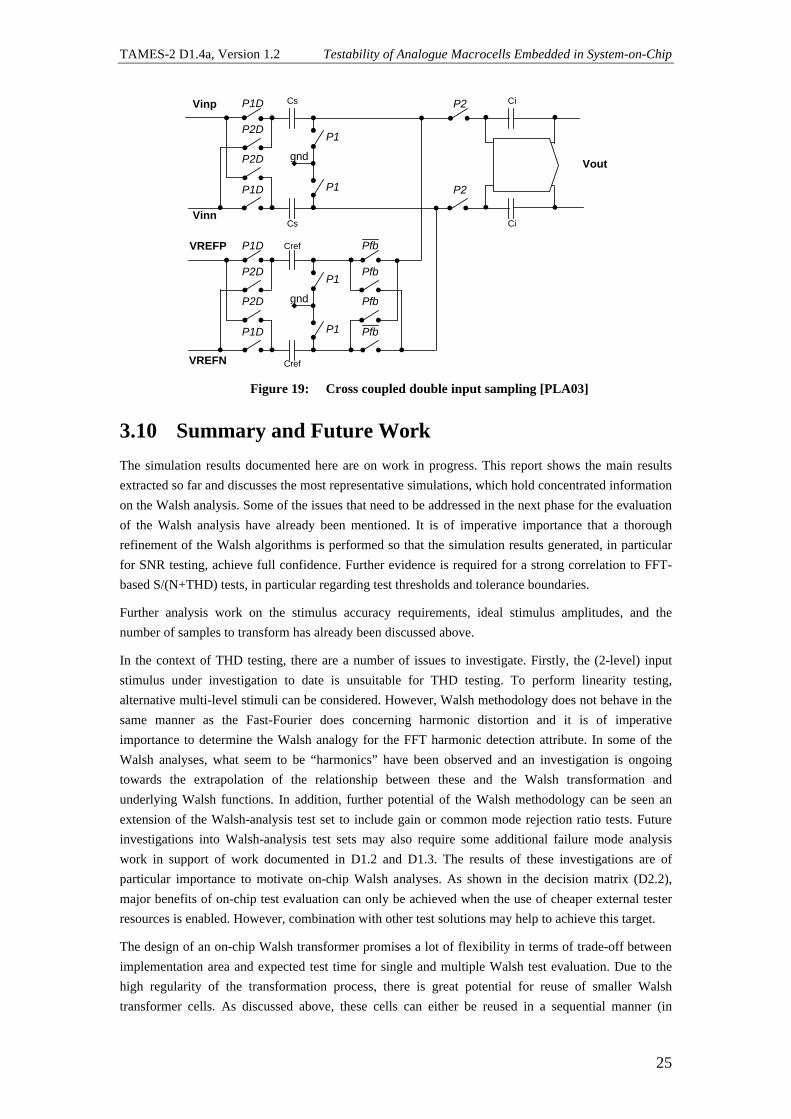
TAMES-2 D1.4a, Version 1.2 Testability of Analogue Macrocells Embedded in System-on-Chip
25
VREFP P1D
P1D
P2D
P2D
gnd
P1
P1
Pfb
Pfb
Pfb
Pfb
P2
P2
Cs
Cs
Cref
Cref
Ci
Ci
VREFN
Vinp
Vinn
Vout
P1D
P1D
P2D
P2D
gnd
P1
P1
Figure 19: Cross coupled double input sampling [PLA03]
3.10 Summary and Future Work The simulation results documented here are on work in progress. This report shows the main results extracted so far and discusses the most representative simulations, which hold concentrated information on the Walsh analysis. Some of the issues that need to be addressed in the next phase for the evaluation of the Walsh analysis have already been mentioned. It is of imperative importance that a thorough refinement of the Walsh algorithms is performed so that the simulation results generated, in particular for SNR testing, achieve full confidence. Further evidence is required for a strong correlation to FFT-based S/(N+THD) tests, in particular regarding test thresholds and tolerance boundaries.
Further analysis work on the stimulus accuracy requirements, ideal stimulus amplitudes, and the number of samples to transform has already been discussed above.
In the context of THD testing, there are a number of issues to investigate. Firstly, the (2-level) input stimulus under investigation to date is unsuitable for THD testing. To perform linearity testing, alternative multi-level stimuli can be considered. However, Walsh methodology does not behave in the same manner as the Fast-Fourier does concerning harmonic distortion and it is of imperative importance to determine the Walsh analogy for the FFT harmonic detection attribute. In some of the Walsh analyses, what seem to be “harmonics” have been observed and an investigation is ongoing towards the extrapolation of the relationship between these and the Walsh transformation and underlying Walsh functions. In addition, further potential of the Walsh methodology can be seen an extension of the Walsh-analysis test set to include gain or common mode rejection ratio tests. Future investigations into Walsh-analysis test sets may also require some additional failure mode analysis work in support of work documented in D1.2 and D1.3. The results of these investigations are of particular importance to motivate on-chip Walsh analyses. As shown in the decision matrix (D2.2), major benefits of on-chip test evaluation can only be achieved when the use of cheaper external tester resources is enabled. However, combination with other test solutions may help to achieve this target.
The design of an on-chip Walsh transformer promises a lot of flexibility in terms of trade-off between implementation area and expected test time for single and multiple Walsh test evaluation. Due to the high regularity of the transformation process, there is great potential for reuse of smaller Walsh transformer cells. As discussed above, these cells can either be reused in a sequential manner (in

TAMES-2 D1.4a, Version 1.2 Testability of Analogue Macrocells Embedded in System-on-Chip
26
different stages of the transformation) or even within separate stages. Design effort is further reduced, as basic 2 or 4-point transformer cells can be reused in more complex transformer blocks. However, the number of samples to be transformed will have a major impact on expected area overhead.
In the wider context of using alternative transforms to replace FFT-based testing, other transform methods, such as Ulman’s R transform, the Haar transform, or Slant transform, do exist for square wave signal analysis. Also with regard to transform algorithms, a range of techniques exist that do have to be analysed for their major advantages and disadvantages compared to the butterfly structure presented above.

TAMES-2 D1.4a, Version 1.2 Testability of Analogue Macrocells Embedded in System-on-Chip
27
4 Distortion Meter Method A full-scale sine signal is applied at the input of the ADC under test. The output signal containing distortion and noise riding over the high amplitude input signal is passed through a notch filter to remove the fundamental frequency. Only distortion and noise (and offset) remains at the output of the filter. This test solution is simulated with C language. The functional blocs are shown on
S? ADC Modulator + decimator
Fir3_out e
Notch1 filter
Fnotch Noise+harmonics Notch2
filter
Fnotch
C description
Notch1_out Notch2_out
Figure 20: Functional description of the distortion meter method
The behavioural simulation is plotted on Figure 22. We can see clearly the two notches settling time, which stabilize to the noise floor level at 10 ms.
SMASH 5.1.3b4 - Generic - Wed Dec 10 15:07:26 2003
e
Fir3_out
Notch1_out
Notch2_out
0 1m 2m 3m 4m 5m 6m 7m 8m 9m
-100m-50m050m100m
-40m-20m020m40m
-30m-20m-10m010m
-20m
-10m
0
Figure 21: Behavioural simulation result. E is the input signal, Fir3_out is the reconstruction of the ADC output and Notch2_out is the output of the second notch
As a consequence of the settling time, we must wait 10 ms before computing the power contained in the output signal.
For the computation of the power, we are using a sliding window containing 8 periods of Fin = 918.54 Hz signal. The equivalent number of points at 44.1 kHz is 384. The model used is "perfectly ideal". This model does not generate harmonic and noise. Harmonic components and noise are added directly to the input stimulus.

TAMES-2 D1.4a, Version 1.2 Testability of Analogue Macrocells Embedded in System-on-Chip
28
The following results show the SNR computed with the reference FFT and with the distortion meter for comparison. The signal power is first computed at the decimation filter output (Fir3_out) before the notch filter and then the noise power at the notch output (Notch2_out).
In this case, no harmonics are added on the signal. Only noise is added to input signal. The noise level is set 95 dB lower than the input signal power.
The following table show that FFT and Distortion Meter results match very well.
Table 8: Comparison of SNR measurements with FFT and Notch
Signal power FIR3_out (mVrms)
Noise Notch2_out
(µVrms)
SNR Distortion meter
(dB)
SNR FFT (dB)
281.3 4.675 95.6 95.0 281.3 4.746 95.5 95.6 281.3 4.394 95.1 95.4 281.3 4.652 95.6 95.1 281.3 4.424 96.1 94.9 281.3 3.968 97.0 95.2
The next following results show the THD computed with the reference FFT and with the distortion meter. The harmonic level is set 90 dB lower than the input signal power and noise level is set 95 dB lower than the input signal power. Again, the FFT and Distortion Meter results match very well.
Table 9: Comparison of THD measurements with FFT and Notch
Signal power FIR3_out (mVrms)
Noise Notch2_out
(µVrms)
THD Distortion meter
(dB)
THD FFT (dB)
281.3 9.399 89.52 89.5 281.3 9.302 89.61 89.4 281.3 9.415 89.51 89.4 281.3 9.418 89.50 89.2
In the real life, harmonic power may be lower than the noise power. In this case, the distortion meter solution cannot extract the harmonic power alone.
What is really measurable is the THD + noise power. To get the noise alone, the input signal amplitude must be reduced in order to lower the harmonic power below the noise floor power.
The silicon area needed for the two notches is 8 kgates. If we assume a density of 40 kgates/mm², the silicon area for two notch filters is 0.25 mm². The durations for this method are detailed in deliverable D.2.2.
As a conclusion we can list the following points:
• Distortion meter is a good candidate for SNR and THD measurements under the following conditions: THD power must be higher than noise floor with full scale input signal. In this case, noise floor can be measured with a reduced amplitude input signal. If THD is lower than noise floor, distortion meter cannot compute the THD.
• Out of band noise must be filtered out prior computation. Otherwise it will be included in the SNR result. This is normally done by decimation filter.
• Input sine wave has to be high quality.

TAMES-2 D1.4a, Version 1.2 Testability of Analogue Macrocells Embedded in System-on-Chip
29
5 Noise Transfer Function Test Another considered test solution, also published by De Venuto [VEN04], is to assess the noise transfer function of the A/D converter, shown in Figure 22. This plot represents the Bode diagram representation of the gain between the output of the converter and the SUM node. In this configuration the circuit exhibits a high pass behaviour (as shown in the graph). Testing the noise transfer function does not however support verification of all specifications, but does verify that the transfer behaviour of the converter is correct. Since the frequency response is dependent on the locations of singularities of the circuit in the frequency domain, this test could significantly reduce the test time because even if an FFT had to be implemented a reduced number of points would be required making quicker to differentiate good and defective behaviour.
SMASH 4.4.0 - Small Signal C:\dolphin\smash44\examples\Mixed-Language\ADC\IDEAL\modulateurAC.nsx - Sun Oct 13 18:36:03 2002
VDB(OUT_HICOD)
f = 15.32KHz, df = 1.646KHz, rf = 1.12, y = -46.93dB, dy = 0dB, slope = 0dB/dec.100m 1 2 3 4 10 20 100 200 1K 2K 10K 100K 1MEG 10MEG 100MEG
-260dB
-240dB
-220dB
-200dB
-180dB
-160dB
-140dB
-120dB
-100dB
-80dB
-60dB
-40dB
-20dB
0dB
20dB
40dB
60dB
Figure 22: Noise transfer function of a 4th order modulator
To perform this test, by observing the noise transfer function, it is possible to inject a sine wave at the quantizer input as shown in Figure 23, at different increasing frequencies using either a PCM or multitone stimulus. It should then be possible to observe at the output of the converter and clear response due to the gain of the loop.
SUM
- 1
- 1
- 1 b - 1 - 1 - 1 - 1 - 1 - 1 - 1 - 1 c - 1 - 1 d - 1 - 1
e
- 1 - 1 a - 1 - 1 - 1IN
CLK
VR1
TEST INPUT
f g
Figure 23: New test access for a 4th order sigma-delta modulator
To prove this method, simulations have been performed using SMASH. A sine wave has been applied at the feedback summation node while a simple model for the distortion was applied inside the polynomial representation of each block or a non-linearity was introduced electrically between them. The FFT at the output of the converter detects the amount of distortion at a lower number of samples than when just measuring the specifications from stimuli injected at the input. The test signal used was again a sine wave but in order to select the suitable frequency, different possibilities were tried and different frequencies were assumed ranging from 1 kHz, 16 kHz to 22 kHz (the last one is the zeros

TAMES-2 D1.4a, Version 1.2 Testability of Analogue Macrocells Embedded in System-on-Chip
30
location of the hiCOD design). The simulations were performed first with the test signal at the SUM node and no other signal at the input, i.e. connecting the input to ground. Then the same simulations were repeated giving at the same time a signal at the SUM node and a signal at the input with different frequency. The test input node (Figure 23) is normally easily accessible since often used to compensate the internal converter leakage.
SMASH 4.4.0 - Fast Fourier Transform C:\dolphin\smash44\examples\Mixed-Language\ADC\idealadc4b.nsx - Sun Oct 13 17:42:28 2002
BH7(V(SCOMP))
BH7(V(S1))
BH7(V(S2))
f = 4.41KHz, df = 7.187KHz, y = -82.72, dy = -112.8, period = 139.1us, slope = -0.01572 K 4 K 6 K 8K 10K 1 2 K 14K 16K 18K 20K 2 2 K
-120
-100
-80
-60
-40
-20
-160
-140
-120
-100
-80
-60
-120
-100
-80
-60
-40
SMASH 4.4.0 - Fast Fourier Transform C:\dolphin\smash44\examples\Mixed-Language\ADC\idealadc4b.nsx - Sun Oct 13 11:13:31 2002
BH7(V(SCOMP))
BH7(V(S1))
BH7(V(S2))
f = 1.918KHz, df = 1.362KHz, y = -97.66, dy = -93.74, period = 734.2us, slope = -0.06882K 4K 6K 8K 10K 12K 14K 16K 18K 20K 22K
-140
-120
-100
-80
-60
-40
-140
-120
-100
-80
-60
-120
-100
-80
-60
SMASH 4.4.0 - Fast Fourier Transform C:\dolphin\smash44\examples\Mixed-Language\ADC\idealadc4b.nsx - Sun Oct 13 17:43:46 2002
BH7(V(S3))
BH7(V(S4))
f = 4.41KHz, df = 7.187KHz, y = -82.72, dy = -112.8, period = 139.1us, slope = -0.01572K 4K 6K 8K 10K 12K 14K 16K 18K 20K 22K
-120
-100
-80
-60
-40
-160
-140
-120
-100
-80
-60
-40
Figure 24: FFT at the output of the ADC, at S1, S2 S3, S4
SMASH 4.4.0 - Fast Fourier Transform C:\dolphin\smash44\examples\Mixed-Language\ADC\idealadc4b.nsx - Sun Oct 13 11:15:31 2002
BH7(V(S3))
BH7(V(S4))
f = 1.918KHz, df = 1.362KHz, y = -97.66, dy = -93.74, period = 734.2us, slope = -0.0688
2K 4K 6K 8K 10K 12K 14K 16K 18K 20K 22K
-120
-100
-80
-60
-40
-160
-120
-80
-40
Figure 25: As in Figure 24, distortion applied at the first block
SMASH 4.4.0 - Fast Fourier Transform C:\dolphin\smash44\examples\Mixed-Language\ADC\idealadc4b.nsx - Sun Oct 13 11:47:26 2002
BH7(V(SCOMP))
BH7(V(S1))
BH7(V(S2))
2K 4K 6K 8K 10K 12K 14K 16K 18K 20K 22K
-120
-100
-80
-60
-40
-20
-160
-140
-120
-100
-80
-60
-160
-120
-80
-40
SMASH 4.4.0 - Fast Fourier Transform C:\dolphin\smash44\examples\Mixed-Language\ADC\idealadc4b.nsx - Sun Oct 13 21:09:36 2002
BH7(V(SCOMP))
BH7(V(S1))
BH7(V(S2))
2K 4K 6K 8K 10K 12K 14K 16K 18K 20K 22K
-120
-100
-80
-60
-40
-140
-120
-100
-80
-60
-120
-100
-80
-60
SMASH 4.4.0 - Fast Fourier Transform C:\dolphin\smash44\examples\Mixed-Language\ADC\idealadc4b.nsx - Sun Oct 13 21:10:31 2002
BH7(V(S3))
BH7(V(S4))
2K 4K 6K 8K 10K 12K 14K 16K 18K 20K 22K
-140
-120
-100
-80
-60
-40
-160
-120
-80
-40
Figure 26: As in Figure 24, distortion applied at the second block.
SMASH 4.4.0 - Fast Fourier Transform C:\dolphin\smash44\examples\Mixed-Language\ADC\idealadc4b.nsx - Sun Oct 13 11:50:33 2002
BH7(V(S3))
BH7(V(S4))
f = 11.74KHz, df = 14.52KHz, y = -25.78, dy = -210.2, period = 68.88us, slope = -0.01452K 4K 6K 8K 10K 12K 14K 16K 18K 20K 22K
-140
-120
-100
-80
-60
-40
-160
-120
-80
-40
Figure 27: As in Figure 24, Distortion applied in each block

TAMES-2 D1.4a, Version 1.2 Testability of Analogue Macrocells Embedded in System-on-Chip
31
Some simulation results are represented in Figure 24 to Figure 27, for just one sine wave frequency at 16 kHz. In particular the plots show the FFT at (from the top to the bottom) the output of the converter, at the inputs of the first integrator, the second integrator, the third integrator and fourth integrator, if at the SUM node a sine wave of 16 kHz is applied as test stimulus. During the simulations the distortion is considered to occur inside the integrators and adding a second order term in the polynomial expression simulates this. The amount of the simulated distortion was equivalent to a THD of –60 dB. The modulator is processing the injected input sine wave at f = 5 kHz.
Figure 24 shows the output of the converter, the nodes S1, S2, S3, S4 (inputs of the integrator) when at the SUM node a 16 kHz sine wave is applied and at the input a 5kHz sine wave signal is present. In this figure no distortion is evident. In Figure 25 the same simulation is performed but here the distortion was considered in the polynomial description for the first integrator. In Figure 26 distortion in the second block was simulated and finally in the Figure 27 the contribution of the distortion is considered to be present in each integrator. Here the results of the simulations performed with just one sine wave frequency are presented. Several other simulations were performed with different test signal frequencies. The results showed that the sensitivity of this method is not sufficiently high, and that it cannot be considered as a substitute for the specification measurements.
In the remainder of this section, the method will be described using the 16-bit audio sigma-delta converter with a 24 kHz bandwidth and a clock frequency of 3.07 MHz. Results from high-level simulations are presented for each of the specification measurements investigated also in [VEN04].
5.1 Gain Evaluation Measuring the Noise Transfer Function Attenuation
As described in the theory, the path from the quantiser node to the output of the modulator is effectively a high pass filter as shown in Figure 22. This function attenuates the signal injected into the quantiser node in the band frequency. By using this concept, each signal injected into this node will be attenuated as well as the quantisation noise in the signal band. The test procedure is then the same as the one used to test the attenuation of a high pass filter. The technique involves the injection of a sine wave of a known frequency into the SUM node (Figure 23), within the converter bandwidth, in the example 24 kHz. The analysis of the response essentially requires a comparison of the amplitude of the fundamental spectral line in the output spectra with the input amplitude. Knowing the amount of the expected attenuation to the chosen frequency, it is possible to evaluate the deviation from it and then the real attenuation or the gain. The measurement can be repeated several times to achieve better accuracy.
The amplitude of the sine wave is not crucial in this technique. Simulation results show that for a 16 bit accuracy a test time of 0.05 s is required which is half compared of the 0.1 s generally required to measure the gain of the converter. This measurement is strictly related to the gain evaluation of the converter and can be considered as a substitute.
5.2 SNR Measurement Another measurement which is possible by using the same test access, is the SNR evaluation. Considering the case where no signal is applied at the input of the A/D converter and a test signal injected into the test input. A spectral analysis (FFT) of the output will contain only the in-band noise still present after filtering, plus the attenuated spectrum of the injected test signal. If a low pass filter
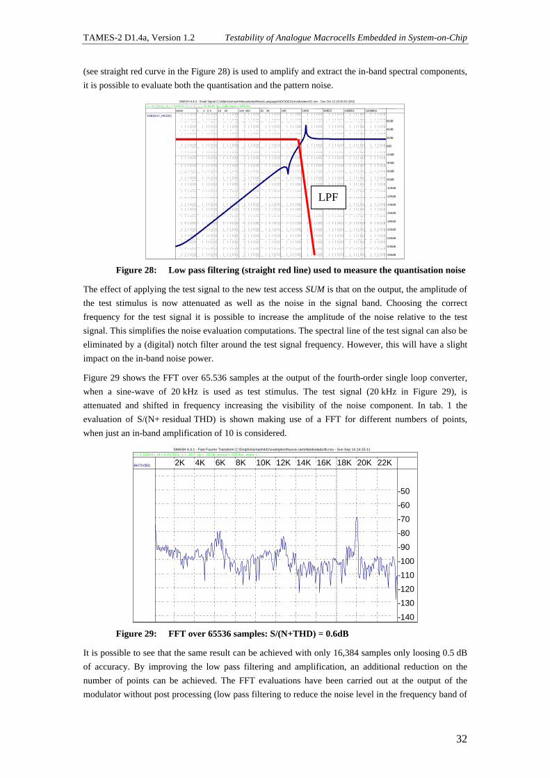
TAMES-2 D1.4a, Version 1.2 Testability of Analogue Macrocells Embedded in System-on-Chip
32
(see straight red curve in the Figure 28) is used to amplify and extract the in-band spectral components, it is possible to evaluate both the quantisation and the pattern noise.
SMASH 4.4.0 - Small Signal C:\dolphin\smash44\examples\Mixed-Language\ADC\IDEAL\modulateurAC.nsx - Sun Oct 13 18:36:03 2002 VDB(OUT_HICOD) f = 15.32KHz, df = 1.646KHz, rf = 1.12, y = -46.93dB, dy = 0dB, slope = 0dB/dec.
100m 1 2 3 4 10 20 100 200 1K 2K 10K 100K 1MEG 10MEG 100MEG
-260dB -240dB -220dB -200dB -180dB -160dB -140dB -120dB -100dB -80dB -60dB -40dB -20dB 0dB 20dB 40dB 60dB
LPF
Figure 28: Low pass filtering (straight red line) used to measure the quantisation noise
The effect of applying the test signal to the new test access SUM is that on the output, the amplitude of the test stimulus is now attenuated as well as the noise in the signal band. Choosing the correct frequency for the test signal it is possible to increase the amplitude of the noise relative to the test signal. This simplifies the noise evaluation computations. The spectral line of the test signal can also be eliminated by a (digital) notch filter around the test signal frequency. However, this will have a slight impact on the in-band noise power.
Figure 29 shows the FFT over 65.536 samples at the output of the fourth-order single loop converter, when a sine-wave of 20 kHz is used as test stimulus. The test signal (20 kHz in Figure 29), is attenuated and shifted in frequency increasing the visibility of the noise component. In tab. 1 the evaluation of S/(N+ residual THD) is shown making use of a FFT for different numbers of points, when just an in-band amplification of 10 is considered.
SMASH 4.4.1 - Fast Fourier Transform C:\Dolphin\smash441\examples\Nuova cartella\idealadc4b.nsx - Sun Sep 14 14:15:11 2003
BH7(V(B)) f = 2.326KHz, df = 4.437KHz, y = -48.7, dy = -30.98, period = 225.4us, slope = -0.00698
2K 4K 6K 8K 10K 12K 14K 16K 18K 20K 22K
-140
-130
-120
-110
-100
-90
-80
-70
-60
-50
Figure 29: FFT over 65536 samples: S/(N+THD) = 0.6dB
It is possible to see that the same result can be achieved with only 16,384 samples only loosing 0.5 dB of accuracy. By improving the low pass filtering and amplification, an additional reduction on the number of points can be achieved. The FFT evaluations have been carried out at the output of the modulator without post processing (low pass filtering to reduce the noise level in the frequency band of
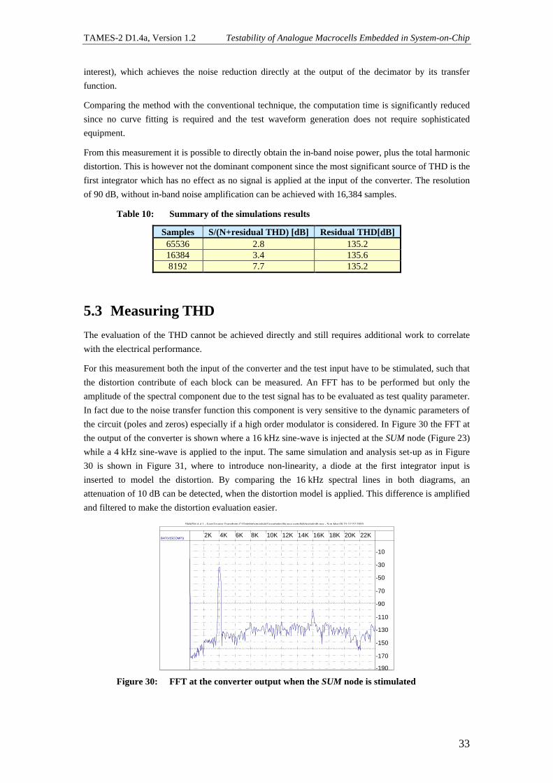
TAMES-2 D1.4a, Version 1.2 Testability of Analogue Macrocells Embedded in System-on-Chip
33
interest), which achieves the noise reduction directly at the output of the decimator by its transfer function.
Comparing the method with the conventional technique, the computation time is significantly reduced since no curve fitting is required and the test waveform generation does not require sophisticated equipment.
From this measurement it is possible to directly obtain the in-band noise power, plus the total harmonic distortion. This is however not the dominant component since the most significant source of THD is the first integrator which has no effect as no signal is applied at the input of the converter. The resolution of 90 dB, without in-band noise amplification can be achieved with 16,384 samples.
Table 10: Summary of the simulations results
Samples S/(N+residual THD) [dB] Residual THD[dB] 65536 2.8 135.2 16384 3.4 135.6 8192 7.7 135.2
5.3 Measuring THD The evaluation of the THD cannot be achieved directly and still requires additional work to correlate with the electrical performance.
For this measurement both the input of the converter and the test input have to be stimulated, such that the distortion contribute of each block can be measured. An FFT has to be performed but only the amplitude of the spectral component due to the test signal has to be evaluated as test quality parameter. In fact due to the noise transfer function this component is very sensitive to the dynamic parameters of the circuit (poles and zeros) especially if a high order modulator is considered. In Figure 30 the FFT at the output of the converter is shown where a 16 kHz sine-wave is injected at the SUM node (Figure 23) while a 4 kHz sine-wave is applied to the input. The same simulation and analysis set-up as in Figure 30 is shown in Figure 31, where to introduce non-linearity, a diode at the first integrator input is inserted to model the distortion. By comparing the 16 kHz spectral lines in both diagrams, an attenuation of 10 dB can be detected, when the distortion model is applied. This difference is amplified and filtered to make the distortion evaluation easier.
SMASH 4.4.1 - Fast Fourier Transform C:\Dolphin\smash441\examples\Nuova cartella\idealadc4b.nsx - Sun Mar 09 21:17:22 2003 BH7(V(SCOMP)) 2K 4K 6K 8K 10K 12K 14K 16K 18K 20K 22K
-190
-170
-150
-130 -110
-90
-70
-50
-30
-10
Figure 30: FFT at the converter output when the SUM node is stimulated

TAMES-2 D1.4a, Version 1.2 Testability of Analogue Macrocells Embedded in System-on-Chip
34
SMASH 4.4.1 - Fast Fourier Transform C:\Dolphin\smash441\examples\Nuova cartella\idealadc4b.nsx - Sun Mar 09 20:33:22 2003 BH7(V(SCOMP)) 2K 4K 6K 8K 10K 12K 14K 16K 18K 20K 22K
-190
-170
-150
-130 -110
-90
-70
-50
-30
-10
Figure 31: FFT at the converter output when the SUM node is stimulated and the distortion is assumed

TAMES-2 D1.4a, Version 1.2 Testability of Analogue Macrocells Embedded in System-on-Chip
35
6 Summary This deliverable documents the analysis of specification testing effectiveness of the test solutions currently under investigation for dynamic performance parameter testing. As for any novel test technique, an in-depth study needs to be performed to validate its coverage against performance parameter failure. The test solutions considered here comprise the polynomial fitting algorithm, the use of Walsh analysis, the distortion meter test methodology, and testing the noise transfer function.
Most of this work is still in progress, however, the following summary can be given:
Polynomial fitting algorithm test methodology: Future work on this test solution will need to include an assessment of test accuracy. As mentioned in section 2.3, an analysis is required to determine the coverage against failure and accuracy of test results when the test approach’s underlying assumption is violated.
Walsh Analysis test methodology: As discussed in more detail in section 3.10, page 25, this work is still in progress. The work documented here concentrates on the Walsh transform theory, assessment of stimulus accuracy requirements, preliminary simulation results for SNR testing, and initial concepts for the use on-chip tester functions. The main potential for the use of Walsh transform (applied to modulator bit-stream in response to square wave input) is seen for SNR testing. The use of this test solution promises its largest benefits in terms of test time.
Distortion meter test methodology: Simulation results for the test solution using the C-model of the modulator match FFT-based results for SNR and THD testing. If THD is lower than the noise floor, the distortion meter test method cannot compute the THD. The silicon area needed for the two notches is 8 kgates and a high accuracy test stimulus is required.
Noise transfer function tests: This test solution is currently considered for gain and SNR testing with further work addressing the potential for THD testing. Future work on this test solution, as for most discussed above as well, should address the simulation of failure modes exhibited by modulator internal (block level) faults [TAM04].
A comparison of the techniques documented here can be found in deliverable D2.2 [TAM04-1] using the decision matrix for comparison of test solutions against each other and the reference test plan.
This document is meant to replace the preliminary version (D1.4a Version 1.0) submitted in April 2003. This initial report on specification testing effectiveness forms the basis for the final report on specification testing effectiveness (deliverable D1.4b).

TAMES-2 D1.4a, Version 1.2 Testability of Analogue Macrocells Embedded in System-on-Chip
36
7 References AGI01 Agilent Technologies: Agilent 33120A function/arbitrary waveform generator data
sheet, 2001; http://cp.literature.agilent.com/litweb/pdf/5968-0125EN.pdf
ALA01 A. Alaqeeli & J. Starzyk: Hardware Implementation for Fast Convolution with a PN Code Using Field Programmable Gate Array, 33rd Southeastern Symposium on System Theory, SSST01, 19-21st March 2001, Athens, Greece, pp. 197 –201
BEA75 K. G. Beauchamp: Walsh functions and their applications, Academic Press, 1975
BEA87 K. G. Beauchamp: Transforms for Engineers, Clarendon Press Oxford, 1987
IEE01 IEEE Standard 1241-2000: IEEE standard for terminology and test methods for analog-to-digital converters, 2001
IEE04 Proposed revised Standard P1057: IEEE standard for digitizing waveform recorders, IEEE TC-10 Home Page: http://grouper.ieee.org/groups/1057/index.html
IEE94 IEEE Standard 1057-1994: IEEE standard for digitizing waveform recorders, 1994, currently withdrawn, see [IEE04]
PLA03 R. van de Plassche: CMOS integrated analog-to-digital and digital-to-analog converters, 2nd edition, Kluwer Academic Publishers, 2003
ROY02 A. Roy, S. Sunter, A. Fudoli & D. Appello: High accuracy stimulus generation for A/D converter BIST, IEEE International Test Conference, ITC02, 8-10th Oct. 2002, Baltimore, MD, USA, pp. 1031-1039
STO91 D. S. Stoffer: Walsh-Fourier analysis and its statistical applications, Journal of the American Statistical Association, 2001, vol. 86, no. 414, pp. 461-479
SUN97 S. K. Sunter & N. Nagi: A simplified polynomial-fitting algorithm for DAC and ADC BIST, IEEE International Test Conference, ITC97, 3-5th Nov. 1997, Washington, DC, USA, pp. 389-395
TAM02 K. Georgopoulos, M. Burbidge, A. Lechner, A. Richardson & D. De Venuto: Review of test strategies and resources used in high-resolution interface testing, Deliverable 1.1 version 1.2, TAMES-2, IST Project 2001-34283, 2002
TAM02-1 IMSE: Initial results based of modeling the correlation between circuit level performance and design specifications, Deliverable 1.3, TAMES-2, IST Project 2001-34283, 2002
TAM03 O. Guerra, D. De Venuto, E. Compagne & R. Vanhooren: Initial summary of Dft possibilities for high-resolution interfaces, Deliverable 2.1a version 1.0, TAMES-2, IST Project 2001-34283, 2003
TAM04 K. Georgopoulos, M. Burbidge, A. Lechner, A. Richardson & D. De Venuto: Compilation of potential circuit failure modes for high-resolution interfaces, Deliverable 1.2 version 1.1, TAMES-2, IST Project 2001-34283, 2004
TAM04-1 Dolphin Integration: Selection of DfT techniques for high-resolution interfaces, Deliverable 2.2 version 1.0, TAMES-2, IST Project 2001-34283, 2004
VEN04 D. De Venuto New Test Access for High Resolution SD ADC’s by using the Noise Transfer Function Evaluation; Proc. Of International Symposium on Quality in Electronic Design, ISQED04, 22-24 March2004, San Jose, CA. USA.