1 FINUDA Status Report 30th Scientific Committee Meeting LNF, 23.05.05 A. Filippi – INFN Torino.

INFN sez. di Torino
CMOS process example
Gianni Mazza

Main steps
Gianni Mazza
� FEOL ( Front End Of the Line )� up to the transistor creation
� BEOL ( Back End Of the Line )� metalization
The two steps correspond to different design teams and are treated separately

Problem� Substrate is either p doped or n doped� PMOS requires n doped substrate� NMOS requires p doped substrate
� Is it possible to have both PMOS and NMOS on the same substrate ?
Gianni Mazza

Solution : well ( or tub )A n-doped ( p-doped ) region is implanted on a p-doped ( n-doped ) substrate.CMOS process : Complementary MOS process
Gianni Mazza

Considerations
� Well and substrate creates a p-n junction� Reduced mobility in the well� P-well vs. n-well� Source-bulk connection� Twin well and pseudo twin well processes� Triple well
Gianni Mazza
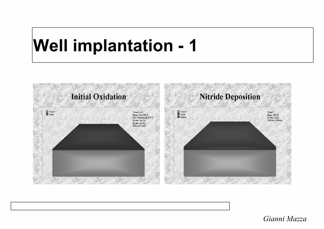
Well implantation - 1
Gianni Mazza
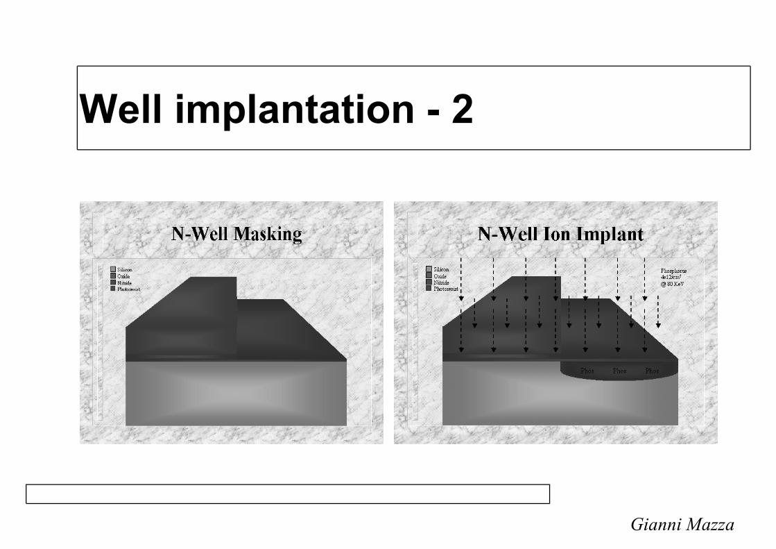
Well implantation - 2
Gianni Mazza
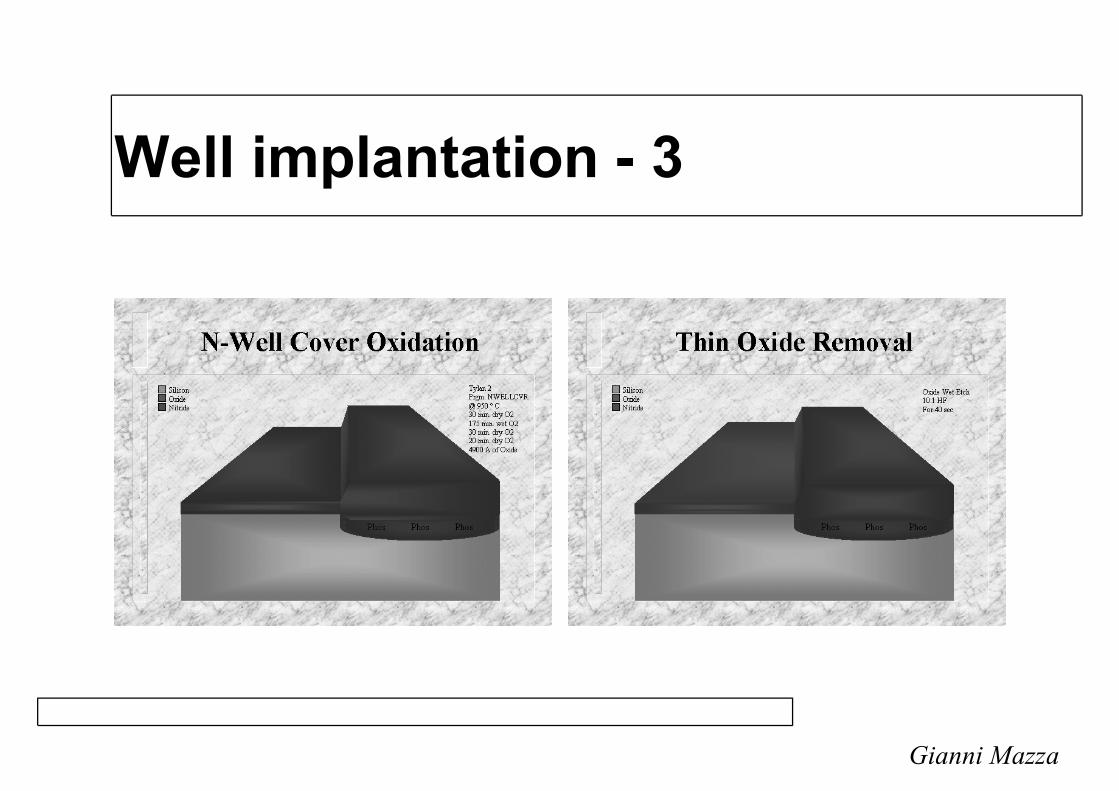
Well implantation - 3
Gianni Mazza

Well implantation - 4
Gianni Mazza
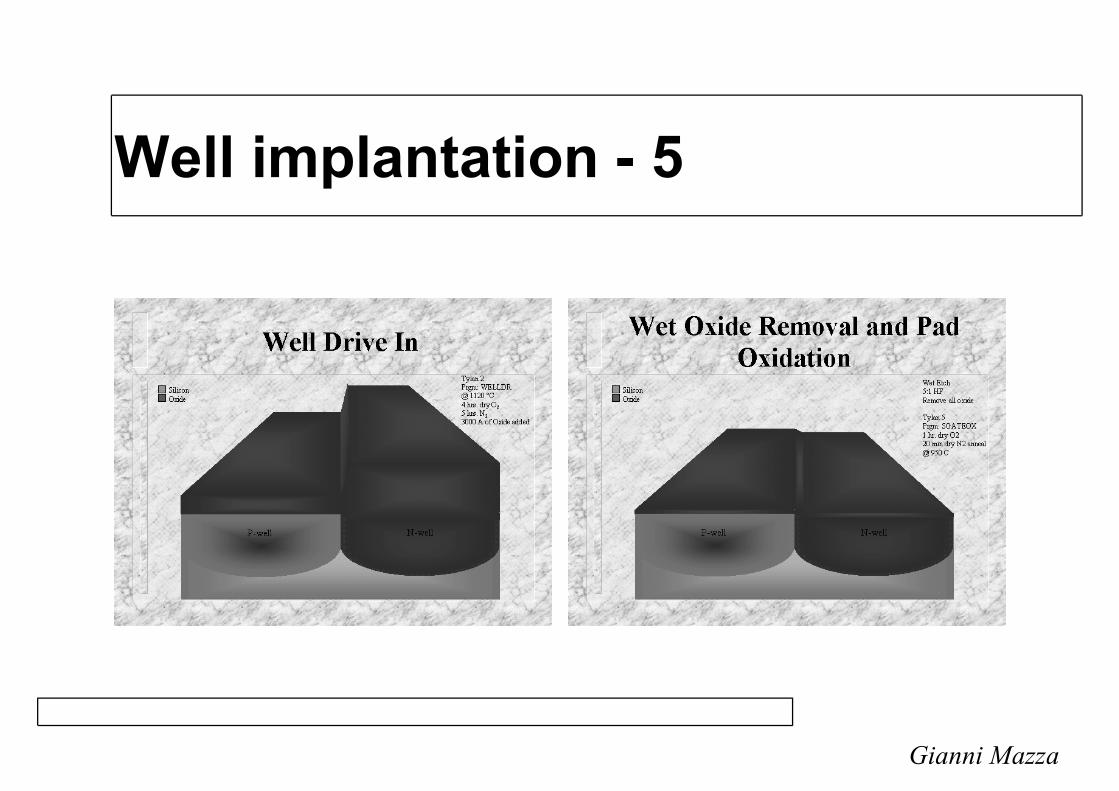
Well implantation - 5
Gianni Mazza

Field implant - 1
Gianni Mazza
Field implant - 2
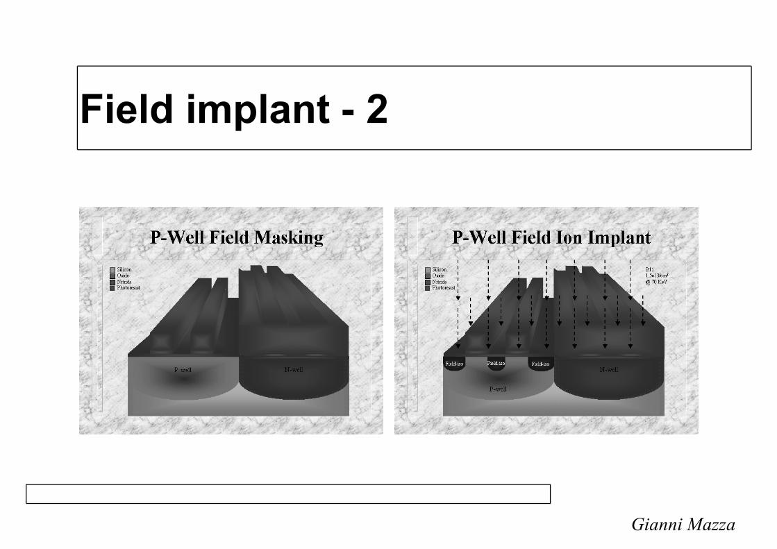
Gianni Mazza
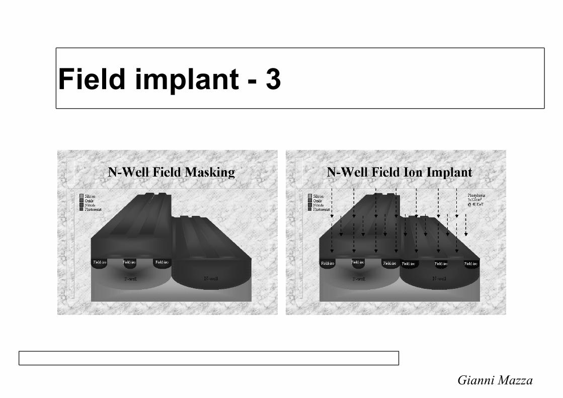
Field implant - 3
Gianni Mazza

LOCOS - 1
Gianni Mazza
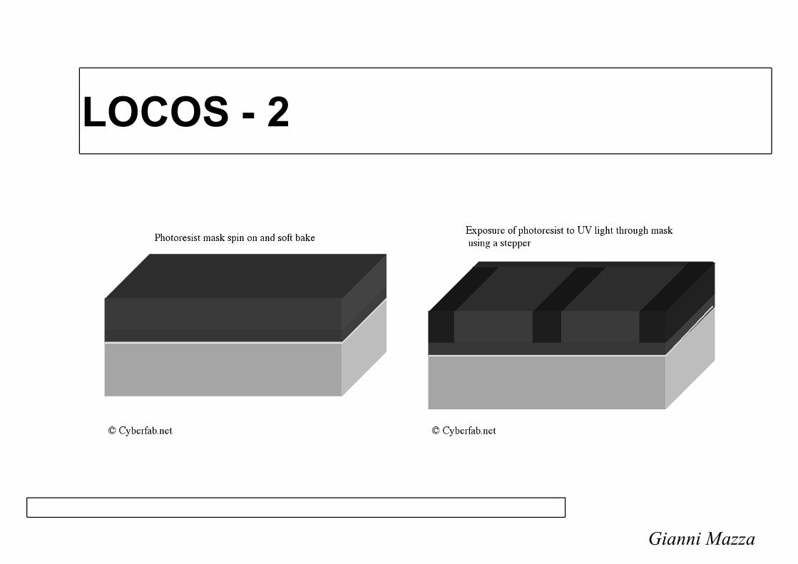
LOCOS - 2
Gianni Mazza

LOCOS - 3
Gianni Mazza

LOCOS - 4
Gianni Mazza

LOCOS - 5
Gianni Mazza

Parasitic MOS - 1
Gianni Mazza

Parasitic MOS - 2
Gianni Mazza

Bird�s beak
Gianni Mazza
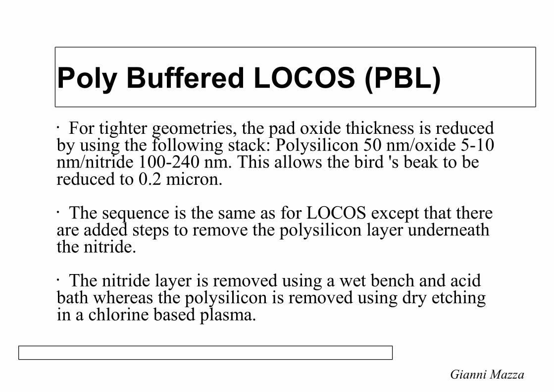
Poly Buffered LOCOS (PBL)� For tighter geometries, the pad oxide thickness is reduced by using the following stack: Polysilicon 50 nm/oxide 5-10 nm/nitride 100-240 nm. This allows the bird 's beak to be reduced to 0.2 micron. � The sequence is the same as for LOCOS except that there are added steps to remove the polysilicon layer underneath the nitride.� The nitride layer is removed using a wet bench and acid bath whereas the polysilicon is removed using dry etching in a chlorine based plasma.
Gianni Mazza

Deep trench isolation - 1
Gianni Mazza
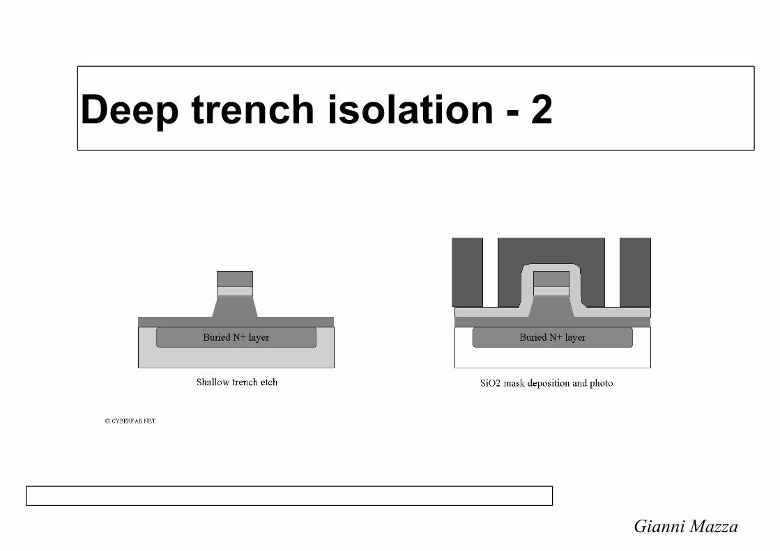
Deep trench isolation - 2
Gianni Mazza
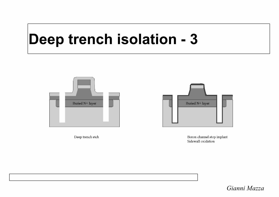
Deep trench isolation - 3
Gianni Mazza

Deep trench isolation - 4
Gianni Mazza

Deep trench isolation - 5
Gianni Mazza

Deep trench isolation - 6
Gianni Mazza
Plasma-Enhanced TetraEthylOrthoSilicate
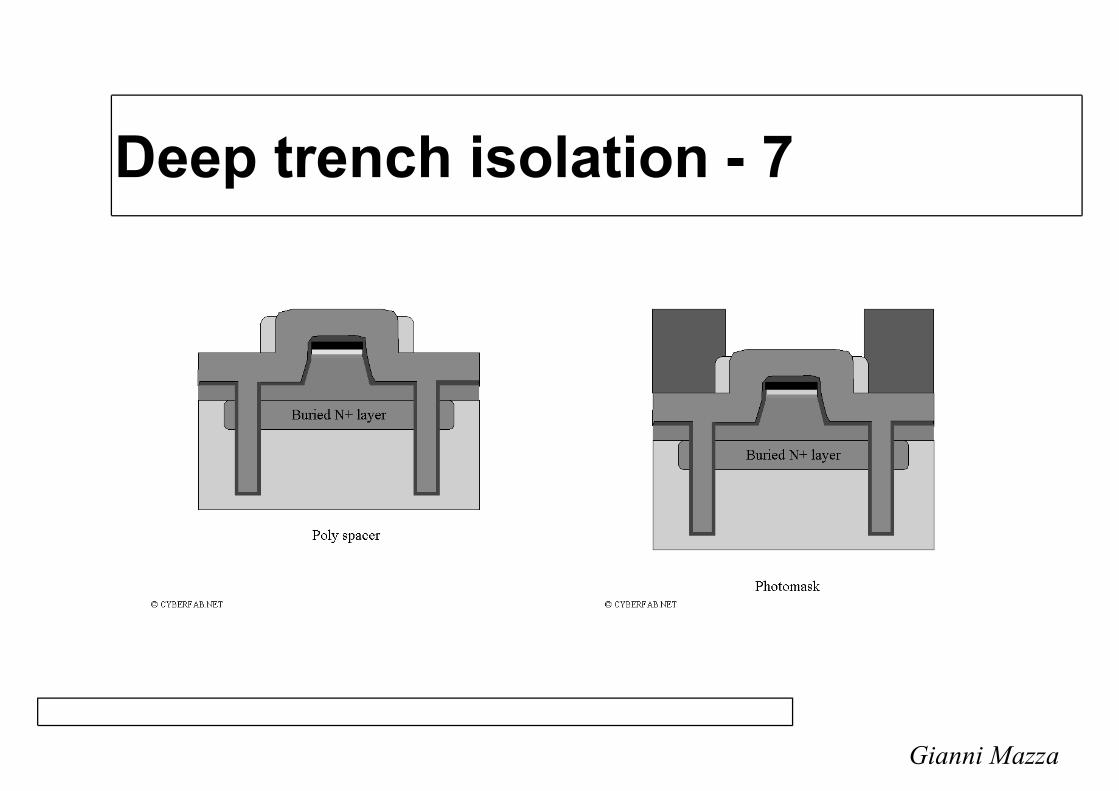
Deep trench isolation - 7
Gianni Mazza

Deep trench isolation - 8
Gianni Mazza

Deep trench isolation - 9
Gianni Mazza

Isolation Technologies
Gianni Mazza
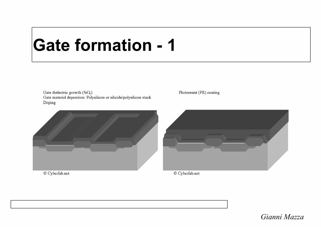
Gate formation - 1
Gianni Mazza
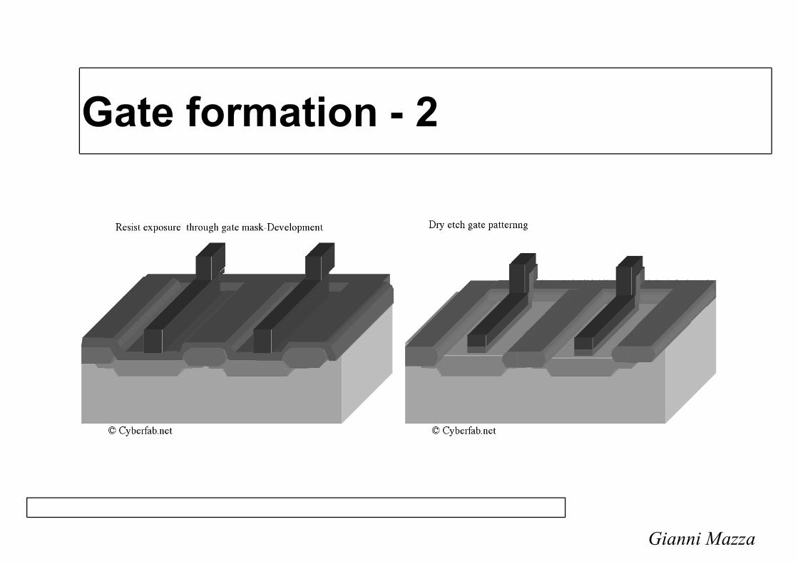
Gate formation - 2
Gianni Mazza
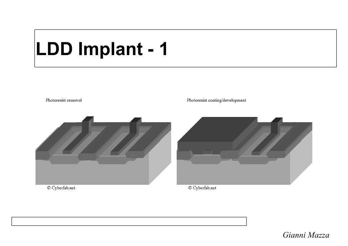
LDD Implant - 1
Gianni Mazza

LDD Implant - 2
Gianni Mazza

LDD Implant - 3
Gianni Mazza

Spacer
Gianni Mazza

NMOS S/D implant
Gianni Mazza

PMOS S/D implant

Silicide formation
Gianni Mazza
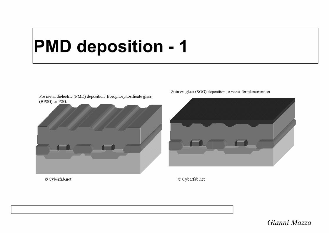
PMD deposition - 1
Gianni Mazza

PMD deposition - 2
Gianni Mazza
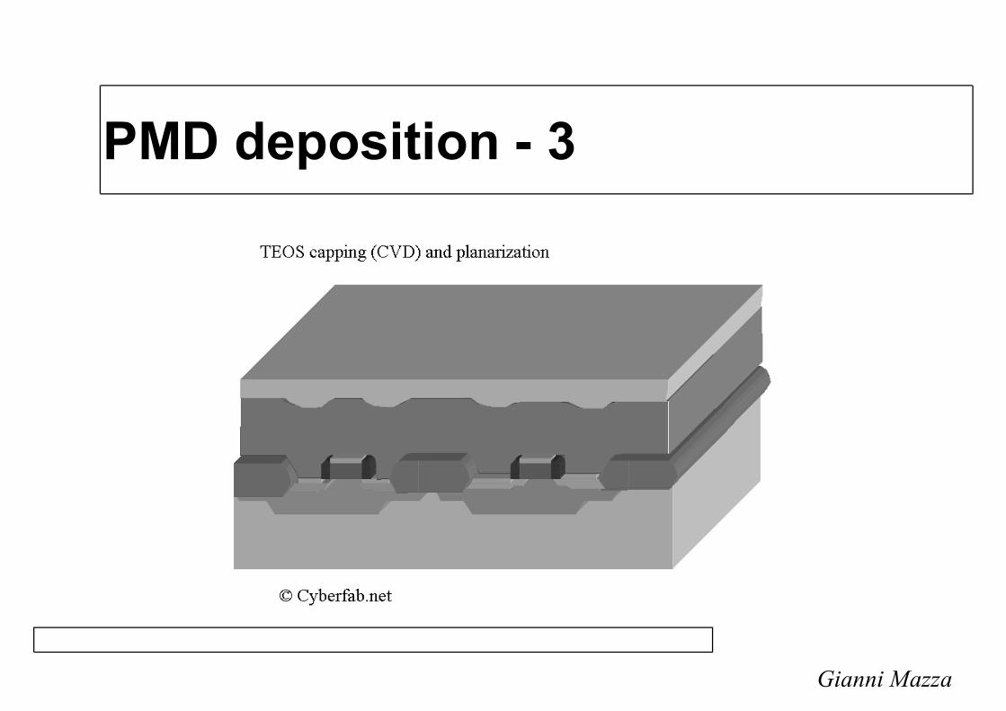
PMD deposition - 3
Gianni Mazza

Contact formation - 1
Gianni Mazza

Contact formation - 2
Gianni Mazza

W fill - 1
Gianni Mazza
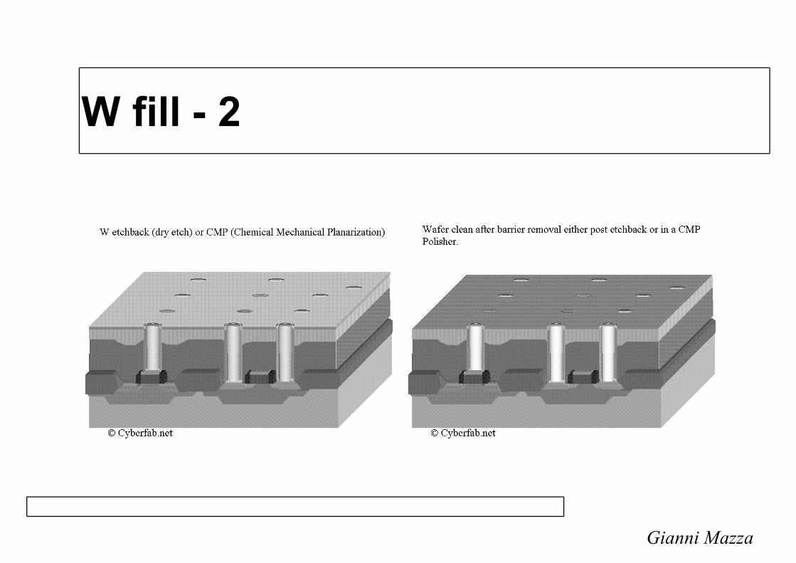
W fill - 2
Gianni Mazza

First metal layer - 1
Gianni Mazza

First metal layer - 2
Gianni Mazza
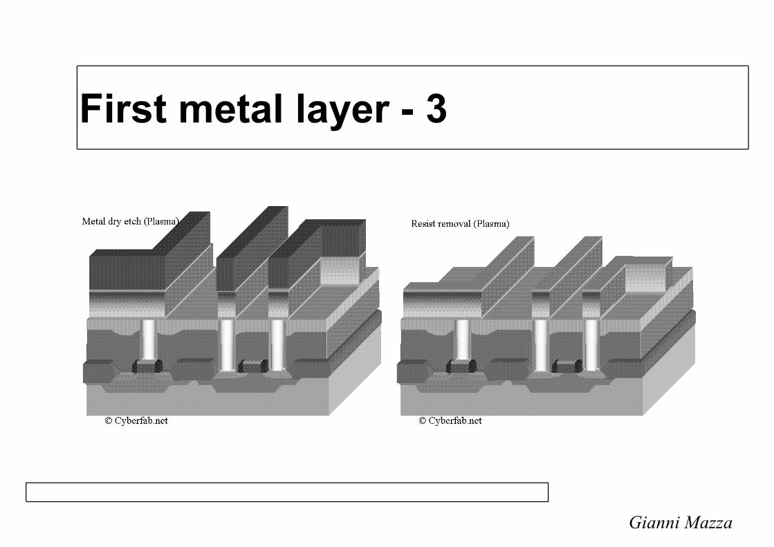
First metal layer - 3
Gianni Mazza

Inter-metal dielectric - 1
Gianni Mazza

Inter-metal dielectric - 2
Gianni Mazza

Via etch
Gianni Mazza

W fill - 1
Gianni Mazza

W fill - 2
Gianni Mazza

Second metal layer
Gianni Mazza

Final cross section
Gianni Mazza
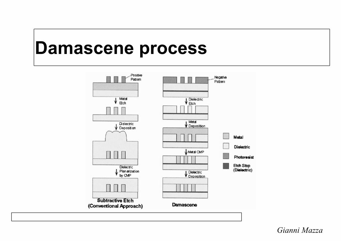
Damascene process
Gianni Mazza

BiCMOS technology
Gianni Mazza
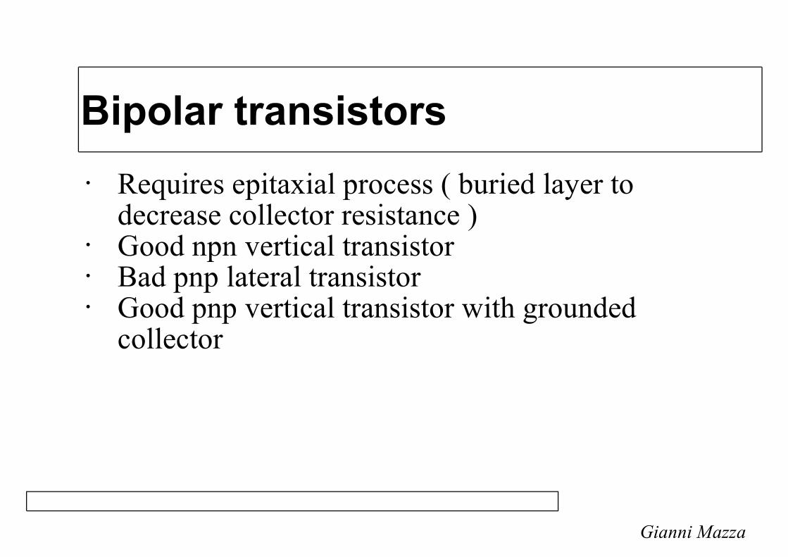
Bipolar transistors� Requires epitaxial process ( buried layer to
decrease collector resistance )� Good npn vertical transistor� Bad pnp lateral transistor� Good pnp vertical transistor with grounded
collector
Gianni Mazza
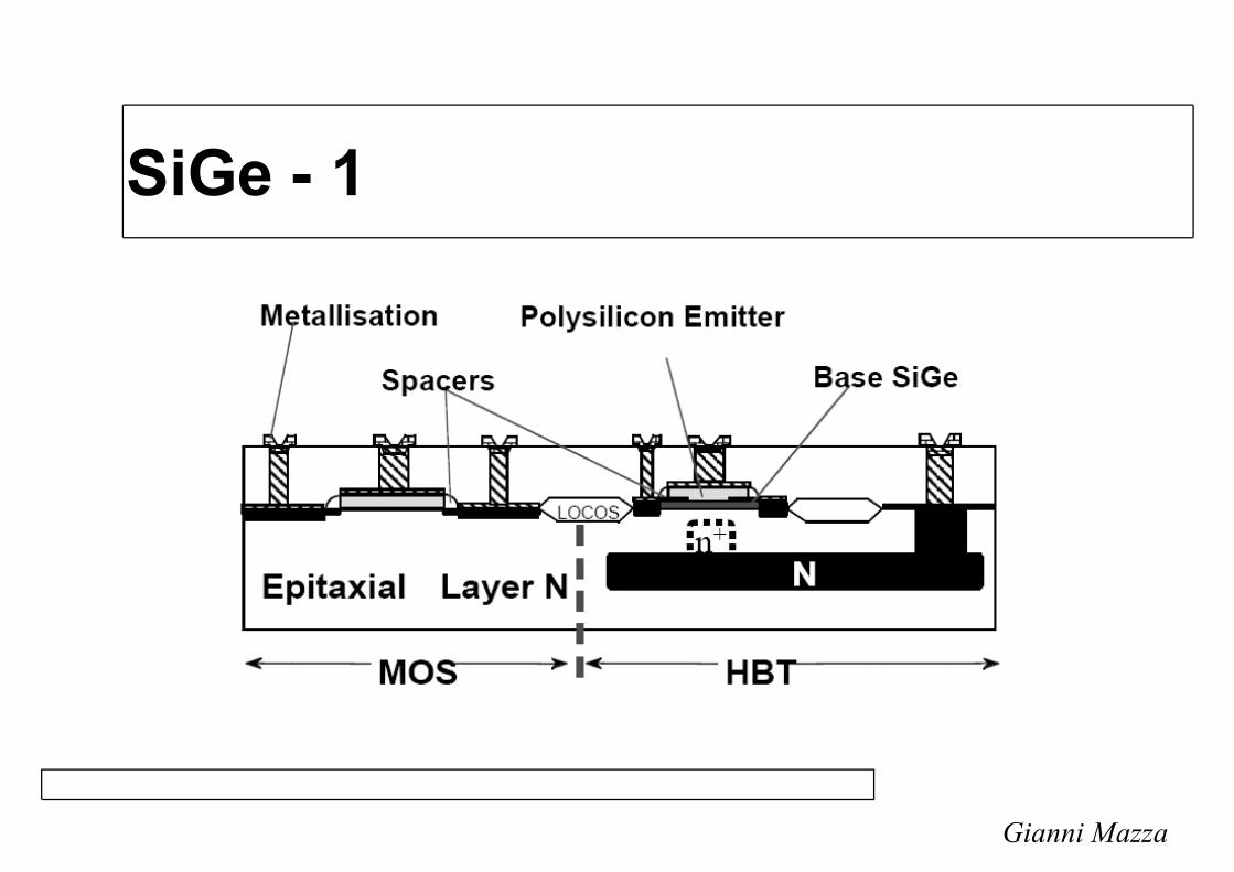
SiGe - 1
Gianni Mazza

SiGe - 2
Gianni Mazza

Latch-up - 1
Gianni Mazza

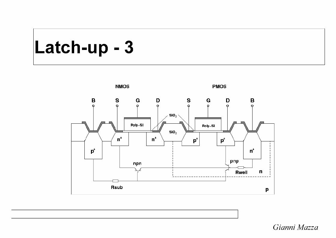

Latch-up - 4
Gianni Mazza
To prevent latch-up :
� Substrate contacts to lower RS and R
W� Increase distance between nMOS and nWell� Shallow Trench Insulation� SOI technologies

SOI process
Gianni Mazza

SOI techniques
Gianni Mazza
� Wafer bonding and etch back� Silicon on sapphire/zirconia (Zr
2O)
� Recrystallization from the melt� Selective epitaxy over holes in the oxide (ELO)� Porous silicon (FIPOX)� Oxygen implantation (SIMOX)� Silicon-On-Nothing (SON)

SOI structure
Gianni Mazza

Parasitic capacitance
Gianni Mazza

Tolerance to SEU
Gianni Mazza

3-D ICs
Gianni Mazza

µChannel cooling
Gianni Mazza