Influence of RTA Parameters on Residual Stress and Stress ...
7
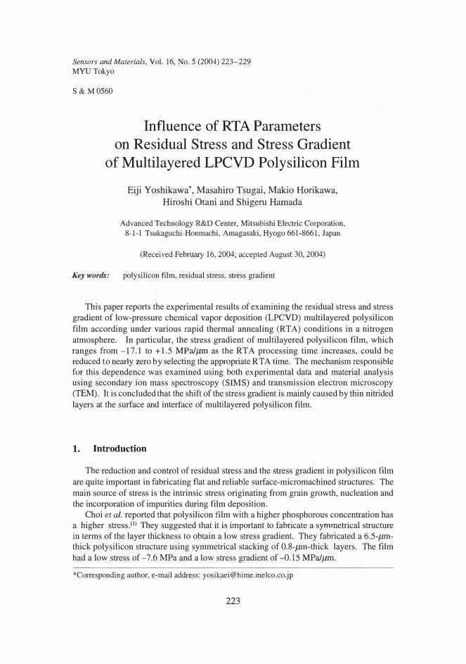
Sensors and Materials, Vol. 16, No. 5 (2004) 223-229 MYUTokyo S &M 0560 Influence of RTA Parameters on Residual Stress and Stress Gradient of Multilayered LPCVD Polysilicon Film Eiji Yoshikawa*, Masahiro Tsugai, Makio Horikawa, Hiroshi Otani and Shigeru Hamada Advanced Technology R&D Center, Mitsubishi Elecic Corporation, 8-1-1 Tsukaguchi-Honmachi, Amagasi, Hyogo 661-8661, Japan (Received Febru 16, 2004; accepted August 30, 2004) Key words: polysilicon film, residual stress, sess gradient This paper reports the experimental results of examining the residual stress and stress gradient of low-pressure chemical vapor deposition (LPCVD) multilayered polysilicon film according under various rapid thermal annealing (RTA) conditions in a nitrogen atmosphere. In particular, the stress gradient of multilayered polysilicon film, which ranges om -17.1 to +1.5 MPµm as the RTA processing time increases, could be reduced to nearly zero by selecting the appropriate RTA me. The mechism responsible for this dependence was examined using both experimental data and material analysis using secondary ion mass spectroscopy (SIMS) and transmission electron microscopy (TEM). It is concluded that the shift of the stress gradient is mainly caused by thin nitrided layers at the surface and interface of multilayered polysilicon film. 1. Introduction The reduction and control of residual stress and the sess gradient in polysilicon film are quite important in bricating flat and reliable surface-micromachined structures. The main source of stress is the intrinsic stress originating om grain growth, nucleation and the incorporation of impurities during film deposition. Choi et al. reported that polysilicon film with a higher phosphorous concenation has a higher stress. OJ They suggested that it is important to fabricate a syetrical sucture fo terms of the layer thickness to obtain a low stress gradient. They fabricated a 6.5-µm- thick polysilicon structure using symmetrical stacking of 0.8-µm-thick layers. The film had a low stress of-7.6 MPa and a low stress gradient of-0.15 MPµm. *Corresponding author, e-mail adess: yosikaei@hime.melco,co.jp 223
Transcript of Influence of RTA Parameters on Residual Stress and Stress ...
Sensors and Materials, Vol. 16, No. 5 (2004) 223-229 MYUTokyo
S &M 0560
Influence of RTA Parameters
on Residual Stress and Stress Gradient
of Multilayered LPCVD Polysilicon Film
Eiji Yoshikawa*, Masahiro Tsugai, Makio Horikawa, Hiroshi Otani and Shigeru Hamada
Advanced Technology R&D Center, Mitsubishi Electric Corporation, 8-1-1 Tsukaguchi-Honmachi, Amagasaki, Hyogo 661-8661, Japan
(Received February 16, 2004; accepted August 30, 2004)
Key words: polysilicon film, residual stress, stress gradient
This paper reports the experimental results of examining the residual stress and stress gradient of low-pressure chemical vapor deposition (LPCVD) multilayered polysilicon film according under various rapid thermal annealing (RTA) conditions in a nitrogen atmosphere. In particular, the stress gradient of multilayered polysilicon film, which ranges from -17.1 to +1.5 MPa/µm as the RTA processing time increases, could be reduced to nearly zero by selecting the appropriate RT A time. The mechanism responsible for this dependence was examined using both experimental data and material analysis using secondary ion mass spectroscopy (SIMS) and transmission electron microscopy (TEM). It is concluded that the shift of the stress gradient is mainly caused by thin nitrided layers at the surface and interface of multilayered polysilicon film.
1. Introduction
The reduction and control of residual stress and the stress gradient in polysilicon film are quite important in fabricating flat and reliable surface-micromachined structures. The main source of stress is the intrinsic stress originating from grain growth, nucleation and the incorporation of impurities during film deposition.
Choi et al. reported that polysilicon film with a higher phosphorous concentration has a higher stress. OJ They suggested that it is important to fabricate a symmetrical structure fo terms of the layer thickness to obtain a low stress gradient. They fabricated a 6.5-µmthick polysilicon structure using symmetrical stacking of 0.8-µm-thick layers. The film had a low stress of-7.6 MPa and a low stress gradient of-0.15 MPa/µm.
*Corresponding author, e-mail address: [email protected],co.jp
223
224 Sensors and Materials, Vol. 16, No. 5 (2004)
It is widely known that oxidation of polysilicon film induces a compressive stress. Lee et al. found that the thin oxidized layer formed at the interface of multistacked polysilicon films plays an important role in governing the stress gradient.<2J This interface effect could
be minimized by the symmetrical stacking of polysilicon films, which resulted in a low
stress gradient of-0.15 MPa/µm for a 5.3-µm-thick polysilicon layer. Ftirtsch et al. confirmed that the diffusion of oxygen atoms causes stress changes. <3l The
stress and stress gradient can be changed by subsequent annealing in an oxygen and nitrogen ambient.
All the above researchers used a conventional annealing furnace to reduce the stress and the stress gradient. We used RT A for this purpose and succeeded in reducing the stress
and the stress gradient. To study the mechanism for reducing the stress gradient, we carried
out several analyses.
2. Materials and Methods
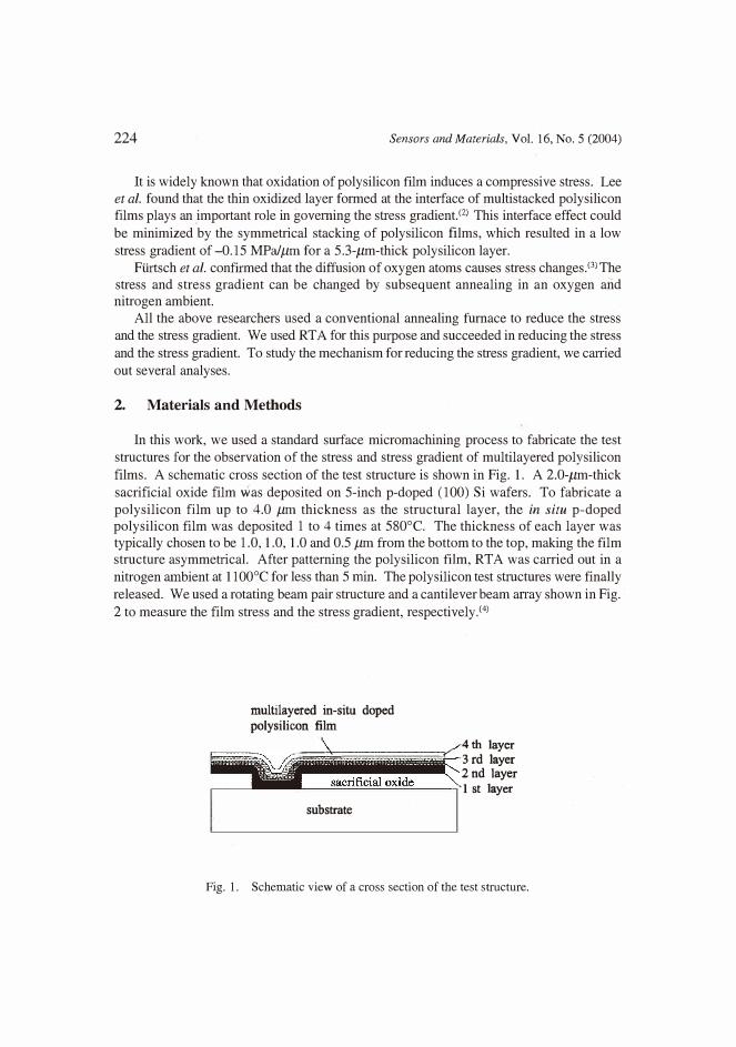
In this work, we used a standard surface micromachining process to fabricate the test structures for the observation of the stress and stress gradient of multilayered polysilicon
films. A schematic cross section of the test structure is shown in Fig. 1. A 2.0-µm-thick
sacrificial oxide film was deposited on 5-inch p-doped (100) Si wafers. To fabricate a polysilicon film up to 4.0 µm thickness as the structural layer, the in situ p-doped polysilicon film was deposited 1 to 4 times at 580°C. The thickness of each layer was typically chosen to be 1.0, 1.0, 1.0 and 0.5 µm from the bottom to the top, making the film structure asymmetrical. After patterning the polysilicon film, RTA was carried out in a
nitrogen ambient at 1100°C for less than 5 min. The polysilicon test structures were finally
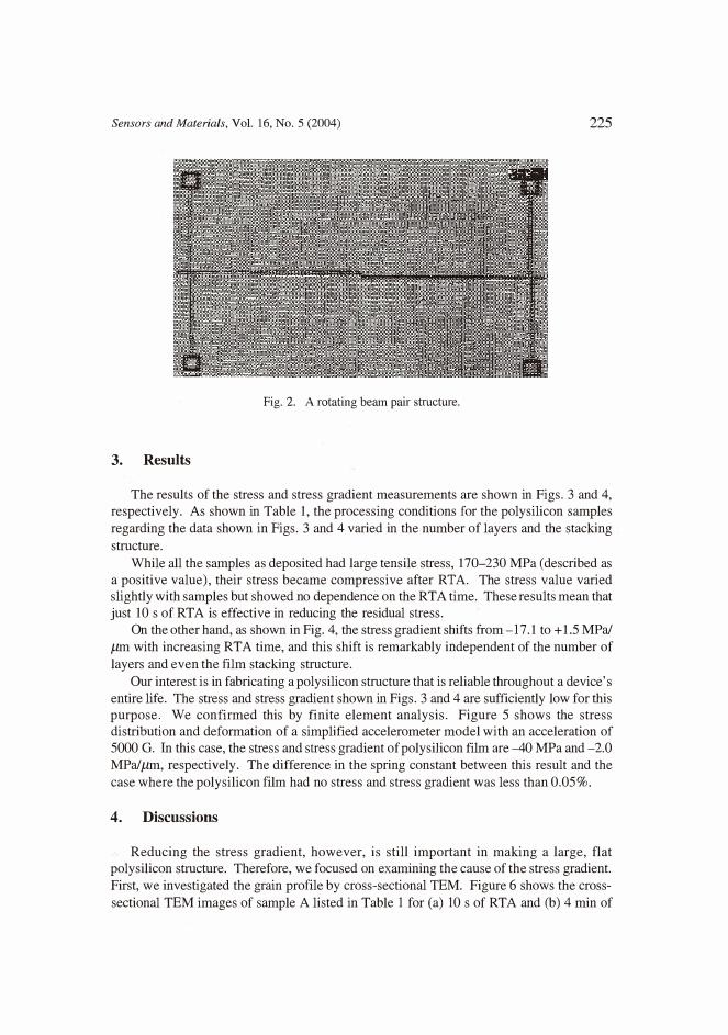
released. We used a rotating beam pair structure and a cantilever beam array shown in Fig.
2 to measure the film stress and the stress gradient, respectively.<4J
multilayered in-situ doped polysilicon film
4th layer --=
=
='=======::r' 3 rd layer 2nd layer
----------� ·1 st layer substrate
Fig. 1. Schematic view of a cross section of the test structure.
Sensors and Materials, Vol. 16, No. 5 (2004) 225
Fig. 2. A rotating beam pair structure.
3. Results
The results of the stress and stress gradient measurements are shown in Figs. 3 and 4,
respectively. As shown in Table 1, the processing conditions for the polysilicon samples
regarding the data shown in Figs. 3 and 4 varied in the number of layers and the stacking
structure.
While all the samples as deposited had large tensile stress, 170-230 MPa ( described as
a positive value), their stress became compressive after RTA. The stress value varied
slightly with samples but showed no dependence on the RTA time. These results mean that
just 10 s of RTA is effective in reducing the residual stress.
On the other hand, as shown in Fig. 4, the stress gradient shifts from -17 .1 to + 1.5 MPa/
µm with increasing RT A time, and this shift is remarkably independent of the number of
layers and even the film stacking structure.
Our interest is in fabricating a polysilicon structure that is reliable throughout a device's
entire life. The stress and stress gradient shown in Figs. 3 and 4 are sufficiently low for this
purpose. We confirmed this by finite element analysis. Figure 5 shows the stress
distribution and deformation of a simplified accelerometer model with an acceleration of
5000 G. In this case, the stress and stress gradient of polysilicon film are -40 MPa and -2.0
MPa/µm, respectively. The difference in the spring constant between this result and the
case where the polysilicon film had no stress and stress gradient was less than 0.05%.
4. Discussions
Reducing the stress gradient, however, is still important in making a large, flat
polysilicon structure. Therefore, we focused on examining the cause of the stress gradient.
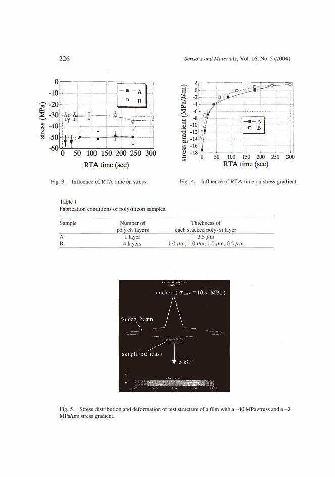
First, we investigated the grain profile by cross-sectional TEM. Figure 6 shows the cross
sectional TEM images of sample A listed in Table 1 for (a) 10 s of RTA and (b) 4 min of
226
0 rr---,----,-r--;:=:==�
-10 1-+-------,---+----+-------l - • - A-o-B
"2'-20r·1--,-----r----r-----i..--�
6-30r·to±c�=-i;,-1----t--�•···�···�···�+�····�···��ICll Cll -40 r·t-----,---+-----t---,-----t----, I
-50
-60O 50 100 150 200 250 300
RTA time (sec)
Fig. 3. Influence of RTA time on stress.
Table 1 Fabrication conditions of polysilicon samples.
Sample
A B
Number of poly-Si layers
I layer 4 layers
_ Sensors and Materials, Vol. 16, No. 5 (2004)
2 i---,---------=-r=:�====oi8 o�-··· · ·····••S••·•·· ········ \ij·•·<�»i='.'.=······ ·········> ···········jl
� -2 H···················+i:1,�,._111--F--'--
-4 �,. . .. ti,,;( .... .......... ··-.. ........... . . .......... ; ... ················· ....... ,,.,
� -6ric.J··· ····I···· ···· •····· '::" -S�''Il'f--+-- -1 r---,
� -lOr-:,1-� --· 1 :a -121-1!'1'········· ·····•·········· ····· ·····•· · ··· ,_ __ ,-1--�- -.1(,:I 5h -141-1·'/······ · ······'·············· ····'··Cll -16r·'I···· ············· ·•····· ···· Cll i2 -18�-�-�-�-�-�-�... 0 50 100 150 200 250 300 Cll
RTA time (sec)
Fig. 4. Influence of RTA time on stress gradient.
Thickness of each stacked poly-Si layer
3.5µm
1.0 µm, 1.0 µm, 1.0 µm, 0.5 µm
Fig. 5. Stress distribution and deformation of test suucture of a film with a -40 MPa stress and a -2 MPa/µm stress gradient.
Sensors and Materials, Vol. 16, No. 5 (2004) 227
(a) (b)
Fig. 6. Cross-sectional TEM images of poly-Si sample A listed in Table 1: (a) 10 s RTA and (b) 4
minRTA.
RTA. From these TEM images, we obtained the grain size distributions. Although grain growth is observed as RTA time increases, a distribution in the thickness direction correlating to the stress gradient is not observed. From the results in Figs. 3, 4 and 6, it is concluded that grain-growth due to the increasing RTA time up to 5 min has no correlation
with the stress gradient.
Therefore, we assumed that the stress gradient is correlated in some way with the
profile of the impmities contained in the polysilicon film. To explain the stress gradient
behavior, we developed a model consistent with the results in which the stress gradient shifts from negative to positive with increasing RTA time. We focused on the well-known phenomena that oxidized silicon film induces a compressive stress and that nitrided silicon
film has a tensile stress. The model shown in Fig. 7 illustrates the schematic stress
distribution in the thickness direction of a multilayered polysilicon film. We assumed that
the total stress gradient of the multilayered polysilicon film is governed mainly by the
stress of the polysilicon layer, the oxidized layer and the nitrided layer. The total bending moment is equal to the residual stress multiplied by the distance between that layer and the midpoint of the film thickness. If this assumption is correct, the total stress gradient shows a correlation with the concentration of oxygen and nitrogen atoms in a polysilicon film and the location of these atoms.
To confirm the appropriateness of this model, we carried out an SIMS on sample B
listed in Table 1. The concentration profiles in the thickness direction are shown in Fig. 8,
for (a) as-deposited and (b) annealed in the RTA furnace for 4 min. A large amount of
oxygen accumulated at each interface of the film. Although other atoms also seem to have peaks at the same interfaces, these are mainly caused by a peculiarity of the analyzer in that the sensitivity is increased in the oxygen-rich region. Phosphorous is uniformly distributed throughout the film in both cases. Therefore, the difference between these results is just the
nitrogen concentration at the interface. The nitrogen atoms pile up at the interface due to

,.-..,
u VJ
VJ
u
.€ VJ
Q)
228
thickness
nitride-rich region
amorphous Si
Sensors and Materials, Vol. 16, No. 5 (2004)
thickness
oxygen rich oxygen rich region
-
nitride -rich region region poly-Si
compressive 0 tensile compressive 0 tensile
103
102
101
100
103
102
101
100
105
104
(-) (+) (-) (+) (a) (b)
Fig. 7. Schematic stress distribution of test structure: (a) sample B (4 layers, as deposited); (b) sample B (4 layers, 4 min RTA).
top bottom 4th 3rd 2nd I st
: layer: layer layer layer
0
Si :
p
0 500 1000 1500 2000 2500 3000
sputtering time (sec)
(a)
,.-.., 10°
103
Q) VJ
VJ
102
101
......
10°
Q)
105
104
top 4th
i Jaye/ 3rd
layer 2nd layer
P'
bottom I st
layer I
0 500 1000 1500 2000 2500 3000
sputtering time (sec)
(b)
Fig. 8. SIMS concentration profiles of sample B listed in Table 1: (a) as deposited and (b) annealed at 1100°c by RTA for 4 min.
Sensors and Materials, Vol. 16, No. 5 (2004) 229
RTA. Considering the results shown in Figs. 3 and 5 in which no meaningful correlation
between stress gradient and grain structure was observed, it is concluded that the shift of
the stress gradient from negative to positive is mainly caused by the thin nitride-rich region
at the surface and the interface of the multilayered polysilicon film. As is the case of multi
layered film, single-layered film has a nitride-rich region at the surface.
5. Conclusions
We have presented a study of the influence of RTA on the residual stress and stress
gradient of multilayered LPCVD polysilicon film. In contrast to the fact that grain growth by extending the RTA time has no significant influence on stress, the decisive factor for the
shift of the stress gradient is the duration of the RTA. The stress gradient of multilayered
polysilicon film, which ranges from -17.1 to+ 1.5 MPa/µm as the RTA time increases, can
be reduced to nearly zero by setting the RTA time to approximately 150 s. Our method
which uses less than 3 min of RTA to fabricate large polysilicon structures can lower the
thermal budget much more than other methods which require annealing in a conventional
furnace for several hours. We confirmed that the shift of the stress gradient is mainly
caused by the thin nitride-rich region at the surface and the interface of multilayered polysilicon film.
Acknowledgement
The authors wish to thank Dr. S. Tani, Advanced Technology R&D Center, Mitsubishi
Electric Corporation, Japan, for invaluable advice. We are also grateful to Ms. M.
Okumura, Mr. K. Sato, Y. Yamaguchi and the members of Kumamoto Works, for their
enthusiastic help with the fabrication.
References
C. A. Choi, C. S. Lee, W. I. Jang, Y. S. Hong, J. H. Lee and B. K. Sohn: Jpn. J. Appl. Phys. 38
(1999) 3693.
2 C. S. Lee, J. H. Lee, C. A. Choi, K. No and D. M. Wee: Journal of Micromechanics and
Microengineering 9 (1999) 252.
3 M. Furtsch, M. Offenberg, H. Miinzel and J. R. Morante: Sens. Actuators A 76 (1999) 335.
4 B. P. van Drieenhuizen, J. F. L. Goosen, P. J. French and R. F. Wolffenbuttel: Sens. Actuators
A 37-38 (1993) 756.