influence of germanium concentration and homogeneous boron
205
1 INFLUENCE OF GERMANIUM CONCENTRATION AND HOMOGENEOUS BORON DOPING ON MICROSTRUCTURE, KINETICS, AND SHEET RESISTANCE OF NICKEL GERMANOSILICIDE THIN FILMS By JOHN SAMUEL MOORE A DISSERTATION PRESENTED TO THE GRADUATE SCHOOL OF THE UNIVERSITY OF FLORIDA IN PARTIAL FULFILLMENT OF THE REQUIREMENTS FOR THE DEGREE OF DOCTOR OF PHILOSOPHY UNIVERSITY OF FLORIDA 2008
Transcript of influence of germanium concentration and homogeneous boron
1
INFLUENCE OF GERMANIUM CONCENTRATION AND HOMOGENEOUS BORON DOPING ON MICROSTRUCTURE, KINETICS, AND SHEET RESISTANCE OF NICKEL
GERMANOSILICIDE THIN FILMS
By
JOHN SAMUEL MOORE
A DISSERTATION PRESENTED TO THE GRADUATE SCHOOL OF THE UNIVERSITY OF FLORIDA IN PARTIAL FULFILLMENT
OF THE REQUIREMENTS FOR THE DEGREE OF DOCTOR OF PHILOSOPHY
UNIVERSITY OF FLORIDA
2008

2
© 2008 John Samuel Moore

3
In memory of Dr. Richard Connell. May all who teach aspire to his example.

4
ACKNOWLEDGMENTS
Life is a long journey, and one not traveled alone. On a personal level, I thank my family
first and foremost. Without their love and support, this document would never have been
possible. I also express gratitude to the innumerable teachers who have helped me through my
23 years of education. I particularly recognize some of my high school Advanced Placement
English, science, and math teachers, Ms. Miles, Mrs. O�’Connor, Mrs. Slotnick, and Mr.
Lederberg, who gave me the tools and foundation for a successful undergraduate and graduate
education. My thanks are also extended to the late Dr. Richard Connell, for whom this work is
dedicated, for being an outstanding professor and role model throughout my undergraduate
degree. My dear friend and staunch supporter, Dr. Michelle Phen, is also acknowledged for her
unending assistance with the development and editing of this work. I love you!!!!
On a professional level, I thank Hans Weijtmans and Dr. Mark Visokay, formerly of
Texas Instruments, Inc., for growing the experimental structures used in this work. I also thank
the staff, especially Kerry Siebein and Dr. Jerry Bourne, of the Major Analytical Instrumentation
Center (MAIC) at the University of Florida for their assistance in TEM and SEM sample
analysis. I also thank Mikhail Klimov of AMPAC at the University of Central Florida for his
assistance with the SIMS analysis presented in this work. I also acknowledge the staff and
students of the Software and Analysis of Advanced Materials Processing (SWAMP) research
group and my advisory committee for their assistance with this work.
5
TABLE OF CONTENTS page
ACKNOWLEDGMENTS ...............................................................................................................4
LIST OF TABLES ...........................................................................................................................8
LIST OF FIGURES .........................................................................................................................9
ABSTRACT ...................................................................................................................................13
CHAPTER
1 INTRODUCTION ......................................................................................................................15
1.1 Device Interconnections and Silicides ..............................................................................15 1.2 Silicon-Germanium in Semiconductor Technologies .......................................................17
1.2.1 Low Resistivity Junctions .......................................................................................17 1.2.2 Uniaxially Strained Devices ...................................................................................18
1.3 Nickel as a Silicidation Metal ...........................................................................................19 1.4 Motivation of This Work ..................................................................................................20
2 LITERATURE SURVEY ...........................................................................................................25
2.1 Binary Systems .................................................................................................................25 2.1.1 Silicon-Germanium Binary System ........................................................................25 2.1.2 Nickel-Silicon Binary System ................................................................................25 2.1.3 Nickel-Germanium Binary System ........................................................................26
2.2 Ternary System: Ni-Si-Ge ................................................................................................28 2.2.1 Physical Properties .................................................................................................28 2.2.2 Phase Diagram ........................................................................................................28 2.2.3 Microstructure ........................................................................................................29
2.2.3.1 Initial film formation ....................................................................................30 2.2.3.2 Film agglomeration ......................................................................................31
2.2.4 Sheet Resistance .....................................................................................................34 2.2.5 Influential Variables ...............................................................................................34
2.2.5.1 Silicon-germanium layer strain and thickness. ............................................35 2.2.5.2 Germanium content of Si1-xGex layer. ..........................................................36 2.2.5.3 Crystalline quality of the Si1-xGex layer. ......................................................37 2.2.5.4 Nickel layer thickness. .................................................................................38 2.2.5.5 Implanted Dopants. ......................................................................................39 2.2.5.6 In-situ Doping. .............................................................................................40
2.3 Outstanding Issues ............................................................................................................42
3 DESIGN OF EXPERIMENTS ...................................................................................................68
3.1 Research Objectives ..........................................................................................................68

6
3.2 Factors and Levels ............................................................................................................69 3.2.1 Factors Altered .......................................................................................................69 3.2.2 Factors Held Constant ............................................................................................70
3.3 Experimental Structure .....................................................................................................71 3.4 Characterization Techniques ............................................................................................71
3.4.1 Cross-Section Transmission Electron Microscopy ................................................72 3.4.2 Scanning Electron Microscopy ...............................................................................73 3.4.3 Electron Dispersive Spectroscopy ..........................................................................75 3.4.4 Secondary Ion Mass Spectroscopy .........................................................................76 3.4.5 Four Point Probe .....................................................................................................77 3.4.6 Image Processing and Quantification .....................................................................79 3.4.7 Statistical Analysis .................................................................................................81
3.5 Analysis of As-Grown Samples ........................................................................................83
4 INFLUENCE OF GE, B ON MICROSTRUCTURE AND KINETICS ....................................91
4.1 Analysis using XTEM/EDS ..............................................................................................92 4.2 Plan View SEM Analysis .................................................................................................94
4.2.1 Phase Identification using EDS ..............................................................................95 4.2.2 Imaging and Phase Quantification using SEM/BSE ..............................................95
4.2.2.1 Influence of Ge content ................................................................................97 4.2.2.2 Influence of B content ..................................................................................98
4.3 Reaction Kinetics ............................................................................................................101 4.3.1 Reaction Order ......................................................................................................103
4.3.1.1 Precipitation reaction ..................................................................................105 4.3.1.2 Agglomeration reaction ..............................................................................106
4.3.2 Activation Energy .................................................................................................106 4.3.2.1 Precipitation reaction ..................................................................................107 4.3.2.2 Agglomeration reaction ..............................................................................109
4.4 Summary .........................................................................................................................110
5 RELATIONSHIP OF SHEET RESISTANCE AND MICROSTRUCTURE AND THE INFLUENCE OF GE AND B ..............................................................................................134
5.1 Sheet Resistance Analysis ..............................................................................................135 5.1.1 Influence of Ge .....................................................................................................136 5.1.2 Influence of B .......................................................................................................137
5.2 Sheet Resistance/Microstructure Relationship ...............................................................138 5.2.1 Stage I (Precipitation) ...........................................................................................141
5.2.1.1 Influence of Ge ...........................................................................................141 5.2.1.2 Influence of B .............................................................................................143 5.2.1.3 Tortuosity Analysis ....................................................................................144
5.2.2 Stage II (Agglomeration) ......................................................................................147 5.2.2.1 Influence of Ge ...........................................................................................147 5.2.2.2 Influence of B .............................................................................................148

7
5.2.3 Boron Conduction Path ........................................................................................150 5.2.3.1 Potential Conduction Paths ........................................................................151 5.2.3.2 Evaluation of Potential Paths .....................................................................153
5.3 Summary .........................................................................................................................155
6 CONCLUSIONS AND FUTURE WORK ...............................................................................183
6.1 Conclusions .....................................................................................................................183 6.1.1 Microstructure and Kinetics .................................................................................183 6.1.2 Structure/Property Relationship ...........................................................................185 6.1.3 Influence of Homogeneous B Doping ..................................................................186
6.2 Future Work ....................................................................................................................187 APPENDIX
A ERROR IN SEM/BSE IMAGE QUANTIFICATION ............................................................189
B GAUGE REPEATABILITY AND REPRODUCIBILITY ANALYSIS OF 4PP MEASUREMENT ................................................................................................................193
C AVRAMI PLOT ERROR ........................................................................................................198
LIST OF REFERENCES .............................................................................................................200
BIOGRAPHICAL SKETCH .......................................................................................................205

8
LIST OF TABLES
Table page 1-1: Properties of common silicides used in salicide processing ...................................................24
2-1: Measurement of average Ni(Si1-xGex)/Si1-xGex interface roughness for undoped and B-doped samples calculated via AFM after annealing at 400 and 500 oC for 30 seconds ....67
3-2: Results from SIMS analysis of as-grown samples ................................................................90
4-1: Linear regression results for isothermal transformation curves plotted on a graphs of log(log(1/(1-AF))) vs. log(t) for the precipitation reaction. .............................................130
4-2: Values of n (reaction order) for reactions obeying Avrami kinetics ....................................131
4-3: Linear regression results for isothermal transformation curves plotted on a graphs of log(log(1/(1-AF))) vs. log(t) for the agglomeration reaction ...........................................132
4-4: Activation energies derived from linear regression of series on the plot of ln(k) vs. (1/KT) ..............................................................................................................................133
5-1: Linear regression results for best fit lines shown for Stage I (precipitation reaction) in Figure 5-9. ........................................................................................................................179
5-2: Stage I (precipitation reaction) linear regression results for the compiled undoped and doped data shown in Figure 5-11. ....................................................................................180
5-3: Measurements of Si1-zGez area fraction, tortuosity, and sheet resistance for selected undoped and doped 25% Ge samples. .............................................................................181
5-4: Regression results for Stage II (agglomeration reaction) best fit lines shown in Figure 5-15......................................................................................................................................182
9
LIST OF FIGURES
Figure page 1-1: Diagram and SEM image of Si diffusion into Al ...................................................................21
1-2: Salicide process flow ..............................................................................................................22
1-3: Cross-section of uniaxially strained device showing Si recess etch, SiGe epitaxial growth, and image of actual device ...................................................................................23
2-1: Binary phase diagram of Si-Ge system showing complete solid solubility of Si and Ge in the solid phase ................................................................................................................43
2-2: Binary phase diagram of Ni-Si System. .................................................................................44
2-3: Schematic of the evolution of Ni-Si binary system on thermal annealing .............................45
2-4: XRD results plotting the squared normalized intensity of characteristic diffraction peaks for Ni, Ni2Si, and NiSi as a function of anneal time ..........................................................46
2-5: Sheet resistance of nickel silicide samples as a function of annealing temperature and initial Ni layer thickness ....................................................................................................47
2-6: Binary phase diagram of the Ni-Ge system ............................................................................48
2-7: XRD results plotting the squared normalized intensity of characteristic diffraction peaks for Ni, Ni5Ge3, and NiGe as a function of anneal time ............................................49
2-8: Sheet resistance of Ni-Ge system as a function of annealing temperature for two initial Ni layer thicknesses ...........................................................................................................50
2-9: Free energy for a system of one gram-atom of NiSi0.5Ge0.5 in contact with one gram-atom of Si0.5Ge0.5 at 600 oC as a function of w (fraction of Ge atoms transferred from NiSi1-xGex to Si1-xGex) .......................................................................................................51
2-10: Partial isotherms calculated for the Ni-Si-Ge ternary system ..............................................52
2-11: Partial isotherms calculated for the Ni-Si-Ge ternary system without inclusion of the NiSi2 phase .........................................................................................................................53
2-12: Partial calculated isotherm at 600 oC showing the initial and final equilibrium state for one gram-atom of NiSi0.5Ge0.5 in contact with one gram-atom of Si0.5Ge0.5. ....................54
2-13: XRD -2 scans showing evolution of Ni-Si-Ge system for 60 second RTAs from 300-500 oC .........................................................................................................................55
2-14: Cross-section TEM images of Ni-silicided Si1-xGex films annealed at 400 oC for 60 seconds ...............................................................................................................................56
10
2-15: Analysis of films annealed at 500 oC including HRXTEM .................................................57
2-16: XTEM images of Ni(Si0.75Ge0.25) films annealed for 60 seconds .......................................58
2-17: Plan-view SEM analysis of Ni(Si0.9Ge0.1) grains annealed for 30 seconds at temperatures ranging from 650 to 750 oC ..........................................................................59
2-18: AES maps of Ge, Ni, and Si for Ni(Si0.75Ge0.25) samples annealed at 500, 700, and 900 oC for 60 seconds ........................................................................................................60
2-19: Sheet resistance of single crystal Si1-xGex (x = 0, 10, 20 at %Ge) layers silicided with 25 nm of Ni for 30 seconds as a function of annealing temperatures ................................61
2-20: Sheet resistance of nickel germanosilicide films as a function of anneal temperatures for samples with varying initial Si1-xGex film strain ..........................................................62
2-21: Plan-view SEM images of nickel germanosilicide samples with varying concentrations of Ge annealed at 650, 700 and 750 oC for 60 seconds .............................63
2-23: Plan-view SEM images of nickel germanosilicide films on As and B implanted single-crystal Si1-xGex ........................................................................................................65
2-24: Sheet resistance of As and B doped nickel germanosilicide films as a function of anneal temperature .............................................................................................................66
3-1: SEM/BSE image from this work ............................................................................................85
3-2: Examples of images from this work before and after Image J threshold operation ..............86
3-3: Example tortuosity measurement ...........................................................................................87
3-4: XTEM image of sample from as-grown wafer with x = 25 at% Ge and no B doping. .........88
4-1: On-axis <110> XTEM images of 25% Ge samples annealed at 450 oC for 10 minutes ......112
4-2: On-axis <110> images of 25% Ge samples with and without B doping annealed at550 oC for 10 or 1020 minutes. ...............................................................................................113
4-3: XTEM images taken at 10o tilt from <110> zone axis of undoped and doped 25% Ge samples RTA annealed at 600 oC for 60 seconds ............................................................114
4-4: SEM images of undoped 25% Ge sample after 1020 minute anneal at 550 oC in SE and BSE modes .......................................................................................................................115
4-5: SEM/BSE images of samples annealed at 450 oC ................................................................116
4-6: SEM/BSE images of samples annealed at 550 oC ................................................................117
4-7: SEM/BSE images of samples annealed at 650 oC ................................................................118
11
4-8: SEM/BSE images of samples annealed at 750 oC ................................................................119
4-9: Area fraction of Ge-rich Si1-zGez phase as a function of anneal time at temperatures of 450, 500, and 650 oC ........................................................................................................120
4-10: Paired t-test results (n=36) comparing the Ge-rich Si1-zGez area fraction of 15 and 25% Ge samples at all points on the thermal matrix imaged with SEM/BSE. ........................121
4-11: Area fraction of Ge-rich Si1-zGez phase as a function of anneal time at temperatures of 450, 500, and 650 oC ........................................................................................................122
4-12: Paired t-test results (n=36) comparing the undoped and doped samples at all conditions imaged with SEM/BSE ....................................................................................................123
4-13: Plot of log(log(1/(1-AF))) vs. log(t) for samples containing 15% Ge ...............................124
4-14: Plot of log(log(1/(1-AF))) vs. log(t) for samples containing 25% Ge ...............................125
4-15: Plot of area fraction of initial Ni(Si1-xGex) phase present as a function of Ge-rich Si1-
zGez area fraction. ............................................................................................................126
4-16: Plot of log(log(1/(1-AF))) vs. log(t) for Ge-rich Si1-zGez area fractions less than 60% .....127
4-17: Plot of log(log(1/(1-AF))) vs. log(t) for Ge-rich Si1-zGez area fractions greater than 60% ..................................................................................................................................128
4-18: Plots of ln(k) vs. 1/(kT) .....................................................................................................129
5-1: Isochronal anneal series of sheet resistance of undoped 15 and 25% Ge samples ..............158
5-2: Isochronal anneal series of sheet resistance of doped 15 and 25% Ge samples ..................159
5-3: Isochronal anneal series of sheet resistance of undoped and doped 15% Ge samples ........160
5-4: Isochronal anneal series of sheet resistance of undoped and doped 25% Ge samples ........161
5-5: Plot of sample sheet resistance vs. Si1-zGez grain size. .......................................................162
5-6: Plot of sample sheet resistance vs. area fraction of Ni(Si1-uGeu) or Si1-zGez.......................163
5-7: Plot of sample sheet resistance vs. area fraction of Si1-zGez ...............................................164
5-8: Plot of sample sheet resistance vs. area fraction of Si1-zGez for the precipitation stage (Stage I) of the transformation. ........................................................................................165
5-9: Plot of Stage I sample sheet resistance vs. area fraction of Si1-zGez for undoped and doped samples ..................................................................................................................166
5-10: Plot of Stage I linear regression intercept and slope of the results given in Table 5-1 .....167

12
5-11: Plot of Stage I sample sheet resistance vs. area fraction of Si1-zGez for all samples .........168
5-12: Plot of linear regression intercept and slope of the results given in Table 5-2 .................169
5-13: Image of an undoped 25% Ge sample annealed at 450 oC for 1020 minutes before and after ImageJ processing ....................................................................................................170
5-14: Plots of conductive path tortuosity vs. area fraction Si1-zGez and sample sheet resistance vs. tortuosity for selected undoped and doped 25% Ge samples ....................171
5-15: Sheet resistance of undoped and doped 15 and 25% Ge samples as a function of Si1-
zGez area fraction for the agglomeration stage (Stage II) of the film transformation ......172
5-16: Sheet resistance as a function of Si1-zGez area fraction for all samples in Stage II (agglomeration) of the film transformation. ....................................................................173
5-17: SEM/BSE images of undoped 25% Ge samples annealed at 650 oC or 750 oC for 10 minutes before and after ImageJ processing ....................................................................174
5-18: SIMS analysis results of B doping distribution after silicidation with Ni metal showing silicidation induced dopant segregation ...........................................................................175
5-19: XTEM and SIMS analysis results for doped 25% Ge sample annealed at 450 oC for 10 minutes .............................................................................................................................176
5-20: Cartoon schematics of nickel germanosilicide samples exhibiting segregation induced dopant segregation ...........................................................................................................177
5-21: Isochronal anneal series of doped 15% Ge samples with calculated sheet resistance values for the potential alternative conduction paths. ......................................................178
A-1: Individual plot results divided by sample and region for area fraction of Ni-rich phase and area fraction of Ge-rich SiGe phase ..........................................................................191
A-2: Minitab results for fully nested ANOVA results for area fraction of Ni-rich phase and area fraction of Ge-rich SiGe phase .................................................................................192
B-1: Gauge R&R ANOVA analysis of sheet resistance measurements for the five samples which all operators measured successfully in all trials. ...................................................195
B-2: Gauge R&R ANOVA analysis of sheet resistance measurements including data from all 10 samples for the operator who successfully measured all samples for all trials. ....196
B-3: Gauge R&R ANOVA analysis of sheet resistance measurements, excluding data from sample 9, for the operator who successfully measured all samples for all trials. ............197
C-1: Transformed error range for a constant +/- 3.35% range of area fraction as a function of nominal area fraction. ..................................................................................................199
13
Abstract of Dissertation Presented to the Graduate School of the University of Florida in Partial Fulfillment of the Requirements for the Degree of Doctor of Philosophy
INFLUENCE OF GERMANIUM CONCENTRATION AND HOMOGENEOUS BORON DOPING ON MICROSTRUCTURE, KINETICS, AND SHEET RESISTANCE OF NICKEL
GERMANOSILICIDE THIN FILMS
By
John Samuel Moore
August 2008
Chair: Kevin Jones Major: Materials Science and Engineering
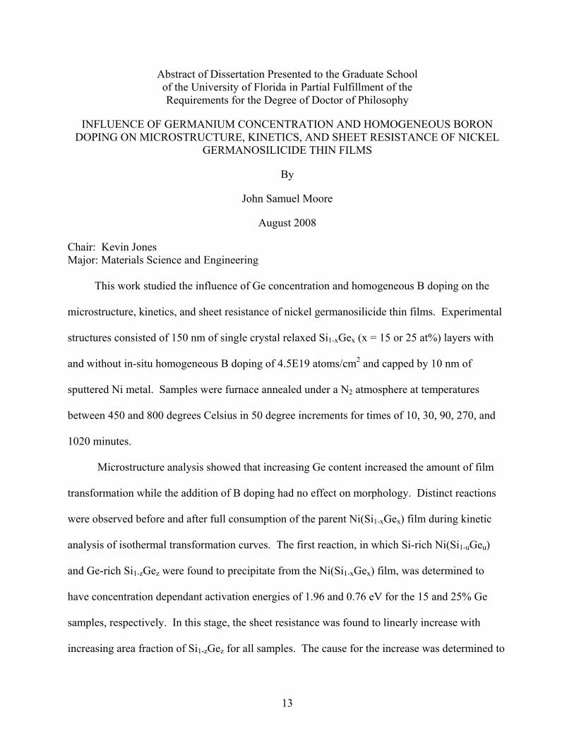
This work studied the influence of Ge concentration and homogeneous B doping on the
microstructure, kinetics, and sheet resistance of nickel germanosilicide thin films. Experimental
structures consisted of 150 nm of single crystal relaxed Si1-xGex (x = 15 or 25 at%) layers with
and without in-situ homogeneous B doping of 4.5E19 atoms/cm2 and capped by 10 nm of
sputtered Ni metal. Samples were furnace annealed under a N2 atmosphere at temperatures
between 450 and 800 degrees Celsius in 50 degree increments for times of 10, 30, 90, 270, and
1020 minutes.
Microstructure analysis showed that increasing Ge content increased the amount of film
transformation while the addition of B doping had no effect on morphology. Distinct reactions
were observed before and after full consumption of the parent Ni(Si1-xGex) film during kinetic
analysis of isothermal transformation curves. The first reaction, in which Si-rich Ni(Si1-uGeu)
and Ge-rich Si1-zGez were found to precipitate from the Ni(Si1-xGex) film, was determined to
have concentration dependant activation energies of 1.96 and 0.76 eV for the 15 and 25% Ge
samples, respectively. In this stage, the sheet resistance was found to linearly increase with
increasing area fraction of Si1-zGez for all samples. The cause for the increase was determined to
14
be related to the conductive path tortuosity. Increasing Ge content did not affect the
structure/property relationship, but the addition of B caused a decrease in sheet resistance. The
second reaction, in which Ni(Si1-uGeu) grains were found to agglomerate after the Ni(Si1-xGex)
layer was fully consumed, was determined to have an activation energy of 0.125 eV for both the
15 and 25% Ge samples. The undoped samples in this stage were found to have uniformly very
high sheet resistance values. This result was attributed to the lack of a conduction path between
isolated Ni(Si1-uGeu) grains. A strong linear relationship, however, was determined for the doped
samples, and increasing Ge content had a small effect on the relationship for these samples. It
was determined that the stabilizing influence of B doping was caused by the availability of a
conduction path through the unreacted doped Si1-xGex layer.
15
CHAPTER 1 INTRODUCTION
Nickel germanosilicides are formed when Ni metal and SiGe compounds react during
thermal processing. They are predominantly of interest to semiconductor technology where they
are used as an intermediate layer between devices and metal device interconnections. This work
investigates the influence of Ge content and in-situ B doping on the thermal stability of nickel
germanosilicides. The following sections in this chapter discuss why interconnections and
intermediate layers (silicides) are needed, why SiGe and in-situ B doping of the SiGe are used in
modern device designs, and why Ni metal is of interest as a silicidation metal.
1.1 Device Interconnections and Silicides
For modern microprocessor designs, tens of millions of individual transistors must be
linked together to form a single processor. The interconnections are made using complex,
interconnected, multi-layered patterns of metal. The metal must also be connected to the source,
gate, and drain contacts of each transistor. Direct contact, however, between the semiconductor
and the metal- such as that between Al and Si- can lead to the formation of Schottky barriers
which impede the flow of charge carriers. The height of the barrier depends upon the work
function difference between the semiconductor and the metal. Thus, barrier height is a function
of the materials selected and will vary from system to system. Regardless, Schottky barriers
degrade device performance by requiring electrons or holes to overcome an energy barrier as
they pass across the interface, raising overall circuit resistance and decreasing the time constant
(switching speed) of the device. The thermal stability of a metal-semiconductor interface may
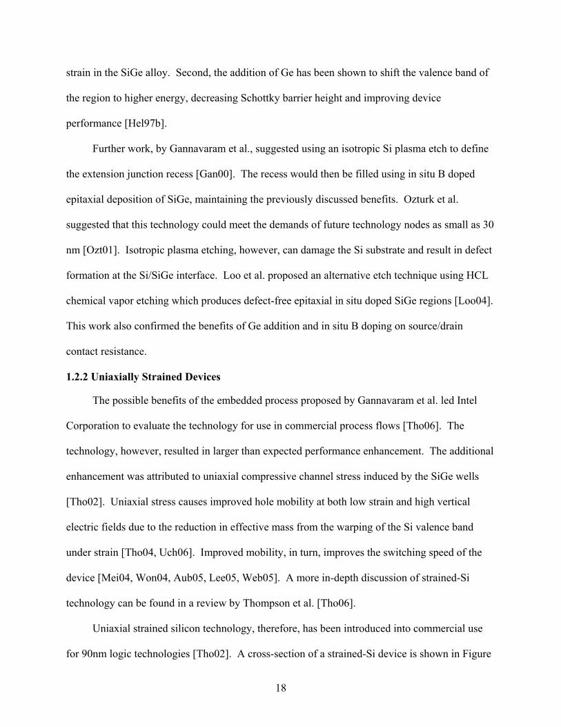
also be poor and lead to failure of the device. In the Al-Si system at 450-500 ºC, the solubility of
Si in Al is between 0.5 and 1.0 at% [Mey90]. As shown in Figure 1-1(a), Si therefore diffuses
16
from the substrate into the Al layer, creating pits in the silicon substrate. These pits, shown in a
Scanning Electron Microscopy (SEM) image in Figure 1-1(b), can disrupt device function.
Alternatively, an intermediate layer may be used to form low-resistance Ohmic contacts
(or Schottky contacts with known, lower, barrier heights) between the substrate, silicide, and
metal. Depending upon the materials selected, use of an intermediate layer can also result in
improved interface stability. To form the intermediate layer, a layer of metal is deposited onto a
semiconductor substrate where electrical contact is to be made. The metal, which is often
different that that used for interconnection, is then diffused into the substrate using a thermal
anneal. This results in the formation of a metal-semiconductor compound called, in the case of a
Si substrate, a silicide (alternatively, for a Ge substrate, a germanicide). Depending on the metal
and substrate, one or more stoichiometric compounds are possible, and more than one
stoichiometric compound may be initially formed.
One method of forming silicides is called a �“salicide�” (self-aligned silicide) process.
Figure 1-2 presents a simplified salicide process flow. The process flow begins once the
device�’s gate, source, drain, and SiO2 isolation has been fabricated. First, a metal layer is
uniformly deposited over entire structure, usually by a sputtering technique. Second, a thermal
anneal produces silicides at any metal/silicon interface. Metal not in contact with Si does not
react (hence the self-aligned nature of the technique). Once the silicide has been formed, the
remaining unreacted metal is removed using a selective etch.
Once formed, however, silicide layers (or germanicide, etc.) are subjected to additional
thermal processing during the remaining fabrication of the device. It is important, therefore, to
understand how the silicide may react or evolve due to subsequent thermal processing. For
example, when NiSi is annealed to temperatures above ~700 ºC a phase transformation from
17
NiSi to NiSi2 occurs and increases the resistance of the silicide [Gam98]. For other silicides,
such as TiSi2, additional thermal processing can cause the agglomeration of silicide grains that
also results in higher resistivity contacts [Gam98]. Thus, knowledge of the thermal stability of a
silicide is very important to process design.
1.2 Silicon-Germanium in Semiconductor Technologies
Silicon-Germanium (SiGe or, more specifically, Si1-xGex where x = at% Ge) are alloys of
varying atomic ratios of Si and Ge which are used in some semiconductor applications. The
properties of these alloys will be discussed in further depth in the following chapter. SiGe is
used for a variety of applications including photodiodes [Hua95], work-function-tunable gates
[Hel97, Pon00], and SiGe-channel heterojunction MOSFETs [Pea86, Ver94]. This work,
however, will focus on the use of SiGe in p-MOSFET logic technologies.
1.2.1 Low Resistivity Junctions
As critical device dimensions for MOSFET logic technology decreased below 130 nm,
new methods of forming shallow, low-resistance source/drain regions became necessary
[NTR97]. To overcome this problem, Raaijmakers et al. suggested the use of elevated
source/drain regions that would provide shallow junction depth and low sheet and contact
resistance [Raa99]. The raised regions, formed by selective epitaxial growth of in-situ B doped
Si above the contact region of the device, would also act as a sacrificial layer during silicidation.
Raaijmakers et al. also suggested that Ge should be added to the elevated source/drain region for
several reasons. First, the amount of electrically active B in SiGe alloys can be larger than that
in pure Si [Hel97b, Sal97, Man98]; higher concentrations of active dopant leads to lower contact
resistance to the silicide. In situ doping of the SiGe alloys also allows the elimination of an
activation anneal as most of the dopant is incorporated in substitutional positions (electrically
active) [Hel97b]. This effect, which is stable, is due to substitutional B compensating lattice
18
strain in the SiGe alloy. Second, the addition of Ge has been shown to shift the valence band of
the region to higher energy, decreasing Schottky barrier height and improving device
performance [Hel97b].
Further work, by Gannavaram et al., suggested using an isotropic Si plasma etch to define
the extension junction recess [Gan00]. The recess would then be filled using in situ B doped
epitaxial deposition of SiGe, maintaining the previously discussed benefits. Ozturk et al.
suggested that this technology could meet the demands of future technology nodes as small as 30
nm [Ozt01]. Isotropic plasma etching, however, can damage the Si substrate and result in defect
formation at the Si/SiGe interface. Loo et al. proposed an alternative etch technique using HCL
chemical vapor etching which produces defect-free epitaxial in situ doped SiGe regions [Loo04].
This work also confirmed the benefits of Ge addition and in situ B doping on source/drain
contact resistance.
1.2.2 Uniaxially Strained Devices
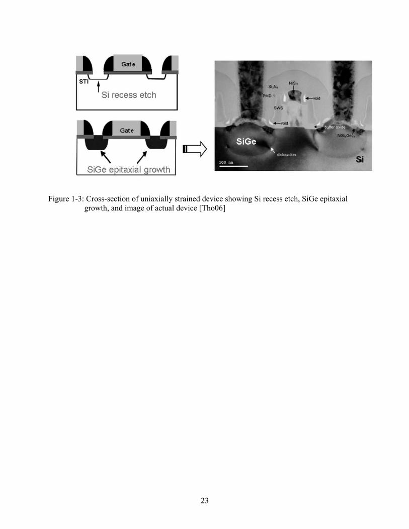
The possible benefits of the embedded process proposed by Gannavaram et al. led Intel
Corporation to evaluate the technology for use in commercial process flows [Tho06]. The
technology, however, resulted in larger than expected performance enhancement. The additional
enhancement was attributed to uniaxial compressive channel stress induced by the SiGe wells
[Tho02]. Uniaxial stress causes improved hole mobility at both low strain and high vertical
electric fields due to the reduction in effective mass from the warping of the Si valence band
under strain [Tho04, Uch06]. Improved mobility, in turn, improves the switching speed of the
device [Mei04, Won04, Aub05, Lee05, Web05]. A more in-depth discussion of strained-Si
technology can be found in a review by Thompson et al. [Tho06].
Uniaxial strained silicon technology, therefore, has been introduced into commercial use
for 90nm logic technologies [Tho02]. A cross-section of a strained-Si device is shown in Figure
19
1-3. While first-generation devices used ~17 at% Ge in the source/drain region, future
generation designs will likely increase the Ge concentration and bring the recessed region closer
to the channel [Bai04, Chi04, Tho06]. Additionally, by in situ doping of the SiGe region with B,
the benefits discussed in the previous section may be maintained.
1.3 Nickel as a Silicidation Metal
A number of metals have been researched as candidates for use as a silicidation metal for
both salicide and other processes. Table 1-1 presents important properties of silicides commonly
used in salicide processes. Both TiSi2 and CoSi2 have been used in commercially produced
products. TiSi2 has several benefits including low resistivity, relatively high thermal stability,
and the ability to reduce native oxides due to the high solubility of oxygen in Ti [Iwa85, Bar87
Mass90]. High temperature anneals (>800 ºC), however, are required to form the lowest
conductivity C54 phase. Even higher formation temperatures are reported to be required as
silicide thickness decreases, as linewidth decreases, and as the concentration on n-type dopants
increases [Las91, Gan93, Mae93].
An alternative silicide is CoSi2, which shares a similar resistivity and thermal stability to
TiSi2. The sheet resistance of CoSi2, however, is relatively insensitive to decreasing linewidth
[Las91, Mae93] and CoSi2 can be used as a dopant diffusion source to form shallow junctions
[Las91, Jia92a, Jia92b, Jia92c]. Disadvantages of CoSi2 in relation to TiSi2 include consumption
of more Si to produce an equivalent sheet resistance and the need for better surface preparation,
as CoSi2 does not reduce interfacial oxides. Though lower than that required for TiSi2, a
relatively high temperature anneal (600-800 ºC) is also required to form the lowest resistance
phase [Gam98].
A third option for a silicidation metal is Ni, forming NiSi. NiSi has a low resistivity, with
sheet resistance comparable to both of the previously discussed silicides. As with CoSi2, the

20
sheet resistance of the silicide is also relatively insensitive to linewidth. Furthermore, the
formation of NiSi requires less Si consumption than either TiSi2 or CoSi2 which allows the
formation of much shallower contacts [Gam98]. Finally, NiSi can be formed in a one-step
anneal at much lower temperatures (400-600 ºC) than either TiSi2 or CoSi2. Disadvantages of
NiSi include poor thermal stability including transformation to relatively high resistivity NiSi2 at
temperatures around 700 ºC. Further comparisons of NiSi, TiSi2, and CoSi2 are available in the
review articles by Gambino et al. [Gam98] and Iwai et al. [Iwa02].
1.4 Motivation of This Work
Individual transistors (and other devices) must be linked together to form a working unit
through the use of metal interconnections. The interconnections and the semiconductor substrate
can react, however, to form barriers to charge carrier flow and may also have poor thermal
stability. To prevent this, intermediate layers called silicides are used to decrease (or eliminate)
barrier height and improve interface stability. Most commonly, silicides are formed on the
source, drain, and gate regions of a semiconductor device through the use of a salicide process.
Recent developments in semiconductor technology suggest that the addition of Ge to the
source/drain contact regions of the device can provide increased dopant solubility and activation.
The use of embedded SiGe source/drain contacts also strains the channel of the device, leading to
additional performance gains. Due to a large number of benefits, there is also interest in the use
of nickel as a silicidation material. Thus, it is of particular interest to determine how the
introduction of Ge into the source/drain well will affect the Ni silicidation of these regions and to
determine if in situ B doping of the regions impacts the silicidation process. While investigation
of this topic has already begun (and will be discussed in the next chapter), questions remain
about the behavior of nickel germanosilicides. The motivation of this work, therefore, is to
answer some of these outstanding questions.
21
Figure 1-1: (a) Diagram showing diffusion of Si into Al and susbsequent pit formation in the Si substrate (b) SEM image of pits in Si substrate after removal of Al layer. [Mey90]

22
Figure 1-2: Salicide process flow (a) device with gate, source, drain, and SiO2 isolation fabricated (b) deposition of Ti layer over entire structure (c) thermal anneal under N2 ambient producing silicides at metal/silicon interfaces (cross-hatched regions) (d) device after selective etch to remove unreacted metal. [Gam98]
23
Figure 1-3: Cross-section of uniaxially strained device showing Si recess etch, SiGe epitaxial growth, and image of actual device [Tho06]

24
Table 1-1: Properties of common silicides used in salicide processing [Gam98].
25
CHAPTER 2 LITERATURE SURVEY
The ternary Ni-Si-Ge system includes three binary systems: Si-Ge, Ni-Si, and Ni-Ge.
Knowledge of the properties of the three binary systems will allow a deeper understanding of the
properties seen in the ternary. Thus, each of these four systems will be discussed in this chapter,
with emphasis on the microstructural evolution and electrical properties of the ternary system.
2.1 Binary Systems
2.1.1 Silicon-Germanium Binary System
The binary phase diagram of the Si-Ge system is shown in Figure 2-1. It can be seen from
this diagram that Si and Ge form a complete solid solution across all compositions of the alloy.
This is due to the satisfaction of the Hume-Rothery rules: the two elements share the same
diamond cubic crystal structure and valence state and have similar values of electronegativity
and atomic diameter. The properties of SiGe vary between those of Si and Ge. For some
properties, such as lattice parameter, the values vary linearly between that of Si and Ge in
accordance with Vegard�’s Law [Dis64]. For other properties, such as the melting point seen in
Figure 2-3, the relationship is nonlinear.
2.1.2 Nickel-Silicon Binary System
The binary phase diagram of the Ni-Si system is shown in Figure 2-2. Six intermediate
compounds are evident in the diagram ranging in composition from Ni-rich Ni3Si to Si-rich NiSi2
[Mey90]. Kinetically, however, only three compounds are of interest when Si is present in
excess amounts (as is the case during silicidation reactions): Ni2Si, NiSi, and NiSi2 [Gas98,
Nem06]. The evolution of these phases from the initial layers is shown schematically in Figure
2-3. Generally speaking, when a thin Ni layer is annealed in contact with excess Si the Ni2Si
phase forms until all Ni metal is consumed. This reaction begins around 210 oC [Nem06]. Once

26
all Ni metal has been consumed, the Ni2Si phase reacts with the Si substrate to produce NiSi.
These reactions are sequential; NiSi does not form until all Ni metal has reacted to form Ni2Si.
Experimental observation of the transitions are reported by Nemouchi et al. [Nem06] and shown
in Figure 2-4. Upon annealing above ~700 oC, NiSi transforms to NiSi2 [dHe82, dHe89]. While
other intermediate phases may appear during the reaction, the presence of these phases is
transient and usually neglected [Lav03, Ger04, Nem06]. The reaction rates of these
transformations (measured as a function of layer thickness) have been found to be proportional to
linear time (surface reaction controlled) or the square root of time (diffusion controlled)
[Mey90]. The formation of NiSi2 has also been found to be nucleation controlled [dHe84] and
Ni to be the dominant diffusing species for all phases [Fin81, dHe82, Mey90].
The electronic properties of the Ni-Si system are also of interest. Figure 2-5 presents the
sheet resistance of the system as a function of annealing temperature for three initial Ni layer
thicknesses as measured by Chen et al. [Che97]. All samples were annealed for 40 seconds.
Two observations can be determined from this plot. First, increasing the initial thickness of the
Ni layer increases the sheet resistance of the system for all temperatures. Second, three regimes
of sheet resistance are seen. These correspond to each of the three phases present in the
evolution of the Ni-Si system. Ni2Si, present at low temperature, and NiSi2, present at high
temperatures, both have sheet resistances higher than that of the intermediate NiSi phase
[Nem06]. For this reason, NiSi is the desired phase for semiconductor technology applications.
2.1.3 Nickel-Germanium Binary System
The phase diagram of the Ni-Ge system is shown in Figure 2-6; seven intermediate
compounds are evident in the diagram. As with the Ni-Si system, all of the phases in the
diagram are not seen experimentally. Unlike the Ni-Si system, however, some controversy exists
as to which phase initially forms during the reaction of Ni metal with excess Ge. Reported initial

27
phases include orthorhombic Ni2Ge [Hsi88, Li89], monoclinic Ni5Ge3 [Patt94], and hexagonal
Ni3Ge2 [Nem06]. Nemouchi et al. suggest that this confusion arises from the fact that the major
XRD diffraction lines are identical for all three of these phases [Nem06]. TEM/EELS analysis in
the same work showed the Ni5Ge3 phase to form first at a temperature around 140 oC.
Regardless, all of these authors agree that NiGe is the second and final phase formed in the
evolution of the films. Also unlike the Ni-Si system, the phases present in the thermal evolution
of the Ni-Ge system do not form sequentially [Nem06]. Instead, the initial N-rich phase (most
likely Ni5Ge3) and NiGe form simultaneously with the Ni-rich phase between that of the
unreacted Ni and NiGe. Once the Ni metal has been consumed, the Ni-rich phase transforms
into NiGe. This evolution is shown in Figure 2-7. It has been experimentally identified that Ni
is the diffusing species during the evolution of all phases [Tho88].
Figure 2-8 plots the sheet resistance of the Ni-Ge system as a function of annealing
temperature for two Ni layer thicknesses [Zha05]. A sample of Ni on Si was also included for
comparison. All samples were RTA processed for 30 seconds. It can be observed from this plot
that, as with the Ni-Si system, three regimes are present. At low temperature, the Ni-rich
germanicide has a higher sheet resistance than the NiGe phase present at intermediate
temperatures. At higher temperatures (~500-600 oC), a rapid increase in sheet resistance is
apparent. Unlike the Ni-Si system, this increase is not attributed to phase transformation as
NiGe2 has only been reported to form at high temperatures and pressures [Tak00]. Instead, this
rapid increase in sheet resistance is due to the agglomeration of NiGe which has been shown to
begin at temperatures as low as 400 oC [Zha05].
28
2.2 Ternary System: Ni-Si-Ge
2.2.1 Physical Properties
When Ni is reacted with SiGe, a ternary alloy of Ni, Si, and Ge is formed. While the
composition of the Ni-rich initial phase is a matter of some debate [Cha04, Zha02], it is agreed
that the silicidation process produces Ni(Si1-xGex) with the ratio of Si to Ge identical to that of
the silicided Si1-xGex alloy at temperatures around 400 oC [Zha02, Cha04, Liu05]. Since both
NiSi and NiGe have the same space group (pnma) and prototype crystal (MnP) [Mas90] and Si
and Ge form a complete solid solution, it is thought that Ni(Si1-xGex) is a complete solid solution
of NiSi and NiGe in the appropriate ratio [Seg02]. It has also been shown that the formation of
NiGe2 is limited to high temperatures and pressures not seen during silicidation processing
[Tak00]. Exhaustive experimental evidence has furthermore shown that small quantities of Ge
(~1 at% +) prevents the formation of NiSi2 at temperatures up to 800 oC or more [Jar02, Seg02,
Ish03, Seg03], most likely due to the lack of the corresponding NiGe2 phase. Several of these
authors have therefore proposed that Ni(Si1-xGex) will not transform to Ni(Si1-xGex)2 and at this
date no experimental evidence has been shown to the contrary for annealing temperatures up to
850 oC for 30 seconds [Jar02].
2.2.2 Phase Diagram
S.-L. Zhang performed a series of thermodynamic calculations treating Ni(Si1-xGex) as a
complete solid solution of NiSi and NiGe [Zha03]. If the Ni(Si1-xGex) layer is in contact with
Si1-xGex, as is usually the case in silicidation, the equilibrium minimum free energy of the Ni(Si1-
xGex)-Si1-xGex system can be calculated with this method. The graphical results for an example
calculation with one gram-atom of Ni(Si0.5Ge0.5) in contact with one gram-atom of Si0.5Ge0.5 at
600 oC is presented in Figure 2-9. From this graph, it can be determined that the system will
reach equilibrium with one gram-atom of Ni(Si0.90Ge0.10) and one gram-atom of Si0.30Ge0.70
29
[Zha03]. The driving force for the rejection of Ge from the nickel germanosilicide is the
difference in the heats of formation for NiSi (-45 kJ/gram-atom) and NiGe (-32 kJ/gram-atom)
[45 from Zha06].
Using similar methodology, partial isotherms for the ternary phase diagram can be
calculated. Examples of calculated isotherms are shown in Figure 2-10. The horizontal line
between NiSi and NiGe represents all possible compositions of the complete solid solution (any
composition of Ni(Si1-xGex). It should be noted that the presence and behavior of Ni-rich phases
(e.g. Ni2Si and Ni5Ge3) are neglected and not shown. As mentioned previously, the presence of
Ge has been shown to severely inhibit the formation of NiSi2. Eliminating NiSi2 from the
calculations produces the isotherms shown in Figure 2-11. This change affects only nickel
germanosilicides with very small concentrations of Ge (x< ~0.05) and it has been suggested that
confirmation of this change may be difficult [Jar02]. For the previous example of NiSi0.5Ge0.5 in
contact with Si0.5Ge0.5, use of either 600 oC isotherm, shown in Figure 2-12 for the modified
calculations, indicates the resulting equilibrium states of NiSi0.9Ge0.1 and Si0.3Ge0.7.
2.2.3 Microstructure
Knowledge of the microstructure of Ni(Si1-xGex) and its thermal stability is important to
determine the possible processing window of the material. While no transformation to a high-
resistance digermanosilicide analogous to NiSi2 has been reported in literature, nickel
germanosilicide films have relatively poor thermal stability due to the thermodynamic impetus
for Ge rejection as calculated by Zhang. Thus, many researchers have investigated the
microstructure of Ni(Si1-xGex) and its thermal evolution over a range of processing conditions.
The results from these investigations will be discussed in the following sections.
30
2.2.3.1 Initial film formation
The initial reaction of a Ni metal layer with a Si1-xGex alloy produces a Ni-rich phase
analogous to the Ni-rich Ni2Si and Ni5Ge3 phases reported for the Ni-Si and Ni-Ge systems,
respectively. For a 325 oC 30 second anneal, this phase has been reported to be Ni2(Si1-xGex) by
Chamirian et al. [Cha04]. For a 300 oC 60 second anneal the presence of both Ni2(Si1-xGex) and
Ni3(Si1-xGex)2 has been reported by Zhao et al.[Zha02]. The existence of Ni2Si, Ni2Ge, Ni3Si2
and Ni3Ge2 are all reported on the respective phase diagrams and so solid solutions of either pair
seem reasonable. Further information on Ni-rich phase formation is not available in literature at
this time; one or both phases may form sequentially or simultaneously or other intermediate
phases may also occur.
Regardless of the composition and evolution of the initial Ni-rich phase, on annealing to
temperatures at 450 oC for 30 seconds, and as high as 700 oC for 30 seconds, Chamirian et al.
and Zhao et al. both report that the Ni-rich phase disappears and Ni(Si1-xGex) predominates for
all samples. XRD spectra confirming the sole presence (disregarding SiGe and Si peaks) of
Ni(Si1-xGex) at temperatures over 400 oC and ranging as high as 800 oC have been reported by
several additional authors [Liu04, Ok04, Pey02, Cho06, He05, Yao07]. One set of XRD spectra
containing this evolution is included in Figure 2-13. Since Ni(Si1-xGex) is the phase of interest
for use as an intermediate silicide layer in semiconductor applications, most work on nickel
germanosilicides has therefore focused on thermal anneals at temperatures higher than 400-500
oC where no Ni-rich nickel germanosilicide forms.
Ni(Si1-xGex) films formed by annealing at temperatures from 400-450 oC and times of 30-
60 seconds on crystalline Si1-xGex substrates (with x ranging from 10 to 20 at % Ge) have been
analyzed with XTEM/EDS by several authors [Zha02, Jon04, Ok04, Ko06, Yao07]. These
authors all agree that Ni(Si1-xGex) films produced in this annealing range have homogeneous

31
compositions with Si to Ge ratios identical to that of the Si1-xGex substrate. The films are also
shown in these works to be granular, continuous, and of uniform thickness. XTEM images of
representative films formed within this range are shown in Figure 2-14.
2.2.3.2 Film agglomeration
As shown by the previously discussed thermodynamic calculations of Zhang [Zha06], the
uniform Ni(Si1-xGex) films produced at temperature ranges from 400-450 oC are not
thermodynamically stable when in contact with unreacted Si1-xGex. Instead, at longer times or
elevated temperatures, nickel germanosilicide films undergo Ge rejection and form Si1-zGez
grains that are Ge-rich relative to the Si1-xGex substrate (z > x) interspersed between remaining
Si-rich Ni(Si1-uGeu) grains (u < x). This process has been experimentally observed by a large
number of researchers [Pey02, Zha02, Pey04, Jin05, Yao07]. Furthermore, the equilibrium
concentrations of the Ni(Si1-uGeu) and Si1-zGez grains predicted by Zhang�’s ternary isotherms
have been shown to be in good agreement with observed experimental values [Pey04]. While
the overall process of the rejection of Ge and the formation of Si1-zGez is commonly referred to
in literature as �“agglomeration�” of the germanosilicides, it would be more accurate to label the
process as an eutectoid-type solid state phase transformation.
The initial stages of the transformation have been observed by Yao et al. for samples with
20 at% Ge annealed at 500 oC for 20 seconds [Yao07]. Using HRXTEM, the researchers
observed sharp v-shaped grooves forming at the intersection of Ni(Si1-xGex) grain boundaries and
the Ni(Si1-xGex)/ Si1-xGex. One such groove is shown in Figure 2-15(a). Similar grooving is also
observed in NiSi and NiGe samples; examples of these grooves are shown in Figure 2-15 (b) and
(c), respectively. The grain boundary angles, indicated as in the figures, was found to be
smaller in the germanosilicide than in the silicide or germanide. The overall shape of the
interfaces in the germanosilicide was also found to be more planar. These findings led Yao et al.

32
to suggest that grooving occurs much more rapidly in the germanosilicide and sufficient time is
not available to diffusively smooth the interfaces. Yao et al. also performed EDS on the
HRXTEM samples to determine the distribution of Ge in the vicinity of the grain
boundary/groove. The results, shown in Figure 2-15(d), indicate that the grain boundary above
the groove is depleted of Ge while the region immediately below the groove is enriched in Ge.
These findings suggest that Ge rejection occurs along the grain boundaries of the Ni(Si1-xGex)
grains.
Later stages of the transformation have been observed by a number of researchers [Zha02,
Pey02, Ok03, Pey04, Jin05]. In these studies, with Ge compositions ranging from 20 to 25 at %,
anneal temperatures ranging from 500 to 800 oC, and anneal times ranging from 30 to 60
seconds, XTEM analysis shows Ge-rich Si1-zGez grains have formed between grains of Si-rich
Ni(Si1-uGeu) [Ok03, Pey04]. One representative set of XTEM images, from Pey et al. [Pey04] is
shown in Figure 2-16. At lower temperatures (500 to 700 oC, Figure 2-16 (a)-(c)), distinct Ge-
rich Si1-zGez grains are distinguishable in the film. The number and spacing of Si1-zGez grains is
also observed to increase in this range. While not explicitly discussed in any of the works, misfit
dislocations can be noted between the Si1-zGez grains and the Si1-xGex layer. These results, when
combined with the observations of Yao et al., suggest that in this annealing range the Ge-rich
regions below the grooved grain boundary form Ge-rich Si1-zGez grains which are distinct from
the Si1-xGex layer. At higher temperatures (~800 oC, Figure 2-16(d)), the misfit dislocations
between the grains and the layer are not observed, suggesting that the Ge concentration gradient
may have lessened due to diffusion. The spacing between Ni(Si1-uGeu) grains is also larger in
this temperature range.
33
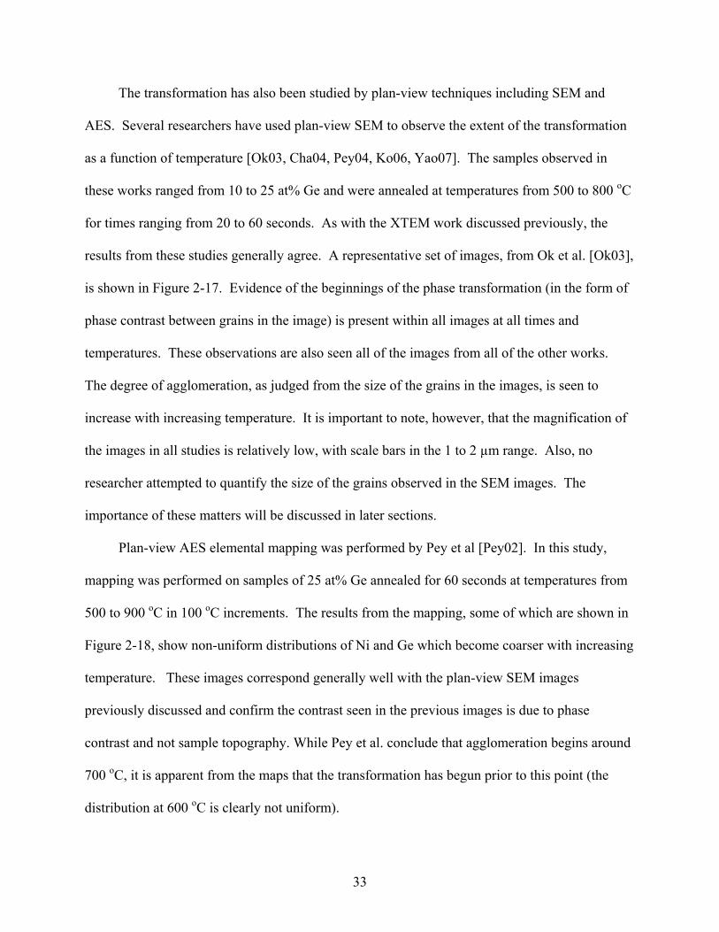
The transformation has also been studied by plan-view techniques including SEM and
AES. Several researchers have used plan-view SEM to observe the extent of the transformation
as a function of temperature [Ok03, Cha04, Pey04, Ko06, Yao07]. The samples observed in
these works ranged from 10 to 25 at% Ge and were annealed at temperatures from 500 to 800 oC
for times ranging from 20 to 60 seconds. As with the XTEM work discussed previously, the
results from these studies generally agree. A representative set of images, from Ok et al. [Ok03],
is shown in Figure 2-17. Evidence of the beginnings of the phase transformation (in the form of
phase contrast between grains in the image) is present within all images at all times and
temperatures. These observations are also seen all of the images from all of the other works.
The degree of agglomeration, as judged from the size of the grains in the images, is seen to
increase with increasing temperature. It is important to note, however, that the magnification of
the images in all studies is relatively low, with scale bars in the 1 to 2 µm range. Also, no
researcher attempted to quantify the size of the grains observed in the SEM images. The
importance of these matters will be discussed in later sections.
Plan-view AES elemental mapping was performed by Pey et al [Pey02]. In this study,
mapping was performed on samples of 25 at% Ge annealed for 60 seconds at temperatures from
500 to 900 oC in 100 oC increments. The results from the mapping, some of which are shown in
Figure 2-18, show non-uniform distributions of Ni and Ge which become coarser with increasing
temperature. These images correspond generally well with the plan-view SEM images
previously discussed and confirm the contrast seen in the previous images is due to phase
contrast and not sample topography. While Pey et al. conclude that agglomeration begins around
700 oC, it is apparent from the maps that the transformation has begun prior to this point (the
distribution at 600 oC is clearly not uniform).

34
2.2.4 Sheet Resistance
One commonly studied electrical property of nickel germanosilicide films is sheet
resistance, likely due to the ease of measurement via four point probe analysis. Sheet resistance
is measured in Ohms/sq and, given the thickness of the film, the resistivity of the film can be
extracted from the value. Ok et al. performed an experiment where the sheet resistance of nickel
germanosilicide films was measured as a function of annealing temperature [Ok03]. The
structures used in the study were comprised of 25 nm of Ni deposited on Si1-xGex films with 0,
10, and 20 at% Ge and samples were annealed for 30 seconds. The measurements from the
study are presented in Figure 2-19. Below 600 oC, the sheet resistance of each film is stable.
Above this temperature, the sheet resistance of all sample conditions increases with increasing
temperature (the difference in values between the samples as a function of Ge content will be
discussed later). For the samples with 0 at% Ge (Ni on Si), the increase is attributed to the
previously discussed transformation of NiSi to higher resistance NiSi2 around 700 oC. The Ni-
Si-Ge system, however, was previously shown to lack a corresponding high resistance
digermanosilicide. Thus, the increase of sheet resistance for the nickel germanosilicide
structures was attributed to the agglomeration (decomposition) of the film. Similar results and
conclusions have been presented by a number of researchers [Pey02, Zha02, Cha04, Cha04b,
Zha04, Seg04, Liu05, Cho06, Ko06, Lau06, Yao06].
2.2.5 Influential Variables
Several variables have been determined to be influential in the stability and evolution of
nickel germanosilicide thin films. These variables include the strain state, thickness, Ge content,
thickness, and crystalline quality of the Si1-xGex layer and the thickness of the Ni layer. The
impact of doping via both implantation and in-situ methods has also been studied. The following
35
sections briefly discuss the most important variables and their impact on the films, both in terms
of microstructure and sheet resistance.
2.2.5.1 Silicon-germanium layer strain and thickness.
Zhao et al. performed a study using XTEM analysis to determine if the strain state (prior to
silicidation) of the Si1-xGex layer impacted the stability of the films [Zha04]. The study used
structures with a Si0.73Ge0.27 layer which was partially relaxed (50 or 75%) for some samples
prior to deposition of 20 nm of Ni metal. Samples were then annealed at temperatures from 400-
650 oC for 60 seconds. The authors concluded that increasing layer strain enhanced
agglomeration due to an increase in interface energy. This conclusion, however, is not well-
supported by the XTEM images presented by the authors as no distinct morphological difference
is evident in the images. Plan-view analysis of the samples was not performed. The authors also
noted that, for fully-strained layers annealed at 600 oC for 60 seconds, misfit and threading
dislocations formed at the Si1-xGex/Si interface in locations where germanosilicide grains
approached the interface. These results suggest that the depth of the silicidation may affect strain
relaxation of the Si1-xGex layer. In conjunction with the authors�’ conclusion that increasing layer
strain increases agglomeration, this suggests that the proximity of the germanosilicide layer to
the Si1-xGex/Si may affect agglomeration behavior.
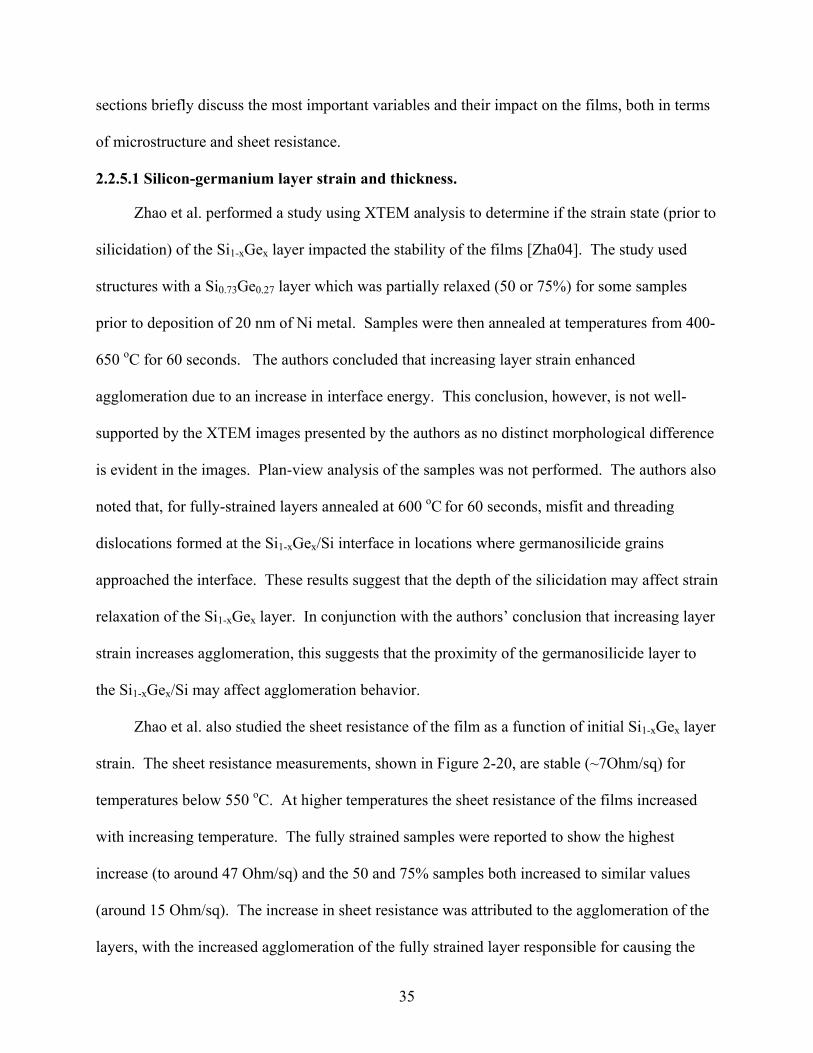
Zhao et al. also studied the sheet resistance of the film as a function of initial Si1-xGex layer
strain. The sheet resistance measurements, shown in Figure 2-20, are stable (~7Ohm/sq) for
temperatures below 550 oC. At higher temperatures the sheet resistance of the films increased
with increasing temperature. The fully strained samples were reported to show the highest
increase (to around 47 Ohm/sq) and the 50 and 75% samples both increased to similar values
(around 15 Ohm/sq). The increase in sheet resistance was attributed to the agglomeration of the
layers, with the increased agglomeration of the fully strained layer responsible for causing the

36
highest increase of sheet resistance. No direct relationship between agglomeration and sheet
resistance was established.
2.2.5.2 Germanium content of Si1-xGex layer.
Ok et al. used plan view SEM to establish the effect of increasing the Ge content in the Si1-
xGex film on germanosilicide formation and stability [Ok03]. Images from the study are shown
in Figure 2-21 for samples with Si1-xGex compositions of 10 and 20 at% Ge annealed at 650, 700,
and 750 oC for 30 seconds. The authors noted that the surface of the samples with increased Ge
content showed a qualitatively greater number of dark regions (corresponding to areas of Si1-
xGex uncovered by the phase transformation) when compared to the images of samples with
lower Ge content and identical anneals. From these observations, it was concluded that
increasing Ge content caused the germanosilicide to become degraded at lower temperatures. No
quantitative study of the images, however, was performed. Careful examination of the images
also reveals evidence of non-uniform contest for both samples annealed at 650 oC, the lowest
temperature shown. This observation suggests that the reaction has already begun for these
samples.
As previously shown in Figure 2-19, Ok et al. also measured the sheet resistance of the
samples used in the study. The measurements showed that the magnitude of the sheet resistance
in the stable region (anneal temperature less than 700 oC) increased with increasing Ge content in
the initial Si1-xGex layer. No explanation for this behavior was presented in the work. The
measurements also showed that, once sheet resistance began to increase at higher temperatures,
the sample with larger Ge content increased more rapidly. Though no direct relationship was
established, the increases were again attributed to agglomeration of the films at higher
temperatures; the greater increase in sheet resistance of the higher concentration Ge sample was
ascribed to the increased agglomeration seen in those samples.
37
While the previously discussed work by Zhao et al. [Zha04] only studied the
microstructure evolution for Ni-silicided Si0.73Ge0.27 layers with various levels of initial strain,
the study also measured the sheet resistance of identically processed samples with Si0.81Ge0.19
layers. All samples showed an increase in sheet resistance beginning around 550 oC, once more
attributed to film agglomeration. The sheet resistance measurements of the films with higher
initial Ge content, however, were shown to increase more than those with lower concentrations
for each strain condition. The difference was credited to increased agglomeration in the samples
with higher initial Ge content in the Si1-xGex film. This conclusion, while in agreement with the
conclusions of Ok et al., was not supported by microstructure analysis of the lower concentration
samples. Additionally, no direct relationship between microstructure and sheet resistance was
determined.
2.2.5.3 Crystalline quality of the Si1-xGex layer.
The works previously discussed in this literature survey have all used single-crystal Si1-
xGex layers as the basis for germanosilicide layer formation. The formation of germanosilicide
layers on poly-crystalline Si1-xGex layers, however, has also been studied and found to exhibit
significantly different behavior. Using XTEM/EDS analysis, Jarmar et al. have shown that, as
with nickel germanosilicide layers formed on single-crystal Si1-xGex layers, those formed on
poly-crystalline Si1-xGex layers also initially form a continuous Ni(Si1-xGex) layer that rejects Ge
and agglomerates [Jar02]. A notable difference, however, is that the Ni-rich Ni(Si1-uGeu) grains
were shown to be much more mobile and migrated to the wafer surface and Si1-xGex/Si interface.
Thus, it can be concluded that the quality of the Si1-xGex layer can clearly affect the evolution of
the nickel germanosilicide layer. No sheet resistance measurements were included in the study.

38
2.2.5.4 Nickel layer thickness.
The influence of the thickness of the initial Ni layer on germanosilicide film evolution has
been studied by Ko et al. [Ko06]. In the work, two thicknesses of Ni metal (11 and 21 nm) were
deposited on samples of relaxed Si0.75Ge0.25 and germanosilicides were formed using a two-stage
anneal. Samples were first annealed at 400 oC for 60 seconds to form a homogeneous
Ni(Si0.75Ge0.25) layer. The samples were then annealed at 750 oC for an unreported time. One
annealed, the samples were images with FE-SEM in BSE mode. The images, not included here
due to their poor quality, show that the grain size of the samples with the thicker Ni layer was
qualitatively larger than those of with the thinner Ni layer. Since a thicker initial Ni layer will
produce a thicker nickel germanosilicide film (as more Ni is available to react), these results
suggest that the thickness of the germanosilicide may affect the stability and evolution of the
film. No quantification of the different morphologies was attempted.
The study by Ko et al. also investigated the effect of varying the initial Ni layer thickness
on the sheet resistance of the layers as a function of annealing temperature. The samples and
thermal processing used in this portion of the study were identical to those previously discussed
with the exception of either 11 or 21 nm of Ni being deposited prior to silicidation. The
measurements show that increasing the thickness of the Ni layer did not affect sheet resistance
(stable at ~ 5-10 Ohm/sq) for any sample at temperatures below 600 oC. Between 600 to 650 oC,
samples with the thinner initial Ni layer showed an abrupt rise in sheet resistance to around 75
Ohm/sq. The sheet resistance of these samples was then stable (at ~75 Ohm/sq) to temperatures
as high as 800 oC. In contrast, samples with the thicker Ni layer showed only a gradual increase
in sheet resistance above 600 oC, with a maximum value of ~75 Ohm/sq reached at 800 oC. The
difference in behavior was attributed to two causes. First, the increased availability of Ni in the
films formed from thicker Ni layers produces thicker germanosilicide layers and thus decreases
39
sheet resistance. Second, the samples with thicker initial Ni layers displayed a larger grain size
after annealing, causing an increase in film interconnectivity and thus a more stable sheet
resistance. More simply, increasing Ni thickness decreased agglomeration and thus lowered
sheet resistance. Again, no attempt to directly link the two properties was made.
Liu and Ozturk also varied the initial Ni layer thicknesses (10 and 20 nm) in a study using
fully relaxed Si1-xGex layers with Ge concentrations greater than 40% with and without in-situ B
doping [Liu05]. The effect of B doping will be discussed later. No comparative microstructure
analysis of the samples with varying initial Ni layer thickness was made, however the sheet
resistance of the samples was measured as a function of temperature for 30 second anneals. The
results from the experiment, shown in Figure 2-22, show that the samples with thicker Ni layers
had lower sheet resistance measurements at all temperatures. For the undoped samples, the
samples with the thicker initial Ni layer did not show an increase in sheet resistance until ~450
oC while the samples with the thinner layer started to display and increase around 350 oC. These
results agree well with those found by Ko et al. and were attributed to the same factors: thicker
and more stable germanosilicide layers produced by the increased initial thickness of Ni.
2.2.5.5 Implanted Dopants.
Chamirian et al. studied the effect of implanting Si1-xGex films with dopants prior to Ni
deposition and germanosilicide formation [Cha04]. In the study, both single- and poly-
crystalline films of Si0.8Ge0.2 were ion implanted with either As (4 x 10¹⁵ atoms/cm2, 20 keV) or
B (2 x 10¹⁵ atoms/cm2, 2 keV). Next, a spike anneal to 1100 oC was performed to activate the
dopants prior to deposition of 10 nm of Ni metal. Samples were then annealed at 450 oC for 30
seconds to produce a Ni(Si0.8Ge0.2) film. To study the thermal stability, the samples were
annealed a second time at temperatures of 450, 600, and 700 oC for 30 seconds. Plan view SEM
images of the films formed on single-crystal Si1-xGex substrates are shown in Figure 2-23. No

40
quantitative analysis of the images was performed. Qualitatively, however, the morphology of
the films does not appear to differ between the As and B implanted films (no non-implanted
control samples were included in the study). Plan view SEM images of the films formed on
polycrystalline substrates were also included in the work, though they are not reproduced here.
These images also showed no qualitative difference in film morphology between the
corresponding As and B implanted samples, though the overall grain size of the films appeared
to be smaller than those formed on the single-crystal layers.
The sheet resistance of the samples used in the study by Chamirian et al. was also
measured. These measurements, presented in Figure 2-24, show no significant difference
between the As and B doped samples for the films formed on either single- or poly-crystalline
Si1-xGex layers. The plateau at temperatures below ~375 oC was attributed to the Ni-rich
germanosilicide phases present at these temperatures having a higher resistivity than the Ni(Si1-
xGex) phase previously shown to be present at temperatures greater than around 400 oC. The
increase in sheet resistance seen around 600 oC for all samples was attributed to the
agglomeration of the film. The similarity in sheet resistance between the As and B doped
samples was attributed to the previously discussed similarity in the morphology of the films. No
quantitative relationship between sheet resistance and film morphology was established in the
study.
2.2.5.6 In-situ Doping.
The impact of heavily doping the Si1-xGex layer during its epitaxial growth (in-situ doping)
on germanosilicide stability was studied by Liu and Ozturk [Liu05]. In the work, fully relaxed
Si1-xGex layers with Ge concentrations greater than 40% were doped with approximately 2 at% B
(1x 10²¹ atoms/cm2). Undoped samples with identical Ge concentration were also grown for
comparison. A 20 nm thick layer of Ni was then deposited and the samples were annealed at

41
temperatures from 300 to 750 oC for 30 seconds to form nickel germanosilicide films. SIMS
analysis of the B-doped sample annealed at 500 oC showed the formation of a shoulder and
significantly longer tail for the Ni distribution when compared to the analysis of the B-doped
sample annealed at 450 oC. It should be noted that the SIMS analysis was reported as a plot of
analysis time vs. counts and was not converted to depth vs. concentration. Regardless, this
change was attributed to significant interface roughening. The Ni(Si1-xGex)/Si1-xGex interface
was further studied by selectively etching the germanosilicide and performing Atomic Force
Microscopy (AFM) analysis of the exposed interface. Table 2-1 presents the average interface
roughness values for doped and undoped samples annealed at 400 and 500 oC. The average
roughness of the doped samples is significantly less than that of the undoped samples at each
temperature. Liu and Ozturk attributed these results to the high levels of boron doping
decreasing agglomeration through strain compensation. This theory is supported by the well-
established ability of boron doping to compensate strain in Si1-xGex films at concentrations lower
than 1 at% [Cho06a, Cho06b] and the previously discussed conclusions of Zhao et al. [Zha06]
who stated that increasing strain increased the amount of film degradation. Other work has
determined a similar effect in nickel germanosilicide samples highly doped with C [Tol04].
The sheet resistance of the samples used in the experiment by Liu and Ozturk was also
measured as a function of anneal temperature. The measurements, previously shown in Figure 2-
22, indicate that the addition of the in-situ B doping stabilized the sheet resistance of the films
above 350 and 450 oC for the samples with 10 and 20 nm thick initial Ni layers, respectively.
While the sheet resistance of the samples with B-doped Si1-xGex layers continues to gradually
increase with increasing temperature, a sharp rise in the property is not seen. The stabilization
42
was attributed by Liu and Ozturk to their conclusion that the heavy B doping reduced the
agglomeration of the films.
2.3 Outstanding Issues
While a substantial amount of work has been accomplished with the intent of
understanding the formation and stability of nickel germanosilicide films, a number of questions
remain unanswered in literature. First, can a direct relationship between film agglomeration and
the increase in sheet resistance be established? While many works have proposed a qualitative
link between the two properties, no quantitative relationship has been put forth. Without the
establishment of a direct, quantitative relationship the connection between the two properties
cannot be absolutely established. Second, does the addition of high levels of B doping truly
affect the amount of agglomeration in nickel germanosilicide films? The study by Liu and
Ozturk utilized only indirect measurement techniques during their investigation of the
morphology of the films. If there is indeed an effect, does any quantitative relationship between
agglomeration and sheet resistance still hold true? If there is not an effect, what is then causing
the stabilization of sheet resistance in the films? Finally, the studies available in literature all
utilize isochronal experiments with very short annealing times. What happens if the experiments
are performed over a larger range of time and temperatures? Answers to these questions will
further clarify the behavior of nickel germanosilicide thin films.
43
Figure 2-1: Binary phase diagram of Si-Ge system showing complete solid solubility of Si and Ge in the solid phase [Mas90].
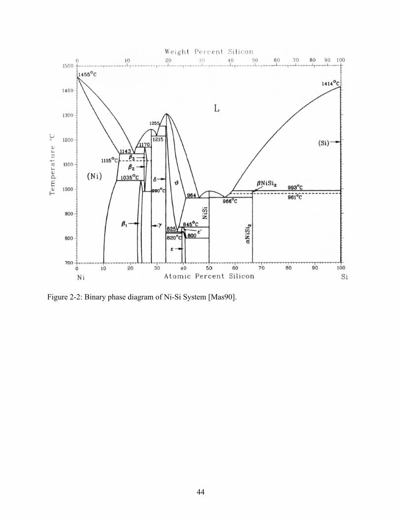
44
Figure 2-2: Binary phase diagram of Ni-Si System [Mas90].

45
Figure 2-3: Schematic of the evolution of Ni-Si binary system on thermal annealing. The right hand path (excess Si, Ni layer consumed) is followed for silicidation processes [Mey90]

46
Figure 2-4: XRD results plotting the squared normalized intensity of characteristic diffraction peaks for Ni, Ni2Si, and NiSi as a function of anneal time. Samples were 50 nm of Ni on a-Si substrate annealed at 230 oC. Note that the Ni signal disappears prior to the appearance of NiSi [Nem06].
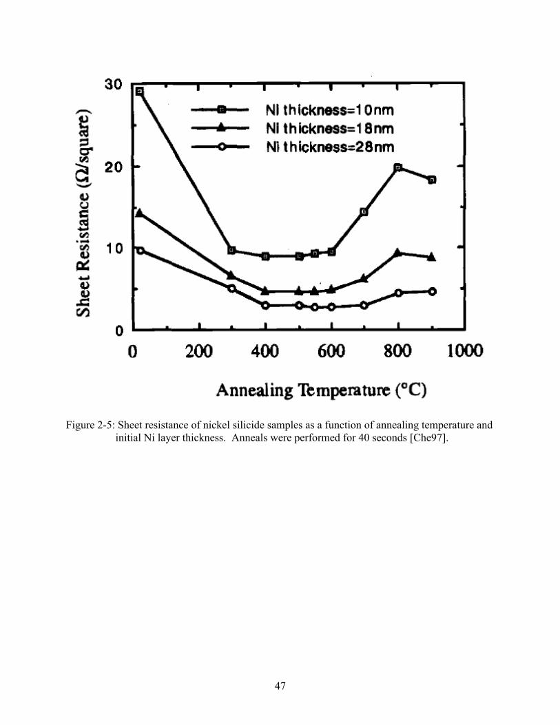
47
Figure 2-5: Sheet resistance of nickel silicide samples as a function of annealing temperature and initial Ni layer thickness. Anneals were performed for 40 seconds [Che97].
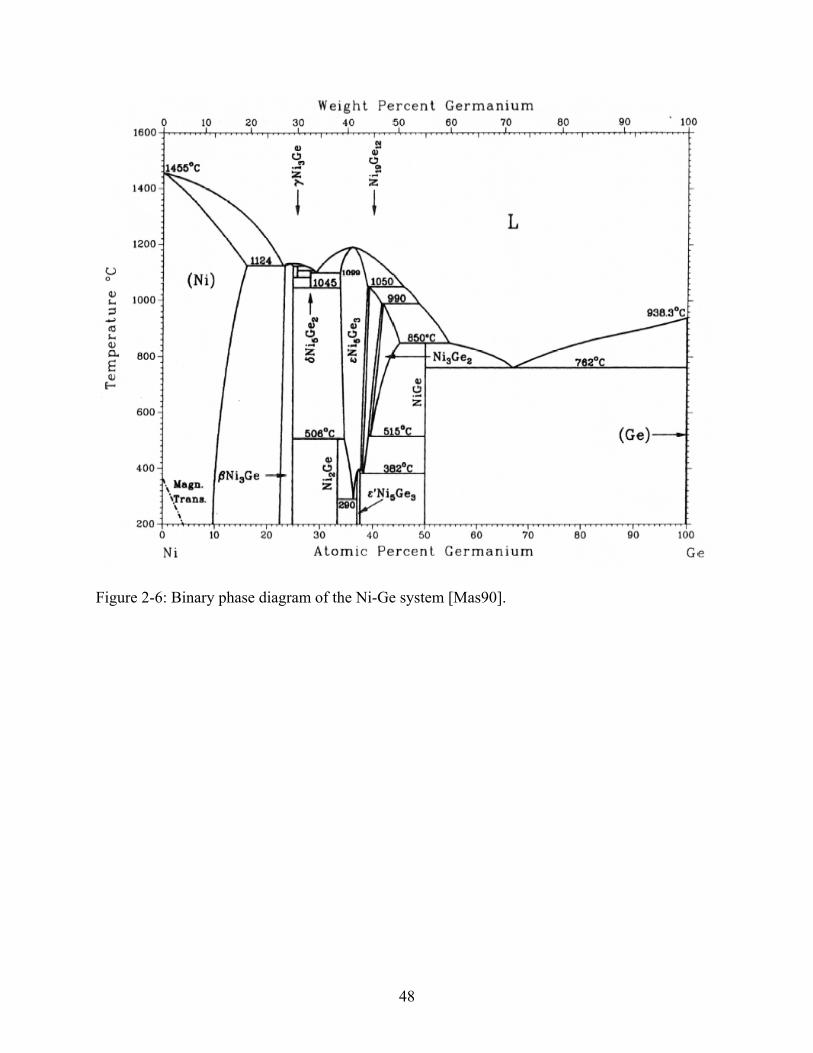
48
Figure 2-6: Binary phase diagram of the Ni-Ge system [Mas90].
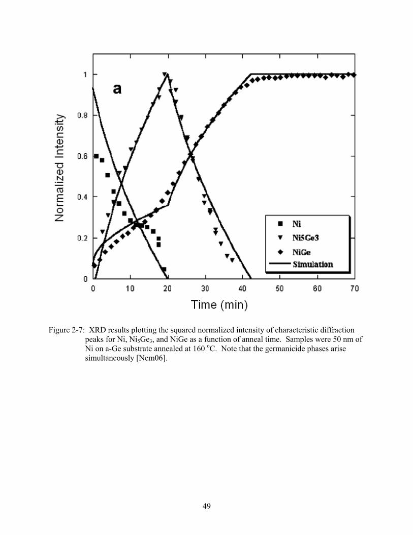
49
Figure 2-7: XRD results plotting the squared normalized intensity of characteristic diffraction peaks for Ni, Ni5Ge3, and NiGe as a function of anneal time. Samples were 50 nm of Ni on a-Ge substrate annealed at 160 oC. Note that the germanicide phases arise simultaneously [Nem06].

50
Figure 2-8: Sheet resistance of Ni-Ge system as a function of annealing temperature for two initial Ni layer thicknesses. Sheet resistance of Ni on Si is also shown for comparison. All samples were annealed for 30 seconds [Zha05].
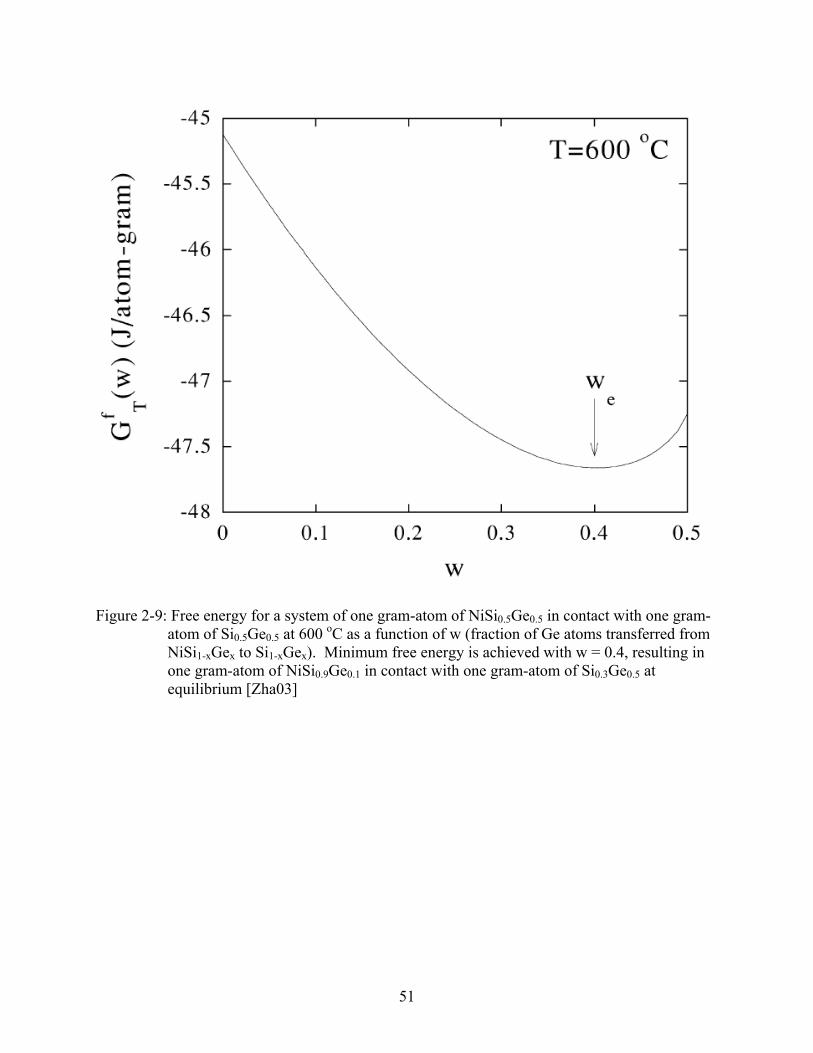
51
Figure 2-9: Free energy for a system of one gram-atom of NiSi0.5Ge0.5 in contact with one gram-atom of Si0.5Ge0.5 at 600 oC as a function of w (fraction of Ge atoms transferred from NiSi1-xGex to Si1-xGex). Minimum free energy is achieved with w = 0.4, resulting in one gram-atom of NiSi0.9Ge0.1 in contact with one gram-atom of Si0.3Ge0.5 at equilibrium [Zha03]

52
Figure 2-10: Partial isotherms calculated for the Ni-Si-Ge ternary system for (a) 600 oC and (b) 750 oC. Note that the presence and behavior of Ni-rich phases (e.g. Ni2Si, Ni5Ge3) are neglected [Jar02]

53
Figure 2-11: Partial isotherms calculated for the Ni-Si-Ge ternary system without inclusion of the NiSi2 phase for (a) 600 oC and (b) 750 oC [Jar02]
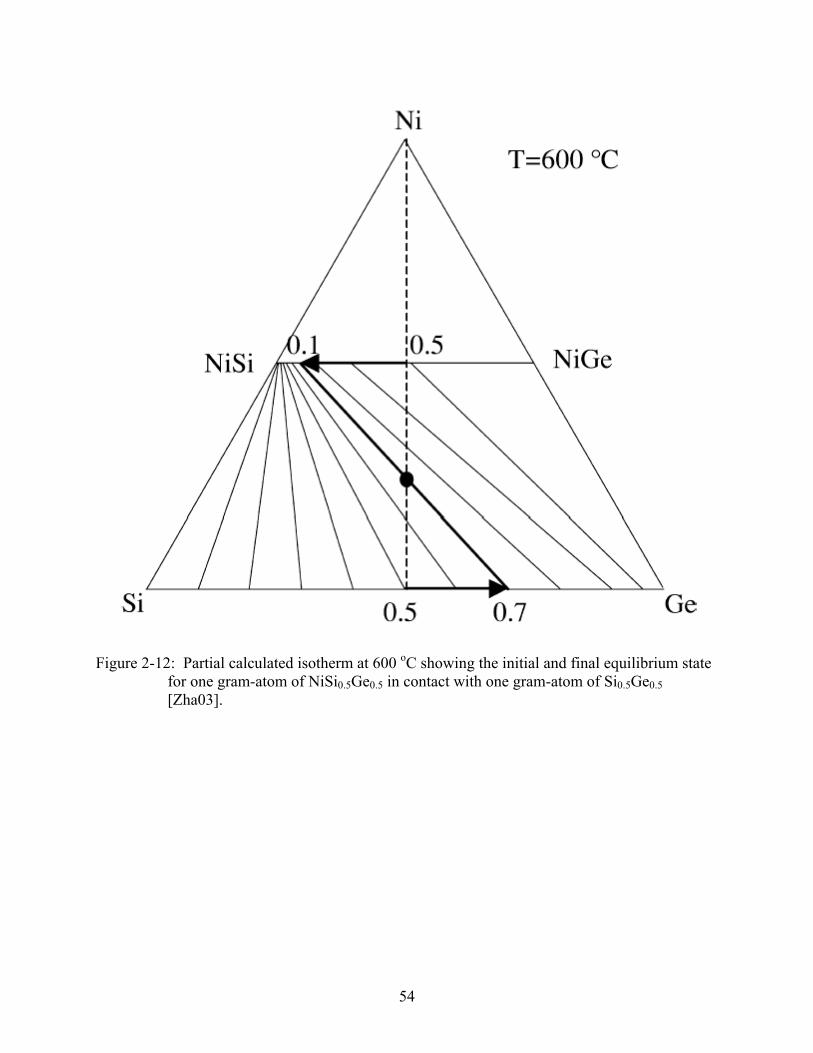
54
Figure 2-12: Partial calculated isotherm at 600 oC showing the initial and final equilibrium state for one gram-atom of NiSi0.5Ge0.5 in contact with one gram-atom of Si0.5Ge0.5 [Zha03].
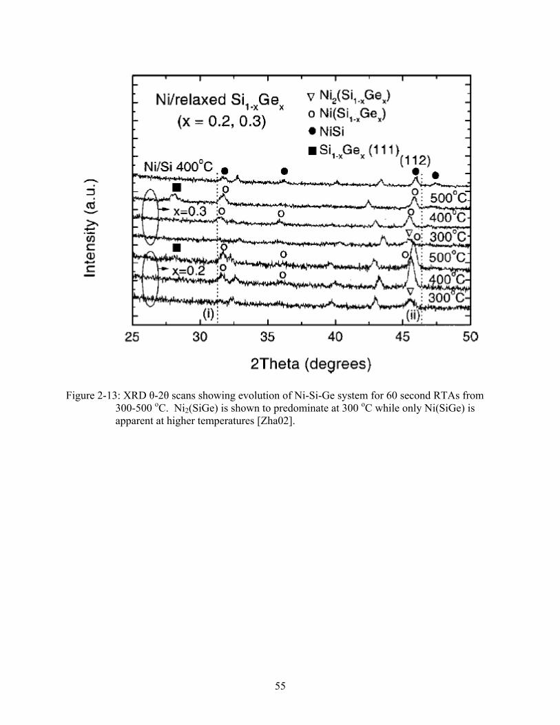
55
Figure 2-13: XRD -2 scans showing evolution of Ni-Si-Ge system for 60 second RTAs from 300-500 oC. Ni2(SiGe) is shown to predominate at 300 oC while only Ni(SiGe) is apparent at higher temperatures [Zha02].
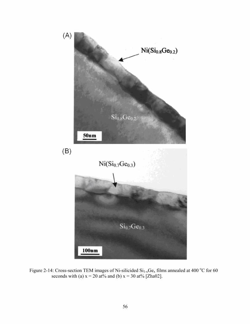
56
Figure 2-14: Cross-section TEM images of Ni-silicided Si1-xGex films annealed at 400 oC for 60 seconds with (a) x = 20 at% and (b) x = 30 at% [Zha02].
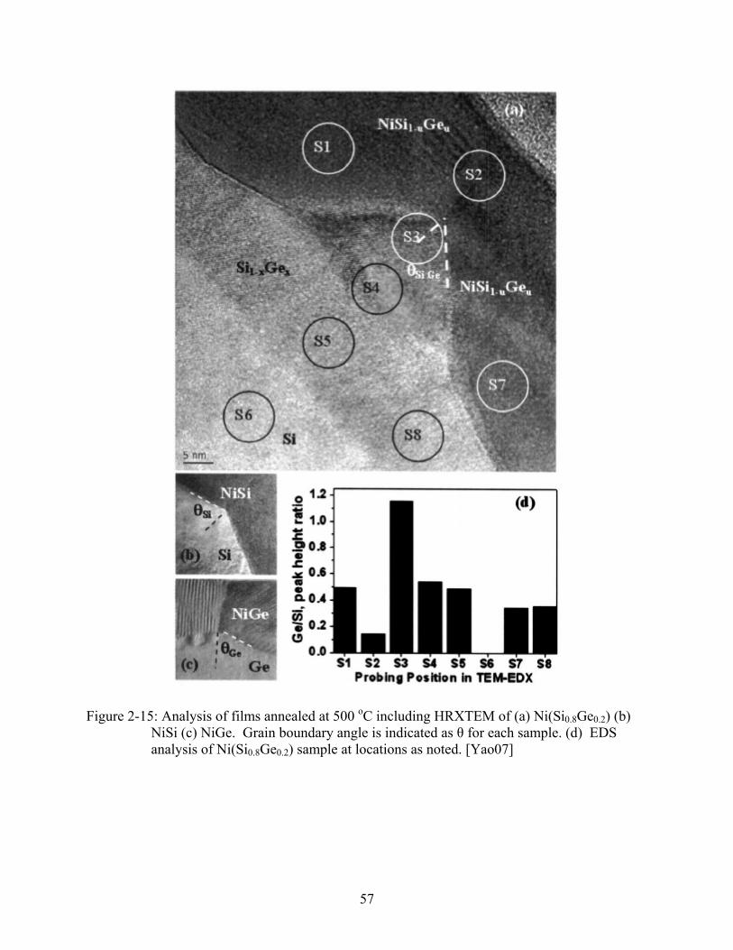
57
Figure 2-15: Analysis of films annealed at 500 oC including HRXTEM of (a) Ni(Si0.8Ge0.2) (b) NiSi (c) NiGe. Grain boundary angle is indicated as for each sample. (d) EDS analysis of Ni(Si0.8Ge0.2) sample at locations as noted. [Yao07]
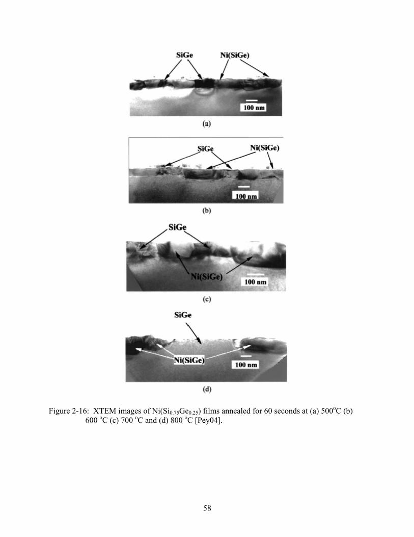
58
Figure 2-16: XTEM images of Ni(Si0.75Ge0.25) films annealed for 60 seconds at (a) 500oC (b) 600 oC (c) 700 oC and (d) 800 oC [Pey04].

59
Figure 2-17: Plan-view SEM analysis of Ni(Si0.9Ge0.1) grains annealed for 30 seconds at temperatures ranging from 650 to 750 oC [Ok03].

60
Figure 2-18: AES maps of Ge, Ni, and Si for Ni(Si0.75Ge0.25) samples annealed at 500, 700, and 900 oC for 60 seconds [Pey02].
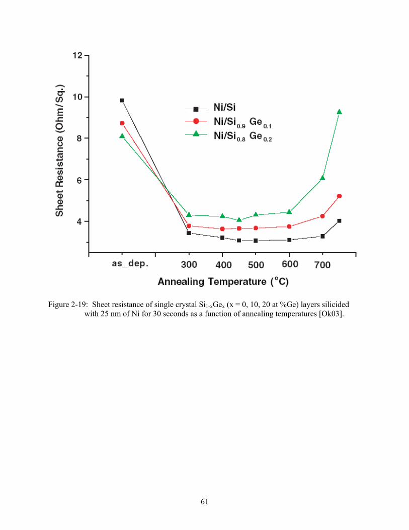
61
Figure 2-19: Sheet resistance of single crystal Si1-xGex (x = 0, 10, 20 at %Ge) layers silicided with 25 nm of Ni for 30 seconds as a function of annealing temperatures [Ok03].
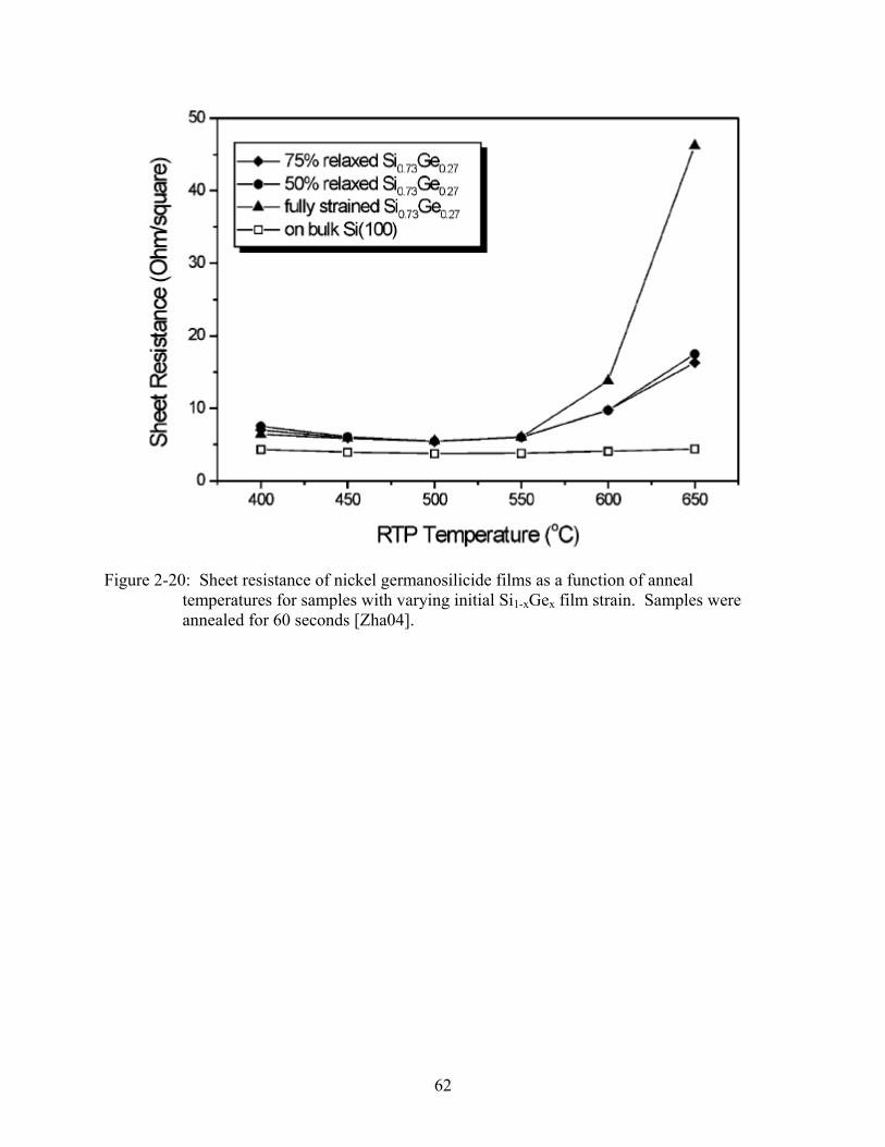
62
Figure 2-20: Sheet resistance of nickel germanosilicide films as a function of anneal temperatures for samples with varying initial Si1-xGex film strain. Samples were annealed for 60 seconds [Zha04].

63
Figure 2-21: Plan-view SEM images of nickel germanosilicide samples with varying concentrations of Ge (10 and 20 at%) in the initial Si1-xGex layer annealed at 650, 700 and 750 oC for 60 seconds [Ok03].
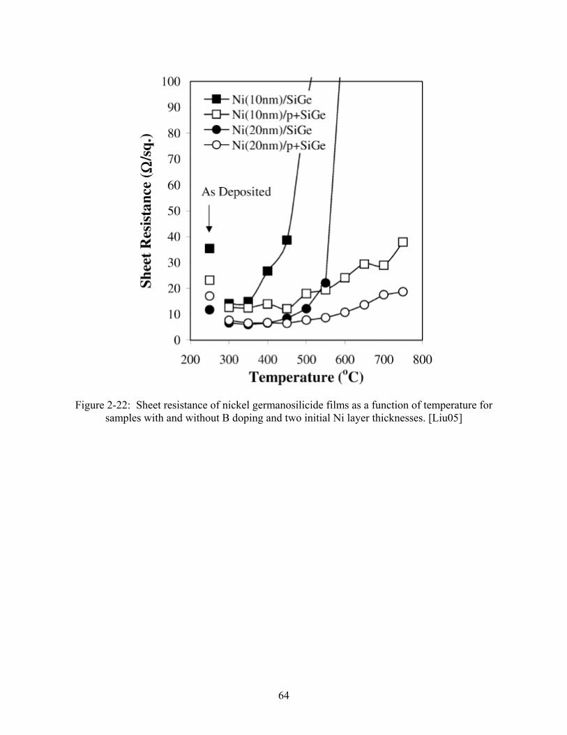
64
Figure 2-22: Sheet resistance of nickel germanosilicide films as a function of temperature for samples with and without B doping and two initial Ni layer thicknesses. [Liu05]

65
Figure 2-23: Plan-view SEM images of nickel germanosilicide films on As and B implanted single-crystal Si1-xGex. Samples underwent a two-stage anneal at 400 oC for 60 seconds and 450, 600, or 700 oC for 30 seconds.
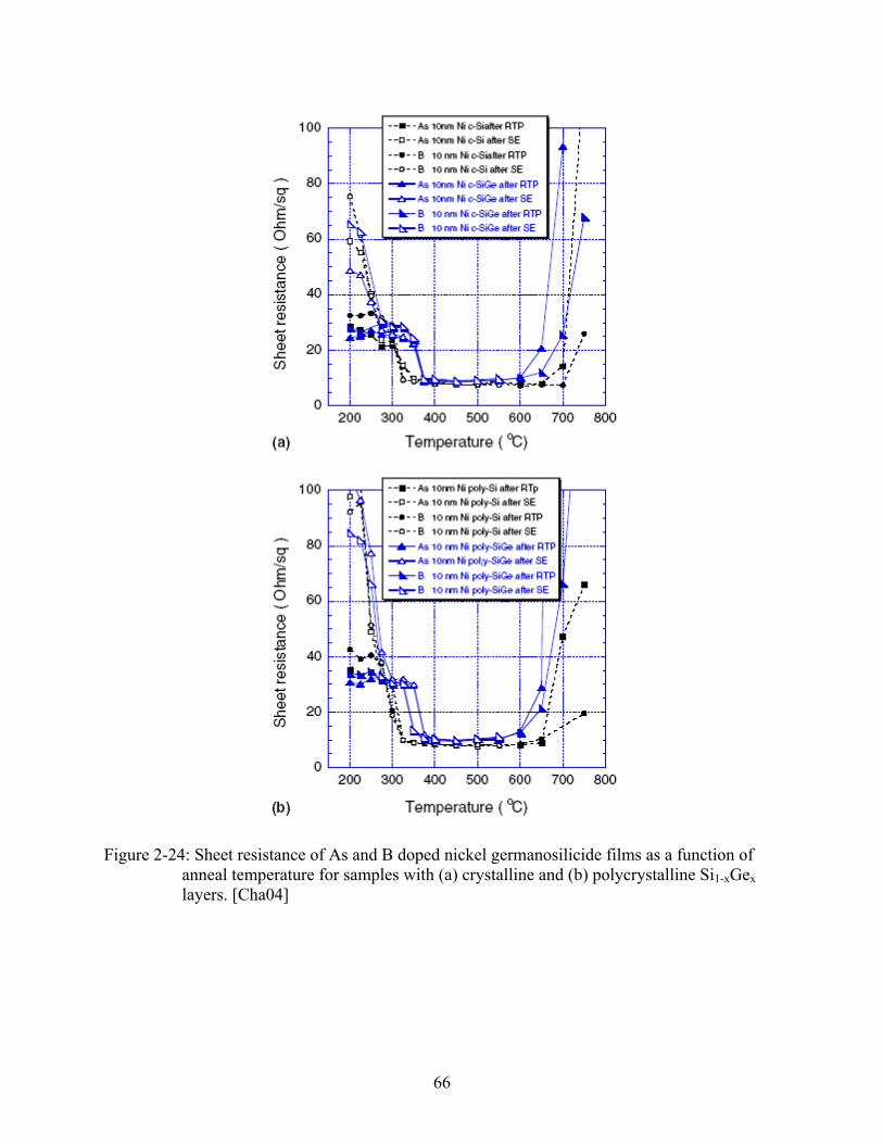
66
Figure 2-24: Sheet resistance of As and B doped nickel germanosilicide films as a function of anneal temperature for samples with (a) crystalline and (b) polycrystalline Si1-xGex layers. [Cha04]

67
Table 2-1: Measurement of average Ni(Si1-xGex)/Si1-xGex interface roughness for undoped and B-doped samples calculated via AFM after annealing at 400 and 500 oC for 30 seconds. [Liu05]
AFM Roughness Temperature Undoped Doped 400 oC 12.0 nm 4.4 nm 500 oC 18.0 nm 5.0 nm

68
CHAPTER 3 DESIGN OF EXPERIMENTS
3.1 Research Objectives
The objective of this work is to clarify certain outstanding issues regarding the
morphological stability and electronic properties of nickel germanosilicide thin films.
Specifically, this work aims to clarify the relationship between the rejection of Ge from the
initial film which results in the formation of Ge-rich Si1-zGez grains (commonly referred to as
film agglomeration) and observed increases in the sheet resistance of the film. While prior
works have proposed a qualitative link between the two properties, no quantitative relationship
has been put forth.
This work also aims to confirm whether the addition of high levels of B doping can
suppress the agglomeration process as suggested by Liu and Ozturk [Liu05]. Their work did not
utilize direct measurement techniques when evaluating film agglomeration and so the degree of
suppression, if any, is not well quantified. Regardless if suppression is confirmed to occur, this
work also aims to determine if the quantitative relationship between agglomeration and sheet
resistance is maintained for B doped samples.
Finally, prior studies available in literature utilize isochronal experiments with very short
annealing times. This work aims to expand the knowledge base of the behavior of nickel
germanosilicide films over a much larger range of anneal times and temperatures, including both
isochronal and isothermal series. By increasing the thermal matrix, information regarding the
kinetics of the phase transformation may be obtained.
Achieving these research objectives will lead to greater understanding of the stability and
properties of nickel germanosilicide thin films. This understanding, in turn, can be used to
further evaluate the use of the layers as intermediate contacts in semiconductor devices.
69
3.2 Factors and Levels
The choice of factors and levels used in this work were strictly constrained due to the lack
of availability of in-house wafer processing capability. Many factors known to affect the
behavior of nickel germanosilicide films, such as initial nickel layer thickness or Si1-xGex crystal
quality, require separate wafers to study each level. Thus, only the two such factors thought to
be most important were selected for this work: Ge concentration of the initial Si1-xGex layer and
homogeneous boron doping of the Si1-xGex layer during growth. As each of these factors was
varied at two levels, only four wafers were needed for all experiments performed in this work.
The other factors studied in this work, anneal temperature and anneal time, were able to be
varied over many levels as ample thermal processing ability was available.
It would have been possible to include other factors in the study with a relatively small
number of additional wafers through use of an experimental design allowing the screening of
multiple factors, such as a fractional factorial design. Such a design, however, was rejected as
the intent of this work was not to determine which factors are critical to nickel germanosilicide
growth (this knowledge is available in the literature) but to explore a few known factors in
greater depth.
3.2.1 Factors Altered
Four factors were varied in the experiment: anneal temperature, anneal time, Ge content in
the Si1-xGex film, and boron doping of the Si1-xGex film. The factors were varied over a range of
levels dependent upon the availability of resources. For temperature, levels of 450 to 800 ºC in
increments of 50 ºC were used. All thermal anneals were performed in a quartz-tube furnace
under a N2 ambient atmosphere. For time, levels of 10, 30, 90, 270, and 1020 minutes were
chosen. Anneal lengths were timed using a laboratory timer. For Ge content, levels of 15 and 25
at% were used. Higher Ge concentrations were not available due to limitations in reactor

70
processing capability. It is known that Ge composition is a critical factor in nickel
germanosilicide behavior as increasing Ge content will increase the thermodynamic driving force
for the rejection of Ge. This, in turn, results in increased reaction rates and the formation of Si1-
zGez grains with higher Ge content. It was expected that these differences would also affect the
sheet resistance of the films. The effect of increasing Ge concentration is also important since,
as previously discussed, it is expected that future device designs will utilize higher Ge
concentrations to increase the strain state of the device structures. For boron doping, levels of
undoped and homogeneously doped at a concentration of ~4.5E19 atoms/cm2 were selected.
While this concentration was lower than the ~1E21 atoms/cm2 used by Liu and Ozturk [Liu95],
it represents the maximum level possible with the reactor used to grow the material.
Homogeneous boron doping during growth is an important factor as it is likely to be included in
future device generations since, as previously discussed, it eliminates the need for implantation
and activation of source/drain well dopants.
All possible combinations of the factors and levels were performed and analyzed in this
work, resulting in each of the four experimental structures being studied over a significant
thermal matrix. Thus, the overall matrix may also be treated as either five isochronal or eight
isothermal anneal series. Analysis of the repeatability of the anneal process was also verified;
the results of this analysis is available in Appendix A.
3.2.2 Factors Held Constant
Additional factors determined by prior research to affect nickel germanosilicide formation,
stability, and electronic properties were not varied in this work. The factors held constant
include the initial Ni layer thickness and the crystalline quality, strain state, and thickness of the
Si1-xGex layer. While these factors are known to affect nickel germanosilicide film stability, they
71
are expected to be either less influential than those varied in this work, less likely to be varied in
future device designs, or both.
3.3 Experimental Structure
The relaxed Si1-xGex layers used in this work were grown using an ASM Epsilon 3200 RP-
CVD tool at Texas Instruments, Inc. Prior to deposition, (001) Si substrate wafers underwent a
HF clean and H2 bake at 1050 oC for 3 minutes to remove both the native Si oxide and any
contaminants from the wafer surface. Once cleaned, single crystal Si1-xGex layers were grown
using dichlorosilane and germane precursors in a hydrogen carrier gas with a flow of 40 standard
liters per minute. Borane was also included during growth for the boron doped samples. Growth
was carried out at 700 oC and a fixed pressure of 10 Torr. Final Si1xGex layer thickness was 150
nm. Subsequent to Si1-xGex layer growth, all wafers were capped with 10 nm of sputtered Ni
metal and 10 nm of TiN. It should be noted that the initial structure design called for only 0.5
nm of TiN deposition. As will be discussed in later chapters, however, the presence of the
excess TiN was not found to affect the behavior of the nickel germanosilicide nor did it impact
the analytical techniques utilized in this work.
3.4 Characterization Techniques
Several types of characterization techniques have been used to analyze the nickel
germanosilicide films studied in this work. These techniques include Cross-Section
Transmission Electron Microscopy (XTEM), Scanning Electron Microscopy (SEM), Electron
Dispersive Spectroscopy (EDS), Secondary Ion Mass Spectrometry (SIMS), Four Point Probe
(4PP), and the ImageJ image analysis software. It is important that the abilities and limitations
of each technique are understood so that the results they provide may be correctly interpreted.
Therefore, the following sections briefly describe each technique, how it may be applied to film
analysis, and information about the specific tools and methods used in this work. More in-depth
72
discussions of major techniques�’ fundamentals are available in other works, such as the text by
Brundle, Evans, and Wilson [Bru92].
3.4.1 Cross-Section Transmission Electron Microscopy
Transmission Electron Microscopy (TEM) is a technique which can be used to obtain
images, diffraction patterns, and composition information from a sample. To image a sample
with TEM, a beam of monochromatic electrons is focused on a very thin sample (typically less
than 200 nm thick). As the beam of electrons passes through the sample, some electrons are
inelastically scattered due to electron-atom interactions. Heavier atoms cause a stronger
interaction, which leads to increased scattering. The transmitted electrons may then be imaged
using a phosphorus screen or digital camera placed opposite and normal to the beam direction to
provide precise images of the sample with very high magnification. The differently scattered
electrons produce phase contrast in the image (areas of higher mass in the sample appear darker).
Electron-atom interactions can also produce x-rays characteristic of the scattering atom.
Characteristic x-rays may be captured by a dedicated detector and analyzed separately, a process
which will be discussed in a later section. This technique, called Energy Dispersive X-Ray
Spectroscopy (EDS), provides information about the atoms present in the analyzed region.
For analysis of nickel germanosilicide films, XTEM imaging is especially useful for
determining the thickness of the film as layers are directly measured (as opposed to calculated or
simulated from models with fitting parameters). The technique can also provide limited
information about the morphology of the film, such as the size and distribution of grains in the
layer, though it is important to consider that estimating these characteristics from cross-section is
much less preferred than using a plan-view analysis technique. When combined with EDS
analysis, the composition of the sample within a region of the image defined by the spot size of
the beam can also be semi-quantitatively determined.

73
In this work, two TEMs located at the Major Analytical Instrumentation Center (MAIC) at
the University of Florida were utilized for sample analysis. For low-magnification images, a
JEOL 200CX was used. For high resolution images, a JEOL 2010F was used. XTEM samples
in this work were produced using a FEI DB 235 Focused Ion Beam (FIB) mill to shape
membranes approximately 8 microns long, 5 microns tall, and 150 nm thick from the parent
material. The membrane was oriented such that its major plane was perpendicular to the surface
of the material and oriented such that the [110] direction was normal to the sample plane. Once
milled and fully cut away from the parent sample, XTEM samples were extracted using an ex-
situ micromanipulator and placed on 3mm nickel grids backed with carbon films for imaging in
the TEM. The XTEM samples were imaged in bright field along the <110> axis and/or in bright
field using a two beam condition with <220> g vector.
3.4.2 Scanning Electron Microscopy
Scanning Electron Microscopy (SEM) is a versatile technique which can provide a variety
of information about a sample. In SEM, a beam of energetic electrons is rastered (scanned)
across the surface of a sample. The electrons interact with the sample and produce secondary
electrons (SE), backscattered electrons (BSE), and characteristic x-rays; the signal associated
with each of the interactions can then be captured with an appropriate detector. Secondary
electrons, produced when primary electrons are inelastically scattered by atoms in the sample,
provide topographical imaging of the surface of the sample. Depressed areas, such as pits and
crevices, trap SE while raised areas, such as ridges and bumps, release more SE causing the areas
to be darker and brighter, respectively, in the image. Backscattered electrons, produced when
primary electrons are elastically scattered by atoms in the sample, provide images showing phase
contrast in the sample. The phase contrast occurs due to the higher likelihood of electrons being
elastically scattered by atoms with higher atomic numbers. Thus, regions with more massive
74
atoms will appear brighter in the BSE image. Finally, as in TEM analysis, characteristic x-rays
can also be produced when the primary beam interacts with the sample. The EDS analysis of
these x-rays is identical to that of those produced in TEM analysis and will be discussed in the
next section.
Both SE and BSE imaging modes can be used to analyze nickel germanosilicide films.
Plan-view SE imaging of the film surface and interfaces revealed by etching can provide
information about qualitative surface roughness. Plan-view BSE imaging of the films is
especially useful for monitoring the stability and size of the grains in the film as any non-uniform
changes in composition difference can create contrast in the image. Plan-view measurement of
grain size in either imaging mode also can provide direct measurements of grain size and
distribution over a relatively large sampling area defined by the magnification of the image. As
with TEM, when combined with EDS analysis the composition of the sample within a region of
the image defined by the spot size of the beam can also be semi-quantitatively determined.
In this work, a JEOL 6335F field emission SEM located at MAIC was used to image
samples. Plan-view samples for SEM analysis were prepared by cleaving small regions from
thermally processes wafer pieces. The small regions were then mounted to an aluminum SEM
puck using double sided carbon dots. The puck and samples were then coated with ~10 nm of
carbon to prevent charging of the sample during imaging. Samples were imaged at 9.63E-5 Torr
in BSE mode with a working distance of 9 mm, a probe current of 12 µA, and accelerating
voltage of 15 kV. Three images of each sample for quantitative analysis were taken at a
magnification of 30,000x and a scan speed of 23 seconds/frame. Image processing and
quantification is discussed in a later section of this chapter. While the reproducibility of the
imaging quantification process was unable to be studied due to limitations in personnel time and
75
availability, an analysis of the repeatability of the SEM imaging method used in this work is
presented in Appendix A.
3.4.3 Electron Dispersive Spectroscopy
As mentioned previously in the sections discussing TEM and SEM techniques, when a
high energy primary electron interacts with an atom a characteristic x-ray can be produced. In
this process, the primary electron causes the removal of an inner shell electron from the atom.
To compensate for the loss, an electron in a higher energy shell in the atom fills the inner vacant
position and after releasing its excess energy through the formation of an x-ray. The x-ray�’s
energy is characteristic of the atom as the difference between the two energy levels (inner and
outer) is, with few exceptions, different for each atomic species. If there are still higher energy
shells, the process will repeat until only the outermost shell is missing an electron. Thus, a single
strike may lead to the generation of a number of characteristic x-rays. The intensity of the x-rays
can then be detected and plotted as a function of their energy. From this graph, the atomic
species present in the sampled area can be identified and their relative concentrations semi-
quantitatively determined. It is important, however, to note that characteristic x-rays are also
produced throughout an interaction volume. Thus, depending on the spot size and energy of the
beam, signal may also be produced by adjacent regions such as neighboring grains or underlying
layers. These possible additional contributions must be considered when analyzing and
interpreting EDS results. It is also important to mention that EDS cannot provide absolute phase
identification (as can XRD analysis) since its results are semi-quantitative and lack any
information about the actual structure of the analyzed region.
For the study of nickel germanosilicide films, EDS offers a local analysis method capable
of determining the types and concentrations of atoms present within individual grains and, with
high-resolution tools, in proximity to grain boundaries and interfaces. These results, when used

76
in conjunction with SEM and/or TEM analysis, can provide greater insight into the imaged
structures in both cross-section and plan-view.
EDS analysis of XTEM samples in this work was performed using an Oxford Inca EDS
system on the JEOL2010F TEM located in the MAIC. A 1 nm nominal spot size was used for
point composition analysis, though a more accurate lateral resolution would be slightly higher as
both beam drift and beam spreading effects must be taken into consideration. Semiquantitative
analysis of the spectra was performed using the Cliff Lorimer thin ration section. The ratio of the
relevant atomic species (disregarding C, Cu signal from the TEM grid) was then determined to
arrive at an approximate local composition. It should be noted, however, that this process is very
approximate and significant error is likely present in the results. EDS analysis of plan view SEM
samples was performed using an Oxford Inca EDS system on the JEOL SEM 6400 located in the
MAIC. A nominal spot size of 5 nm was used for this analysis. The ratio method described
above was also used to determine approximate local composition for the plan view SEM
samples.
3.4.4 Secondary Ion Mass Spectroscopy
Compositional profiling of films is also possible using SIMS analysis; the technique is
especially appropriate for measuring smooth, continuous, multilayered structures. During SIMS
analysis, the sample is bombarded with a stream of ions which sputter particles, including
�“secondary�” ions, from the sample�’s surface. A mass spectrometer then measures the mass-to-
charge ratio of the secondary ions and this information is used to determine the average
elemental composition of the sputtered layer. As the sputtering process continues, more material
is removed and analysis moves deeper into the sample. In this manner, a raw SIMS profile of
ion intensity per unit time is obtained. The raw data may then be converted into a quantitative
composition profile as a function of depth by using a three step process. First, elemental signal

77
intensity is converted into elemental concentration based on variables including secondary ion
sputtering yield and detection efficiency. Next, sputtering time is converted into sputter depth
via calculations involving substrate sputtering rate. Finally, a depth resolution function (DRF)
must be assessed and used to reconstruct the original distribution of the atomic species.
Thus, SIMS analysis can be used to profile the composition of nickel germanosilicide films
as a function of depth. It is important to remember, however, that since SIMS analysis averages
the composition of each sputtered layer over the entire beam spot size a great deal of structural
information is lost during analysis (i.e. lateral composition differences). If an interface is rough,
SIMS analysis will also provide less-abrupt measurements of changes in concentration across the
interface. Use of SIMS analysis should therefore be confined to germanosilicide films that are
homogeneous and planar to provide optimal results.
SIMS analysis in this work was performed using a PHI Adept 1010 Dynamic SIMS
system located at the Advanced Materials Processing and Analysis Center (AMPAC) at the
University of Central Florida. Samples were analyzed using an 2 kV, 50 nA O2+ primary beam
and raw data was converted into concentration vs. depth plots using the sputtering rate and ion
yield of undoped or B-doped SiGe standards, as appropriate. Analysis was performed over a 300
µm square region with 10% detection area to avoid crater wall effects. It should be noted that
with these conditions, analysis of Ti and Ni containing layers will be less precise (especially for
thickness measurements).
3.4.5 Four Point Probe
Four point probe (4PP), also know as Kelvin probe, analysis can provide information about
the resistivity of a sample. In this technique, four terminals are placed in contact with a sample
along a straight line. The outer terminals and the sample form a circuit through which a set
current is passed. The inner terminals and the sample form a separate circuit which is passed
78
across a voltmeter. The voltmeter measures the decrease in potential between the two inner
probes and, with the knowledge of the sample geometry and applied current, can allow the
resistivity of the sample to be measured. Commonly, however, the resistivity of a thin film is not
reported. Instead, the sheet resistance of the film is often discussed. The sheet resistance of a
thin film is defined as the resistance measured for a thin film of equal length and width (a
square). Thus, sheet resistance is equal to the resistivity of the film divided be the film�’s
thickness and will be constant for any sized square sample. The sheet resistance of a sample can
be directly calculated from 4PP data and, with the use of geometrical correction factors, can also
be determined for an irregularly sized sample. It should be mentioned, however, that sheet
resistance alone cannot define all of the electronic properties of a film (i.e. contract resistance,
etc.) Nevertheless, sheet resistance does present a good general idea of the suitability of a film
as a current conductor.
Since the primary application of nickel germanosilicide films is to provide an intermediate
conduction layer between the souce/drain wells of a device and its interconnect metallization,
knowledge of a film�’s electronic properties is of great importance. Due to its relatively easy
measurement through use of 4PP analysis, sheet resistance is most often used to provide insight
into the electronic properties of a film. While other analysis techniques are sometimes applied to
determine additional electronic properties of the films, most of them require the formation of 2-
or 3-D test structures which adds to the expense and complexity of the analysis.
In this work, 4PP analysis was performed using rectangular wafer sections with nominal
measurements of 10 by 15 mm. Samples were analyzed using a Jandel Engineering multi height
probe with a linear configuration of carbide tungsten tips at a uniform spacing of 1.016 mm.
Samples were measured using a 900 µA current. If voltage readings could not be successfully

79
obtained with that level of current, the current was adjusted as necessary until successful
readings could be taken or the sample was determined to be non-conductive. Measurements
were performed at room temperature with the probe axis parallel to the long side of the wafer
sections in both forward and reverse current mode. A 10% difference in readings was allowed
between the forward and reverse modes; otherwise the probe location was adjusted until
measurements fell within the allowance. The average of both voltage (V) measurements was
then used in conjunction with the appropriate geometry correction factor (F) found in Table 3-1
and the probe current (I) to calculate the sheet resistance (Rs) of each sample according to Ohm�’s
law, given in equation 3-1.
FIVRs Equation 3-1
A gauge repeatability and reproducibility analysis of the 4PP analysis technique used in
this work is included in Appendix B. It was determined from this analysis that a 95% confidence
interval of +/- 2.19 Ohm/sq can be applied to each data point in order to capture any variation in
the measurement process.
3.4.6 Image Processing and Quantification
Quantification of SEM images is notably absent in prior work discussing nickel
germanosilicide thin films. Accordingly, a method of processing and quantifying images was
developed for this work. The majority of these tasks were performed using ImageJ v. 1.38x, a
public domain, Java-based image processing program developed at the National Institute of
Health. The program, available at the time of writing at http://rsb/info/nih.gov/ij/, contains a
large number of post-processing and image analysis options which may be used for a wide array
of purposes. In this work, ImageJ was first used to remove the area of the raw image containing
the scale bar in the SEM/BSE images by selecting the area of interest and using the �“crop�”
80
(Image>Crop) command. The noise in each images was also reduced though use of the
�“despeckle�” (Process>Noise>Despeckle) command and three applications of the
�“smooth�”(Process>Smooth) option. An example of a raw image is shown in Figure 3-1(a) and
the same image after processing is shown in Figure 3-1(b)
Once processed, a user-defined grayscale threshold was selected to differentiate between
contrasting grains, eliminating shades of gray and creating a binary image of black and white.
Selecting a threshold allows the area fraction and average size of the black or white areas in the
image to be quantified. Depending on the anneal conditions in this work, two or three phases
were visible in each image. Images with two phases present had a single threshold applied to
differentiate the phases. Images with three phases present had two thresholds individually
applied to distinguish either the lightest and darkest phase from the rest of the image. Examples
of thresholds applied to both types of images are shown in Figure 3-2.
The average grain size (in arbitrary units) and area fraction (in percent) of the black
regions was then calculated for each thresholded image using the �“analyze particles�”
(Analyze>Analyze Particles) tool. Final quantification values were determined for each sample
by averaging the results of three images taken of the same experimental sample. If present, the
area fraction of the third phase (the medium shade) was determined by subtracting the area
fractions of the other two phases from 100. Grain sizes of the third phase were not calculated for
reasons which will be discussed later. Error bars for the quantified results were statistically
determined to be +/- 3.35% for a 95% confidence interval; determination of this interval is
discussed in Appendix A.
For selected samples, the tortuosity of a connected phase was also calculated. Tortuosity,
in its simplest form, is defined as the measure of the twisting of a path. The most basic method

81
to calculate tortuosity ( ) is to divide the actual path length, L, by the minimum distance between
the endpoints of the path (its chord, C). This calculation is presented as Equation 3-2.
CL Equation 3-2
The quality of the SEM/BSE images in this work precluded the direct application of computer
software to determine tortuosity. Specifically, the images were too grainy and the contrast too
shallow for sufficiently accurate definition of individual grains and grain interfaces. Instead, the
tortuosity was roughly calculated by hand. First, a line of given length was randomly drawn on a
SEM/BSE image. The minimum length continuous path between the line endpoints within the
desired phase was then estimated and its length measured. The tortuosity was then calculated by
dividing the path length by the length of the initial line. An example of a SEM/BSE image with
the initial path as a blue dashed line and the estimated continuous path as a solid red line is
presented in Figure 3-3. This process was repeated three times for each image and the
measurements averaged to determine the tortuosity. The error in the tortuosity measurement will
be addressed in a later section.
3.4.7 Statistical Analysis
Statistical analysis of data was performed at many points in this work, including both
paired t-tests and ANOVA analyses. A paired t-test (also known as a dependant t-test) is a basic
statistical analysis technique which determines if the mean difference between two populations
from which paired observations are drawn is likely different from a reference value, usually zero.
For example, a paired t-test can be used to compare the grain size of samples with high and low
levels of Ge content at each point of a thermal matrix. Using a reference value of zero, the test
will determine whether it is statistically likely that changing Ge content affects grain size. By
82
pairing the samples, the test disregards the influence of anneal time and temperature and only
calculates the influence of the Ge concentration factor.
To perform a t-test, a t-statistic is calculated from the data by first determining the
difference (D = X2-X1) between each pair of samples according to Equation 3-3. Next, a t-
statistic is calculated from the values for D and the total number of paired samples (n) according
to Equation 3-4.
D = X2-X1 Equation 3-3
1)( 22
nDDn
Dt Equation 3-4
Once the t-statistic has been calculated, it is compared to a critical t-statistic found using the
desired confidence level and degrees of freedom (equal to n-1) from a standard t-distribution
table to determine if a statistically significant difference exists. Alternatively, a p-value may be
calculated from the t-statistic and, with the desired confidence level, used to evaluate the data. To
aid analysis, Minitab version 15.1.1.0 was used to perform the statistical calculations presented
in this work
Analysis of Variance (ANOVA) analyses are also used in this work as they offer the ability
to test whether there is a statistically significant difference between the levels of one or more
factors in a single analysis. The analysis can also determine if multiple factors combine to create
interactions (synergistic effects) in the response variable. Performing the calculations to
determine p-values for the factor and interaction terms in an ANOVA analysis, however, is a
complicated topic and the reader is referred to an introductory statistics text for a detailed
discussion of the theory and methodology of the analyses. As with the paired t-tests, Minitab
version 15.1.1.0 was used to the statistical calculations for the ANOVA analysis presented in this

83
work. Minitab analysis provides calculated p-values for each factor and interaction term and,
with the desired confidence level, these p-values may be used to determine the significance of
each factor.
3.5 Analysis of As-Grown Samples
Samples from the as-grown wafers used in this work were analyzed with XTEM to
ensure proper growth of the experimental structures. A representative XTEM image is shown in
Figure 3-4. Analysis of the images from the as-grown samples showed acceptable layer
thicknesses of 150 +/- 3 nm, 10 +/- 1nm, and 10 +/- 1 nm for the Si1-xGex, Ni, and TiN layers,
respectively. Interfaces in the as-grown samples were found to be smooth and abrupt. The
presence of dislocations at the Si1-xGex/Si interface was noted in all samples. While XRD
analysis of the Si1-xGex layer strain state was not performed on samples in this work, it is known
that the thickness of the Si1-xGex layer in each sample exceeds the critical value established for
strain relaxation [Mat74, Peo85]. It can be concluded, therefore, that the Si1-xGex layers in this
work are relaxed and any influence of strain on agglomeration will not be present in the samples.
SIMS analysis was also performed to confirm the Ge concentrations and B doping levels
of the as-grown wafers; the results from the analysis are presented in Table 3-2. Analysis of the
results indicates correct growth of the experimental structures. While the doped structure at the
lower Ge level showed a slightly lower Ge concentration than the undoped structure at the same
level, the difference is only ~2 at%. This difference is unlikely to cause significant variation in
the experimental results. The Ge distribution in the Si1-xGex layer was also found to be uniform
and continuous in the plots of concentration vs. depth, not included here. Analysis of the B
doped samples showed homogeneous, uniform doping levels of 4.58E19 and 4.33E19 atoms/cm3
for the low and high Ge level samples, respectively. This doping level represents the maximum
possible doping using the available reactors and processing time. With the XTEM results, these

84
findings allow the conclusion that the experimental structures used in this work were correctly
grown and may be directly compared.
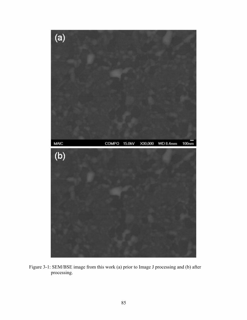
85
Figure 3-1: SEM/BSE image from this work (a) prior to Image J processing and (b) after processing.
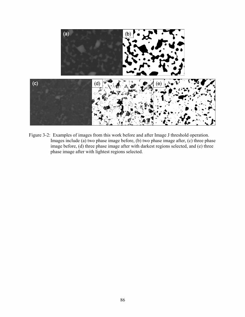
86
Figure 3-2: Examples of images from this work before and after Image J threshold operation. Images include (a) two phase image before, (b) two phase image after, (c) three phase image before, (d) three phase image after with darkest regions selected, and (e) three phase image after with lightest regions selected.

87
(a)
(b)
Figure 3-3: Example tortuosity measurement showing (a) raw SEM/BSE image of the undoped 25% Ge sample annealed at 450 oC for 1020 minutes and (b) the image after application of a Si1-zGez threshold by ImageJ and with a randomly placed line (blue dashed line) and the estimated minimum continuous path around the phase (red solid lines).

88
Figure 3-4: XTEM image of sample from as-grown wafer with x = 25 at% Ge and no B doping.
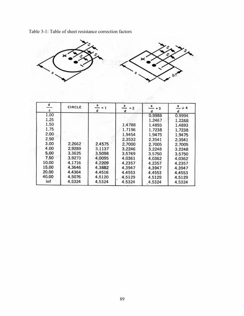
89
Table 3-1: Table of sheet resistance correction factors
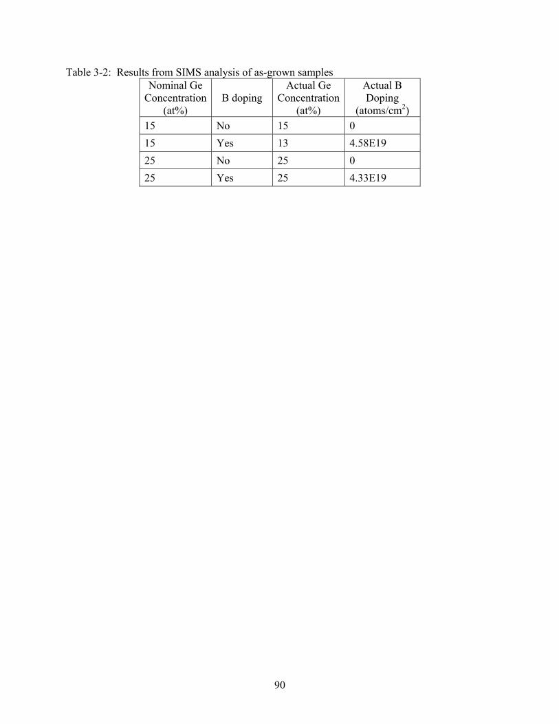
90
Table 3-2: Results from SIMS analysis of as-grown samples Nominal Ge
Concentration (at%)
B doping Actual Ge
Concentration (at%)
Actual B Doping
(atoms/cm2) 15 No 15 0 15 Yes 13 4.58E19 25 No 25 0 25 Yes 25 4.33E19
91
CHAPTER 4 INFLUENCE OF GE, B ON MICROSTRUCTURE AND KINETICS
This chapter explores the influence of both Ge content and the presence of homogeneous
in-situ B doping in the initial Si1-xGex layer on the microstructure and kinetics of nickel
germanosilicide thin films. It has been previously reported in literature that increasing Ge
content increases film sheet resistance by enhancing film agglomeration [Ok03, Zha04] and that
incorporation of high levels of in-situ doped B stabilizes sheet resistance by suppressing
agglomeration [Liu05]. None of these works, however, provide thorough microstructural
analysis, focusing mainly on cross section Transmission Electron Microscopy (XTEM) analysis.
XTEM analysis alone can provide good information concerning the depth distribution of phases.
Combined with EDS analysis, XTEM can also provide local phase composition and thus limited
information about the size and area fraction of phases present. While some works did apply
plan view Scanning Electron Microscopy (SEM), which provides good information about grain
size and phase area fraction, the technique was performed at relatively high magnification and
without quantification of the results. In the case of the work by Liu and Ozturk, direct
observation of the reported stabilization effect is not made at all; the presented conclusion was
based on sheet resistance measurements and roughness measurements of the nickel
germanosilicide/Si1-xGex interface. Without quantitative analysis, conclusive determination of
effects and relationships is not possible.
Prior work has also been generally confined to single isochronal rapid thermal anneals for
durations of 30 or 60 seconds. This limitation has prohibited the analysis of the reaction kinetics.
By annealing the samples in this work over a large thermal matrix of both time and temperature,
the kinetics of the nickel germanosilicide phase transformation from Ni(Si1-xGex) to Si-rich
Ni(Si1-uGeu) and Ge-rich Si1-zGez can also be investigated.
92
To accomplish these investigations, Ge content in the initial Si1-xGex layer was varied at
levels of 10 and 25 at% and the layers were either undoped or doped with ~4.5E19 atoms/cm3 of
B during growth. Microstructure analysis was performed on samples annealed in a quartz tube
furnace under N2 ambient at temperatures between 450 and 650 ºC in increments of 50 ºC for 10,
30, 90, 270, and 1020 minutes. Analysis included XTEM and SEM/BSE imaging as well as
limited application of EDS. Additional information on the experimental structure, processing,
and analysis methods was previously presented in Chapter 3. The follow sections discuss the
results from the analysis techniques to determine both the general microstructure evolution of the
samples as well as the kinetics of the transformation process, including both the reaction order
and activation energy.
4.1 Analysis using XTEM/EDS
As XTEM analysis provides limited information on film morphology, only selected
samples in this work were imaged using the technique. The analyzed samples were selected such
that they could be compared to prior work, ensuring that the films in this work behaved in a
consistent manner. Specifically, it was of interest to verify that at low anneal times and
temperatures the nickel germanosilicide film initially formed a homogeneous layer of Ni(Si1-
xGex) and then, at higher times and temperatures, this layer agglomerated into Si-rich Ni(Si1-
uGeu) and Ge-rich Si1-zGez grains. Accordingly, samples with 25% Ge content with and without
B doping were XTEM analyzed after anneals of 450 oC for 10 min and 550 oC for 10 and 1020
minutes. For better comparison to literature, which extensively uses 30 to 60 second RTA
anneals, samples with 25% Ge content with and without B doping were also RTA annealed for
60 seconds at 600 oC. Samples with 15% Ge content were not selected for analysis as it has been
previously shown that agglomeration increases with increasing Ge content [Ok03]. Thus, any
effect will be greatest, and most easily observed, in the 25% Ge samples.

93
Figure 4-1 presents an on-axis <110> XTEM images of 25% Ge undoped and doped
samples annealed at 450 oC for 10 minutes. It is apparent from the images that the films in this
work form a homogeneous nickel germanosilicide layer approximately 20 nm thick. These
results agree well with prior literature that reports the initial formation of a granular, continuous,
homogenous Ni(Si1-xGex) layer of uniform thickness [Zha02, Jon04, Ok04, Ko06, Yao07] prior
to the agglomeration process. It is also evident from the images that the presence of the
homogeneous B doping used in this work does not significantly affect film behavior at this time
and temperature, as the qualitative appearance of both images is identical.
On-axis <110> images of 25% Ge samples with and without B doping annealed at 550 oC
for 10 and 1020 minutes are shown in Figure 4-2. It is apparent from the phase contrast between
adjacent grains that the germanosilicide layers in the samples annealed at 550 oC for 10 minutes
have begun to transform into Si-rich Ni(Si1-xGex) and Ge-rich Si1-zGez grains. The
transformation is much more advanced, and evident, in the films annealed for 1020 minutes.
These samples show large, distinct grains of dark-contrast Si-rich Ni(Si1-xGex) interspaced with
thin grains of light contrast Ge-rich Si1-zGez (the relationship between grain contrast and
composition was confirmed by EDS, discussed later in this section). The features in these
images agree well with the intermediate and advanced stages of the phase transformation
previously reported in literature [Zha02, Pey02, Ok03, Pey04, Jin05]. As noted previously, the
addition of the homogeneous B doping in this work does not appear to affect the morphology of
the films in cross section.
For improved comparison to the XTEM/EDS results of prior literature, additional doped
and undoped 25% Ge samples were RTA annealed at 600 oC for 60 seconds. Figure 4-3 presents
the XTEM images of these samples taken at a tilt of 10o from the <110> zone axis (necessary for

94
EDS analysis on the TEM used in this work). As with the samples annealed at 550 oC for 1020
minutes, these images show a microstructure with large, distinct grains with dark contrast
interspersed between thin grains with lighter contrast. EDS analysis was performed on several
locations for both samples; the results are also shown in Figure 4-3. As previously mentioned,
the results indicated that the grains with dark contrast were Si-rich Ni(Si1-uGeu) and the regions
with light contrast were Ge-rich Si1-zGez. Additionally, the EDS analysis of the remaining Si1-
xGex layers agreed well with the SIMS analysis performed on the as-grown structures (22 and 23
vs. 25 and 25 at% for the undoped and doped samples, respectively). Overall, the EDS results
were found to agree well with previously reported germanosilicide film cross-section analyses
[Zha02, Pey02, Ok03, Pey04, Jin05]. It was also noted in the EDS analysis that the initial TiN
capping layer had oxidized to TiO2.
In summary, it can be concluded from the XTEM/EDS analyses presented in this section
that the evolution of the germanosilicide films in this work generally agrees with the progression
outlined in prior literature. Initially, at short annealing time and temperature, a homogeneous
layer of nickel germanosilicide forms. At higher times and temperatures, the homogeneous layer
transforms into grains of Si-rich Ni(Si1-uGeu) and Ge-rich Si1-zGez.
4.2 Plan View SEM Analysis
While XTEM analysis can provide valuable information about the cross section of a
sample, such as layer thicknesses, the technique is not well-suited to monitoring grain size or the
relative area fraction of phases present during a phase transformation. Hence, this work used
extensive plan view SEM analysis to monitor the microstructure of the nickel germanosilicide
films as they underwent the phase transformation from a homogeneous layer to an agglomerated
Si-rich Ni(Si1-uGeu) and Ge-rich Si1-zGez structure.
95
4.2.1 Phase Identification using EDS
As previously seen in the XTEM analysis, nickel germanosilicide films that are undergoing
a phase transformation from a homogeneous layer to an agglomerated structure show phase
contrast between the Si-rich Ni(Si1-uGeu) and Ge-rich Si1-zGez grains. Similar phase contrast was
also observed in plan view SEM images taken in both SE and BSE modes. An example of the
observed phase contrast is shown in Figure 4-4, where SE and BSE images of an undoped 25%
Ge sample annealed at 550 oC for 1020 minutes are shown. To identify the phases, an EDS line
scan of a undoped 25% Ge sample annealed at 550 oC for 1020 minutes was performed. The
results from this line scan, also presented in Figure 4-4, indicate that light contrast regions were
rich in Ni while the Si and Ge signal are relatively constant due to the influence of the underlying
Si1-xGex layer. These results indicate that the phase contrast seen in the SEM images was the
reverse of that seen in the XTEM images. The correct identification for the SEM results is that
light contrast regions correspond to Si-rich Ni(Si1-uGeu) grains and dark regions to Ge-rich Si1-
zGez grains.
4.2.2 Imaging and Phase Quantification using SEM/BSE
The microstructure of all samples annealed from 450 to 650 oC in 50 oC increments at
times of 10, 30, 90, 270, and 1020 minutes were plan view imaged in BSE mode according to the
method outlined in Chapter 3. As will be presented later, these samples capture the region of the
thermal matrix in which sheet resistance was decreased by the presence of B doping. It was of
interest, therefore, to determine if the B-doped samples in this region exhibited less
agglomeration according to the theory proposed by Liu and Ozturk [Liu05]. Additionally, as
will also be later discussed, this region of the thermal matrix also encompasses all successful
sheet resistance measurements of undoped samples. These samples were, therefore, of
96
maximum interest as their microstructure would allow a structure/property relationship to be
determined for both the doped and undoped samples (discussed in Chapter 5).
Figures 4-5, 4-6, and 4-7 present BSE images of the samples annealed for 10, 90 and
1020 minutes at temperatures of 450, 550, and 650 oC, respectively. In general, the samples all
show a similar morphological evolution with increasing time and temperature. At the lowest
times and temperatures used in this study, no contrast is evident in the images. This corresponds
to the homogenous initial film of Ni(Si1-xGex) previously seen in cross section in Figure 4-1(a)
and (b). As the time and temperature of the anneals increases, the images begin to show regions
of light and dark contrast which have been shown by Figure 4-4 to correspond to Si-rich Ni(Si1-
uGeu) and Ge-rich Si1-zGez grains, respectively. At yet higher times and temperatures, the
medium grey regions of Ni(Si1-xGex) disappear as the amount of Si-rich Ni(Si1-uGeu) and Ge-rich
Si1-zGez increases further. Finally, at the highest times and temperatures, the grains of Si-rich
Ni(Si1-uGeu) appear to begin to agglomerate. The evidence of agglomeration was further
investigated by imaging samples annealed at 750 oC for 10, 30, 90, 270, and 1020 minutes. The
BSE images of the samples annealed for 10, 90, and 1020 minutes are presented in Figure 4-8.
Distinct agglomeration is evident in these series of images; the samples annealed for 1020
minutes are qualitatively fewer in quantity and much more circular than those annealed at lower
times and temperatures. Therefore, it is expected that the agglomeration of the grains is resulting
in an increase in grain thickness. Support for this conclusion can be observed in the XTEM
images previously presented in Figure 4-2, where the Ni(Si1-uGeu) grains are much thicker in the
samples annealed for 1020 minutes than in the samples annealed for 10 minutes.
While prior studies of nickel germanosilicide films have relied on the qualitative analysis
of images, such as that leading to the previously discussed description of the evolution process,
97
this work makes extensive use of quantitative image analysis. As one of the main goals of this
work is to monitor the decomposition (usually referred to as agglomeration) of nickel
germanosilicide films, a quantitative metric linked to the process must be established. For this
work, that metric was selected to be the area fraction (or, occasionally, grain size) of the Ge-rich
Si1-zGez phase present in an image. As Ge-rich Si1-zGez is a product of the film transformation
process, the area fraction of this phase will increase with increasing agglomeration.
Accordingly, many of the analyses in this work will discuss the agglomeration process in terms
of the amount of Ge-rich Si1-zGez present.
4.2.2.1 Influence of Ge content
Prior works by Ok et al. [Ok03] and Zhang et al. [Zha04] have qualitatively established
that increasing the Ge content of the initial Si1-xGex layer increases nickel germanosilicide
agglomeration. The works, however, did not quantify the microstructures presented in their
results. While a qualitative comparison of the SEM/BSE images presented in Figures 4-5
through 4-8 of the samples with initial Si1-xGex layer concentrations of 15 and 25% Ge supports
their conclusions, the images in this work were also quantitatively analyzed.
Figure 4-9(a) and (b) plot a 95% confidence interval for the area fraction of Ge-rich Si1-
zGez as a function of annealing time for temperatures of 450, 550, and 650 for the undoped and
doped samples, respectively. Calculation of the area fraction range required for the 95%
confidence interval is presented in Appendix A. It should be noted, however, that while for
simplicity a single error range (established in Appendix A) was used for all values in these plots,
the actual error decreases with increasing area fraction. The quantitative results further support
the conclusion that increasing Ge content worsens film stability. At lower temperatures (450-
550 oC), the area fraction of precipitated Ge-rich Si1-zGez is much lower for the 15% vs. the 25%
Ge samples for both the undoped and doped structures. At higher temperatures, however, the
98
difference in Ge-rich Si1-zGez area fraction between the 15 and 25% Ge samples is much less.
This trend is also consistent in the quantitative analysis of the isothermal series not shown in the
figures (500, 600, 750 oC).
For further analysis, a paired t-test can be used to statistically compare the differences in
Ge-rich Si1-zGez area fraction at each point in the thermal matrix. A single paired t-test was
applied to all points on the thermal matrix for both the undoped and doped samples (i.e.
comparing the 15% Ge 500 oC 90 minute sample with the 25% Ge 500 oC 90 minute sample, and
also comparing the 15% Ge + B 500 oC 90 minute sample with the 25% Ge + B 500 oC 90
minute sample in the same statistical test). Accordingly, a total of 36 paired data points were
used in the analysis. The results from the analysis, presented in Figure 4-10, show that the
difference in Ge-rich Si1-zGez area fraction between the samples with 15 and 25% is statistically
significant at a 99.999% level (p=0.000), with the 15% Ge samples having a generally lower area
fraction (and hence less agglomeration). It is interesting, however, to note the range of the
difference in area fraction. The difference ranges from the 15% samples showing over 60%
(absolute) less area fraction to them having 3% (absolute) more. This range highlights the fact
that, while increasing Ge content definitively increases agglomeration at lower times and
temperatures, the effect is not consistent across the entire thermal matrix. The increase in
agglomeration is only present at lower times and temperatures. The cause of this discrepancy,
however, will be addressed in a later section.
4.2.2.2 Influence of B content
Previous work by Liu and Ozturk [Liu05] has suggested that the presence of high levels of
homogeneous B doping reduced nickel germanosilicide film agglomeration and led to the
stabilization of film sheet resistance. The previous work, however, lacked any direct observation
of the microstructure effect and instead formulated the theory from AFM measurement of the

99
germanosilicide/Si1-xGex interface and SIMS compositional depth profiles. A main objective of
this work was to determine, through direct, quantitative microstructure observation using plan
view SEM/BSE imaging, if this theory could be substantiated. While the homogeneous B
doping level in this work was limited by the ability of the reactor used to grow the experimental
structures, it will be presented in Chapter 4 that the B doped samples in this work exhibited a
similar decrease in sheet resistance when compared to undoped samples annealed at the same
time and temperature. Accordingly, a difference between sample microstructures for the doped
vs. undoped structures in this work was expected. The SEM/BSE images presented in Figures 4-
5 to 4-8, however, do not qualitatively support Liu and Ozturk�’s theory. The area fractions, grain
sizes, and interconnectivity of the phases present do not appear to differ between the undoped
and doped samples at any time or temperature for either the 15 or 25% Ge samples.
Quantitative analysis of the images provides further evidence that there is no difference in
area fraction or grain size between the undoped and doped samples in this work. Figure 4-11(a)
and (b) plot a 95% confidence interval for the area fraction of Ge-rich Si1-zGez as a function of
annealing time for temperatures of 450, 550, and 650 oC for the 15 and 25% Ge samples,
respectively. Calculation of the area fraction range required for the 95% confidence interval is
presented in Appendix A. It should be again noted that while for simplicity a single error range
was used for all values in these plots, the actual error decreases with increasing area fraction.
The plots for the undoped and doped samples appear to largely overlap within the experimental
error at all times and temperatures for both the 15 and 25% Ge samples. In fact, it appears if the
area fraction of Ge-rich Si1-zGez for the doped samples may be consistently slightly higher than
that of the undoped samples, suggesting that doped samples may display more agglomeration
than the equivalent undoped samples.

100
The validity of these conclusions may be further established by performing a paired t-test
to statistically compare the differences in Ge-rich Si1-zGez area fraction at each point in the
thermal matrix. Accordingly, a single paired t-test was applied to all SEM/BSE imaged points
on the thermal matrix for the 15 and 25% Ge samples (n = 36). The results from this analysis,
presented in Figure 4-12(a), show that there is no statistically significant difference in Ge-rich
Si1-zGez area fraction between the undoped and doped samples at a 95% confidence level.
While area fraction provides information on the quantity of a phase present in a
microstructure, the metric does not offer any information on the size or distribution of that phase.
A difference in grain size (with constant area fraction) could suggest that the interconnectivity of
grains may be altered with the addition of B doping. While this property appears qualitatively
identical in the SEM/BSE images of the undoped and doped samples presented in Figures 4-5 to
4-7, statistical analysis was also performed to determine if a quantitative difference existed.
Specifically, a single paired t-test as previously outlined for area fraction was used as the
statistical analysis method. The results from this analysis, presented in Figure 4-12(b), again
show that there is no statistically significant difference between the undoped and doped samples
at a 95% confidence level. Thus, in conjunction with qualitative observation of the images, it
can be concluded that the addition of B doping to the samples did not affect agglomeration,
either through an increase in the area fraction of the precipitated phase or by varying the grain
sizes of the precipitated (or any other) phase.
The quantitative results and statistical analysis in this work, therefore, strongly contradict
the conclusions drawn by Liu and Ozturk on the influence of homogeneous B doping in the
initial Si1-xGex layer. No statistically significant difference in either grain size or area fraction of
the Ge-rich Si1-zGez phase was determined at a 95% confidence level. While their results

101
indicate that the addition of B doping may decrease the roughness of the germanosilicide/Si1-
xGex interface, the decrease in roughness does not correlate to a decrease in agglomeration.
Instead, an alternate mechanism must lead to the reduction of sheet resistance in the B doped
samples observed in both works. This mechanism, and the structure/property relationship
between agglomeration and sheet resistance, is further addressed in Chapter 5.
4.3 Reaction Kinetics
The reaction kinetics of nickel germanosilicide agglomeration have not been established as
most published work has been confined to short, isochronal anneal series of 30 or 60 seconds.
Accordingly, without a full thermal matrix including anneals of multiple times and temperatures,
the reaction rate as a function of time and temperature cannot be calculated. This, in turn,
prevents the activation energy of the reaction to be established. Accordingly, this work utilized a
large thermal matrix incorporating a large range of times and temperatures in order to be able to
investigate the kinetics of the reaction process.
It should be noted that published literature (and, at times, this work) generally refers to the
�“agglomeration�” of nickel germanosilicide films. As shown in the SEM/BSE images in the
previous section, this term is somewhat of a misnomer. Agglomeration, according to the
Merriam-Webster dictionary, refers to �“the action or process of collecting in a mass�” [Mer04].
In materials science terminology, agglomeration is usually applied to a process in which a
precipitate, thin film, or other structure becomes more spherical in order to reduce the energy of
its interface. While XTEM micrographs of the nickel germanosilicide films in this work do
show some signs of spheroidization (and hence agglomeration in its strictest definition), it is well
established in both prior literature and this work that the film also rejects Ge and forms Ge-rich
grains of Si1-zGez. The process, therefore, was not and should not be treated as a pure
agglomeration process but instead be treated as (at least partially) a solid state transformation

102
reaction: the initial Ni(Si1-xGex) film transforms into Si-rich Ni(Si1-uGeu) and Ge-rich Si1-zGez
grains. Parallel or subsequent agglomeration of either phase may, in fact, need to be handled as a
separate event.
Transformation reactions have been widely studied across a variety of materials systems,
and a number of theories have been advanced to describe their kinetic processes. One kinetic
theory of transformation for a nucleation and growth process was proposed by M. Avrami
[Avr39, Avr40, Avr41] and well discussed in the text by J.W. Christian [Chr02]. This theory
considers the case where transformation begins at several points (nuclei) in a material. As the
transformed regions grow outwards from the nuclei, they eventually impinge on each other and
create a common interface over which growth ceases (though it will continue normally
elsewhere). Assuming an isotropic growth rate and a constant or decreasing nucleation rate per
unit volume, Avrami proposed a general relation for a three dimensional nucleation and growth
process. This relation, presented in Equation 4-1, relates the volume fraction transformed ( ) to a
rate constant (k), time (t), and the reaction order (n).
= 1 �– exp(-ktn) Equation 4-1
An extensive discussion of the theory behind the relationship is included in the text by Christian
[Chr02] and is beyond the scope of this work. It should be noted, however, that confining the
transformation within a 2-D film (and hence including the effects of a free surface) will modify
the reaction order by up to 1 (i.e. decrease n = 3 for a bulk system to n = 2 for a thin film).
Isothermal transformation curves of a process obeying the Avrami relationship will have a
sigmoidal shape on a linear plot of vs. t. It is difficult, however, to fit linearly plotted
sigmoidal data in order to determine n and k for a set of experimental results. Accordingly,

103
Equation 4-1 may be mathematically transformed to produce the relationship given by Equation
4-2.
log(log((1- )-1) = n(log(t)) + log(k) Equation 4-2
It can be seen from Equation 4.2 that a plot of log(log((1- )-1) vs. log(t) will produce a straight
lines with slope n and y-axis intercept of log(k) for an isothermal transformation curve of a
process that obeys the Avrami relationship. Thus, experimental data from a process thought to
obey Avrami kinetics is often graphed on such a plot and analyzed using linear regression
analysis after the appropriate transformations have been made.
The isothermal transformation curves in Figures 4-9 and 4-11 do not show a classic
sigmoidal shape as the curves are increasing in value from the earliest time. The lack of classic
shape, however, does not preclude the process obeying Avrami kinetics, however. Instead, it
illustrates that the initial nucleation period may be very short (i.e. the first part of the sigmoidal
shape may lie below 10 minutes). It was of interest, therefore, to determine if the nickel
germanosilicide transformation obeyed the Avrami theory. As the volume fraction of
transformed phase was not determined in this work, the area fraction of the phase was
substituted. This substitution is justified as the reaction can be generally assumed to be confined
in a thin layer (as shown by the XTEM in Figures 4-1 and 4-2). Plots of log(log((1-AF)-1) vs.
log(t) will still produce straight lines with slope n and y-axis intercept of log(k) for a process
obeying Avrami kinetics. As mentioned previously, however, the reaction order will be reduced
by up to 1.
4.3.1 Reaction Order
To determine n, the reaction order, the log(log((1-AF)-1) of all imaged sample conditions
were plotted as a function of log(t). The plots are presented in Figure 4-13 for the undoped and
doped 15% Ge samples and in Figure 4-14 for the undoped and doped 25% Ge samples. As it
104
was determined in the preceding discussion that, while Ge content influenced film
microstructure, homogeneous B doping did not, the undoped and doped samples were considered
and analyzed as a single case (though the provenance of each data point was maintained on the
graphs). Restated, while the undoped and doped samples are plotted separately on the graphs,
single statistical regressions containing all data points (both undoped and doped) was performed
for each combination of Ge composition and anneal temperature. It should also be noted that,
due to the mathematical transformation, the error bars plotted for the transformed log(log((1-
AF)-1) values are not constant, as shown, but actually vary with area fraction. A more
comprehensive explanation of this effect and the reasoning behind the selection of the displayed
error ranges is contained in Appendix C.
It is evident from Figures 4-13 and 4-14 that while most temperature series appear to be
linear, all anneal temperatures do not share a constant slope in either plot. Furthermore, the
results from the 600 oC anneal series for the 15% Ge samples and the 550 oC series for the 25%
Ge samples do not appear to be linear. An explanation for this effect can be determined by
analysis of a plot of the area fraction of the initial Ni(Si1-xGex) phase as a function of Ge-rich Si1-
zGez area fraction, presented in Figure 4-15. It is evident from this figure that for all samples,
regardless of Ge or B content, the initial Ni(Si1-xGex) phase disappears by ~60% Ge-rich Si1-zGez
area fraction. When transformed for the Avrami plots, the log(log((1-AF)-1) of 60% area fraction
corresponds to a value of -0.400. A horizontal line of this value plotted on the graphs shown in
Figures 4-13 and 4-14 would divide the graphs into two regions. Above and below this line, the
slopes of all temperature series appear to be qualitatively equal, including the corresponding
sections of the 550 and 600 oC plots. These results, along with the earlier observation of the film
105
morphology in plan view SEM/BSE, confirm that the nickel germanosilicide film evolution must
be considered as two separate reactions: precipitation and agglomeration.
4.3.1.1 Precipitation reaction
Figure 4-16(a) and (b) present the sections of the Avrami plots lying below 60% area
fraction Ge-rich Si1-zGez for the 15% and 25% samples, respectively. These regions of the plot
correspond to the precipitation stage of the transformation reaction, where the Ge-rich Si1-zGez
phase is being formed through Ge rejection from the initial Ni(Si1-xGex) phase and reaction with
the remaining Si1-xGex layer. Linear regression analysis for every temperature series appearing
in each plot was performed using the Minitab software; the results from the regression analysis
are presented in Table 4-1 and the best fit equation lines are plotted in Figure 4-16(a) and (b).
The average value of n for the 15% Ge samples was determined to be 0.676 +/- 0.142 for a 95%
confidence level. For the 25% Ge samples, n was determined to be 0.491 +/- 0.106 for the same
confidence level. With the previously mentioned influence of a 2-D film on n, it can be
concluded that the equivalent n for this reaction in a bulk material would be between ~0.5 and
1.5. This value for n can be compared to a table of values from the text of Christian [Chr02],
presented in Table 4-2, for diffusion controlled reactions obeying Avrami behavior. While
several types of growth have n values between 0.5 and 1.5, the only reaction which can describe
the morphology seen in Figures 4-5 to 4-7 is that of �“all shapes growing from small dimensions,
zero nucleation rate�” which has n = 1.5. It can be concluded, therefore, that the first stage of the
nickel germanosilicide transformation is of this type. This conclusion is further supported by the
prior work of Yao et al. [Yao07] who showed that Ge enrichment occurred at grooves formed
between neighboring germanosilicide grains (see Figure 2-15). These results, which suggest that
grain boundary nucleation is occurring, support the conclusion that a zero nucleation rate is in

106
effect, as no new grain boundaries are likely to be formed during the reaction in unreacted
regions.
4.3.1.2 Agglomeration reaction
Figure 4-17(a) and (b) present the sections of the Avrami plots lying above 60% area
fraction Ge-rich Si1-zGez for the 15% and 25% samples, respectively. These regions of the plot
correspond to the agglomeration stage of the transformation reaction, where the Ge-rich Si1-zGez
area fraction increases as the Si-rich Ni(Si1-xGex) phase agglomerates. Linear regression analysis
for every temperature series appearing in each plot was performed using the Minitab software;
the results from the regression analysis are presented in Table 4-3 and the best fit equation lines
are plotted in Figure 4-17(a) and (b). The average value of n for the 15% Ge samples was
determined to be 0.067 +/- 0.023 for a 95% confidence level. For the 25% Ge samples, n was
determined to be 0.056 +/- 0.015 for the same confidence level. With the previously mentioned
influence of a 2-D film on n, it can be concluded that the equivalent n for this reaction in a bulk
material would be between ~0.05 and 1.05. This value for n can be compared to the table of
values from the text of Christian [Chr02], formerly presented in Table 4-2, for diffusion
controlled reactions obeying Avrami behavior. The results of this comparison suggest that the
reaction is the diffusion controlled �“thickening of very large plates (e.g. after complete edge
impingement)�” which has a bulk n of 0.5. This conclusion is supported by the previously
presented XTEM (Figure 4-2) and SEM/BSE images (Figures 4-5 to 4-7) in this work and in
prior work (Figure 2-16) which show both the Ge-rich Si1-zGez and Si-rich Ni(Si1-xGex) to have
large, plate-like morphologies.
4.3.2 Activation Energy
The linear regression analyses necessary to determine the order of the reactions also
provided values for log(k). These values, reported in Tables 4-1 and 4-3 for the precipitation and
107
agglomeration reactions, respectively, may be mathematically converted to ln(k) and used to
determine the activation energy (Ea) of each reaction according to the Arrhenius equation, which
is presented as Equation 4-3:
ln(k) = -Ea (1/KT) + ln(A) Equation 4-3
From this equation, where K is Boltzmann�’s constant (8.67e-5 eV/K), it is apparent that on a plot
of ln(k) vs. (1/KT), Ea will be equal to the negative slope of the line. Figure 4-18(a) and (b)
present such plots for the precipitation and agglomeration reactions, respectively. While each
data point on these graphs has a unique error range (calculated from the standard error of log(k)
in Tables 4-1 and 4-3), the error for each reaction series was found to be relatively consistent.
Hence, for simplicity, a single error range corresponding to a 95% confidence interval for the
average standard error was presented for each series on the graphs in Figure 4-18. The error
ranges are equal to +/- 0.680, 0.459 for the 15 and 25% Ge precipitation reactions and +/- 0.117,
and 0.078 for the 15 and 25% Ge agglomeration reactions, respectively. Linear analyses were
performed on the reaction series shown in Figure 18; the results from the analyses are presented
in Table 4-4 and will be discussed in the following paragraphs.
4.3.2.1 Precipitation reaction
For the precipitation reaction, Figure 4-18(a) and the results in Table 4-4 show that the
activation energy for the 15% Ge samples was higher than for the 25% Ge samples. A two-
sample t-test using the appropriate data from Table 4-4 shows the nominal difference in
activation energy to be 1.196 eV, with a 95% confidence interval for the difference ranging
between 0.595 and 1.797 eV. While this analysis is formed using somewhat limited data (four
points for the 15% sample and three for the 25% sample), the difference is significant and the
error range for the data relatively small. It is unlikely, therefore, that additional data points
would cause enough of a shift in the linear regression to eliminate the difference in activation

108
energies. It can be concluded, accordingly, that a statistically significant difference in activation
energies for the precipitation reaction exists when Ge content is increased.
It is evident from these results that the activation energy of this reaction is concentration
dependant; increasing Ge content from 15 to 25% in the initial Si1-xGex layer decreased the
activation energy by ~1.2 eV. The precise cause of this decrease it not known. Many steps of
the reaction, however, have been found to be concentration dependant in other system. Such
steps include the bonding energy between atoms (which must be broken to switch from Ni-Ge to
Ni-Si), and the diffusion of atoms in an alloy. An example of a concentration influence on
bonding energy can be found in the work by J. Tersoff, where bond strength was calculated to
decrease with increasing Ge content in Si1-xGex [Ter89]. Experimental evidence of this effect has
also been reported [Cros03]. An example of concentration dependant diffusion activation energy
has been shown by Zangenburg et al., who studied the diffusion of Ge in Si1-xGex alloys [Zan01].
Their work showed that the activation energy of Ge diffusion in silicon germanium alloys
decreases with increasing Ge content. It can be extrapolated from their results that the activation
energy decreases from 4.33 to 3.92 eV for a change in composition from 15 to 25% Ge, a
difference of 0.42 eV.
It is likely, therefore, that the influence of Ge on activation energy could be accounted for
by similar concentration dependent effects, as the initial (metastable) Ni(Si1-xGex) films contain
different compositions of Ge based upon the concentration of the Si1-xGex layer being silicided.
Additional research into the bond strengths and mobility of Ni, Si, and Ge in nickel
germanosilicide films is needed, however, to determine if a single concentration dependant effect
dominates and creates the difference in activation energy, or if the difference is a compilation of
109
two or more lesser effects. The concentration dependency should also be studied over a greater
range of Ge compositions to determine the other composition ranges to establish a stronger trend.
4.3.2.2 Agglomeration reaction
Figure 4-18(b) and the results in Table 4-4 show approximately equal activation energies
for the 15 and 25% Ge samples undergoing the agglomeration reaction. A two-sample t-test
using the appropriate data from Table 4-4 shows the nominal difference in activation energy to
be 0.044 eV, with a 95% confidence interval for the difference ranging between -0.0054 and
0.0931 eV. It can be concluded, therefore, that no statistical difference between the reactions
exists at the 95% confidence level. While this analysis is formed using somewhat limited data
(three points for the 15% sample and four for the 25% sample), the nominal difference is small in
relation to the error of the data. It is unlikely, therefore, that additional data points would cause
enough of a shift in the linear regression to cause significant difference in the activation energies.
Thus, unlike for the precipitation reaction, this work found no statistically significant
difference in activation energy for the agglomeration reaction between the 15% and 25% Ge
samples. It can be concluded, therefore, that this reaction does not have a dependency on Ge
concentration. The lack of concentration dependence, however, is not unreasonable. The
agglomeration reaction does not result in any composition changes. Instead, it is likely driven
solely by the minimization of free energy through geometric rearrangement of the Ni(Si1-uGeu)
grains (i.e. minimizing surface area to volume ratio); a conclusion also supported by observation
of the generally circular shape of the Ni(Si1-uGeu) grains after annealing at high times and
temperatures. With consideration of the fact that the compositions of the Ni(Si1-uGeu) grains for
both the 15 and 25% Ge samples are very close (less than ~1 at%) at the completion of the
precipitation reaction (and hence the start of the agglomeration reaction), it is possible that the
rearrangement is occurring by a mechanism which occurs within the Ni(Si1-uGeu) grains. Thus,
110
the mechanism would not be influenced by the external variations in Ge concentration. As with
the precipitation reaction, however, not enough information about the Ni-Si-Ge system (mobility,
diffusivity) is known to draw a firm conclusion as to the exact nature of the mechanism beyond
the fact that it is not very temperature dependant as indicated by the small activation energy.
4.4 Summary
A number of important conclusions can be drawn from the work presented in this chapter.
First, the general cross-section and plan-view morphology of the nickel germanosilicide films in
this work agree well with those reported in prior literature. Second, while prior work has
generally described the film evolution as �“agglomeration,�” two distinct reactions have been
captured by the anneal matrix used in this work. Initially, Ge-rich Si1-zGez grains precipitate
from the parent film as Ge is rejected to the grain boundaries. This process continues until the
parent film has completely transformed in to Ge-rich Si1-zGez and Si-rich Ni(Si1-uGeu) grains.
Complete transformation corresponds to ~60% area fraction Ge-rich Si1-zGez for all samples in
this work. Once the transformation is complete, the Si-rich Ni(Si1-uGeu) grains begin to
agglomerate. Third, increasing Ge content in the initial Si1-xGex film from 15 to 25% increases
the amount of transformation observed for equivalent anneals, likely due to the increase in
activation energy for Ge rejection with increasing Ge content. Fourth, the addition of ~4.5E19
atoms/cm2 homogeneous B doping during Si1-xGex layer growth does not affect nickel
germanosilicide film microstructure for any anneal. Finally, Avrami reaction kinetics can be
used to model the isothermal transformation curves of nickel germanosilicide thin films. Two
separate reaction orders were observed, corresponding to the precipitation and agglomeration
reactions. By analysis of the reaction order, the precipitation reaction was determined to be
diffusion controlled growth with a zero nucleation rate. The agglomeration reaction was
similarly determined to be diffusion controlled thickening of very large plates. The activation
111
energies of the reactions were also able to be calculated and showed that for the precipitation
reaction, Ea was 1.96 and 0.76 eV for the 15 and 25% Ge samples, respectively. For the
agglomeration reaction, Ea was determined to be 0.14 and 0.10 eV, respectively (though
statistically these values were found to be equal).

112
Figure 4-1: On-axis <110> XTEM images of 25% Ge samples annealed at 450 oC for 10 minutes with (a) no doping and (b) B doping
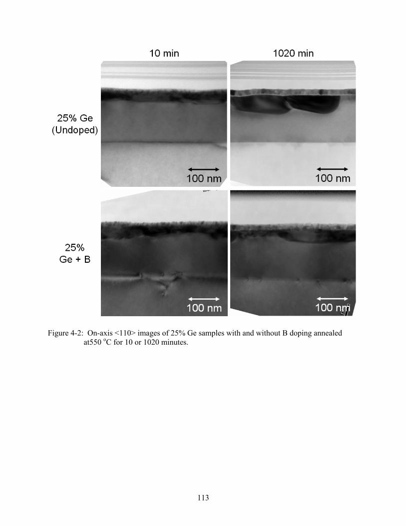
113
Figure 4-2: On-axis <110> images of 25% Ge samples with and without B doping annealed at550 oC for 10 or 1020 minutes.

114
Figure 4-3: XTEM images taken at 10o tilt from <110> zone axis of undoped and doped 25% Ge samples RTA annealed at 600 oC for 60 seconds. The locations and results of EDS analysis are indicated on the image.
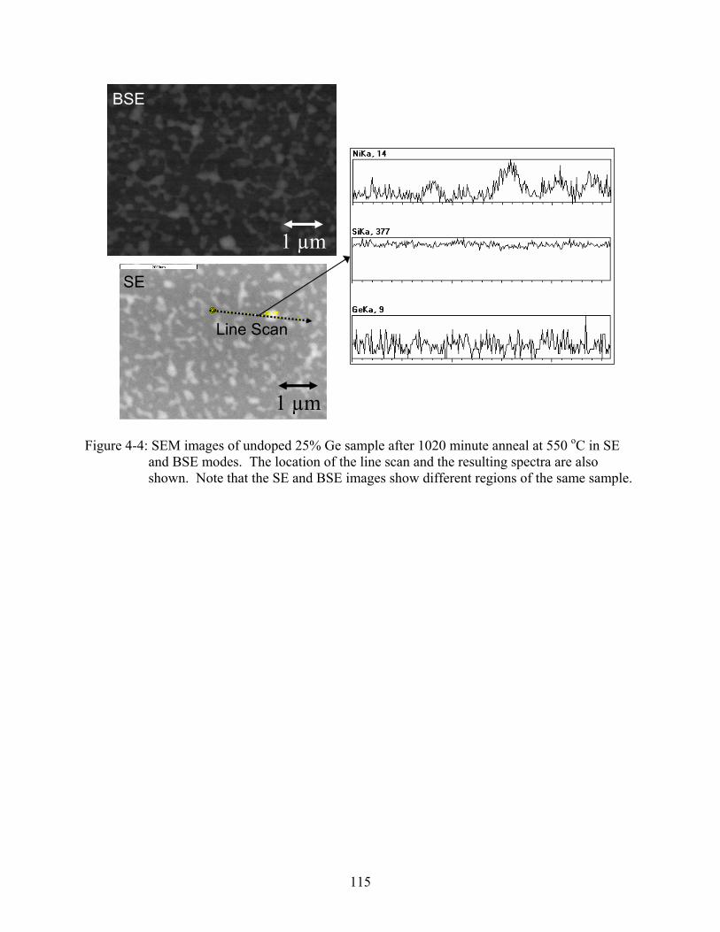
115
1 µm
1 µm
BSE
SE
Line Scan
Figure 4-4: SEM images of undoped 25% Ge sample after 1020 minute anneal at 550 oC in SE and BSE modes. The location of the line scan and the resulting spectra are also shown. Note that the SE and BSE images show different regions of the same sample.

116
Figure 4-5: SEM/BSE images of samples annealed at 450 oC
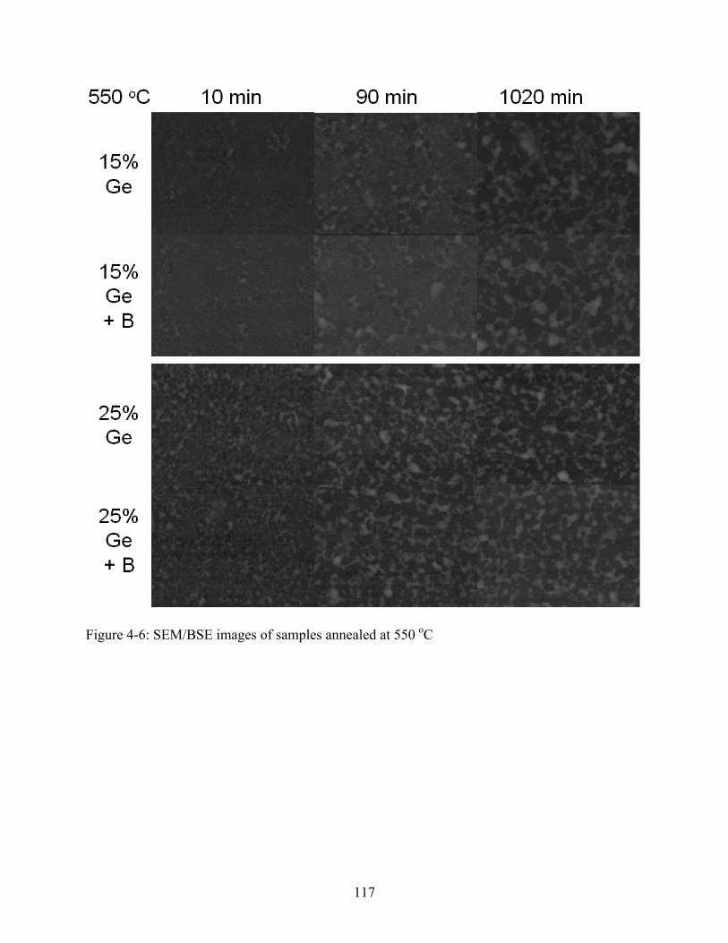
117
Figure 4-6: SEM/BSE images of samples annealed at 550 oC
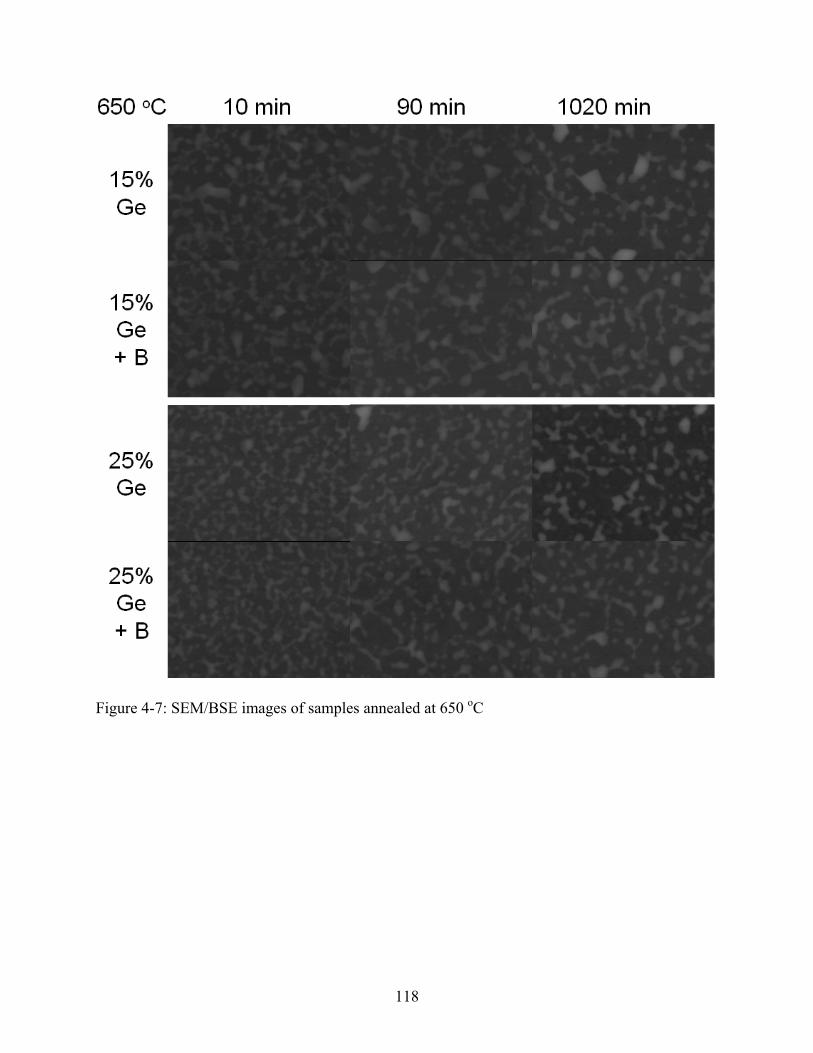
118
Figure 4-7: SEM/BSE images of samples annealed at 650 oC
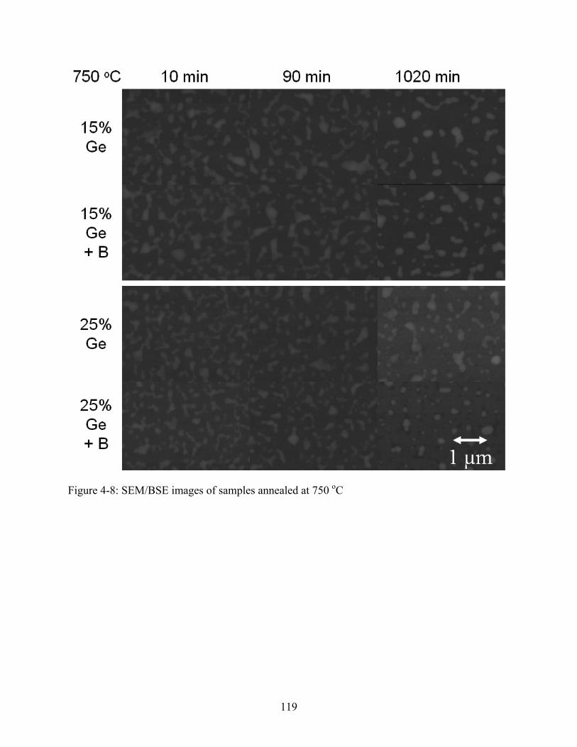
119
Figure 4-8: SEM/BSE images of samples annealed at 750 oC

120
Undoped
0
10
20
30
40
50
60
70
80
90
100
0 200 400 600 800 1000 1200time (min)
AF
Si(1
-z)G
e(z)
15% Ge, 450 C15% Ge, 550 C15% Ge, 650 C25% Ge, 450 C25% Ge, 550 C25% Ge, 650 C
Doped
0
10
20
30
40
50
60
70
80
90
100
0 200 400 600 800 1000 1200time (min)
AF
Si(1
-z)G
e(z)
15% Ge + B, 450 C15% Ge + B, 550 C15% Ge + B, 650 C25% Ge + B, 450 C25% Ge + B, 550 C25% Ge + B, 650 C
(a)
(b)
Figure 4-9: Area fraction of Ge-rich Si1-zGez phase as a function of anneal time at temperatures of 450, 500, and 650 oC for (a) undoped samples and (b) doped samples.
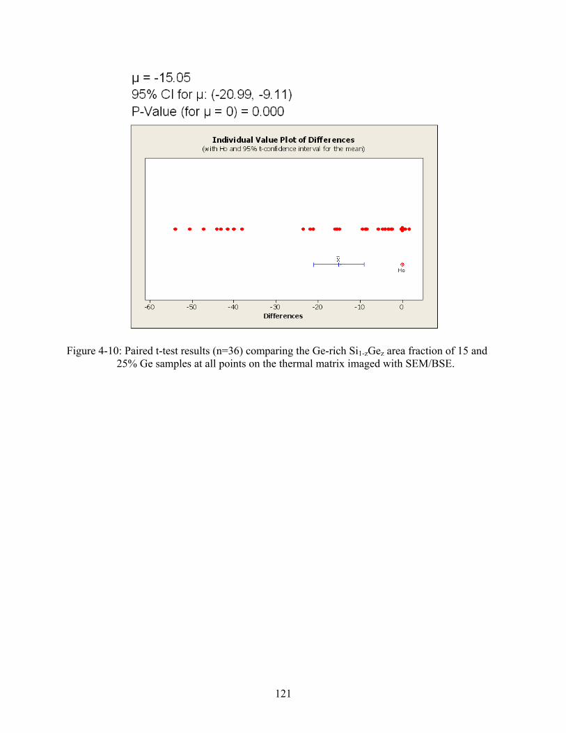
121
Figure 4-10: Paired t-test results (n=36) comparing the Ge-rich Si1-zGez area fraction of 15 and 25% Ge samples at all points on the thermal matrix imaged with SEM/BSE.
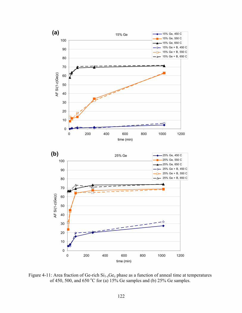
122
15% Ge
0
10
20
30
40
50
60
70
80
90
100
0 200 400 600 800 1000 1200time (min)
AF
Si(1
-z)G
e(z)
15% Ge, 450 C15% Ge, 550 C15% Ge, 650 C15% Ge + B, 450 C15% Ge + B, 550 C15% Ge + B, 650 C
25% Ge
0
10
20
30
40
50
60
70
80
90
100
0 200 400 600 800 1000 1200time (min)
AF
Si(1
-z)G
e(z)
25% Ge, 450 C25% Ge, 550 C25% Ge, 650 C25% Ge + B, 450 C25% Ge + B, 550 C25% Ge + B, 650 C
(a)
(b)
Figure 4-11: Area fraction of Ge-rich Si1-zGez phase as a function of anneal time at temperatures of 450, 500, and 650 oC for (a) 15% Ge samples and (b) 25% Ge samples.

123
Figure 4-12: Paired t-test results (n=36) comparing the undoped and doped samples at all conditions imaged with SEM/BSE for (a) Ge-rich Si1-zGez area fraction and (b) Ge-rich Si1-zGez grain size.

124
15% Ge
-3.5
-3
-2.5
-2
-1.5
-1
-0.5
0
0.5 1 1.5 2 2.5 3 3.5log(t)
log(
log(
1/(1
-AF)
))
15% Ge, 450 C15% Ge, 500 C15% Ge, 550 C15% Ge, 600 C15% Ge, 650 C15% Ge, 750 C15% Ge + B, 450 C15% Ge + B, 500 C15% Ge + B, 550 C15% Ge + B, 600 C15% Ge + B, 650 C15% Ge + B, 750 C
Figure 4-13: Plot of log(log(1/(1-AF))) vs. log(t) for samples containing 15% Ge
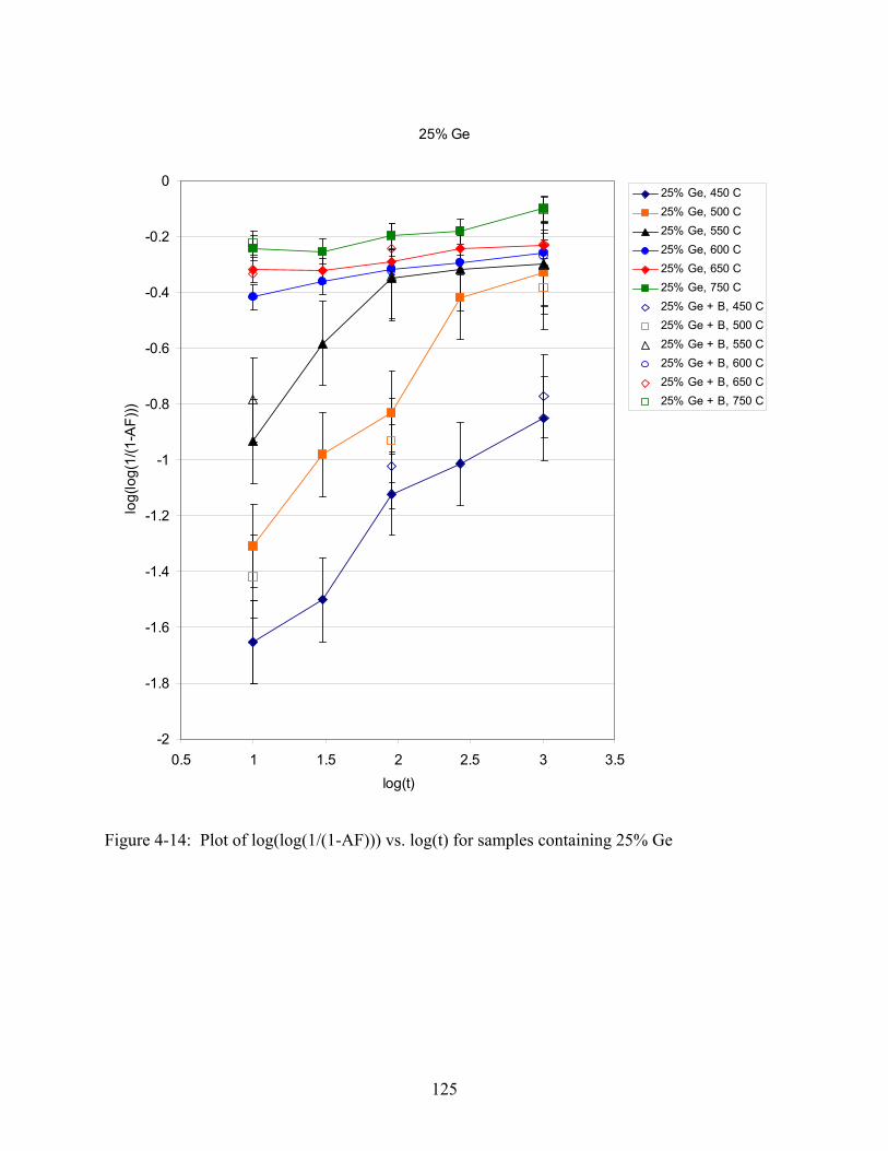
125
25% Ge
-2
-1.8
-1.6
-1.4
-1.2
-1
-0.8
-0.6
-0.4
-0.2
0
0.5 1 1.5 2 2.5 3 3.5log(t)
log(
log(
1/(1
-AF)
))
25% Ge, 450 C25% Ge, 500 C25% Ge, 550 C25% Ge, 600 C25% Ge, 650 C25% Ge, 750 C25% Ge + B, 450 C25% Ge + B, 500 C25% Ge + B, 550 C25% Ge + B, 600 C25% Ge + B, 650 C25% Ge + B, 750 C
Figure 4-14: Plot of log(log(1/(1-AF))) vs. log(t) for samples containing 25% Ge
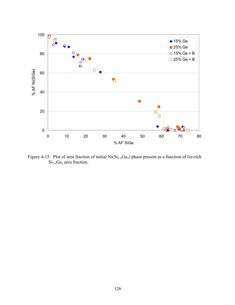
126
0
20
40
60
80
100
0 10 20 30 40 50 60 70 80% AF SiGe
% A
F N
i(SiG
e)
15% Ge25% Ge15% Ge + B25% Ge + B
Figure 4-15: Plot of area fraction of initial Ni(Si1-xGex) phase present as a function of Ge-rich Si1-zGez area fraction.
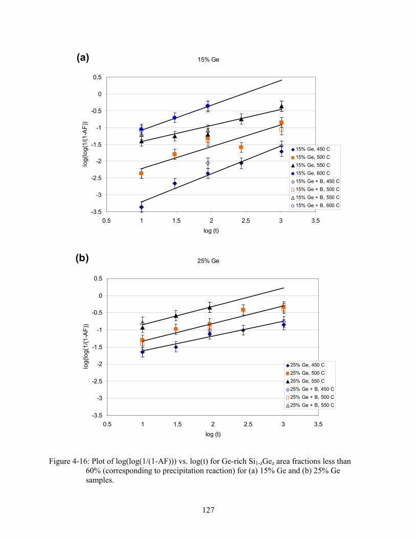
127
15% Ge
-3.5
-3
-2.5
-2
-1.5
-1
-0.5
0
0.5
0.5 1 1.5 2 2.5 3 3.5log (t)
log(
log(
1/(1
-AF)
)
15% Ge, 450 C15% Ge, 500 C15% Ge, 550 C15% Ge, 600 C15% Ge + B, 450 C15% Ge + B, 500 C15% Ge + B, 550 C15% Ge + B, 600 C
25% Ge
-3.5
-3
-2.5
-2
-1.5
-1
-0.5
0
0.5
0.5 1 1.5 2 2.5 3 3.5log (t)
log(
log(
1/(1
-AF)
)
25% Ge, 450 C25% Ge, 500 C25% Ge, 550 C25% Ge + B, 450 C25% Ge + B, 500 C25% Ge + B, 550 C
(a)
(b)
Figure 4-16: Plot of log(log(1/(1-AF))) vs. log(t) for Ge-rich Si1-zGez area fractions less than 60% (corresponding to precipitation reaction) for (a) 15% Ge and (b) 25% Ge samples.
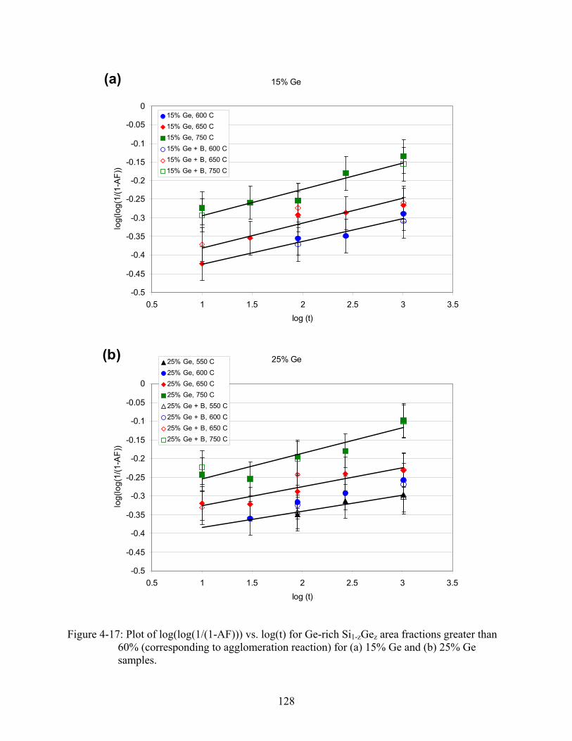
128
15% Ge
-0.5
-0.45
-0.4
-0.35
-0.3
-0.25
-0.2
-0.15
-0.1
-0.05
0
0.5 1 1.5 2 2.5 3 3.5log (t)
log(
log(
1/(1
-AF)
)15% Ge, 600 C15% Ge, 650 C15% Ge, 750 C15% Ge + B, 600 C15% Ge + B, 650 C15% Ge + B, 750 C
25% Ge
-0.5
-0.45
-0.4
-0.35
-0.3
-0.25
-0.2
-0.15
-0.1
-0.05
0
0.5 1 1.5 2 2.5 3 3.5log (t)
log(
log(
1/(1
-AF)
)
25% Ge, 550 C25% Ge, 600 C25% Ge, 650 C25% Ge, 750 C25% Ge + B, 550 C25% Ge + B, 600 C25% Ge + B, 650 C25% Ge + B, 750 C
(a)
(b)
Figure 4-17: Plot of log(log(1/(1-AF))) vs. log(t) for Ge-rich Si1-zGez area fractions greater than 60% (corresponding to agglomeration reaction) for (a) 15% Ge and (b) 25% Ge samples.

129
Activation Energy (Precipitation)
-11
-10
-9
-8
-7
-6
-5
-4
-3
-2
12 13 14 15 16 17 181/kT
ln(k
)
15% Ge25% Ge
(a)
1.96 eV
0.77 eV
Activation Energy (Agglomeration)
-1.5
-1.4
-1.3
-1.2
-1.1
-1
-0.9
-0.8
-0.7
-0.6
-0.5
10 11 12 13 14 151/kT
ln(k
)
15% Ge25% Ge
(b)
0.10 eV
0.14 eV
Figure 4-18: Plots of ln(k) vs. 1/(kT) for the (a) precipitation and (b) agglomeration reactions.
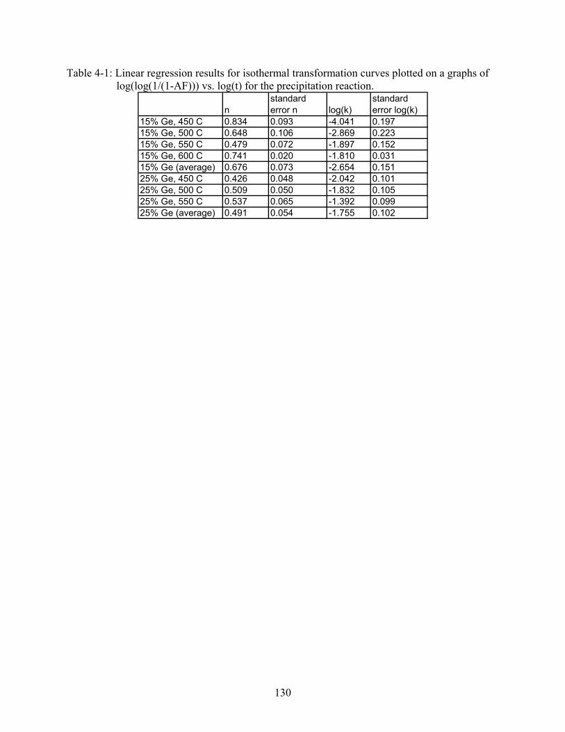
130
Table 4-1: Linear regression results for isothermal transformation curves plotted on a graphs of log(log(1/(1-AF))) vs. log(t) for the precipitation reaction.
nstandard error n log(k)
standard error log(k)
15% Ge, 450 C 0.834 0.093 -4.041 0.19715% Ge, 500 C 0.648 0.106 -2.869 0.22315% Ge, 550 C 0.479 0.072 -1.897 0.15215% Ge, 600 C 0.741 0.020 -1.810 0.03115% Ge (average) 0.676 0.073 -2.654 0.15125% Ge, 450 C 0.426 0.048 -2.042 0.10125% Ge, 500 C 0.509 0.050 -1.832 0.10525% Ge, 550 C 0.537 0.065 -1.392 0.09925% Ge (average) 0.491 0.054 -1.755 0.102
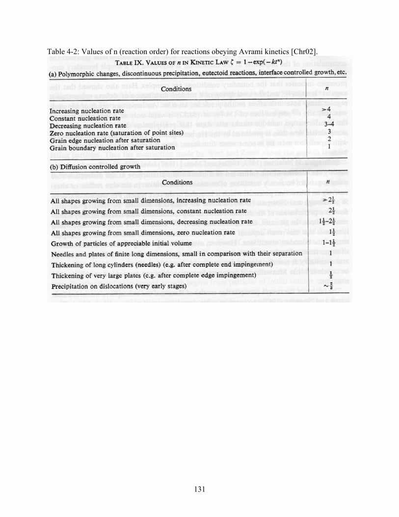
131
Table 4-2: Values of n (reaction order) for reactions obeying Avrami kinetics [Chr02].

132
Table 4-3: Linear regression results for isothermal transformation curves plotted on a graphs of log(log(1/(1-AF))) vs. log(t) for the agglomeration reaction
nstandard error n log(k)
standard error log(k)
15% Ge, 600 C 0.061 0.012 -0.485 0.03015% Ge, 650 C 0.067 0.014 -0.448 0.02915% Ge, 750 C 0.071 0.009 -0.366 0.02015% Ge (average) 0.066 0.012 -0.433 0.02625% Ge, 550 C 0.043 0.006 -0.428 0.01625% Ge, 600 C 0.060 0.005 -0.442 0.01225% Ge, 650 C 0.051 0.009 -0.377 0.01925% Ge, 750 C 0.068 0.011 -0.323 0.02425% Ge (average) 0.056 0.008 -0.392 0.017
Agglomeration

133
Table 4-4: Activation energies derived from linear regression of series on the plot of ln(k) vs. (1/KT)
Ea s.e. Ea15% Ge -1.961 0.37625% Ge -0.765 0.186
Ea s.e. Ea15% Ge -0.143 0.00925% Ge -0.100 0.029
Precipitation
Agglomeration

134
CHAPTER 5 RELATIONSHIP OF SHEET RESISTANCE AND MICROSTRUCTURE AND THE
INFLUENCE OF GE AND B
This chapter explores the influence of both Ge content and homogeneous in-situ B doping
of the initial Si1-xGex layer on the sheet resistance of nickel germanosilicide thin films. Using the
results from the quantitative microstructure analysis performed in the previous chapter, this
chapter also investigates the structure/property relationship between sheet resistance and
microstructure. The influence of Ge content and B doping on the relationship is also addressed.
Prior work has widely utilized four point probe (4PP) sheet resistance measurements to
characterize the electrical quality of nickel germanosilicide thin films. Isochronal sheet
resistance measurements of undoped films, such as the one previously shown in Figure 2-19,
have been reported by many researchers [Pey02, Zha02, Cha04, Cha04b, Zha04, Seg04, Liu05,
Cho06, Ko06, Lau06, Yao06]. In each case, the isochronal sheet resistance curves show a
relatively sharp increase in value around ~700 oC. In the absence of a high-resistivity
digermanosilicide (analogous to the NiSi2 phase), this increase is attributed to the agglomeration
of the film. However, due to the limited thermal matrix and common lack of quantitative
microstructure analysis, any direct structure/property relationship between sheet resistance and
the microstructure has not been established.
Also of interest is determining how both Ge content and homogeneous in-situ B doping of
the initial Si1-xGex layer may affect the structure/property relationship. While it has been
established in prior work [Ok03, Zha04] and confirmed in the previous chapter of this work that
increasing Ge content increases film agglomeration, it is unknown whether Ge content would
affect any microstructure/sheet resistance relationship. Prior work by Liu and Ozturk [Liu05]
has shown that incorporation of high levels of in-situ doped B stabilizes sheet resistance. Their
explanation for the cause of the stabilization (a reduction in agglomeration), however, was not
135
seen in the B doped samples of this work. Thus, it is of interest to first determine whether
similar stabilization occurred in the samples in this work and, if so, how any structure/property
relationship between sheet resistance and microstructure may have been altered.
To investigate the sheet resistance, structure/property relationship, and influence of Ge and
B, the nickel germanosilicide films were formed at a range of thermal conditions. The Ge
content in the initial Si1-xGex layer of the structures was varied at levels of 10 and 25 at% and the
layers were undoped or incorporated ~4.5E19 atoms/cm3 of homogeneous in-situ B doping. The
samples were annealed in a quartz tube furnace under N2 ambient at temperatures between 450
and 800 ºC in increments of 50 ºC for 10, 30, 90, 270, and 1020 minutes. Once annealed, the
sheet resistance of the samples was measured using a 4PP and the method previously presented
in Chapter 3. It should be noted that, with the exceptions of the additional thermal series at 700
and 800 oC, the samples from the previous chapter were used for the analysis presented in this
chapter.
5.1 Sheet Resistance Analysis
The sheet resistance of all samples was measured using the 4PP method outlined in
Chapter 3. In keeping with prior work, the values of sheet resistance were plotted as a function
of anneal temperature (isochronal series). It is important to note, however, that all samples were
not able to be successfully measured for all times and temperatures. Instead, at higher values of
temperature (generally over ~600 oC), some undoped samples were determined to be
nonconductive. In this case, the plots of sheet resistance for those samples show a dashed line
extrapolating to infinity after the last successful measurement of the isochronal series. The
following sections discuss the sheet resistance measurement results in terms of Ge and B content
to determine the respective influences of each variable.
136
5.1.1 Influence of Ge
The sheet resistance measurements for the undoped 15 and 25% Ge samples are presented
in Figure 5-1(a) as a function of anneal temperature (isochronal series). Only the 10, 90, and
1020 minute anneal series are shown for clarity. It is apparent from the plot that increasing Ge
content caused earlier increases in sheet resistance for all anneal series. The difference between
the sheet resistances at each point in the thermal matrix was also calculated by subtracting the
sheet resistance value of the 15% Ge sample from that of the 25% Ge sample, shown in Figure 5-
1(b) for the isochronal 10, 90, and 1020 minute series. Dotted lines in the figure represent
extrapolation to infinite sheet resistance (i.e. the next point in the series was unable to be
successfully measured). It is evident from this plot that increasing Ge content increased the sheet
resistance of the film by 10s to 100s of Ohm/sq. The intermediate isochronal series that were not
shown in Figure 5-1 (30 and 270 min) displayed similar trends. The trend seen in these results
agree well with those shown in prior work, where increasing Ge content was shown to result in
poorer thermal stability of sheet resistance [Ok03, Zha04].
Isochronal sheet resistance measurements for the doped 15 and 25% Ge samples are
presented in Figure 5-2(a). As with the undoped case, only the 10, 90, and 1020 minute anneal
series are shown for clarity. It is apparent from the plot that, similar to the undoped samples,
increasing Ge content caused an increase in sheet resistance for all anneal series. Figure 5-2(b)
plots the differences between the sheet resistance values of the 25 and 15% Ge samples. It is
evident from this plot that increasing Ge content increased the sheet resistance of the film by ~2
to ~70 Ohm/sq. In comparison with the undoped samples, these increases were generally smaller
and more consistent across the thermal matrix. The intermediate isochronal series that were not
shown in Figure 5-2 (30 and 270 min) displayed similar trends. This experiment was the first
time the effect of Ge content on samples with homogeneously B doped Si1-xGex layers was

137
investigated; the work by Liu and Ozturk [Liu05] did not vary Ge concentration (though it did
vary initial Ni layer thickness). It is important to observe, therefore, that the trend of increasing
Ge content increasing sheet resistance seen in undoped samples is also present in the doped
samples, though to a lesser degree.
5.1.2 Influence of B
Previous work has shown that the addition of dopants to the initial Si1-xGex prior to
silicidation may [Liu05] or may not [Cha04] affect the sheet resistance of nickel germanosilicide
thin films. Isochronal sheet resistance measurements for the undoped and doped 15% Ge
samples in this work are presented in Figure 5-3(a). Only the 10, 90, and 1020 minute anneal
series are shown for clarity. It is apparent from the plot that the B doped samples have a lower
sheet resistance than the corresponding undoped samples at all times and temperatures. It is also
apparent that the addition of B stabilized the sheet resistance measurements to much higher
temperatures; as previously shown, no doped sample registered as non-conductive in this work.
Figure 5-3(b) plots the differences between the sheet resistance values of the doped and undoped
15% Ge samples. It is evident from this plot that the addition of B doping initially provides a
small decrease in sheet resistance. However, once the sheet resistance of the undoped sample
begins to rapidly increase the addition of B doping results in a large decrease of sheet resistance.
The magnitude of the decrease was eventually equal to infinity as the undoped samples read as
open circuits and the doped samples maintained values less than ~120 Ohm/sq. The intermediate
isochronal series that were not shown in Figure 5-2 (30 and 270 min) displayed similar trends.
Isochronal sheet resistance measurements for the undoped and doped 25% Ge samples are
presented in Figure 5-4(a) and their differences in (b). These results are very similar to those
discussed for the undoped and doped 15% Ge samples with the exception that the stabilization
begins earlier (due to the influence of Ge content). As with the 15% Ge samples, the addition of
138
B stabilized the sheet resistance measurements to much higher temperatures. The difference
between the sheet resistances of corresponding undoped and doped samples was also initially
small and then rapidly grew, approaching infinity.
These results confirm that both the 15 and 25% Ge structures used in this work show the
stabilizing effect on sheet resistance of the addition of high levels of homogeneous B doping
during Si1-xGex layer growth reported by Liu and Ozturk [Liu05]. While the level of B doping in
this work (~4.5E19 atoms/cm3) is less than that used in their published work (~2.1E21
atoms/cm3), it is reasonable to assume that the same mechanism is causing the reduction and
stabilization of sheet resistance for both works. Liu and Ozturk proposed that the cause for the
effect was due to a reduction in agglomeration caused by strain-reliving effects of the high levels
of B. The previous chapter of this work, however, showed that no difference in sample
microstructure or evolution was caused by the addition of B doping. Thus, the effects of B on
sheet resistance cannot be explained by its influence on film microstructure. A different
proposed mechanism, and the influence of B doping on any sheet resistance/microstructure
relationship, will be discussed in the following sections.
5.2 Sheet Resistance/Microstructure Relationship
Apart from the specific influences of Ge and B content, Figures 5-1 to 5-4 show a general
trend of increasing thermal annealing causing an increase in sheet resistance (to a greater or
lesser degree. dependent on Ge and B content). Similar trends have been extensively reported in
literature and are generally ascribed to the worsening of film morphology with increasing anneal
time and temperature (e.g. �“agglomeration�”) [Pey02, Zha02, Cha04, Cha04b, Zha04, Seg04,
Liu05, Cho06, Ko06, Lau06, Yao06]. In general, however, prior literature has lacked
quantitative analysis of film morphology in plan view, as well as having been confined to a
single isochronal series. These limitations have precluded establishment of any direct,
139
quantitative structure/property relationship between film morphology and sheet resistance.
Instead, only a circumstantial, qualitative relationship has been established. This work, however,
performed quantitative microstructure analyses of a large number of anneal times and
temperatures. These results, presented in the previous chapter, can be used in conjunction with
the corresponding sheet resistance measurements presented in the preceding sections of this
chapter to investigate the structure/property relationship between film microstructure and sheet
resistance in a quantitative manner.
Film microstructures in Chapter 4 were quantified using three metrics: Ge-rich Si1-zGez
grain size, Si-rich Ni(Si1-uGeu) area fraction, and Ge-rich Si1-zGez area fraction. Each of these
three metrics was evaluated for suitability in establishing a structure/property relationship by
plotting the sheet resistance of each sample as a function of the metric. Figure 5-5 presents the
result of plotting sheet resistance as a function of Ge-rich Si1-zGez grain size for all four structure
types. Analysis of the plot shows that data from each sample type is widely scattered and
intermixed with the other types, no discernable patterns are apparent. It is evident from this
figure that Ge-rich Si1-zGez grain size is not a suitable metric for establishing a quantitative
relationship. Next, sample sheet resistance was plotted as a function of Si-rich Ni(Si1-uGeu) area
fraction, shown in Figure 5-6(a). While this plot shows stronger trends than Figure 5-5,
consistent relationships are not readily observed. Finally, sample sheet resistance was plotted as
a function of Ge-rich Si1-zGez area fraction, shown in Figure 5-6(b). This plot shows strong,
consistent trends for all sample series which are clearly superior to those generated using the
other metrics. It was determined, therefore, that Ge-rich Si1-zGez area fraction was the best
metric for use in establishing a structure/property relationship. It should be noted that Figure 5-
6(b), and the plots derived from it throughout this chapter, is a plot of two experimentally
140
measured parameters. Accordingly, each data point has error in both the x (Ge-rich Si1-zGez area
fraction) and y (sheet resistance) axes of the plot. For the x-axis, error remains as discussed
previously and in Appendix A, with a 95% confidence interval of 3.35%. The y-axis error, as
determined in Appendix B, however, is narrow enough in range (~2.2 Ohm/sq for a 95%
confidence interval) in comparison to the magnitude of the measurements that the error bars are
not visible on the plot.
It is clearly evident from Figure 5-6(b) that a structure/property relationship between Ge-
rich Si1-zGez area fraction and film sheet resistance can be established. Both area fraction and
sheet resistance are area properties. Hence, it could be expected that the sheet resistance of an
anisotropic, non-textured two-phase microstructure (such as that evident in the SEM/BSE images
of Figures 4-5 to 4-8) would vary linearly between the values of each phase. This relationship,
however, is clearly not shown by the series in Figure 5-6(b). The discrepancy can be further
illustrated by Figure 5-7(a), which shows the experimental relationship for the doped 15% Ge
samples versus a linear interpolation between the values for the homogeneous nickel
germanosilicide film (~10 Ohm/sq) and the B-doped Si1-xGex layer (~120 Ohm/sq).
While, on initial observation, it may be attractive to model the microstructure/sheet
resistance relationships for the sample series as exponential functions, the results from the
microstructure analysis performed in Chapter 4 should be considered first. It was previously
shown in Figure 4-15 that the area fraction of the initial Ni(Si1-xGex) phase decreases with
increasing Ge-rich Si1-zGez area fraction. If this same plot is added on a secondary axis to a plot
of the structure/property relationships, as is shown in Figure 5-7(b), it can be seen that the
inflection point in the relationship corresponds to the disappearance of the initial Ni(Si1-xGex)
phase (at ~60% area fraction of Ge-rich Si1-zGez) . The analysis in Chapter 4 also showed that it
141
is at this point that the morphological evolution of the film should be separated into two stages:
precipitation and agglomeration. With this consideration, it is apparent that the
structure/property relationships should be modeled as two sets of linear functions, one for each
of the stages of microstructure evolution. These two stages, called Stage I for the precipitation
reaction and Stage II for the agglomeration reaction, are shown in Figure 5-7(b). These
structure/property relationships, and the influence of Ge and B on them, will be discussed in the
following sections.
5.2.1 Stage I (Precipitation)
Figure 5-8 presents the sheet resistance of the sample series as a function of Ge-rich Si1-
zGez area fraction for area fractions less than 60%, corresponding to the precipitation stage of the
microstructure evolution process. It is evident from this figure that the distribution of data points
is not even, but skewed towards lower area fractions (less than ~25%). This is a result of the
anneal sequences not being tailored to produce evenly spaced steps in area fractions, as the
necessary rate calculations to engineer such a spacing were not available. It is also evident from
the figure that there appears to be more spread in the data as the area fraction increases. Both of
these observations will become important in the following sections as the influences of Ge and B
are considered.
5.2.1.1 Influence of Ge
The influence of initial Si1-xGex layer Ge content on the structure/property relationship of
the undoped samples was determined by plotting the area fraction of Ge-rich Si1-zGez area
fraction versus sheet resistance, shown in Figure 5-9(a). Linear regression analysis of the series
was also performed and the best fit lines shown on the plot. The linear regression analysis
provided a best fit line with an R2 value of 0.7454 and 0.8431 for the 15 and 25% Ge samples,
respectively. The regression results including slope, slope standard error, intercept, and intercept
142
standard error, are presented in Table 5-1. These results, in combination with the R2 values,
indicate that the accuracy of the linear regressions for the undoped samples are hampered by the
relatively few data points and large scatter above ~25% Si1-zGez area fraction, especially for the
15% Ge samples. Nevertheless, it can be concluded that increasing Ge-rich Si1-zGez area fraction
causes an increase in sheet resistance.
Figure 5-9(b) presents a plot of the area fraction of Ge-rich Si1-zGez area fraction versus
sheet resistance for the doped 15 and 25% Ge samples. As with the undoped samples, linear
regression analysis was performed and the best fit line shown for each series, with R2 values of
0.8663 and 0.8423 for the 15 and 25% Ge series, respectively. The numerical regression results
for these lines are also given in Table 5-1. These results indicate that the doped samples have a
stronger linear trend than their undoped counterparts. Less disparity between the regression lines
for the two series is also qualitatively apparent for the doped samples when compared to the
undoped ones. As with the undoped series, however, the accuracy of the results is still hampered
by the relative scarcity of data between ~25 and 60% Ge-rich Si1-zGez area fraction, especially
for the 15% Ge samples.
The values for the regression intercepts and their 95% confidence intervals are shown in
Figure 5-10(a) and for each of the four sample series. Using 2-sample t-tests, it can be shown
that no statistically significant differences in intercept value exist at the 95% confidence level
between any of the sample series. This result was expected, as at low times and temperatures all
samples exhibited a homogeneous, continuous film of Ni(Si1-x)Gex. It would be expected,
therefore, that the intercept value of each plot of area fraction Ge-rich Si1-xGex vs. sheet
resistance would be equal to each other and the sheet resistance of this initial film (where there is
0% area fraction Si1-zGez). The average intercept value of ~8 +/- 3 Ohm/sq does in fact agree

143
well with the previously reported values for a such a film which have usually averaged between
5 and 12 Ohm/sq dependent upon initial Ni layer thickness, etc [Ok03, Cha04, Zha04, Liu05].
The values for the regression slopes and their 95% confidence intervals are shown in
Figure 5-10(b) and for each of the four sample series. While 2-sample t-tests cannot statistically
prove that the slopes for the 15 and 25% Ge samples are equivalent, this is likely due to the
uncertainty introduced by the aforementioned scatter and lack of data at area fractions between
25 and 60%, especially for the 15% Ge samples. Qualitatively, however, the slope regression
results for the 15 and 25% Ge series appear to be fairly similar for either the undoped or doped
samples. These observations are further reinforced by observation of Figure 5-9(a) and (b)
where the data points for both the 15 and 25% Ge samples appear to be well-interspersed for
both the undoped and doped samples. It can be tentatively concluded, therefore, that increasing
Ge content of the initial Si1-xGex layer does not affect the structure/property relationship between
precipitated Ge-rich Si1-zGez area fraction and sheet resistance. This conclusion, however,
requires further experimentation to provide statistically significant support; the needed
experimentation will be discussed in a later section.
5.2.1.2 Influence of B
Figure 5-11 presents a plot of film sheet resistance vs. Ge-rich Si1-zGez area fraction for all
four sample series. The analysis in the previous section showed that it can be tentatively
concluded that varying Ge content in undoped and doped nickel germanosilicide thin films does
not affect the relationship between film morphology and sheet resistance. This section,
therefore, grouped together the data from the 15 and 25% Ge samples when considering the
influences of homogeneous B doping of the initial Si1-xGex layer on the structure/property
relationship. Linear regression analysis was accordingly performed on the grouped 15 and 25%
Ge samples for the undoped and doped cases and the best fit regression lines shown on Figure 5-
144
11. The numerical regression results are included in Table 5-2 and the regression intercepts,
slopes, and respective 95% confidence intervals of the lines are presented in Figure 5-12(a) and
(b).
Comparison of the regression intercept values with a 2-sample t-test shows that there is no
difference between the undoped and doped samples at a 95% confidence level. As in the
previous section, the average intercept value of 9.7 +/- 2 Ohm/sq agrees well with prior
literature. Comparison of the regression slope values, however, shows that there is a significant
difference between the undoped and doped samples at a 95% confidence level with the doped
samples having a slope approximately ~60% less than the undoped samples. It can be
concluded, therefore, that the addition of homogeneous B doping influences the fundamental
structure/property relationship between film microstructure and sheet resistance. The cause for
this influence is likely the addition of a more conductive current path provided by the B doped
samples. The specific nature and location of this conductive path will be addressed separately in
a later section.
5.2.1.3 Tortuosity Analysis
The previous sections have established that the sheet resistance of nickel germanosilicide
thin films increases approximately linearly with increasing Si1-zGez area fraction within this stage
of the overall microstructure evolution (less than 60% AF Si1-zGez). Figure 5-7(a) has previously
shown, however, that the effect cannot be described by a liner interpolation between the sheet
resistance of the initial film and the substrate. It is of interest, therefore, to determine the if the
underlying cause for the relationship can be determined.
When considering possible mechanisms, it is important to remember that the defining
characteristic of the first stage of the microstructure evolution is the presence of initial Ni(Si1-
xGex) phase which has not yet fully rejected Ge and transformed into Si-rich Ni(Si1-uGeu) and
145
Ge-rich Si1-zGez. Thus, it can be qualitatively observed in the SEM/BSE images that within this
stage, the highly conductive Ni(Si1-xGex) and Si-rich Ni(Si1-uGeu) phases form a continuous
network which is disrupted by grains of relatively less conductive Ge-rich Si1-zGez. This
observation leads to the suggestion that the conductive phases may be carrying the majority of
the current and that the less conductive Ge-rich Si1-zGez grains are disrupting the current path,
causing an increase in sheet resistance with increasing area fraction (and hence interference) of
Si1-zGez.
It was of interest, therefore, to determine how the conductive path tortuosity and the area
fraction of Si1-zGez were related. Accordingly, the tortuosity of selected doped and undoped
25% Ge samples was calculated according to the method described in Chapter 3. Figure 5-13
shows a example image and estimated continuous conductive path across the sample. The
samples used in this analysis, and their Si1-zGez area fraction, tortuosity, and sheet resistance are
presented in Table 5-3. The samples were selected such that the covered the entire range of Si1-
zGez area fractions within the first stage of microstructure transformation. It is important to note
that, due to the requirement of manual calculation, sample tortuosity was calculated using the
average of three random measurements of a single image for each sample condition. The small
sample size and relatively inaccurate calculation (when compared to computer modeling),
therefore, resulted in substantial error in the tortuosity measurement. The average tortuosity
range for the three measurements of each image was determined to be 0.0333. The measurement
error, therefore, was estimated by dividing this value by the square root of the sample size (3)
according to the work of Kyker [Kyk83] which showed that for normal distributions, this
calculation would estimate the true standard deviation within 10-15%. For the tortuosity

146
calculations in this work, the resulting 95% confidence interval based on the error estimation
proposed by Kyker was determined to be +/- 0.0377.
Figure 5-14(a) presents a plot of conductive path tortuosity vs. Si1-zGez area fraction for the
selected undoped and doped 25% Ge samples. It is evident from this plot that conductive path
tortuosity increases linearly with increasing area fraction of Si1-zGez. It is also apparent without
statistical analysis that B doping does not influence the relationship between the two properties.
A single linear regression was therefore performed for all data points and the best fit regression
line and equation shown in the figure. While the tortuosity of the 15% Ge samples was not
studied, the same relationship is expected due to the similarity in microstructure evolution
observed in the previous chapter. Additional work should be performed, however, to confirm
this expectation and strengthen the observed relationship by reducing the error in tortuosity
measurement.
The direct relationship between tortuosity and sheet resistance was also explored; the sheet
resistance of the undoped and doped 25% Ge samples was plotted as a function of conductive
path tortuosity and is presented in Figure 5-14(b). While observation of this plot shows that
there is a distinct relationship between the two properties, it is not evident (due to the few data
points and large error) either through qualitative or statistical analysis whether the relationship is
of an exponential nature or linear relationship. The R2 values for an exponential relationship are
0.864 and 0.874 for the undoped and doped 25% Ge samples, respectively. For a linear
relationship, the values are 0.830 and 0.817, respectively. Regardless, the stabilization caused by
B doping is clearly evident in the figure as the doped samples have smaller sheet resistance
values than the undoped samples of equal tortuosity. While additional analysis is necessary to
better establish the relationship, these results support the theory that the mechanism behind the
147
structure/property relationship in this stage of the film�’s microstructural evolution is likely
related to the disruption of the conductive path through the Ni(Si1-xGex) and Si-rich Ni(Si1-uGeu)
grains by the precipitation of less conductive Si1-zGez. It is also probable, therefore, that the
addition of B doping reduces the magnitude of this disruption by providing an alternative
conduction path; as mentioned before, the nature and location of this path will be addressed in a
later section. It is also important to note that the linear relationship between conductive path
tortuosity and Si1-zGez area fraction suggests that the properties may be co-dependant variables.
If so, conductive path tortuosity may be a better predictor of sheet resistance than Si1-zGez area
fraction.
5.2.2 Stage II (Agglomeration)
The structure/property relationship between film microstructure and sheet resistance was
also considered within the agglomeration stage of the film transformation. The samples in this
stage had Si1-zGez area fractions above 60% and no sample in the study exhibited an area fraction
greater than 78.16%. It is expected, however, that samples with significantly greater area
fractions than this value will not occur, as while Ni(Si1-uGeu) grains are agglomerating in this
stage to reduce their interface energies resulting in the deepening of grains and through
conservation of mass an associated reduction in projected size, eventually an equilibrium will be
reached in this process. More simply put, the area fraction of Si1-zGez will never reach 100% as
long as grains of Ni(Si1-uGeu) are present in the film. Thus, the analyses in the following
sections, which consider the influences of Ge and B, are likely representative of the entire
reaction stage and not just a single segment or subset thereof.
5.2.2.1 Influence of Ge
Figure 5-15(a) presents a plot of the sheet resistance of the undoped 15 and 25% Ge
samples as a function of Si1-xGez area fraction. Error ranges are omitted for clarity. The data in
148
this plot, which is shown on a logarithmic plot due to the substantial disparity in sheet resistance
measurements, shows a wide degree of scatter for the 25% Ge samples. Additionally, only two
data points are included for the 15% Ge samples. The scarcity of data may be attributed to the
fact that the sheet resistance of only two of the ten 15% Ge samples with Si1-xGez area fractions
contained in this stage of the reaction was able to be successfully measured. Likewise, only ten
of the seventeen 25% Ge samples were able to be measured. The cause for this difficulty will be
addressed in the following section. It should also be noted that the analysis in Appendix B
showed that 4PP measurement of sheet resistances above ~500 Ohm/sq showed much greater
variability than those at lower values. Accordingly, no influence of Ge content may be
determined for the undoped samples.
Figure 5-15(b) presents a plot of the sheet resistance of the doped 15 and 25% Ge samples
as a function of Si1-xGez area faction with error bars omitted for clarity. It is evident from this
plot that the sheet resistance of the doped samples in this range has a linear relationship with Si1-
xGez area fraction. Accordingly, linear regression of the data series was performed; the best fit
lines are shown in the figure and the regression results given in Table 5-4. Analysis of the
regression results using a 2 sample t-test shows that the slope and intercept of the best fit lines
for the doped 15 and 25% Ge are not equal at a 95% confidence level. Thus, it can be concluded
that, unlike within the first transformation stage, increasing Ge content in this stage affects the
structure/property relationship.
5.2.2.2 Influence of B
Figure 5-16 presents a plot of the sheet resistance of all four sample series as a function of
Si1-zGez area fraction. It should be noted that a log scale was used for the y-axis of the plot
(sheet resistance) to display all data points within reasonable proximity and that error bars were
omitted for clarity. Observation of this figure shows that the doped samples have much smaller
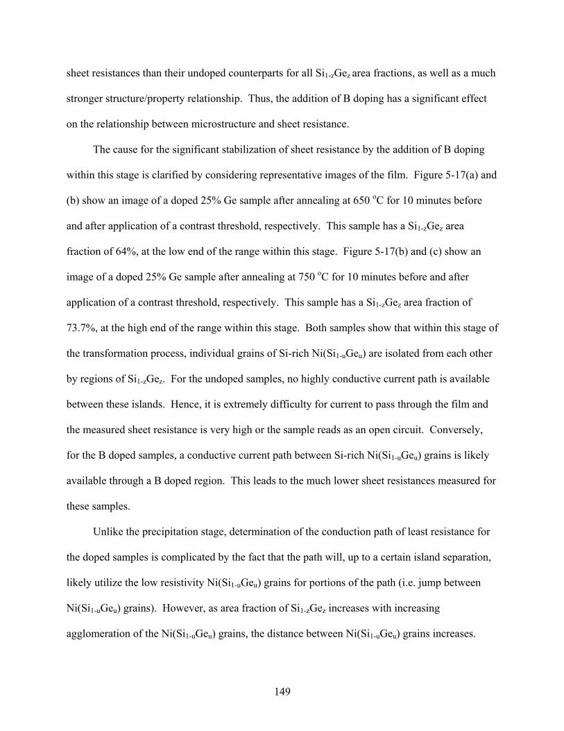
149
sheet resistances than their undoped counterparts for all Si1-zGez area fractions, as well as a much
stronger structure/property relationship. Thus, the addition of B doping has a significant effect
on the relationship between microstructure and sheet resistance.
The cause for the significant stabilization of sheet resistance by the addition of B doping
within this stage is clarified by considering representative images of the film. Figure 5-17(a) and
(b) show an image of a doped 25% Ge sample after annealing at 650 oC for 10 minutes before
and after application of a contrast threshold, respectively. This sample has a Si1-zGez area
fraction of 64%, at the low end of the range within this stage. Figure 5-17(b) and (c) show an
image of a doped 25% Ge sample after annealing at 750 oC for 10 minutes before and after
application of a contrast threshold, respectively. This sample has a Si1-zGez area fraction of
73.7%, at the high end of the range within this stage. Both samples show that within this stage of
the transformation process, individual grains of Si-rich Ni(Si1-uGeu) are isolated from each other
by regions of Si1-zGez. For the undoped samples, no highly conductive current path is available
between these islands. Hence, it is extremely difficulty for current to pass through the film and
the measured sheet resistance is very high or the sample reads as an open circuit. Conversely,
for the B doped samples, a conductive current path between Si-rich Ni(Si1-uGeu) grains is likely
available through a B doped region. This leads to the much lower sheet resistances measured for
these samples.
Unlike the precipitation stage, determination of the conduction path of least resistance for
the doped samples is complicated by the fact that the path will, up to a certain island separation,
likely utilize the low resistivity Ni(Si1-uGeu) grains for portions of the path (i.e. jump between
Ni(Si1-uGeu) grains). However, as area fraction of Si1-zGez increases with increasing
agglomeration of the Ni(Si1-uGeu) grains, the distance between Ni(Si1-uGeu) grains increases.

150
This effect is shown in the SEM/BSE images of the microstructure; the sample in Figure 5-17(a)
with area fraction of 64% is clearly less agglomerated than the sample in Figure 5-17(c) with
area fraction of 73.7%. The increasing separation between highly conductive grains will
therefore cause the observed increase in sheet resistance with Si1-zGez area fraction as an
increasing percentage of the total conduction path is spent between the Ni(Si1-uGeu) grains.
Eventually, this path may become so tortuous that it becomes favorable for it to pass directly
through the B doped regions and intersect only the Ni(Si1-uGeu) grains which happen to lie on a
line directly along the chord of the path (i.e. directly between the terminals of a 4PP). If this
occurs, it would be expected that the plot of sheet resistance vs. Si1-zGez area fraction would
show an inflection point as the relationship would become relatively insensitive to
agglomeration. While no such point is visible in Figure 5-15(b), it is possible that the Si1-zGez
area fractions obtained in this work are not large enough. Additional work should be performed,
therefore, to see if such a point exists at area fractions greater than 75%.
5.2.3 Boron Conduction Path
Prior sections of this chapter have suggested that doped regions of the experimental
structures containing homogeneous B doping are providing an alternative conduction path for
current flow, thereby reducing the sheet resistance of the film. In some cases, such as during the
precipitation reaction, the amount of reduction is relatively low. In other cases, such as during
the agglomeration reaction, the amount of reduction is large (even approaching infinity). The
nature and location of the alternative path, however, has not yet been addressed.
Published literature has shown that full silicidation (FUSI) of doped polysilicon gates
using Ni metal can lead to improved device performance through tuning of the gate work
function and reduction of gate tunneling effects [Mas05]. The improvements are attributed to
silicidation induced dopant segregation leading to high concentrations of dopants in proximity to

151
the gate oxide. Specifically, literature has shown that nickel silicidation of a B implanted Si
sample past the initial implant depth results in the pile-up of B at the silicide/silicon interface.
Zhang et al. performed an experiment where a 2 keV 3E15 atoms/cm2 B implant was performed
into bulk silicon resulting in an initial peak concentration 10 nm below the sample surface. After
deposition of excess Ni metal, the implanted samples were annealed at 500 oC for 90 seconds
under a N2 atmosphere. The samples were then analyzed using SIMS; the results are shown in
Figure 5-18. It is evident from this figure that silicidation induced dopant segregation has moved
the peak dopant concentration from a depth of ~10 nm to ~80 nm leaving only residual B doping
of the silicide.
Silicidation induced dopant segregation has not been studied in the nickel germanosilicide
system. It is plausible, however, to expect that similar segregation occurs in this system as well.
To determine if any dopant segregation was observed in the B doped samples in this work, SIMS
analysis of the doped 25% Ge sample annealed at 450 oC for 10 minutes was performed. This
sample was selected for analysis as it has the most homogeneous layer compositions (beneficial
for SIMS analysis) and any silicidation induced dopant segregation would have already occurred
(as the segregation would occur during the formation of the silicide layer). An XTEM image of
the sample is presented in Figure 5-19(a) and the SIMS results are shown in Figure 5-19(b).
While evidence of dopant segregation is apparent in the SIMS results, due to the interface
roughness observed in the XTEM image the SIMS results are of overall poor quality (as
evidenced by the large concentration tails). Thus, another technique less susceptible to interface
effects should be used to confirm the presence of dopant segregation.
5.2.3.1 Potential Conduction Paths
Assuming that silicidation induced dopant segregation does occur for the B doped samples
in this work, three potential conduction paths can be proposed for the structure. As shown in
152
Figure 5-20, silicidation induced dopant segregation would result in a residually doped nickel
germanosilicide silicide layer, the first possible conduction path. Assuming that the segregated
B doping is fully electrically active (which is conservative, as it the mechanism by which
segregation occurs is not understood), the region with the segregated dopant would form a
second path. Finally, the unreacted, actively doped Si1-xGex layer will offer a third conduction
path.
The potential sheet resistance of each of the three potential conduction paths was estimated
for the doped 15% Ge sample. The sheet resistance of the doped 15% Ge sample annealed at
450 oC for 10 minutes was measured to be ~10 Ohm/sq. This value is accordingly
approximately equal to the sheet resistance of a 20 nm homogeneous nickel germanosilicide
layer. A wafer without deposited Ni was also available for this experimental structure; 4PP
measurement of this wafer�’s 150 nm B doped Si0.85Ge0.15 layer showed that the sheet resistance
of the layer was 120 Ohm/sq. Sheet resistance (Rs) and sample resistivity ( ) are related
according to Equation 5-1 when the ratio of sample length (L) to width (W) is equal to 1.
)(WL
tRs Equation 5-1
Equation 5-1 shows, therefore, that dividing the sheet resistance of the layer by its thickness (150
nm) allowed the resistivity of the layer to be calculated as 1.8E-5 Ohm*m. As the resistivity of a
semiconductor is inversely proportional to its level of doping, assuming that all segregated
dopant from the ~20 nm germanosilicide layer is contained within a 10 nm layer below the
interface, the layer containing the pileup of segregated dopant would have three times the
nominal dopant concentration and thus an estimated resistivity of 6E-6 Ohm*m (one-third of the
nominal resistivity). The estimated sheet resistance of the region with the pileup of segregated
dopant can accordingly be calculated as ~600 Ohm/sq. The estimated sheet resistance of the
153
remaining 120 nm layer of unreacted, nominally B doped Si0.85Ge0.15 layer would then be equal
to 150 Ohm/sq (due to its reduced thickness). It should also be noted that if the dopant pileup
caused by silicidation induced dopant segregation is not electrically active, the expected sheet
resistance of the remaining 130 nm of nominally B doped Si0.85Ge0.15 would have a sheet
resistance of 140 Ohm/sq.
Comparison of the calculated sheet resistance values for the 10 nm region with the pileup
of segregated B dopant and the remaining 120 nm of unreacted, nominally B doped Si0.85Ge0.15
layer indicates that, while the concentration of active dopant in the region with pileup is
potentially 3 times higher than that of the unreacted, nominally doped layer, the differences in
layer thicknesses cause the sheet resistance of the region with pileup to be significantly higher
(600 Ohm/sq. vs. 150 Ohm/sq, respectively). When considered as resistors in parallel, however,
the combined resistance of the two layers decreases to 120 Ohm/sq according to Equation 5-2:
21
111
RR
Rparallel Equation 5-2
Thus, if pileup of active dopant does occur due to silicidation induced dopant segregation, the
measured sheet resistance of the non-germanosilicide layers would be expected to be ~120
Ohm/sq. If pileup does not result in increased amounts of active dopant, the measured sheet
resistance of the non-germanosilicide layers would be expected to be ~140 Ohm/sq (equal to the
sheet resistance of 130 nm of nominally dopes Si0.85Ge0.15).
5.2.3.2 Evaluation of Potential Paths
The previous section calculated the expected sheet resistance values of several potential
conduction paths. As shown in Figure 5-20, it is expected that silicidation induced dopant
segregation leads to the pileup of B dopant at the nickel germanosilicide/Si1-xGex interface for

154
the B doped samples in this work, leaving the initially homogeneous germanosilicide film with
low levels of residual doping. As B diffusivity has been shown to be very low at the times and
temperatures used in this work [Rad06], the Si1-zGez grains which precipitate from the
germanosilicide are thus likely only lightly doped, at best. It is expected, therefore, that the
initial low resistance path provided by the germanosilicide layer will be significantly degraded
with increasing anneal time and temperature. Unlike the undoped samples, however, the doped
samples in this work exhibited lower, more stable sheet resistance measurements. Thus, an
alternative conduction path must be provided by the B doped regions. Expected sheet resistance
values for two possible conduction paths (10 nm highly doped Si1-xGex plus 120 nm of nominally
doped Sii1-xGex in parallel (120 Ohm/sq), or 130 nm of nominally doped Si1-xGex(150 Ohm/sq))
were calculated in the previous section for the doped 15% Ge samples. By comparing the
estimated values to experimental results, the more likely path may be determined.
Figure 5-21 presents a plot of the sheet resistance of the doped 15% Ge samples for
isochronal anneal series of 10, 90, and 1020 minutes for temperatures ranging from 450 to 800
oC. The calculated sheet resistance values for the homogeneous nickel germanosilicide film and
the two possible conduction paths are also presented in the figure. It is evident from the plot that
the sheet resistance of the samples at low times and temperatures is equal to that of the
homogeneous nickel germanosilicide film. As anneal time and temperature increases, the sheet
resistance of the samples increases past 120 Ohm/sq and begins to asymptote at a value around
140 Ohm/sq. These results indicate that any piled up dopant is not electrically active and the
most likely alternative conduction path is through 130 nm of nominally doped Si0.85Ge0.15.
In context of previous work, the determination that the dopant pileup is likely electrically
inactive can explain why the work of Chamirian et al. [Cha04] found no effect of implanted

155
dopants on film sheet resistance. Silicidation induced dopant segregation likely resulted in the
pileup of inactive dopants at the germanosilicide/Si1-xGex interface. Unlike this work or the
work of Liu and Ozturk [Liu05], the Si1-xGex layer in the study by Chamirian et al. was not
doped. Accordingly, no alternate, actively doped conduction path was available in the latter
work and the sheet resistance of the films behaved identically to the undoped case.
It should be noted that these conclusions suggest that the influence of Ge content on the
structure/property relationship between film microstructure and sheet resistance during the
agglomeration reaction are most likely due to differences in the resistivity of the underlying Si1-
xGex film due to differences in B dopant incorporation or activation with increasing Ge content.
As this path is a major contributor to overall sample sheet resistance for this stage of the film
transformation, a significant difference in sheet resistance with Ge content was seen. For the
precipitation stage of the reaction, however, the contribution of the alternative conduction path to
sample sheet resistance is much smaller, accordingly any difference in the resistance of the
alternative path was negligible and no influence of Ge content was seen. The resistivity of the
doped Si0.75Ge0.25 layer was unable to be determined as no structure without Ni and TiN
deposition was available for this sample conditions. Efforts to chemically or physically remove
the Ni and TiN layers without damage to the doped Si0.75Ge0.25 layer were attempted but were
unsuccessful.
5.3 Summary
Several important conclusions can be drawn from the work presented in this chapter. First,
as previously shown in literature, increasing the Ge content of the initial Si1-xGex layer was found
to worsen sheet resistance. Second, as shown by Liu and Ozturk [Liu05], the addition of
homogeneous B doping to the initial Si1-xGex layer resulted in the decrease and stabilization of
sheet resistance values for both the 15 and 25% Ge samples used in this work. Third, a

156
quantitative structure/property relationship can be established between area fraction of Ge-rich
Si1-zGez and sheet resistance for both the precipitation and agglomeration stages of the film�’s
microstructure evolution. For the precipitation stage, Ge composition was not determined to
influence the structure/property relationship for either the undoped or doped samples. The
addition of homogeneous B doping, however, was found to significantly affect the relationship.
Overall, the general increase in sheet resistance for all samples in this stage of the transformation
can be attributed to the increasing tortuosity of the conduction path with increasing Si1-zGez
precipitation. The decreased sheet resistance of the B doped samples in this stage is likely due to
the samples containing an alternative conduction path that reduces the influence of the increasing
tortuosity. For the agglomeration stage of the film transformation, the sheet resistance of the
undoped samples was found to rapidly increase to large (or infinite) values unrelated to the
amount of Si1-zGez present. The influence of Ge content on the structure/property relationship
for these samples was therefore unable to be conclusively determined. This effect was
determined to be due to the absence of a continuous conduction path between isolated Si-rich
Ni(Si1-uGeu) grains for these sample. For the doped samples in the agglomeration stage, the sheet
resistance of the samples was found to increase linearly with increasing area fraction of Si1-zGez,
resulting in a predicative structure/property relationship for these samples. These results
suggested that an alternative conduction path between the isolated Si-rich Ni(Si1-uGeu) was
provided by B doped regions. It was also determined that increasing initial Ge concentration
influenced the relationship, with the 25% Ge samples having higher sheet resistance values than
the corresponding 15% Ge samples. Fourth, the alternative conduction path for the B doped
samples was determined to most likely be the unreacted, nominally B doped Si1-xGex layer below
the nickel germanosilicide layer. It was also determined that differences in the sheet resistance

157
of the Si1-xGex layer with Ge content is the most likely cause for the influence of Ge noted in the
agglomeration stage of the film transformation.

158
Undoped (15 and 25% Ge)
0
250
500
750
1000
1250
1500
450 500 550 600 650 700 750 800Temperature (C)
She
et R
ho (O
hm/s
q)
15% Ge, 10 min15% Ge, 90 min15% Ge, 1020 min25% Ge, 10 min25% Ge, 90 min25% Ge, 1020 min
(a)
Difference (25% Ge - 15% Ge)
0
100
200
300
400
500
450 500 550 600 650 700 750 800Temperature (C)
She
et R
ho (O
hm/s
q)
10 min90 min1020 min
(b)
Figure 5-1: Isochronal anneal series of (a) sheet resistance of undoped 15 and 25% Ge samples and (b) difference in sheet resistance between 25 and 15% Ge samples. Note that dotted lines are extrapolations to infinity indicating that subsequent samples in the series read as open circuits.

159
Doped (15 and 25% Ge)
0
25
50
75
100
125
150
175
200
225
450 500 550 600 650 700 750 800Temperature (C)
She
et R
ho (O
hm/s
q)
15% Ge + B, 10 min15% Ge + B, 90 min15% Ge + B, 1020 min25% Ge + B, 10 min25% Ge + B, 90 min25% Ge + B, 1020 min
Difference (25% - 15% Ge)
0
20
40
60
80
450 500 550 600 650 700 750 800Temperature (C)
She
et R
ho (O
hm/s
q)
10 min90 min1020 min
(a)
(b)
Figure 5-2: Isochronal anneal series of (a) sheet resistance of doped 15 and 25% Ge samples and (b) difference in sheet resistance between 25 and 15% Ge samples.
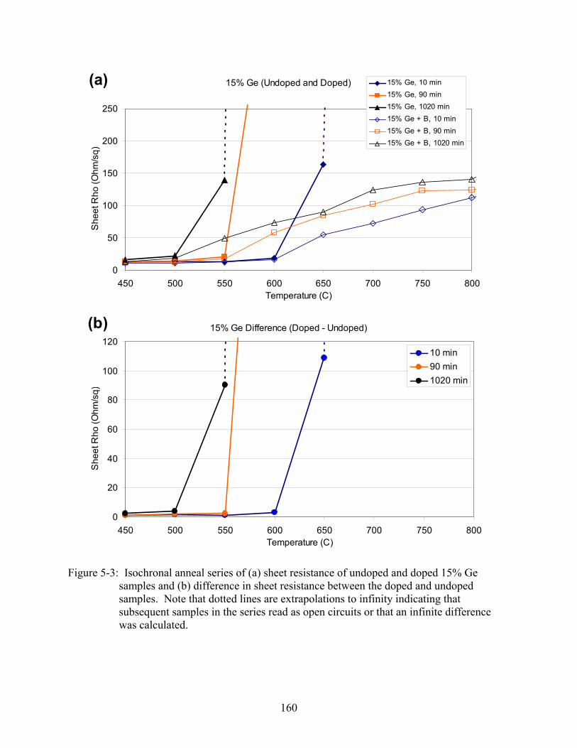
160
15% Ge (Undoped and Doped)
0
50
100
150
200
250
450 500 550 600 650 700 750 800Temperature (C)
She
et R
ho (O
hm/s
q)15% Ge, 10 min15% Ge, 90 min15% Ge, 1020 min15% Ge + B, 10 min15% Ge + B, 90 min15% Ge + B, 1020 min
15% Ge Difference (Doped - Undoped)
0
20
40
60
80
100
120
450 500 550 600 650 700 750 800Temperature (C)
She
et R
ho (O
hm/s
q)
10 min90 min1020 min
(b)
(a)
Figure 5-3: Isochronal anneal series of (a) sheet resistance of undoped and doped 15% Ge samples and (b) difference in sheet resistance between the doped and undoped samples. Note that dotted lines are extrapolations to infinity indicating that subsequent samples in the series read as open circuits or that an infinite difference was calculated.
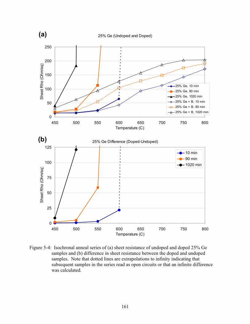
161
25% Ge (Undoped and Doped)
0
50
100
150
200
250
450 500 550 600 650 700 750 800Temperature (C)
She
et R
ho (O
hm/s
q)
25% Ge, 10 min25% Ge, 90 min25% Ge, 1020 min25% Ge + B, 10 min25% Ge + B, 90 min25% Ge + B, 1020 min
25% Ge Difference (Doped-Undoped)
0
25
50
75
100
125
450 500 550 600 650 700 750 800Temperature (C)
She
et R
ho (O
hm/s
q)
10 min90 min1020 min
(b)
(a)
Figure 5-4: Isochronal anneal series of (a) sheet resistance of undoped and doped 25% Ge samples and (b) difference in sheet resistance between the doped and undoped samples. Note that dotted lines are extrapolations to infinity indicating that subsequent samples in the series read as open circuits or that an infinite difference was calculated.

162
0
50
100
150
200
0.00 2000.00 4000.00 6000.00 8000.00 10000.00 12000.00Grain Size (arb units)
She
et R
esis
tanc
e (O
hm/s
q)15% Ge25% Ge15% Ge + B25% Ge + B
Figure 5-5: Plot of sample sheet resistance vs. Si1-zGez grain size.
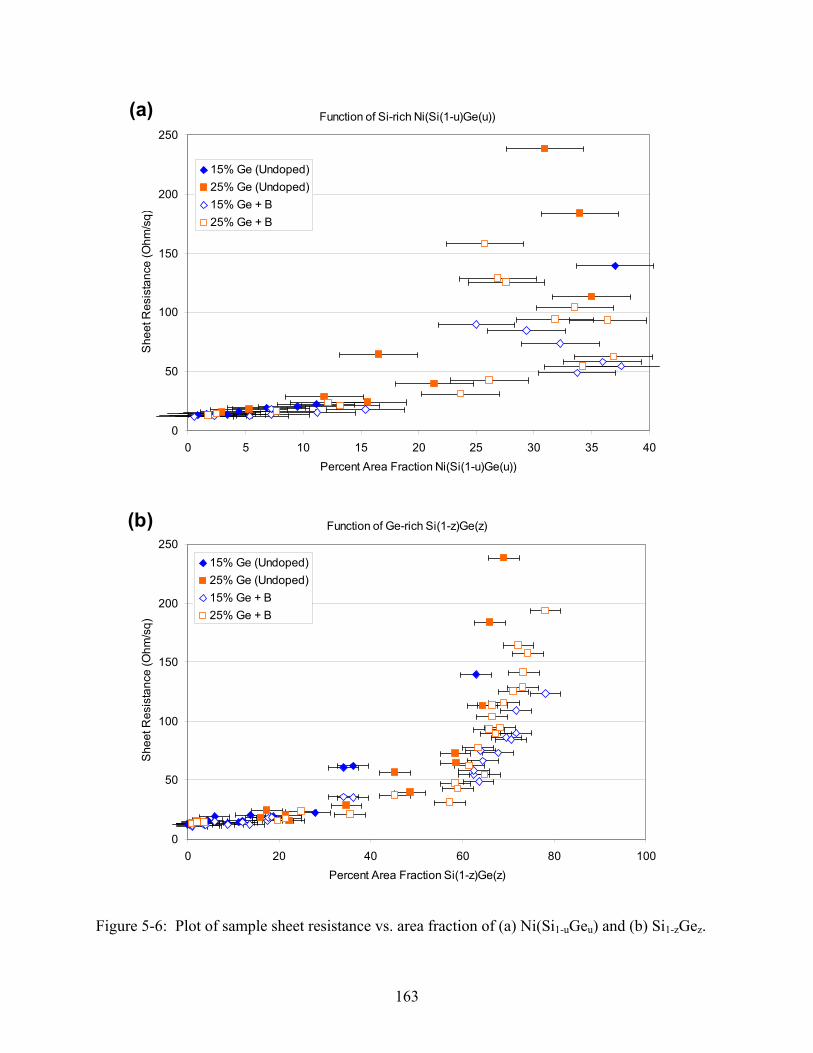
163
Function of Ge-rich Si(1-z)Ge(z)
0
50
100
150
200
250
0 20 40 60 80 100Percent Area Fraction Si(1-z)Ge(z)
She
et R
esis
tanc
e (O
hm/s
q)
15% Ge (Undoped)25% Ge (Undoped)15% Ge + B25% Ge + B
Function of Si-rich Ni(Si(1-u)Ge(u))
0
50
100
150
200
250
0 5 10 15 20 25 30 35 40Percent Area Fraction Ni(Si(1-u)Ge(u))
She
et R
esis
tanc
e (O
hm/s
q)
15% Ge (Undoped)25% Ge (Undoped)15% Ge + B25% Ge + B
(a)
(b)
Figure 5-6: Plot of sample sheet resistance vs. area fraction of (a) Ni(Si1-uGeu) and (b) Si1-zGez.
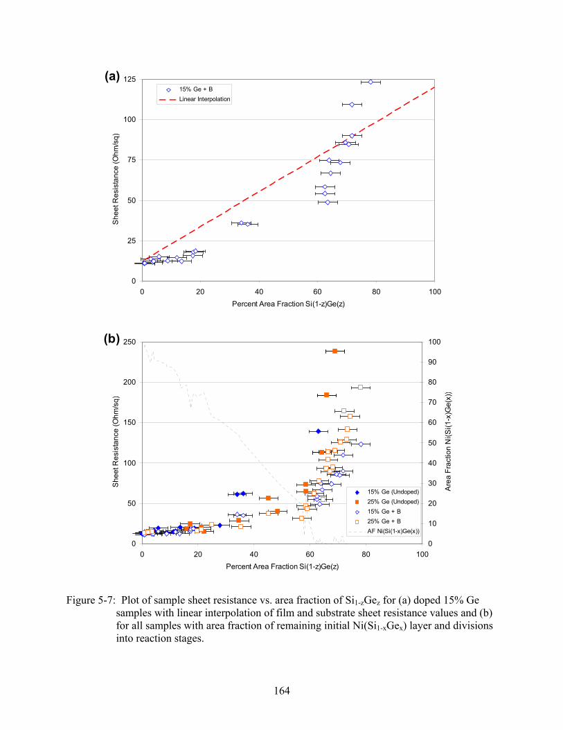
164
0
25
50
75
100
125
0 20 40 60 80 100Percent Area Fraction Si(1-z)Ge(z)
She
et R
esis
tanc
e (O
hm/s
q)
15% Ge + BLinear Interpolation
0
50
100
150
200
250
0 20 40 60 80 100Percent Area Fraction Si(1-z)Ge(z)
She
et R
esis
tanc
e (O
hm/s
q)
0
10
20
30
40
50
60
70
80
90
100
Are
a Fr
actio
n N
i(Si(1
-x)G
e(x)
)
15% Ge (Undoped)25% Ge (Undoped)15% Ge + B25% Ge + BAF Ni(Si(1-x)Ge(x))
(a)
(b)
Figure 5-7: Plot of sample sheet resistance vs. area fraction of Si1-zGez for (a) doped 15% Ge samples with linear interpolation of film and substrate sheet resistance values and (b) for all samples with area fraction of remaining initial Ni(Si1-xGex) layer and divisions into reaction stages.
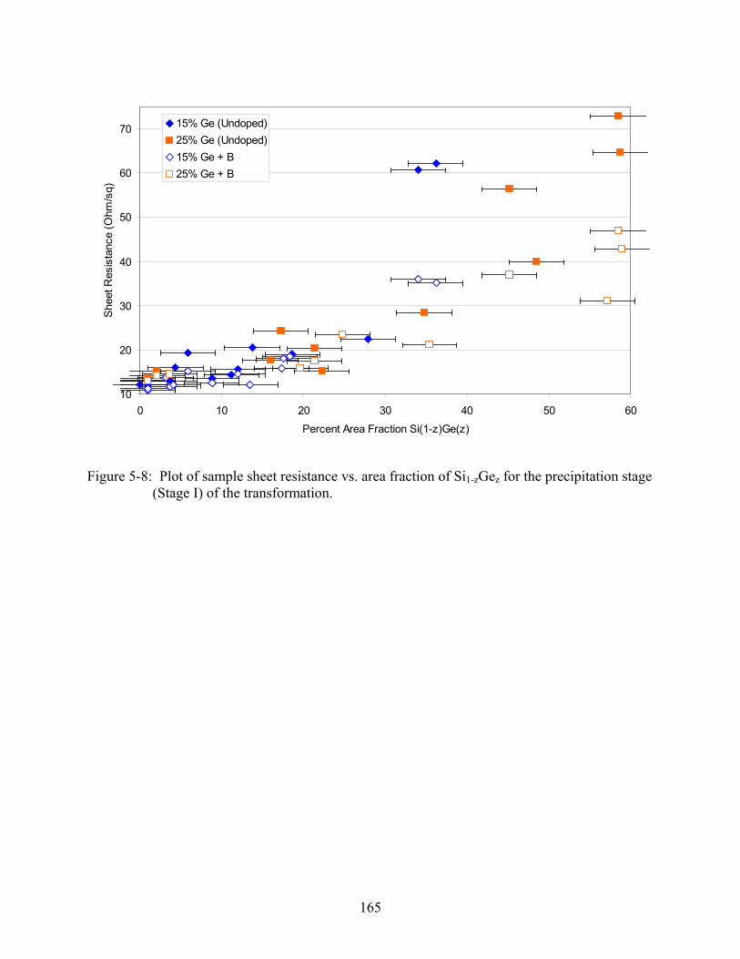
165
10
20
30
40
50
60
70
0 10 20 30 40 50 60
Percent Area Fraction Si(1-z)Ge(z)
She
et R
esis
tanc
e (O
hm/s
q)15% Ge (Undoped)25% Ge (Undoped)15% Ge + B25% Ge + B
Figure 5-8: Plot of sample sheet resistance vs. area fraction of Si1-zGez for the precipitation stage (Stage I) of the transformation.

166
Undoped
R2 = 0.7454
R2 = 0.8431
0
10
20
30
40
50
60
70
80
0 10 20 30 40 50 60Percent Area Fraction Si(1-z)Ge(z)
She
et R
esis
tanc
e (O
hm/s
q)15% Ge (Undoped)25% Ge (Undoped)
Doped
R2 = 0.8663
R2 = 0.8423
0
10
20
30
40
50
60
70
80
0 10 20 30 40 50 60Percent Area Fraction Si(1-z)Ge(z)
She
et R
esis
tanc
e (O
hm/s
q)
15% Ge + B25% Ge + B
(a)
(b)
Figure 5-9: Plot of Stage I sample sheet resistance vs. area fraction of Si1-zGez for (a) undoped and (b) doped samples. Best fit linear regression lines are also shown.

167
Regression Intercept
-5
0
5
10
15
20
Inte
rcep
t Val
ue
15% Ge (Undoped)
25% Ge (Undoped)
15% Ge + B
25% Ge + B
Regression Slope
0
0.25
0.5
0.75
1
1.25
1.5
1.75
Slo
pe V
alue
15% Ge (Undoped)
25% Ge (Undoped)
15% Ge + B
25% Ge + B
(a)
(b)
Figure 5-10: Plot of Stage I linear regression (a) intercept and (b) slope of the results given in Table 5-1. The 95% confidence interval for each value is also shown.
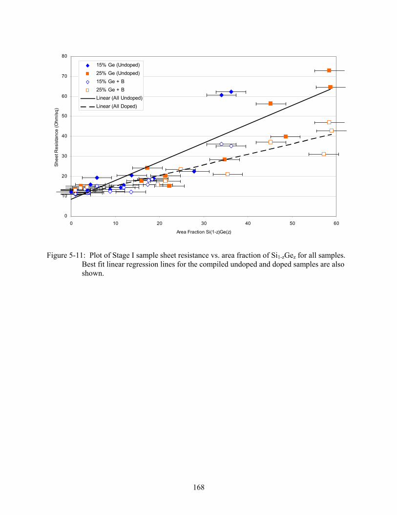
168
0
10
20
30
40
50
60
70
80
0 10 20 30 40 50 60
Area Fraction Si(1-z)Ge(z)
She
et R
esis
tanc
e (O
hm/s
q)
15% Ge (Undoped)25% Ge (Undoped)15% Ge + B25% Ge + BLinear (All Undoped)Linear (All Doped)
Figure 5-11: Plot of Stage I sample sheet resistance vs. area fraction of Si1-zGez for all samples. Best fit linear regression lines for the compiled undoped and doped samples are also shown.
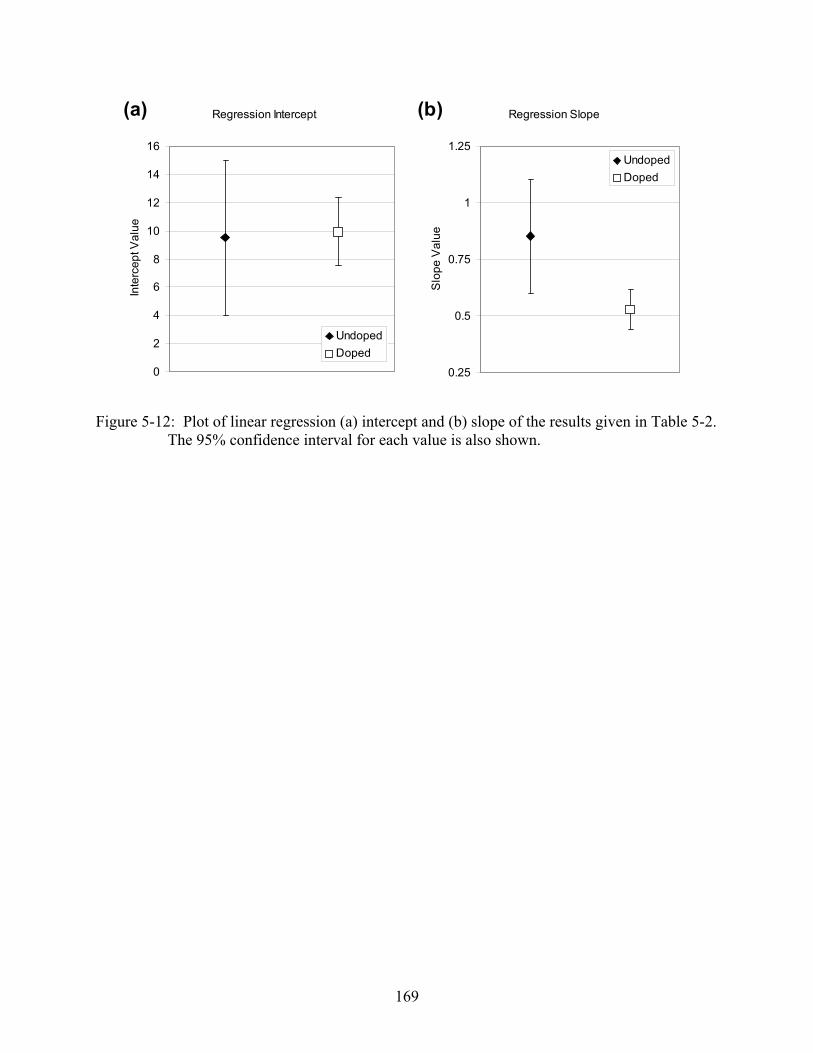
169
Regression Intercept
0
2
4
6
8
10
12
14
16In
terc
ept V
alue
UndopedDoped
Regression Slope
0.25
0.5
0.75
1
1.25
Slo
pe V
alue
UndopedDoped
(a) (b)
Figure 5-12: Plot of linear regression (a) intercept and (b) slope of the results given in Table 5-2.
The 95% confidence interval for each value is also shown.

170
(a)
(b)
Figure 5-13: Images of (a) raw SEM/BSE image for undoped 25% Ge sample annealed at 450 oC for 1020 minutes and (b) image of same sample after ImageJ processing and threshold application with example tortuosity calculation shown.

171
y = 0.0029x + 1.0149R2 = 0.9253
1
1.05
1.1
1.15
1.2
1.25
0 10 20 30 40 50 60 70
Area Fraction Si(1-z)Ge(z)
Tort
uosi
ty
25% Ge (Undoped)25% Ge + B
y = 0.0102e7.1279x
R2 = 0.8636 y = 0.0264e6.0707x
R2 = 0.8743
10
15
20
25
30
35
40
45
1 1.05 1.1 1.15 1.2 1.25Tortuosity
Shee
t Res
ista
ce (O
hm/s
q)
25% Ge (Undoped)25% Ge + BExpon. (25% Ge (Undoped))Expon. (25% Ge + B)
(a)
(b)
Figure 5-14: Plots of (a) conductive path tortuosity vs. area fraction Si1-zGez and (b) sample sheet resistance vs. tortuosity for selected undoped and doped 25% Ge samples. Best fit linear regression line for compiled undoped and doped samples is shown in (a).

172
Undoped
100
1000
10000
60 65 70 75 80Percent Area Fraction Si(1-z)Ge(z)
She
et R
esis
tanc
e (O
hm/s
q)15% Ge (Undoped)25% Ge (Undoped)
Doped
25
50
75
100
125
150
175
200
60 65 70 75 80Area Fraction Si(1-z)Ge(z)
She
et R
esis
tanc
e
15% Ge + B25% Ge + B
(a)
(b)
Figure 5-15: Sheet resistance of (a) undoped and (b) doped 15 and 25% Ge samples as a function of Si1-zGez area fraction for the agglomeration stage (Stage II) of the film transformation. Best fit linear regression lines for 15 and 25% Ge samples are shown in (b).

173
10
100
1000
10000
60 65 70 75 80Percent Area Fraction Si(1-z)Ge(z)
She
et R
esis
tanc
e (O
hm/s
q)
15% Ge (Undoped)25% Ge (Undoped)15% Ge + B25% Ge + B
Figure 5-16: Sheet resistance as a function of Si1-zGez area fraction for all samples in Stage II (agglomeration) of the film transformation.
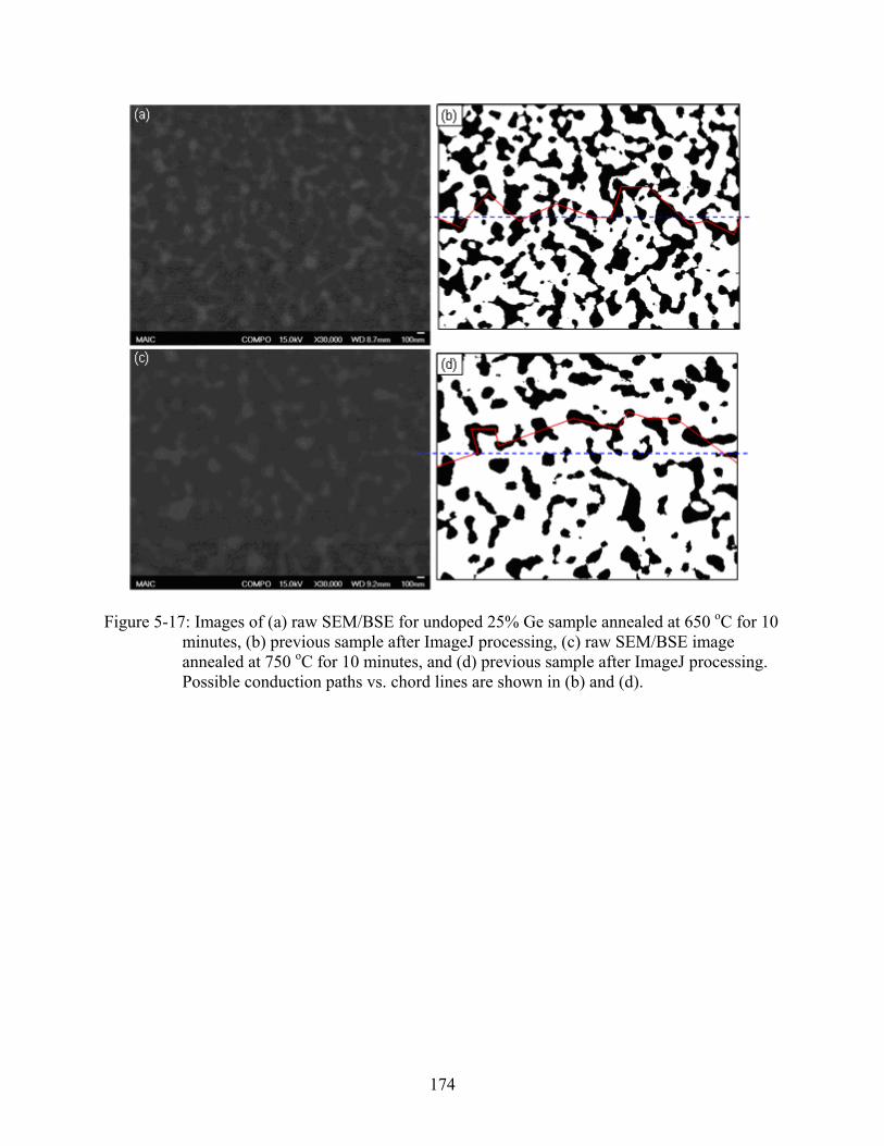
174
Figure 5-17: Images of (a) raw SEM/BSE for undoped 25% Ge sample annealed at 650 oC for 10 minutes, (b) previous sample after ImageJ processing, (c) raw SEM/BSE image annealed at 750 oC for 10 minutes, and (d) previous sample after ImageJ processing. Possible conduction paths vs. chord lines are shown in (b) and (d).
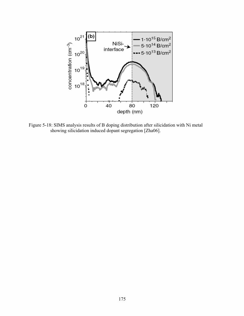
175
Figure 5-18: SIMS analysis results of B doping distribution after silicidation with Ni metal showing silicidation induced dopant segregation [Zha06].
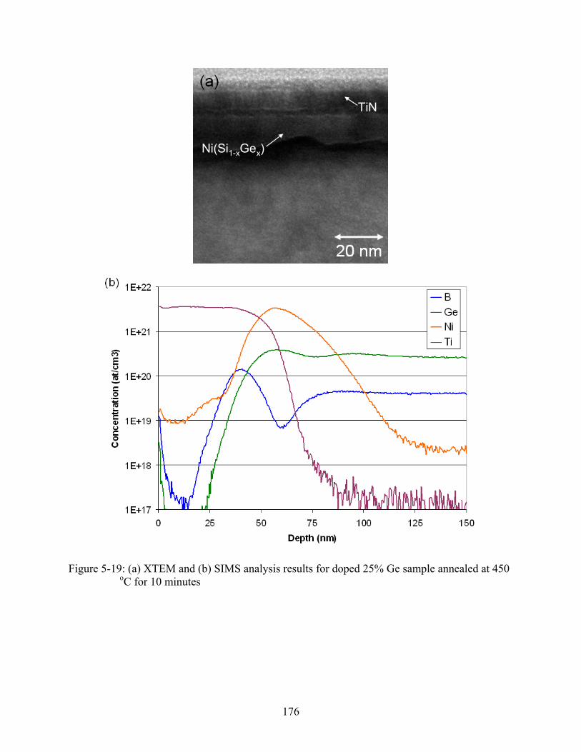
176
Ni(Si1-xGex)
TiN
Figure 5-19: (a) XTEM and (b) SIMS analysis results for doped 25% Ge sample annealed at 450 oC for 10 minutes
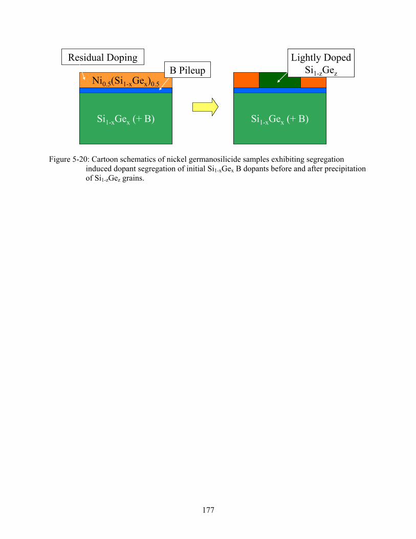
177
Si1-xGex (+ B)Si1-xGex (+ B)
Ni0.5(Si1-xGex)0.5
B Pileup
Si1-xGex (+ B)
Lightly Doped Si1-zGez
Si1-xGex (+ B)Si1-xGex (+ B)
Lightly Doped Si1-zGez
Residual Doping
Figure 5-20: Cartoon schematics of nickel germanosilicide samples exhibiting segregation induced dopant segregation of initial Si1-xGex B dopants before and after precipitation of Si1-zGez grains.

178
Sheet Resistance
0
25
50
75
100
125
150
450 500 550 600 650 700 750 800Temperature (C)
She
et R
esis
tanc
e (O
hm/s
q)
10 min
90 min
1020 min
Homogeneous NiSiGe
10 nm pileup and 120 nm ofSiGe + B in parallel130 nm SiGe + B (No Pileup)
Figure 5-21: Isochronal anneal series of doped 15% Ge samples with calculated sheet resistance
values for the potential alternative conduction paths.
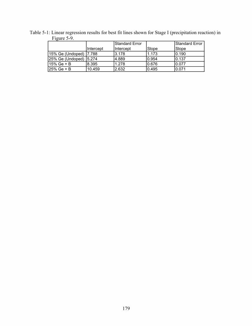
179
Table 5-1: Linear regression results for best fit lines shown for Stage I (precipitation reaction) in Figure 5-9.
InterceptStandard Error Intercept Slope
Standard Error Slope
15% Ge (Undoped) 7.788 3.178 1.173 0.19025% Ge (Undoped) 5.274 4.889 0.954 0.13715% Ge + B 8.395 1.278 0.676 0.07725% Ge + B 10.459 2.632 0.495 0.071
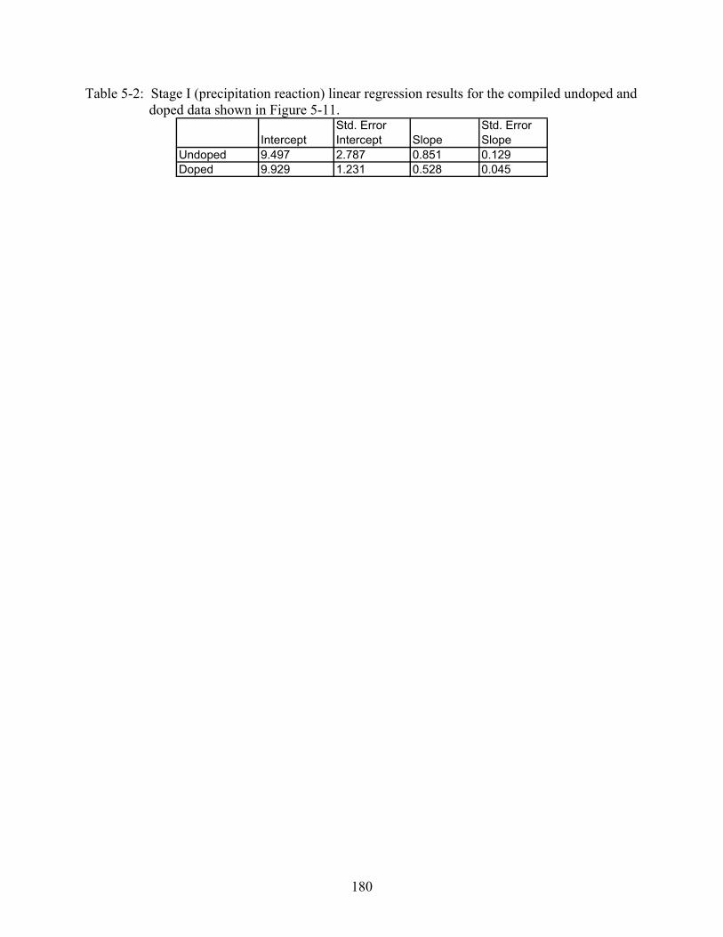
180
Table 5-2: Stage I (precipitation reaction) linear regression results for the compiled undoped and doped data shown in Figure 5-11.
InterceptStd. Error Intercept Slope
Std. Error Slope
Undoped 9.497 2.787 0.851 0.129Doped 9.929 1.231 0.528 0.045

181
Table 5-3: Measurements of Si1-zGez area fraction, tortuosity, and sheet resistance for selected undoped and doped 25% Ge samples.
Temperature (C) Time (min) % AF
Si(1-z)Ge(z) TortuositySheet Resistance (Ohm/sq)
15% Ge (Undoped) 450 30 2.10 1.010 15.1415% Ge (Undoped) 450 90 15.95 1.080 17.6915% Ge (Undoped) 450 1020 48.50 1.150 39.8515% Ge (Undoped) 500 30 21.33 1.070 20.3515% Ge (Undoped) 500 90 34.73 1.100 28.3925% Ge (Undoped) 450 90 19.60 1.083 15.7925% Ge (Undoped) 450 1020 57.15 1.160 31.1925% Ge (Undoped) 500 10 3.63 1.016 14.5325% Ge (Undoped) 550 10 35.40 1.120 21.0825% Ge (Undoped) 550 30 45.17 1.172 37.00
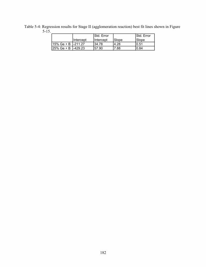
182
Table 5-4: Regression results for Stage II (agglomeration reaction) best fit lines shown in Figure 5-15.
InterceptStd. Error Intercept Slope
Std. Error Slope
15% Ge + B -211.27 34.78 4.28 0.5125% Ge + B -429.23 57.90 7.88 0.84

183
CHAPTER 6 CONCLUSIONS AND FUTURE WORK
The stated objective of this work was to clarify certain outstanding issues regarding the
morphological stability and electronic properties of nickel germanosilicide thin films. The
following sections discuss the results and conclusions determined by this work in the context of
these outstanding issues. A discussion of potential future work which would complement the
results of this work is also included.
6.1 Conclusions
Three major research objectives were addressed by the experimentation in this work. The
three objectives included clarification and quantification of the structure/property relationship
which published literature had proposed to exist between nickel germanosilicide film
agglomeration and increases in film sheet resistance, further investigation of the influence of
high levels of homogeneous B doping on the relationship, and expansion of the thermal matrix in
which films were studied in order to gain information about the kinetics of the agglomeration
process. The following sections discuss the findings of the experiments performed in this work
in terms of these three objectives.
6.1.1 Microstructure and Kinetics
Prior studies available in literature have utilized isochronal experiments with very short
annealing times (30 to 60 seconds). This work aimed to expand the knowledge of the behavior
of nickel germanosilicide films over a much larger range of anneal times and temperatures,
including both isochronal and isothermal series. Through analysis of samples annealed at
temperatures ranging from 450 to 800 oC and times from 10 minutes to 1020 minutes,
information about the kinetics of the phase transformation was obtained.
184
Results from the analysis of the annealed samples showed that the general cross-section
and plan-view morphology of the nickel germanosilicide films in this work agreed well with
those reported in prior literature. Also, while prior work has generally described the film
evolution as �“agglomeration,�” two distinct reactions were captured by the anneal matrix used in
this work. Initially, Ge-rich Si1-zGez grains precipitated from the parent film as Ge was rejected
(presumably to the grain boundaries). This process continued until the parent film had
completely transformed in to Ge-rich Si1-zGez and Si-rich Ni(Si1-uGeu) grains. Complete
transformation corresponded to ~60% area fraction Ge-rich Si1-zGez for all samples in this work.
Once the transformation was complete, the Si-rich Ni(Si1-uGeu) grains then began to
agglomerate. It was also shown that increasing Ge content in the initial Si1-xGex film from 15 to
25% increased the amount of transformation observed for equivalent anneals, likely due to the
increase in driving force for Ge rejection with increasing Ge content.
It was also determined that the reaction kinetics for both stages of the film transformation
could be modeled using general Avrami isothermal transformation curves. Two separate
reaction orders were observed, corresponding to the precipitation and agglomeration reactions.
By analysis of the reaction order, the precipitation reaction was determined to be diffusion
controlled growth with a zero nucleation rate. The agglomeration reaction was similarly
determined to be diffusion controlled thickening of very large plates. The activation energies of
the reactions were also able to be calculated and showed that for the precipitation reaction, Ea
was 1.96 and 0.76 eV for the 15 and 25% Ge samples, respectively. For the agglomeration
reaction, Ea was determined to be 0.14 and 0.10 eV, respectively (though statistically these
values were found to be equal).
185
6.1.2 Structure/Property Relationship
Prior literature has proposed a qualitative link between the agglomeration of a nickel
germanosilicide thin film and increases in the film�’s sheet resistance. The evidence in favor of
the relationship, however, was circumstantial and no quantitative relationship had been
established. Therefore, one objective this work was to clarify the relationship by determining if
a direct, quantitative relationship could be established between a metric describing film
agglomeration and sheet resistance. The influence of increasing Ge content was on the
structure/property relationship was also studied.
The best metric for establishing a structure/property relationship between the film quality
and its sheet resistance was determined to be the area fraction of Ge-rich Si1-zGez present in the
film. Use of this metric allowed a direct, quantitative relationship to be established in both the
precipitation and agglomeration stages of the film transformation. For the precipitation stage of
the transformation, the sheet resistance was found to increase linearly with increasing area
fraction of Si1-zGez. Increasing Ge content in this stage of the reaction did not affect the
relationship. It was determined, therefore, that the influence of increasing Ge on sheet resistance
could be attributed solely to the increased agglomeration seen in these samples and not to a
fundamental change in the structure/property relationship. Overall, the general increase in sheet
resistance for all samples in this stage of the transformation was found to be attributable to the
increasing tortuosity of the conduction path with increasing Si1-zGez precipitation. For the
agglomeration stage of the film transformation, the sheet resistance of the undoped samples was
found to rapidly increase to large (or infinite) values unrelated to the amount of Si1-zGez present
and no quantitative structure/property was able to be established. The influence of Ge content
was similarly unable to be determined. This effect was determined to be due to the absence of a
continuous conduction path between isolated Si-rich Ni(Si1-uGeu) grains for these sample. The
186
doped samples, however, showed a linear trend of increasing sheet resistance with increasing
area fraction Si1-zGez, though with a greater slope than seen in the precipitation stage of the
reaction.
6.1.3 Influence of Homogeneous B Doping
Prior literature has proposed that high levels of homogeneous B doping in the initial Si1-
xGex layer can suppress the agglomeration process and thus stabilize sheet resistance. The prior
work, however, did not utilize direct measurement techniques when evaluating film
agglomeration and so the degree of suppression, if any, is not well quantified. Accordingly, this
work aimed to confirm the presence of agglomeration suppression using plan-view SEM
imaging. This work also aimed to determine if the quantitative relationship between
agglomeration and sheet resistance was maintained for B doped samples.
Analysis of the samples in this work showed that the addition of ~4.5E19 atoms/cm2
homogeneous B doping during Si1-xGex layer growth did not affect the morphology of the nickel
germanosilicide film microstructure for any anneal time or temperature. The doped samples,
however, showed a decrease and stabilization of sheet resistance values for both the 15 and 25%
Ge samples used in this work in accordance with prior literature. This effect was determined to
be present in both the precipitation and agglomeration stages of the film transformation, though
the magnitude of the effect was much larger in the latter stage. Overall, these results suggested
that a mechanism other than a decrease in agglomeration, most likely an alternative conduction
path in the B doped structures, was responsible for the effects. This path was also determined to
most likely be the unreacted, nominally B doped Si1-xGex layer below the nickel germanosilicide
layer. This conclusion also suggested that differences in the sheet resistance of the Si1-xGex layer
with changing Ge content, though unconfirmed, caused the difference in structure/property
relationship for the doped samples within the agglomeration stage of the transformation.
187
6.2 Future Work
While this work clarified many of the outstanding questions concerning the stability and
behavior of nickel germanosilicide thin films, some questions were also raised by this work.
Specifically, the cause for the increase of activation energy for the precipitation reaction with
increasing Ge content is not known. Also, the existence of segregation induced dopant
segregation was not directly observed for the samples in this work, nor was the distributions of
the B dopant determined within the structure for each anneal time and temperature. These points
could possibly be clarified by performing additional investigations of the nickel germanosilicide
system using Local Electrode Atom Probe (LEAP) analysis.
LEAP analysis has been shown to be able to provide three dimensional maps of atomic
distributions for semiconducting samples [Kel04,]. The technique has also been shown to be
sensitive enough to investigate the lateral distribution of a gate structure implanted with B dopant
[Moo08]. It is expected, therefore, that LEAP analysis of samples similar to those used in this
work could provide information about B and Ge distributions in proximity to the grain
boundaries of the germanosilicide grains. With such information, the mechanism by which Ge is
rejected from the sample (i.e. via bulk or grain boundary diffusion) could possibly be clarified.
The cause for the concentration dependence of the activation energy might, in turn, also be
clarified. The B dopant distribution, specifically confirmation of whether silicidation induced
dopant segregation is present, could definitely be determined through LEAP analysis.
Information about the doping of the precipitated Si1-zGez grains could also be determined through
this type of analysis. This information would, in turn, allow confirmation of the alternative
conduction path for the B doped samples.
Another area of potential future research would be the continued investigation of the
relationship between area fraction of precipitated Si1-zGez, conduction path tortuosity, and

188
sample sheet resistance. The tortuosity investigations in this work were performed using manual
measurement and calculations. It is expected, therefore, if computer software was used to
measure tortuosity measurement error would decrease. The more rapid speed of software-based
calculations would also allow both a larger number of samples at each anneal time and
temperature to be studied as well as a larger overall number of anneal times and temperatures.
Additionally, software aided analysis may allow the modeling of the conductive path for the
doped samples in the agglomeration stage of the relationship to explain the linear dependence of
sheet resistance on area fraction of Si1-zGez. Both of these analyses will require higher
resolution, less noisy SEM images of the samples, as the graininess of the images (and the
resulting difficulty of defining the grain edges) was the primary reason such analyses were not
attempted in this work.
Performing these additional investigations would continue to develop the scientific
knowledge of the behavior of nickel germanosilicide thin films. This knowledge, in turn, can
then be used to address the use of such films as intermediate layers between semiconductor
devices and metallization layers.
189
APPENDIX A ERROR IN SEM/BSE IMAGE QUANTIFICATION
SEM/BSE images in this work were mainly quantified using ImageJ software. To validate
the repeatability of the SEM/BSE image quantification in this work, as well as explore the
repeatability of the anneal process and regional sample variation, samples of the undoped, 15%
Ge samples were annealed at 550 oC for 90 minutes on three separate occasions. Between each
anneal, the furnace was set to another temperature and then re-set back to 550 oC. While it does
not represent an exact center point in the experimental matrix, the data point (undoped, 15% Ge,
550 oC, 90 minute) selected for replication was chosen as it displays the most complex
intermediate morphology with all three phases, Ni(Si1-xGex), Ni-rich Ni(Si1-uGeu), and Ge-rich
Si1-zGez, present in the image. It is expected, therefore, that the variation in this sample would be
the highest in the experiment due to the difficulty in quantizing the complex microstructure. By
applying the variation found at this data point to the entire matrix, a conservative estimate of
variation would be included in the data analysis. Additional data points for replication were not
chosen due to time and resource constraints.
Once annealed, each of the replicates was imaged at 30,000x magnification using
SEM/BSE five times in two separate regions on each sample, for a grand total of 30 images.
This nested design allowed both sample-to-sample and region-to-region comparisons to be made.
The area fraction of Ni-rich Ni(Si1-uGeu) and Ge-rich Si1-zGez phases present in each image was
then quantified using ImageJ and the results analyzed with Minitab to determine the variation in
the process.
Individual value plots of the area fraction values divided by sample and region are shown
in Figure A-1 for both response variables. The plots indicate the qualitative presence of some
variation, both between and within each sample. To determine if the apparent variation was
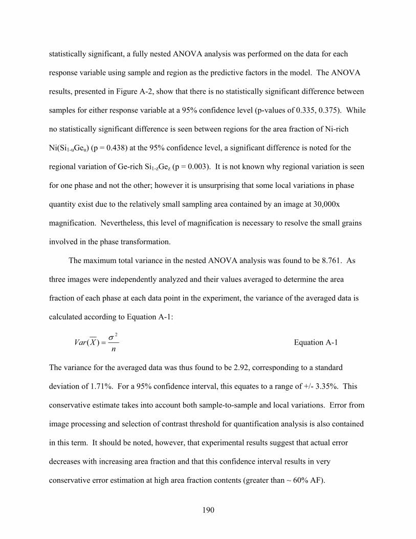
190
statistically significant, a fully nested ANOVA analysis was performed on the data for each
response variable using sample and region as the predictive factors in the model. The ANOVA
results, presented in Figure A-2, show that there is no statistically significant difference between
samples for either response variable at a 95% confidence level (p-values of 0.335, 0.375). While
no statistically significant difference is seen between regions for the area fraction of Ni-rich
Ni(Si1-uGeu) (p = 0.438) at the 95% confidence level, a significant difference is noted for the
regional variation of Ge-rich Si1-zGez (p = 0.003). It is not known why regional variation is seen
for one phase and not the other; however it is unsurprising that some local variations in phase
quantity exist due to the relatively small sampling area contained by an image at 30,000x
magnification. Nevertheless, this level of magnification is necessary to resolve the small grains
involved in the phase transformation.
The maximum total variance in the nested ANOVA analysis was found to be 8.761. As
three images were independently analyzed and their values averaged to determine the area
fraction of each phase at each data point in the experiment, the variance of the averaged data is
calculated according to Equation A-1:
n
XVar2
)( Equation A-1
The variance for the averaged data was thus found to be 2.92, corresponding to a standard
deviation of 1.71%. For a 95% confidence interval, this equates to a range of +/- 3.35%. This
conservative estimate takes into account both sample-to-sample and local variations. Error from
image processing and selection of contrast threshold for quantification analysis is also contained
in this term. It should be noted, however, that experimental results suggest that actual error
decreases with increasing area fraction and that this confidence interval results in very
conservative error estimation at high area fraction contents (greater than ~ 60% AF).
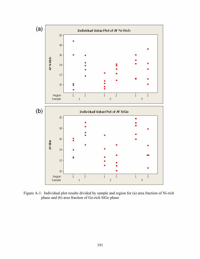
191
Figure A-1: Individual plot results divided by sample and region for (a) area fraction of Ni-rich phase and (b) area fraction of Ge-rich SiGe phase
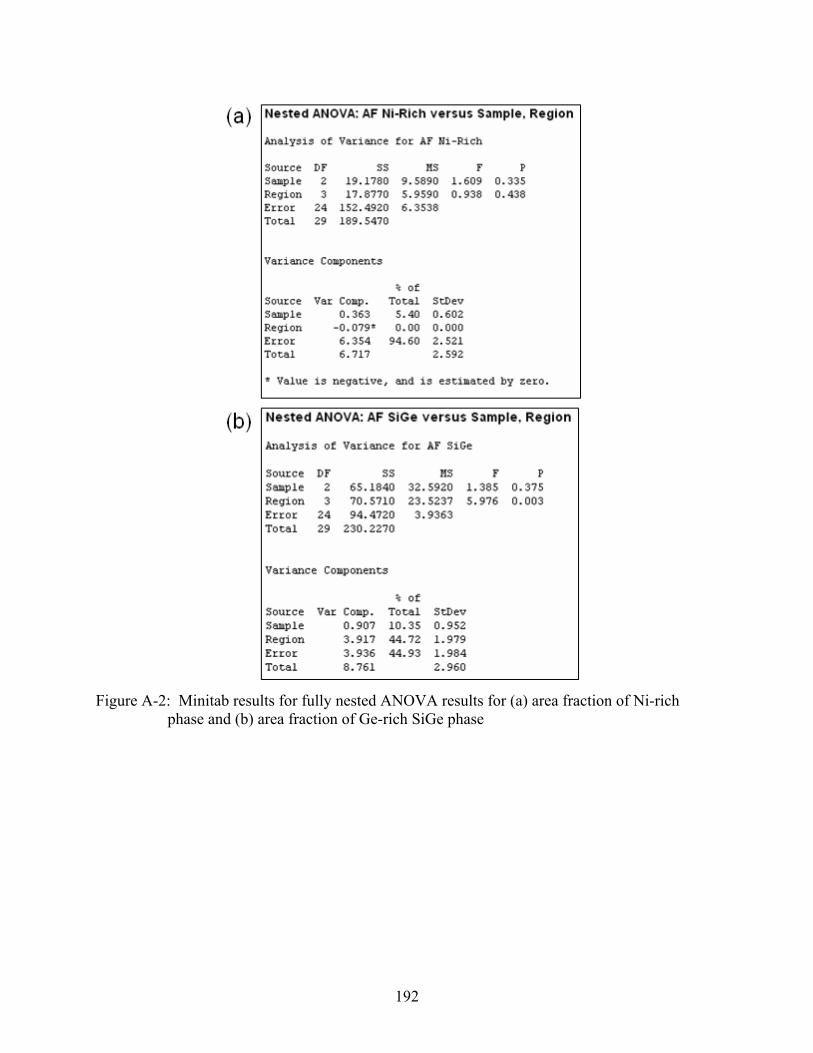
192
Figure A-2: Minitab results for fully nested ANOVA results for (a) area fraction of Ni-rich
phase and (b) area fraction of Ge-rich SiGe phase
193
APPENDIX B GAUGE REPEATABILITY AND REPRODUCIBILITY ANALYSIS OF 4PP
MEASUREMENT
A full gauge repeatability and reproducibility study (gauge R&R) was performed on the
four point probe (4PP) sheet resistance measurement technique used in this work. For this study,
10 samples were selected at random from the full anneal matrix used in this work. Three
operators then measured the sheet resistance of each sample in random order. This process was
then repeated twice (with the order of the samples randomly re-arranged between each
repetition) for a total of 3 repetitions and a grand total of 90 measurements.
Of the three operators, only one operator (the author of this work) was able to successfully
measure every sample for each of the three repetitions. In total, only 5 of the 10 samples were
successfully measured for all repetitions by all operators. For the five samples that were not
completely successfully measured, some samples were successfully analyzed by an operator for
none, one, or two repetitions. These results indicate problems with both the repeatability and
reproducibility of the measurement process.
Data from the five samples that were completely successfully measured was analyzed
using a Gauge R&R ANOVA package contained in the Minitab 15.1.1.0 software. The results,
presented in Figure B-1, indicate very low contributions to the total study deviation by both
measurement repeatability and reproducibility. These results are very interesting when taken in
conjunction with the fact that many samples could not be successfully measured by some
operators. Thus, it can be concluded that while an operator may have a difficult time obtaining a
successful measurement of a sample, if a measurement is obtained it is of good quality.
While this finding is of general interest regarding the measurement process, all sheet
resistance measurements presented in this work were taken by a single operator (the author).
Hence, a deeper understanding of the repeatability of the measurement process by this operator is
194
of interest when analyzing the results in this work. Accordingly, a one-way ANOVA analysis
was performed on the results from this operator. As this operator successfully obtained
measurements for all samples in the study, data from all 10 samples was used in the analysis.
The ANOVA results from this analysis, presented in Figure B-2, indicate that both repeatability
and part-to-part variation contribute to the total overall variance in the study. It can also be
observed in the results that one sample, number 9, has a sheet resistance several orders of
magnitude higher than the other samples in the study. It is also apparent that the sheet resistance
measurements of this sample varied over a considerable range (from ~2000 to ~6500 Ohm/sq).
This observation suggests that measurement repeatability may suffer for samples with very high
sheet resistances. To further explore this supposition, the data from sample 9 was eliminated
from the study and the ANOVA analysis performed again. The results from the revised analysis
are presented in Figure B-3 and show that the contribution of repeatability to the study variation
has decreased to less than 5% of the overall value. It can be concluded, therefore, that the sheet
resistance measurement process is repeatable for this operator (the author) for most samples. If a
sample presents a very high sheet resistance value (on the order of thousands of Ohm/sq),
however, it should be cautioned that significant variation in the results may be present.
Nevertheless, most samples in this work have sheet resistance values below ~200 Ohm/sq. For
these samples, based on the results from the revised ANOVA analysis of the first operator (the
author of this work), a 95% confidence interval of +/- 2.19 Ohm/sq can be applied to capture any
variation in the measurement process.
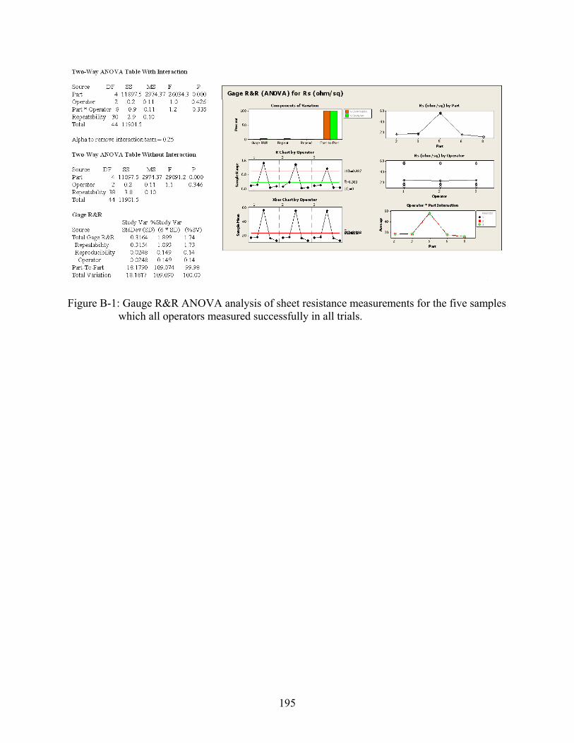
195
Figure B-1: Gauge R&R ANOVA analysis of sheet resistance measurements for the five samples which all operators measured successfully in all trials.
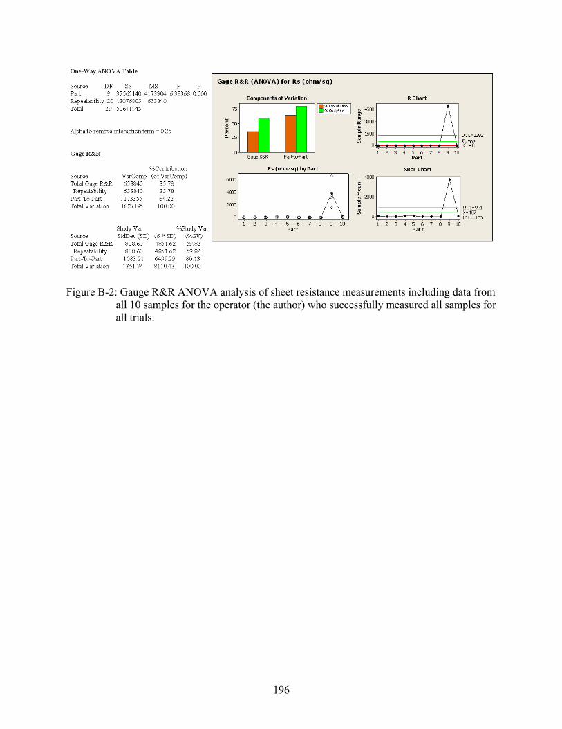
196
Figure B-2: Gauge R&R ANOVA analysis of sheet resistance measurements including data from all 10 samples for the operator (the author) who successfully measured all samples for all trials.
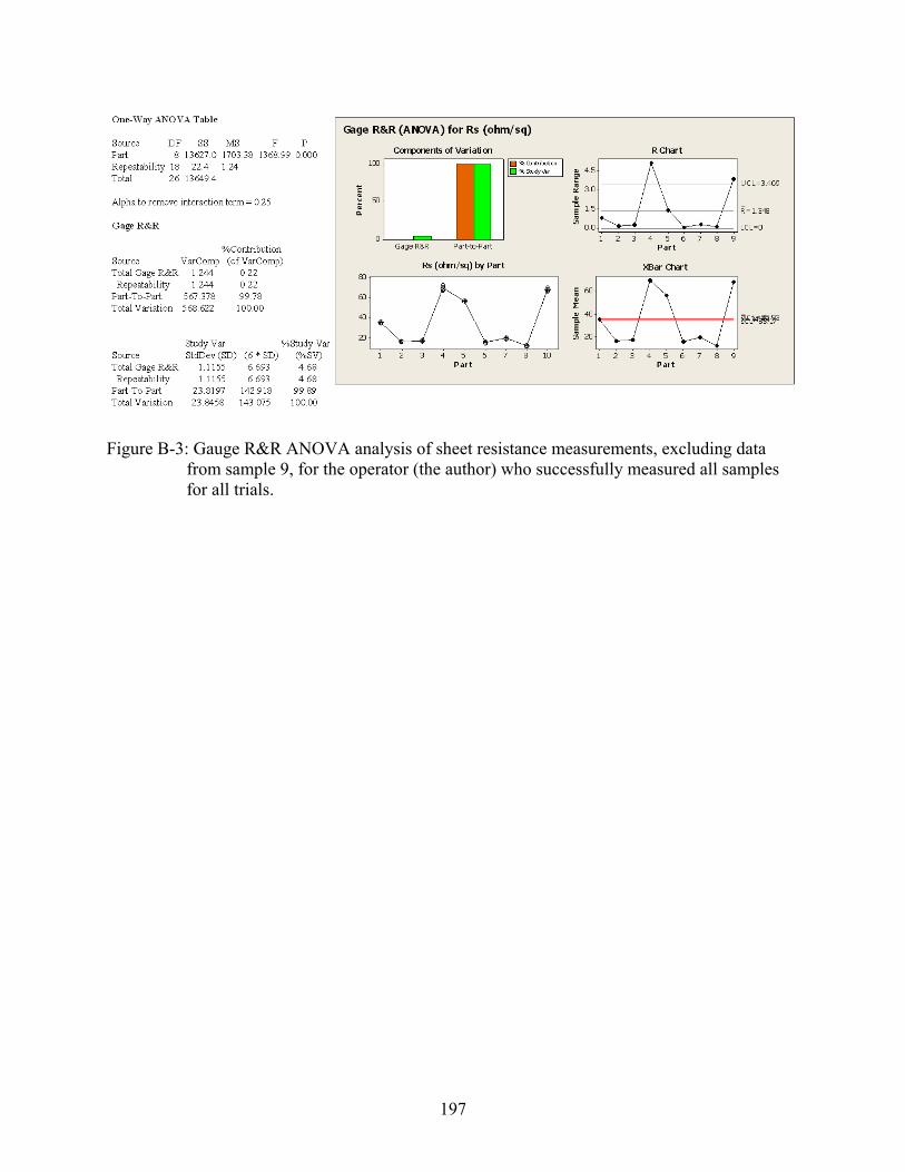
197
Figure B-3: Gauge R&R ANOVA analysis of sheet resistance measurements, excluding data from sample 9, for the operator (the author) who successfully measured all samples for all trials.
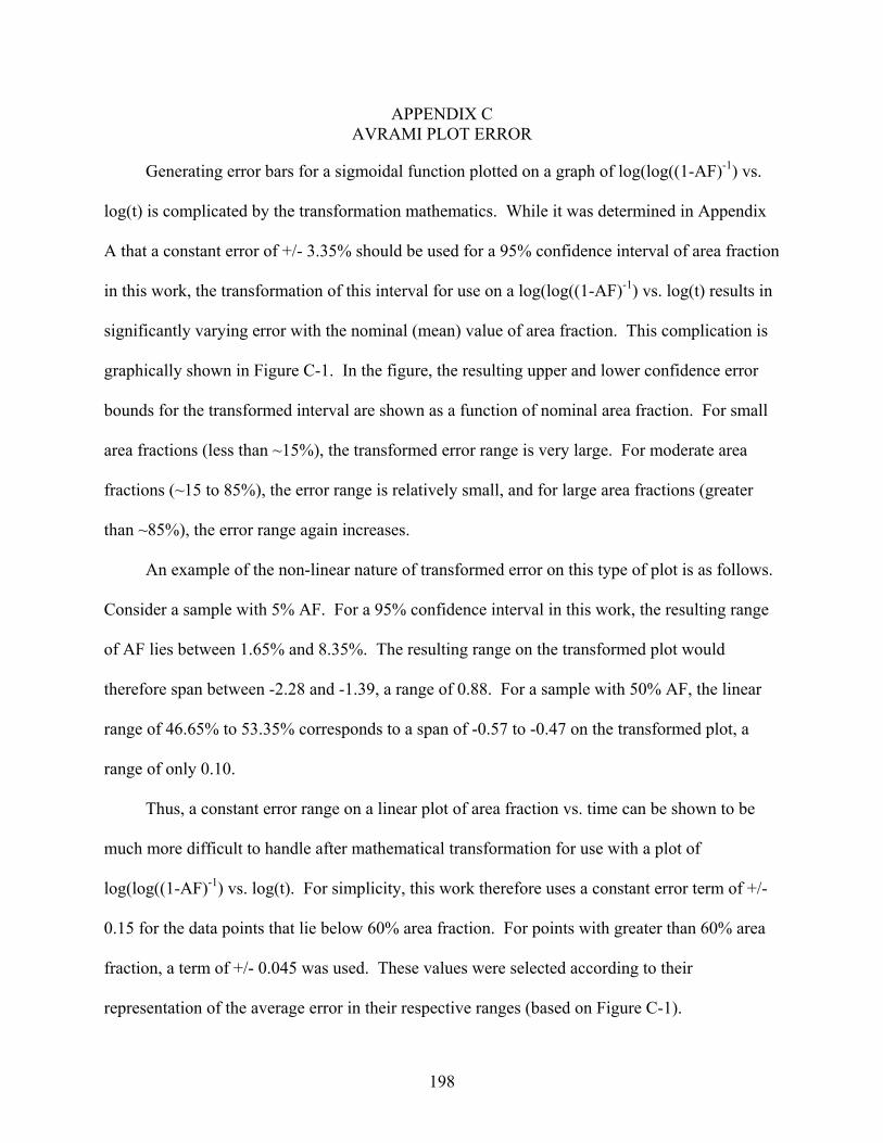
198
APPENDIX C AVRAMI PLOT ERROR
Generating error bars for a sigmoidal function plotted on a graph of log(log((1-AF)-1) vs.
log(t) is complicated by the transformation mathematics. While it was determined in Appendix
A that a constant error of +/- 3.35% should be used for a 95% confidence interval of area fraction
in this work, the transformation of this interval for use on a log(log((1-AF)-1) vs. log(t) results in
significantly varying error with the nominal (mean) value of area fraction. This complication is
graphically shown in Figure C-1. In the figure, the resulting upper and lower confidence error
bounds for the transformed interval are shown as a function of nominal area fraction. For small
area fractions (less than ~15%), the transformed error range is very large. For moderate area
fractions (~15 to 85%), the error range is relatively small, and for large area fractions (greater
than ~85%), the error range again increases.
An example of the non-linear nature of transformed error on this type of plot is as follows.
Consider a sample with 5% AF. For a 95% confidence interval in this work, the resulting range
of AF lies between 1.65% and 8.35%. The resulting range on the transformed plot would
therefore span between -2.28 and -1.39, a range of 0.88. For a sample with 50% AF, the linear
range of 46.65% to 53.35% corresponds to a span of -0.57 to -0.47 on the transformed plot, a
range of only 0.10.
Thus, a constant error range on a linear plot of area fraction vs. time can be shown to be
much more difficult to handle after mathematical transformation for use with a plot of
log(log((1-AF)-1) vs. log(t). For simplicity, this work therefore uses a constant error term of +/-
0.15 for the data points that lie below 60% area fraction. For points with greater than 60% area
fraction, a term of +/- 0.045 was used. These values were selected according to their
representation of the average error in their respective ranges (based on Figure C-1).

199
Error Range ( +/- 3.35% AF)
-3
-2.5
-2
-1.5
-1
-0.5
0
0.5
1
0 10 20 30 40 50 60 70 80 90 100
Area Fraction (%)
log(
log(
1/(1
-AF)
))
High Limit (+ 3.35%)NominalLow Limit (- 3.35%)
Figure C-1: Transformed error range for a constant +/- 3.35% range of area fraction as a function of nominal area fraction.

200
LIST OF REFERENCES
[Aub05] V. Aubry-Fortuna, P. Dollfus, S. Galdin-Retailleau, Solid-State Electron. 49, 1320 (2005)
[Avr39] M. Avrami, J. Chem. Phys. 7, 1103 (1939)
[Avr40] M. Avrami, J. Chem. Phys. 8, 212 (1940)
[Avr41] M. Avrami, J. Chem. Phys. 9, 177 (1941)
[Bai04] P. Bai et al., IEDM Tech. Dig. 2004, 657 (2004)
[Bar87] J.C. Barbour, A.E.M.J. Fischer, J.F. van der Veen, J. Appl. Phys. 62, 2582 (1987)
[Cha04] O. Chamirian, A. Lauwers, J.A. Kittl, M. Van Dal, M. De Potter, R. Lindsay, K. Maex, Mic. Eng. 76, 297 (2004)
[Cha04b] S. Chattopadhyay, L.D. Driscoll, K.S.K. Kwa, S.H. Olsen, A.G. O�’Neill, Solid State Electron. 48 1407 (2004)
[Che97] J. Chen, J.P. Colinge, D. Flandre, R. Gillon, J.P. Raskin, D. Vanhoenacker, J. Electrochem. Soc. 144(7), 2437 (1997)
[Chi04] P.R. Chidambaram, B.A. Smith, L.H. Hall, H. Bu, S. Chakravarthi, Y. Kimm VLSI Symp. Tech. Dig. Honolulu, HI, 48 (2004)
[Cho06a] Saurabh Chopra, Mehmet C. Ozturk, Veena Musra, Kris McGuire, Laurie E. McNeil, App. Phy. Lett. 88, 202114 (2006)
[Cho06b] Saurabh Chopra, Mehmet C. Ozturk, Veena Musra, Kris McGuire, Laurie E. McNeil, App. Phy. Lett. 89, 202118 (2006)
[Chr02] J.W. Christian, The Theory of Transformations in Metals and Alloys, Part I, Pergamon, Oxford (2002)
[Cro03] R.T. Crosby et al., Mat. Sci. in Semicond. Proc. 6, 205 (2003)
[dHe82] F. d�’Heurle, C.S. Petersson, L. Stolt, B. Stritzker, J. Appl. Phys. 53, 5678 (1982)
[dHe84] F.M. d�’Heurle, C.S. Petersson, J.E.E. Baglin, S.J. LaPlaca, C. Wong, J. Appl. Phys. 55, 4208 (1984)
[dHe89] F.M. d�’Heurle, J. Vac. Sci. Technol. A 7, 1467 (1989)
[dHe86] F.M. d�’Heurle P. Gas, J. Mater. Res., 1(1), 205 (1986)
[Dis54] J.P. Dismukes, L. Ekstrom, R.J. Paff, J. Phys. Chem. 68(10), 3021 (1964)

201
[Fin81] T.G. Finstad, Phys. Status Solidi. 63(a), 223 (1981)
[Gam98] J.P. Gambino, E.G. Colgan, Mat. Chem. Phys. 52, 99 (1998)
[Gan93] E. Ganin, S. Wind, P. Ronshei, A. Yapsir, K. Barmak, J. Bucchingnano, R. Assenz, Rapid Thermal and Integrated Processing II, Vol. 303, Materials Research Soc. Puttsburgh, PA, 109 (1993)
[Gan00] S. Gannavaram, N. Pesovic, M.C. Ozturk, in: Proceedings of the IEDM 2000, p.347 (2000)
[Gas98] P. Gas, F. d�’Heurle, Numerical Data and Functional relationships in Science and Technology Volume III, Landolt-Bornstein, Berlin 33A (1998)
[Ger04] P. Gergaud, C. Rivero, M. Gaillanou, O. Thomas, B. Froment, H. Jaouen, Mater. Sci. Eng. B 114-115, 67 (2004)
[He05] J.H. He, W.W. Wu, L.J. Chen, Nuc. Ins. Meth. Phys. Resch. B 237, 174 (2005)
[Hel97a] P.E. Hellberg, S.L. Zhang, C.S. Peterson, IEEE Elec. Dev. Lett. 18(9), 456 (1997)
[Hel97b] P. E. Hellberg, A. Gagnor, S.L. Zhang, C.S. Peterson, J. Electrochem. Soc. 144, 3968 (1997)
[Hsi88] Y.F. Hsieh, L.J. Chen, E.D. Marshall, S.S. Lau, Thin Solid Films 162, 287 (1988)
[Hua95] F.Y. Huang, X. Zhu, M.O. Tanner, K.L. Wang, Appl. Phys. Lett. 67(4), 566 (1995)
[Ish03] C. Isheden, J. Seger, H. Radamson, S.L. Zhang, M. Ostling, Mater. Res. Soc. Symp. Proc. 745, N4.9 (2003)
[Iwa85] M. Iwami, A. Hiraki, Jpn. J. Appl. Phys. 24, 530 (1985)
[Iwa02] Hiroshi Iwai, Tatsuya Ohguro, Shun-ichiro Ohmi, Mic. Eng. 60, 157, (2002)
[Jar02] T. Jamar, J. Seger, F. Ericson, D. Mangelick, U. Smith, S.L. Zhang, J. App. Phy. 92(12), 7193 (2002)
[Jia92a] H. Jiang, C.M. Osburn, Z.G. Xiao, D. Giffis, G. McGuire, G.A. Rozgonyi, J. Electrochem. Soc. 139, 196 (1992)
[Jia92b] H. Jiang, C.M. Osburn, Z.G. Xiao, G. McGuire, G.A. Rozgonyi, B. Patniak, N. Parikh, M. Swanson, J. Electrochem. Soc. 139, 206 (1992)
[Jia92c] H. Jiang, C.M. Osburn, Z.G. Xiao, G. McGuire, G.A. Rozgonyi, J. Electrochem. Soc. 139, 211 (1992)
[Jin04] L.J. Jin, K.L. Pey, W.K. Choi, E.A. Fitzgerald, D.A. Antoniadis, A.J. Pitera, M.L. Lee, D.Z. Chi, C.H. Tung, Thin Solid Films, 462, 151 (2004)
202
[Jin05] L.J. Jin, K.L. Pey, W.K. Choi, E.A. Fitzgerald, D.A. Antoniadis, A.J. Pitera, M.L. Lee, D.Z. Chi, Md. A. Rahman, T. Osipowicz, C.H. Tung, J. Appl. Phys. 98, 033520 (2005)
[Kel04] T. Kelly et al., Microsc. Microanal. 10, 373 (2004)
[Ko06] H. Ko, J. Vac. Sci. Technol. A, 24(4), 1468 (2006)
[Kyk83] G.C. Kyker, Jr., Am/ H. Phys. 51, 852 (1983)
[Las91] J.B. Lasky, J.S. Nakos, O.J. Cain, P.J. Geiss, IEDM Trans. Electron. Devices, ED-3458, 262 (1991)
[Lau06] A. Lauwers, M.J.H. van Dal, P. Verheyen, O. Chamirian, C. Demeurisse, S. Mertens, C. Vrancken, K. Verheyden, K. Funk, J.A. Kittl, Mic. Eng. 83, 2268 (2006)
[Lav03] C. Lavoie, F.M. d�’Heurle, C. Detavernier, C. Cabral, Micro. Eng. 70, 144 (2003)
[Lee05] S.G. Lee et al. Mater. Sci.. Semicond. Process. 8, 215 (2005)
[Li89] J. Li, Q.Z. Hong, J.W. Mayer, J. Appl. Phys. 67, 2506 (1989)
[Liu05] Jung Liu, Mehmet C. Ozturk, IEEE Trans. Ele. Dev. 52(7), 1535 (2005)
[Mae93] K. Maex, Mater. Sci. Eng. Rev. R11, 53 (1993)
[Man98] D. Mangelick, P.E. Hellberg, S.L. Zhang, F.M. d�’Heurle, J. Electrochem. Soc. 145, 2530 (1998)
[Mas90] T.B. Massalski, Binary Alloy Phase Diagrams, ASM International, Materials Park, OH (1990)
[Mas05] W.P. Maszara, J. Electrochem. Soc. 152 (7), G550 (2005)
[Mat74] J.W. Matthrews and A.E. Blakeslee, J. Cryst. Growth, 29, 273 (1974)
[Mei04] D.L. Mei, J.C. Li, J. Zhang, W.J. Xu, K.Z. Tan, M.H. Yang, Microelecton. J. 35, 969 (2004)
[Moo08] J.S. Moore et al., Ultramicroscopy, 108(6), 536 (2008)
[Mor84] Cpt. Morgan, Diageo, (1984)
[Nat04] R. Nath, M. Yeadon, Electrochem. Solid-State Lett. 7(10), G231 (2004)
[Nem06] F. Nemouchi, D. Mangelinck, J.L. Labar, M. Putero, C. Bergman, P. Gas, Mic. Eng. 83, 2101 (2006)
[NTR97] 1997 National Technology Roadmap for Semiconductors, Semiconductor Industry Association, San Jose, CA (1997)

203
[Nyg91] S. Nygren, D. Caffin, M. Ostling, F.M. d�’Heurle, App. Surf. Sci. 53, 87 (1991)
[Ok03] Young-Woo Ok, S.H. Kim, Y.J. Song, K.H. Shim, Tae-Yeon Seong, Sem. Sci. Tech. 19, 285 (2003)
[Ok04] Young-Woo Ok, S.H. Kim, Y.J. Song, K.H. Shim, Tae-Yeon Seong, J. Vac. Sci. Technol. B 22(3), 1088 (2004)
[Pat94] J. Ken Patterson, B.J. Park, K. Ritley, H.Z. Xiao, L.H. Allen, A. Rockett, Thin Solid Films 253, 456 (1994)
[Pea86] T.P. Pearsall, J.C. Bean, IEEE Electron. Device Lett. EDL-7, 308 (1986)
[Peo85] R. People and J.C. Bean, Appl. Phys. Lett. 47, 322 (1985)
[Pey02] K.L. Pei, W.K. Choi, S. Chattopadhyay, H.B. Zhao, E.A. Fitzgerald, D.A. Antoniadis, P.S. Lee, J. Vac. Sci. Technol. A 20(6) 1903 (2002)
[Pey04] K.L. Pey, S. Chattopadhyay, W.K. Choi, Y. Miron, E.A. Fitzgerald, D.A. Antoniadis, T. Osipowicz, J. Vac. Sci. Technol. B 22(2) 853 (2004)
[Pon00] Youri V. Ponomarev, Peter A. Stolk, Cora Salm, IEEE Trans. Elect. Dev. 47(4) 848 (2000)
[Raa99] Ivo J. Raaijmakers, Hessel Sprey, Arjen Storm, Timo Bergman, Joe Italiano, Doug Meyer, J. Vac. Sci. Technol. B 17(5) 2311 (1999)
[Rad06] L. Radic, PhD Dissertation for the University of Florida (2006)
[Sal97] C. Salm, D.T. van Veen, D.J. Gravesteijin, J. Holleman, P.H. Woerlee, J. Electrochem. Soc. 144, 3665 (1997)
[Seg02] J. Seger, S.L. Zhang, D. Mangelick, H.H. Radamson, Appl. Phys. Lett. 81(11), 1978 (2002)
[Seg03] J. Seger, S.L. Zhang, Thin Solid Films 429, 216 (2003)
[Seg04] J. Seger, T. Jarmar, Z.B. Zhang, H.H. Radamson, F. Ericson, U. Smith, S.L. Zhang, J. App. Phy. 96(4), 1919 (2004)
[Tak00] Hirotsugu Takizawa, Kyota Uheda, Tadashi Endo, J. All. Com 305, 306 (2000)
[Ter89] J. Tersoff, Phys. Rev. B 39, 5566 (1989)
[Tho88] R.D. Thompson, K.N. Tu, J. Angillelo, S. Delage, S.S. Iyer, J. Electrochem. Soc. 135, 3161 (1988)
[Tho02] S. Thompson et al. IEDM Tech. Dig. 2002, 61 (2002)
204
[Tho04] S.E. Thompson, G. Sun, K. Wu, J. Lim, T. Nishida, IEDM Tech. Dig. 2004, 221 (2004)
[Tol04] N. Toledo, P. Leeb, K. Pey, Thin Solid Films, 462-463, 202 (2004)
[Uch06] K. Uchida, T. Krishnamohan, K.C. Saraswat, Y. Nishi, IEDM Tech. Dig. 2006: San Francisco, CA (2006)
[Ver94] Sopie Verdonckt-Vandebroek, Emmanuel F. Crabbe, Bernard S. Meyerson, David L. Harame, Phillip J. Restle, Johnannes M.C. Stork, Jeffrey B. Johnson, IEEE Trans. Elect. Dec. 41(1) 90 (1994)
[Wan95] Zhihai Wang, D.B. Aldrich, Y.L. Chen, D.E. Sayers, R.J. Nemanich, Thin Solid Films, 270, 555 (1995)
[Web05] J. Weber, L. Nebrick, F. Bensch, K. Neumeier, G. Vogg, R. Wileland, D. Bonfert, P. Ramm, Microelecton. Eng. 82, 215 (2005)
[Won04] L.H. Wong et al. Thin Solid Films 462-463, 76 (2004)
[Yao07] H.B. Yao, M. Bouville, D.Z. Chi, H.P. Sun, X.Q. Pan, D.J. Srolovitz, D. Mangelinck, Electrochem. Solid State Lett. 10(2) H53 (2007)
[Zan01] N.R> Zangenberg et al. Phys. Rev. Lett. 87(12), 125901 (2001)
[Zha02] H.B. Zhao, K.L. Pey, W.K. Choi, S. Chattopadyay, E.A. Fitzgerald, D.A. Antoniadis, P.S. Lee, J. Appl. Phys. 92(1) 214 (2002)
[Zha03] S.L. Zhang, Mic. Eng. 70, 174 (2003)
[Zha04] Q.T. Zhao, D. Buca, St. Lenk, R. Loo, M. Caymax, S. Mantl, Mic. Eng. 76, 285 (2004)
[Zha05] Qingchun Zhang, Nan Wu, Thomas Osipowicz, Lakshmi Kanta Bera, Chunxianh Zhu, Jap. J. of Appl. Phys., 44(45), 1389, (2005)
205
BIOGRAPHICAL SKETCH
John Samuel Moore, who publishes as J.S. Moore, received his B.S. cum laude from the
University of Florida in 2004, with a major in materials science and engineering (metals
specialty) and a minor in business administration. After entering graduate school at UF, he
received his M.S. in materials science and engineering in 2006 and continued with doctoral
studies. He graduated with a Ph.D. in 2008 in materials science and engineering (electronic
materials specialty) and a minor in industrial engineering. During his years at the University of
Florida, he was active in both engineering and student government societies including terms as
the President of the Society of Automotive Engineers (Spring 2002 to Spring 2003) and
Treasurer of the Benton Engineering Council (2004-2005).