INFLECTION POINTS IN SURFACE MOUNT … SMTA Silicon Valley Proceedings.pdf · flextronics gartner...
26
Exhibiting Companies TUESDAY, NOVEMBER 13, 2012 • BILTMORE HOTEL • SANTA CLARA, CALIFORNIA PARTICIPATING COMPANIES: ACCULOGIC LTD. BARNES AND NOBLE DIGITAL PRODUCTS BATH & ASSOCIATES CONSULTANCY CISCO SYSTEMS INC. FLEXTRONICS GARTNER HEWLETT-PACKARD INTEL CORPORATION NIHON SUPERIOR USA PPM ASSOCIATES PROMEX INDUSTRIES INC. TESTINGHOUSE INC. AN SMTA SILICON VALLEY CHAPTER CONFERENCE IN ASSOCIATION WITH MEPTEC INFLECTION POINTS IN SURFACE MOUNT TECHNOLOGY: MANUFACTURING AND TEST CHALLENGES
Transcript of INFLECTION POINTS IN SURFACE MOUNT … SMTA Silicon Valley Proceedings.pdf · flextronics gartner...

Exhibiting Companies
TUESDAY, NOVEMBER 13, 2012 • BILTMORE HOTEL • SANTA CLARA, CALIFORNIA
PARTICIPATING COMPANIES:
ACCULOGIC LTD.BARNES AND NOBLE DIGITAL PRODUCTSBATH & ASSOCIATES CONSULTANCYCISCO SYSTEMS INC.FLEXTRONICSGARTNERHEWLETT-PACKARDINTEL CORPORATIONNIHON SUPERIOR USAPPM ASSOCIATESPROMEX INDUSTRIES INC.TESTINGHOUSE INC.
A N S M T A S I L I C O N V A L L E Y C H A P T E R C O N F E R E N C E
I N A S S O C I A T I O N W I T H M E P T E C
INFLECTION POINTS IN SURFACE MOUNT TECHNOLOGY: MANUFACTURING AND TEST CHALLENGES

Tuesday, November 13, 2012 • Biltmore Hotel • Santa Clara, CA
CONTENTSAgenda
Exhibiting Companies
Biographies
SESSION ONE: SMT MOVES INSIDE THE IC PACKAGESession Chair: Phil Marcoux, PPM Associates
– SMT IS Moving Inside the IC Package Phil Marcoux, PPM Associates
– Emerging Electronic Assembly Technology from the iNemi Roadmaps and Observed Market Trends Richard Otte, President & CEO, Promex Industries Inc.
– TSV Growth Market Path Through 2016 Dean Freeman, Research VP, Gartner
SESSION TWO: CHALLENGES AND DEVELOPMENT OF ASSEMBLY SOLDERING MATERIALSSession Chair: Jasbir Bath, Bath & Associates Consultancy
– Solder Alloy and Flux Materials Management from an OEM Perspective Aileen Allen, Reliability Engineer, Hewlett-Packard Global Engineering Services
– Lead Free Soldering Materials in Manufacturing David A. Geiger, Director of Assembly and Test Technology, Flextronics
– A Supplier’s Perspective on the Development of Lead-Free Soldering Materials Keith Howell,Technical Director, Nihon Superior USA
SESSION THREE: CHALLENGES ENCOUNTERED IN ASSEMBLING COMPLEX PCBA’S AND THEIR REWORK Session Chair: John Hawley, Senior Compliance Engineer, Barnes and Noble Digital Products
– Does Packaging Evolution Mean Process Devolution? Lawrence Redican, Director, Operations Engineering, Barnes and Noble Digital Products
– Rework Challenges for FCBGA and PoP Packages with Fine Pitches and Thin Substrates James Wade, Senior Rework Process Development Technician, Intel Corporation
– Backplane Assembly and Test Challenges Dennis Willie, WW Assembly and Test Technology, Flextronics
SESSION FOUR: A REVIEW OF TEST STRATEGIES AND THEIR IMPACT ON PRODUCT TEST Session Chair: Steve Butkovich, Test Strategy Group, Cisco Systems Inc.
– Production Test Methods William Bischoff, Test Engineering Manager, TestingHouse Inc.
– Flying Probe Testing Overview Paul Bennett, Western Regional Manager, Acculogic Ltd.
– Boundary Scan and Board Assited-BIST – Long and Short Term Solutions for Test Point Erosion Steve Butkovich, Test Strategy Group, Cisco Systems Inc.
Panel Discussion: Manufacturing and Test Challenges

Tuesday, November 13, 2012 • Biltmore Hotel • Santa Clara, CA
MORNING AGENDA
7:15 am Registration Opens
8:15 am Welcome and Introduction
SESSION ONE SMT MOVES INSIDE THE IC PACKAGE Session Chair: Phil Marcoux, PPM Associates
8:30 am – 9:00 am SMT IS Moving Inside the IC Package Phil Marcoux, PPM Associates
9:00 am – 9:30 am Emerging Electronic Assembly Technology from the iNemi Roadmaps and Observed Market Trends Richard Otte, President & CEO, Promex Industries Inc.
9:30 am – 10:00 am TSV Growth Market Path Through 2016 Dean Freeman, Research VP, Gartner
10:00 am – 10:30 am Morning Break
SESSION TWO CHALLENGES AND DEVELOPMENT OF ASSEMBLY SOLDERING MATERIALS Session Chair: Jasbir Bath, Bath & Associates Consultancy
10:30 am – 11:00 am Solder Alloy and Flux Materials Management from an OEM Perspective Aileen Allen, Reliability Engineer, Hewlett-Packard Global Engineering Services
11:00 am – 11:30 pm Lead Free Soldering Materials in Manufacturing David A. Geiger, Director of Assembly and Test Technology, Flextronics
11:30 pm – 12:00 pm A Supplier’s Perspective on the Development of Lead-Free Soldering Materials Keith Howell,Technical Director, Nihon Superior USA
12:00 pm – 1:00 pm Lunch

Tuesday, November 13, 2012 • Biltmore Hotel • Santa Clara, CA
AFTERNOON AGENDA
SESSION THREE CHALLENGES ENCOUNTERED IN ASSEMBLING COMPLEX PCBA’S AND THEIR REWORK Session Chair: John Hawley, Senior Compliance Engineer, Barnes and Noble Digital Products
1:00 pm – 1:30 pm Does Packaging Evolution Mean Process Devolution? Lawrence Redican, Director, Operations Engineering, Barnes and Noble Digital Products
1:30 pm – 2:00 pm Rework Challenges for FCBGA and PoP Packages with Fine Pitches and Thin Substrates James Wade, Senior Rework Process Development Technician, Intel Corporation
2:00 pm – 2:30 pm Backplane Assembly and Test Challenges Dennis Willie, WW Assembly and Test Technology, Flextronics
2:30 pm – 3:00 pm Afternoon Break
SESSION FOUR A REVIEW OF TEST STRATEGIES AND THEIR IMPACT ON PRODUCT TEST Session Chair: Steve Butkovich, Test Strategy Group, Cisco Systems Inc.
3:00 pm – 3:30 pm Production Test Methods William Bischoff, Test Engineering Manager, TestingHouse Inc.
3:30 pm – 4:00 pm Flying Probe Testing Overview Paul Bennett, Western Regional Manager, Acculogic Ltd.
4:00 pm – 4:30 pm Boundary Scan and Board Assisted-BIST – Long and Short Term Solutions for Test Point Erosion Steve Butkovich, Test Strategy Group, Cisco Systems Inc.
4:30 pm – 5:15 pm Panel Discussion: Manufacturing and Test Challenges
5:15 pm – 6:15 pm Reception

Tuesday, November 13, 2012 • Biltmore Hotel • Santa Clara, CA
EXHIBITING COMPANIES
Eagle Marketing Inc. PO Box 612678San Jose, CA 95161-2678Phone: 408-799-6295
Eagle Marketing is a manufacturer’s representation firm servic-ing Northern California and Northern Nevada. Their premium product lines include:
• OK International/Metcal Soldering Products• Kester Solder and Fluxes• Techspray Cleaning Products• O.C. White Inspection Products• Lindstrom Precision Tools
Fischer Technology, Inc.750 Marshall Phelps RoadWindsor, CT 06095Phone: 860-683-0781www.fischer-technology.comFischer Technology is a manufacturer of coating thickness, material testing and material analysis instrumentation. Fischer products can be found in a broad range of industries: automo-tive, marine, aerospace and electronics among others. As the electronics industry makes use of thinner coatings, manufac-turers increase their demand on measuring technologies to provide reliable measurements for product monitoring. X-ray fluorescence (XRF) instruments have been established as the method of choice to monitor the quality of coatings used in electronic industries. Fischer’s XRF measurement software enables simultaneous thickness & compositional measure-ment of even complex coating systems, with or without calibration standards.
JH Technologies225 Hammond AvenueFremont, CA 94539Phone: 408-640-0773www.jhtechnologies.comJH Technologies is a major national optics and microscopy dealer with 25 years of experience in optical and digital imaging for applications in semiconductor, solar cell, micro-technology, medical device, forensic, and educational markets.
Papros Inc.1190 South Second Street, Suite 1San Jose, CA 95112Phone: 408-279-4271www.papros.comPapros Inc. supports Design for the Environment by offering tools for easily exchanging product footprint, obsolescence information, life cycle information and due diligence com-munications in the realm of U.S. Conflict Minerals Regulation, Canadian Chemicals Management, REACH, RoHS, RoHS-like (China, Korea), JMOSS, WEEE, EuP, AB 32, Green Chemistry Initiative, Extended Producer Responsibility and other emerg-ing regulations. MRPRO enables compliance by full support for data conforming to EIA (supports the latest JIG), IPC 175x, JAMP, JEDEC, SAE and F2725.
Papros Inc. has been committed to providing Total Environmental Management solutions to US and International companies. “Optimizing the Greenback and the Green Environment” has been the slogan of Papros Inc. since its inception more than twenty-five years ago.
Technica, USA2431 Zanker RoadSan Jose, CA 95131Phone: 408-240-59603www.technica.comSince 1985, Technica, U.S.A. has been providing the fast-paced, ever-changing electronics marketplace with the highest quality products available. Working along side our partners located in the United States, Europe, Asia and Middle East, Technica USA has developed a worldwide reputation for customer support, engineering services, value added services and technology.

BIOGRAPHIES
CONFERENCE CO-CHAIRS
Jasbir Bath is the owner of Bath and Associates Consultancy LLC which provides consulting and train-ing services in the electronics manufacturing industry. He is an INEMI Consultant working on the INEMI lead-free rework optimization project. He was the Corporate Lead Engineer with Solectron Corporation and Flextronics International for 10 years with a role involving tin-lead and lead-free solder process development.
John Hawley is currently a Senior Compliance Engineer at Barnes and Noble, Palo Alto, California. His current role in hardware engineering is to assure environmental compliance and to develop environ-mentally sustainable solutions for Nook products. He has worked in the past as a consultant and in vari-ous roles in new product development, process development and quality in companies such as Palm, Brocade and Solectron. He has a BS and MS in Materials Science from Rensselaer Polytechnic Institute in Troy, New York.
SESSION CHAIRS
Steve Butkovich has over 30 years of experience in the field of manufacturing test, working for test equipment vendors, test service providers and original equipment manufacturers as both an engineer and manager. Most recently he was part of the Test Strategy group at Cisco Systems, Inc. He has been involved in industry groups including IEEE, ITC and iNEMI to drive usage of new test methods, improve test technology and develop new methods for both test and design for test. He has a BS in Electrical Engineering from San Jose State University.
Phil Marcoux is one of many SMT and IC Packaging Pioneers. In 2007 he was named “The Father of US SMT” by the IPC. In 1981 he founded, AWI, the first US Company devoted exclusively to SMT which was later acquired by SCI Systems. In 1992 he founded, ChipScale, one of the first Wafer Level Packaging companies which developed a portfolio of over 36 patents. Today, Phil is an active Business Development consultant in the area of 2.5D and 3D IC packaging infrastructure, design, and assembly.
PRESENTERS
Aileen Allen is a Reliability Engineer in HP Global Engineering Services working on efforts that focus on accelerated mechanical reliability testing (transient & cyclic spherical bend, pad cratering) and reli-able printed circuit assembly materials management, specifically for solder alloys, pastes, and fluxes. Aileen Allen holds a M.S. in Materials Science and Engineering and a B.S. in Physics, both from Stanford University.
(continued)
Tuesday, November 13, 2012 • Biltmore Hotel • Santa Clara, CA

Paul Bennett is the Western Regional Manager for Acculogic Ltd. providing PCBA test solutions in the Western U.S. that include Flying Prober, Boundary Scan, ICT system and test services. With over 25 years of experience in the test industry he has worked for Teradyne, GenRad and Advanced Test Services in vari-ous technical positions. He holds a B.S. in Electrical Engineering and many other certifications, seminar presentations and training courses. His experience has been focused in the field dealing with customers as varied as Tier 1 EMS, large OEMs, Semiconductor and local CMs in the western US, Mexico and Asia.
William Bischoff is the Test Engineering Manager at Testing House Inc. in Fremont California. He gradu-ated Cum Laude from Bradley University in 1989 with a B.S.E.E. degree. His expertise includes Design for Test methods, 3070 ICT development, ASSET and Corelis Boundary scan development, and integration of Functional Test requirements into ICT.
Dean Freeman is a Research VP in Gartner Research, where he is part of the Semiconductor Equipment, Manufacturing, and Materials service in the Semiconductors group. He is responsible for market research and analysis of semiconductor equipment and trends in IC manufacturing techniques, as well as emerg-ing semiconductor technology, which includes nanotechnology, LEDs and printed electronics, with specific responsibility for the area of the wafer fab process. He has more than 27 years of experience in the semiconductor industry, having worked with Texas Instruments, Lam Research, FSI International and Watkins-Johnson’s Semiconductor Equipment Group. His experience includes positions in product and process development, operations, marketing, product management, and business development.
David Geiger is a Director of Assembly and Test Technology in Flextronics’ Advanced Engineering Group. He is currently responsible for company-wide advanced assembly and inter-connects process develop-ment and implementation. Mr. Geiger has more than 20 years experience in electronics industry. He has a wide range of experience ranging from wafer fabrication, packaging assembly, multi-chip module assembly, PCB assembly through system integration. David has been author and co-author of numer-ous technical papers in international conferences on topics ranging from large area array assembly and rework process for lead-free soldering, PoP assembly process, 01005 assembly for lead-free, and many other topics.
Keith Howell has 25+ years of industry experience including 20 years in the field of electronics assembly and soldering. He has been in various roles in the development, manufacturing, and marketing of new products and is currently Technical Director for the Americas for Nihon Superior, the developer of SN100C lead-free solder. He has a BS in Mechanical Engineering from the University of Illinois and a MBA from the University of Rochester and has presented at numerous seminars on lead-free soldering as well as on soldering process improvements at many SMTA conferences. Richard Otte has been President & CEO of PROMEX INDUSTRIES INC since 1995. Prior to that he spent 22+ years with Raychem in various operational positions, many related to the electronics industry. He has eight patents, is a member of the IEEE, IPC, OSA and SMTA and is a participant in industry standards and roadmap activities. He has a BSEE and an MSEE from MIT.
Tuesday, November 13, 2012 • Biltmore Hotel • Santa Clara, CA

Lawrence Redican has more than 20 years experience in Electronics Manufacturing and Test, Operations Management and New Product Development. He has specialized in Soldering Processes, Equipment Engineering and Failure Analysis. He has been involved in numerous Failure Analysis projects including ENIG brittle intermetallic failures, semiconductor processing, dendrite growth and material induced fail-ures, soldermask induced stress fractures and water soluble flux failures induced in extreme clearance circumstances. James Wade is a Senior Rework Process Development Technician with Intel Corporation, where he has working for Intel 17 years. He has been actively involved with rework process development of FCBGA and PoP packages and LGA sockets for the past 13 years and has co-published two FCBGA package rework papers.
Dennis Willie is an Engineering Manager at Flextronics in Milpitas CA. In 1998, Dennis received his Bachelors of Science Degree in Business Management from the University of Phoenix, San Jose, CA, January 1998 and Physical Science & Engineering Associate Degree from De Anza Community College, Cupertino, CA June 1991. Dennis is a member of Flextronics’ Clean Tech Renewable Energy Business Unit. Association participation includes IPC Workmanship Standards for PV Modules, iNEMI PV Cell and Press Fit Roadmaps, SEMA Organization and SMTA.
Tuesday, November 13, 2012 • Biltmore Hotel • Santa Clara, CA

SESSION ONE
SMT Moves Inside the IC Package
Session Chair:Phil Marcoux
PPM Associates
The need for more function in thinner products has forced the IC assemblers to seek alter-natives to the trusty wirebond. The emerging favorites are micro-solder bumps and copper pillars. Both of these are SMT compatible using pick and place and solder reflow processes. This movement presents both opportunities and challenges to the SMT community. How do you prepare? How do you benefit? The speakers in this session have some of the answers.
Tuesday, November 13, 2012 • Biltmore Hotel • Santa Clara, CA

SMT IS Moving inside the IC Package
Presented byPhil Marcoux
PPM Associates
Much press has been devoted in recent years to newer IC interconnection methods and their ability to effectively enable stacking and adding components into IC packages. The so-called 2.5D and 3D packages and better classified as 2.5D and 3D IC sub-systems. A 2.5D IC subsystem is basically ICs and other components SMT assembled onto silicon pcbs. 3D IC sub-systems are stacked components interconnected using these newer techniques includ-ing TSVs (Through Silicon Vias), Copper Pillars and Micro-solder bumps. What is driving these changes and what are the opportunities for the EMS assembly community? These are the topics which will be explored by the speaker.
Tuesday, November 13, 2012 • Biltmore Hotel • Santa Clara, CA

Emerging Electronic Assembly Technology from the iNemi Roadmaps
and Observed Market Trends
Presented byRichard Otte
President & CEOPromex Industries Inc.
The Product Emulator data from the 2011 iNemi Roadmap, published in January of 2011, is used to explore emerging electronic assembly and test needs. That Roadmap projects key electronic product parameters for 6 sectors; Consumer/Portable; Office/Large Business Systems; Netcom; Medical; Automotive; and Aerospace/Defense. The second half describes the major trends in product design and assembly in recent years that Promex has seen and expects. These trends include the trends to QFN packaging, System in Package configurations utilizing direct chip attach, increasing numbers of parts smaller than 0402, specialized chips that require unique die attach, and encapsulation processes.
Tuesday, November 13, 2012 • Biltmore Hotel • Santa Clara, CA

TSV Growth Market Path Through 2016
Presented byDean Freeman
Research VPGartner
Through-silicon-via technology has been a major focus of the semiconductor industry for the last five years. Yet the industry has been slow to fully adopt the technology than initially antic-ipated. Clearly the global economic slowdown starting in the 2008-09 timeframe impacted the general device market, but technical and cost issues, such as thermal management and additional capital expenditures have also impacted the TSV market.
In this discussion we’ll review where the market for TSV has been, is now and expected to be through the middle of this decade. What will be the growth curve for full 3D implementation vs. alternative technologies such as 2.5D and will advancements in traditional technologies such as wire bonding push the TSV time horizon out further? Forecasts of TSV capacity along with the corresponding equipment markets will also be included in this presentation.
Tuesday, November 13, 2012 • Biltmore Hotel • Santa Clara, CA

SESSION TWO
Challenges and Developmentof Assembly Soldering Materials
Session Chair:Jasbir Bath
Bath & Associates Consultancy
This session will review the different solder materials used in assembly operations including solder paste, bar and rework materials from an OEM, EMS and soldering materials supplier perspective. It will cover existing and developing lead-free solder alloys used in assembly and their effect on reliability and discuss current and future developments of soldering materials based on challenges faced in electronics assembly.
Tuesday, November 13, 2012 • Biltmore Hotel • Santa Clara, CA

Solder Alloy and Flux Materials Management from an OEM Perspective
Presented byAileen Allen
Reliability EngineerHewlett-Packard Global Engineering Services
After the RoHS 1.0 transition in 2006 that mandated the removal of lead (Pb) in many con-sumer electronics, the industry settled on high-silver (3-4% content by weight) Sn-Ag-Cu solder alloys. With raising silver prices and concerns regarding the mechanical reliability of high-silver solder joints, many segments of the industry are pushing towards low-silver (0-1% content) solder alloys. The reliability risks of using low-silver solders in Printed Circuit Assemblies are not well understood.
This presentation will discuss the current efforts at HP to better understand the risks of transitioning to low-silver Pb-free solder alloys on a broad portfolio of electronic products, including PCs, printers, servers, etc. Our group at HP has defined test protocols to evaluate low-silver solder alloys, and is leading an industry effort to develop industry test protocols to evaluate Pb-free solder alloys and is executing long-term reliability tests of low-silver solder alloys. The challenges in transitioning to low-silver Pb-free solder alloys and steps being taken to manage the transition will be discussed.
Tuesday, November 13, 2012 • Biltmore Hotel • Santa Clara, CA

Lead Free Soldering Materials in Manufacturing
Presented byDavid A. Geiger
Director of Assembly and Test TechnologyFlextronics
This presentation will provide an overview of common and alternative lead-free soldering materials used in manufacturing. It covers lead-free alloys used in both surface mount and pin through-hole soldering processes. Performance and quality issues of various lead-free solder materials will be discussed. It also mentions the drivers and assembly challenges of alternative lead-free alloy materials including low silver alloys and low temperature alloys.
Tuesday, November 13, 2012 • Biltmore Hotel • Santa Clara, CA

A Supplier’s Perspective on the Development of Lead-Free
Soldering Materials
Presented byKeith Howell
Technical DirectorNihon Superior USA
The quest for ever increasing first pass yields and higher product reliability by electronic manufacturers and OEMs compels soldering material suppliers to continually develop new assembly materials. Users rely on the solder supplier to offer solutions to address assembly issues and deliver improvements in the assembly processes while providing cost effective materials. As components get smaller and thinner, the need arises to address issues such as graping and head-in-pillow defects in the reflow process. Other challenges range from the desire for lower cost alloys for wave soldering to Cu erosion issues for rework to lower melt-ing point alloys for reflow. Users also want to be increasingly environmentally friendly which pushes suppliers to develop halogen-free products. The challenges to develop soldering materials to address the assembly issues from a supplier’s perspective will be presented.
Tuesday, November 13, 2012 • Biltmore Hotel • Santa Clara, CA

SESSION THREE
Challenges Encountered in Assembling Complex PCBA’s and Their Rework
Session Chair:John Hawley
Senior Compliance EngineerBarnes and Noble Digital Products
There is a continuing drive to increase component density in electronics. The increasing high density poses challenges for assembly and rework processes. The challenges of assembling package on package (PoP) and FCBGA components and the rework of these components with thin substrates will be explored. In the enterprise space, backplanes serve a critical role as an interconnect in bladed systems. The challenges of assembling and testing backplanes will be addressed.
Tuesday, November 13, 2012 • Biltmore Hotel • Santa Clara, CA

Does Packaging Evolution Mean Process Devolution?
Presented byLawrence Redican
Director, Operations EngineeringBarnes and Noble Digital Products
Package on Package technology has been in development for over 10 years, and assembled in reasonably large volume for more than 5 years, but the supporting technology for first time build processes seem to have lagged in their development. Current practices can be primitive, over simplistic and rely on offline and subjective validation of process parameters.This presentation will try to address the limitations of current practices, explore more advanced methods of process validation and try to establish best practices that capitalize on technologies that are closely related but may not currently be directly applied to this assem-bly process. The relevance of these best practices will be explored with respect to first pass yields and other attributes that directly affect fit for purpose.
Tuesday, November 13, 2012 • Biltmore Hotel • Santa Clara, CA

Rework Challenges for FCBGA and PoP Packages
with Fine Pitches and Thin Substrates
Presented byJames Wade
Senior Rework Process Development TechnicianIntel Corporation
FCBGA and PoP packages with fine ball pitches (.4 mm to .7 mm) and thin package substrates (≤400 µm) mounted on thinner and smaller PCBs are being used in high mobility consumer products such as smartphones, tablets and laptops. As die and package substrates become thinner, BGA ball pitches become finer and ball diameters shrink, various challenges arise for reworking FCBGA and PoP packages. Thinner die and package substrates with increased die size and package substrates induce significantly higher dynamic warpage at peak reflow temperatures. Package interaction with thinner boards exacerbates dynamic warpage which in turn causes yield loss due to solder joint defects such as Head on pillow (HoP), non wets, and solder joint bridging. Room temperature package warpage also inhibits consistent flux or solder paste coverage across the entire package ball array during the dipping process. Small land and pitch size increase the difficulty of printing solder paste onto the PCB pads.
This paper will present potential solutions on how to overcome the challenges listed to meet the First Pass Accepts (FPA) targets for yield, which is a requirement for a successful rework process. Applying tacky flux with a brush to the PCB lands, dipping packages into dip well with tacky flux or solder paste, and printing solder paste onto the PCB lands with a mini sol-der paste stencil by either use of a semi-automated or manual rework tool, are some potential ways to overcome the challenges mentioned. These will be described and results on rework-ing FCBGA and PoP packages will be reported.
Tuesday, November 13, 2012 • Biltmore Hotel • Santa Clara, CA

Backplane Assembly and Test Challenges
Presented byDennis Willie
WW Assembly and Test TechnologyFlextronics
While Backplane Assemblies remain simple in complexity, their large form factor PCB’s drive unique challenges for assembly and test processes. Backplane assembly technologies incor-porate mixed component forms ranging from surface mount devices, press fit connectors to through hole soldered devices. Backplane PCB’s have high PTH and layer counts using thick copper planes and have typically very large length and widths. Equipment available to assemble and test these large form factor Backplane PCB’s becomes limited when exceeding 20” wide by 24” long and .240” thick. Ability to inspect and test the large form factor back-planes using AOI, X-Ray and Electrical test drive unique test equipment and high capital costs. This presentation will highlight process, equipment and unique challenges experienced when building Backplane Assemblies.
Tuesday, November 13, 2012 • Biltmore Hotel • Santa Clara, CA

SESSION FOUR
A Review of Test Strategies and Their Impact on Product Test
Session Chair:Steve Butkovich
Test Strategy GroupCisco Systems Inc.
As the complexity of boards increases, different test strategies can and are being employed. These strategies will be reviewed from the perspective of OEM, EMS and component suppli-ers. The effect of emerging packaging and assembly trends on the test requirements for the product will also be discussed.
Tuesday, November 13, 2012 • Biltmore Hotel • Santa Clara, CA
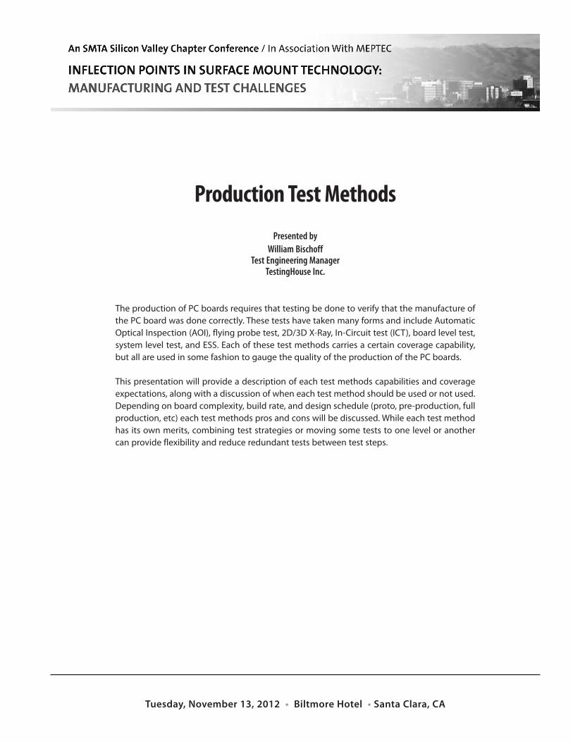
Production Test Methods
Presented byWilliam Bischoff
Test Engineering ManagerTestingHouse Inc.
The production of PC boards requires that testing be done to verify that the manufacture of the PC board was done correctly. These tests have taken many forms and include Automatic Optical Inspection (AOI), flying probe test, 2D/3D X-Ray, In-Circuit test (ICT), board level test, system level test, and ESS. Each of these test methods carries a certain coverage capability, but all are used in some fashion to gauge the quality of the production of the PC boards.
This presentation will provide a description of each test methods capabilities and coverage expectations, along with a discussion of when each test method should be used or not used. Depending on board complexity, build rate, and design schedule (proto, pre-production, full production, etc) each test methods pros and cons will be discussed. While each test method has its own merits, combining test strategies or moving some tests to one level or another can provide flexibility and reduce redundant tests between test steps.
Tuesday, November 13, 2012 • Biltmore Hotel • Santa Clara, CA

Flying Probe TestingOverview
Presented byPaul Bennett
Western Regional ManagerAcculogic Ltd.
As Flying Probe test systems have become more popular in the testing of PCBAs the need to increase test coverage has arisen as the key technology goal. To address this goal Flying Probers have augmented their traditional component electrical tests with other tech-nologies such as Boundary Scan, Automated Optical Inspection, Thermal Inspection, Laser Measurement, Automated Visual Inspection, Flying Bed-of-Nails and external instrumenta-tion. Flying Probers deploy these test technologies in unique combinations to fill in the test requirements of various PCBAs from low to high complexity. This presentation will review the capabilities and limitations of these other technologies with today’s Flying Probe systems.
Tuesday, November 13, 2012 • Biltmore Hotel • Santa Clara, CA

Boundary Scan and Board Assisted-BIST Long and Short Term Solutions for
Test Point Erosion
Presented bySteve Butkovich
Test Strategy GroupCisco Systems Inc.
Escalating printed circuit board complexity and reduced test point access are driving a desire to increase the use of technologies such as Boundary-Scan and IC BIST (Integrated Circuit Built In Self Test) to improve test coverage. The increasing functionality and Input/Output (IO) speed of integrated circuits and the corresponding increase in high density interconnect in PCBs can lead to higher costs of test and loss of test coverage. New product design solutions (in terms of testability features and functions) need to be explored, that facilitate lower test cost solutions, while keeping adequate test coverage.
Two areas of industry collaboration to address these issues, which are being coordinated through the International Electronics Manufacturing Initiative (iNEMI) Test Technology Integration Group (TIG) will be discussed here. In the first area, the Boundary Scan Adoption team is currently researching the structural test of external memory devices. The project team has evaluated the pros, cons and limitations of current and upcoming boundary-scan and DFT technology solutions. An analysis of current and future best practices using combinations of test methods and DFT technologies was undertaken and will be used to increase industry awareness of the memory device structural test issue and associated DFT technologies.
Tuesday, November 13, 2012 • Biltmore Hotel • Santa Clara, CA
PANEL DISCUSSION
Manufacturing and Test Challenges The session leaders will summarize the information from the specific sessions with a group discussion including the speakers and attendees of potential solutions and future work needed to address the issues highlighted.
Tuesday, November 13, 2012 • Biltmore Hotel • Santa Clara, CA

About MEPTEC
MEPTEC (MicroElectronics Packaging and Test Engineering Council) is a trade association of semiconductor suppli-ers, manufacturers, and vendors concerned exclusively with packaging, assembly, and testing, and is committed to enhancing the competitiveness of the back-end portion of the semiconductor industry. Since its inception over 30 years ago, MEPTEC has provided a forum for semiconductor packaging and test professionals to learn and exchange ideas that relate to packaging, assembly, test and handling. Through our monthly luncheons, and one-day sympo-siums, and an Advisory Board consisting of individuals from all segments of the semiconductor industry, MEPTEC continuously strives to improve and elevate the roles of assembly and test professionals in the industry. For more information about MEPTEC events and membership visit www.meptec.org.
About SMTA
The SMTA (Surface Mount Technology Association) membership is an international network of professionals who build skills, share practical experience and develop solutions in electronic assembly technologies, including micro-systems, emerging technologies, and related business operations. For more information about SMTA events and membership visit www.smta.org.
PO Box 222, Medicine Park, OK 73557Tel: 650-714-1570 www.meptec.org
5200 Willson Road, Suite 215, Edina, MN 55424Tel: 952-920-7682
www.smta.org