INF3410/4411, Fall 2018
60
INF3410/4411, Fall 2018 Philipp Häfliger [email protected] Excerpt of Sedra/Smith Chapter 9: Frequency Response of Basic CMOS Amplifiers
Transcript of INF3410/4411, Fall 2018

INF3410/4411, Fall 2018
Philipp Hä[email protected]
Excerpt of Sedra/Smith Chapter 9: Frequency Response ofBasic CMOS Amplifiers

Content
High Frequency Small Signal Model of MOSFETs (book 9.2)
High Frequency Response of CS and CE Amplifiers (book 9.3)
Toolset for Frequency Analysis and Complete CS Analysis (9.4)
CG and Cascode HF response (Book 9.5)
Source follower HF response (Book 9.6)
Differential Amp HF Analysis (book 9.7)

MOSFET IC transfer function

BW and GB(P)
GB=BW ∗ AM
GB: gain bandwidth product, BW: bandwidth, AM : mid-band gain.There is usually a trade-off between BW and AM . If this trade off isinversely proportional, the GB is constant, e.g. in opamp feedbackconfigurations.
BW and GB(P) for CMOS integrated Circuits
For integrated circuits which normally have a pure low-passcharacteristics (i.e. no explicit AC-coupling at the input) you cansubstitute AM with ADC , i.e. the gain at DC. And:
BW = fH = f−3dB
Where fH is the high frequency cutoff and is the frequency at whichpoint AM i reduced by -3dB, i.e. the signal power is reduced by 1
2 ,as 10 log10
12 = 3.0

MOSFET ’Parasitic’ Capacitances Illustration

MOSFET ’Parasitic’ Capacitances Equations
Cgs = CoxW (23L + Lov ) (9.22)
Cgd = CoxWLov (9.23)
Csb/db =Csb0/db0√1+ VSB/DB
V0
(9.24/9.25)
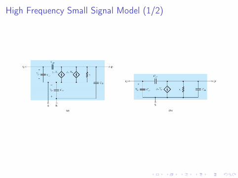
High Frequency Small Signal Model (1/2)
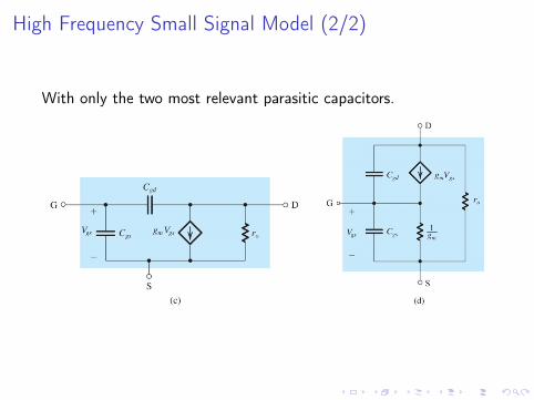
High Frequency Small Signal Model (2/2)
With only the two most relevant parasitic capacitors.

Unity Gain Frequency fT
Short circuit current gain. A measure for the best case transistorspeed.
Neglecting the current through Cgd :
ioii
=gm
s(Cgs + Cgd )(9.28)
fT =gm
2π(Cgs + Cgd )(9.29)

Trade-off fT vs Ao (i.e. GB)
fT =gm
2π(Cgs + Cgd )(9.29)
≈ 3µnVov
4πL2
A0 = gmro (7.40)
≈ 2λVov
=2L
λL︸︷︷︸const
Vov

Summary CMOS HF Small Signal Model

Content
High Frequency Small Signal Model of MOSFETs (book 9.2)
High Frequency Response of CS and CE Amplifiers (book 9.3)Interrupt: Transfer Function and Bode Plot
Toolset for Frequency Analysis and Complete CS Analysis (9.4)
CG and Cascode HF response (Book 9.5)
Source follower HF response (Book 9.6)
Differential Amp HF Analysis (book 9.7)

CS Amplifier HF small signal model

Using the Miller Effect
Note the simplyfying assumption that vo = gmrovgs , i.e. neglectingfeed forward contributions of igd which will still be very smallaround fH and makes the following a quite exact approximation ofthe dominant pole’s frequency fP ≈ fH

CS transfer function dominant Rsig(1/4)
vgs(s(Cgs + Ceq) +1
R ′sig) = vsig
1R ′sig

CS transfer function dominant Rsig(2/4)
vgs
vsig=
1R′
sig
s(Cgs + Ceq) +1
R′sig
vgs
vsig=
11+ sR ′sig (Cgs + Ceq)
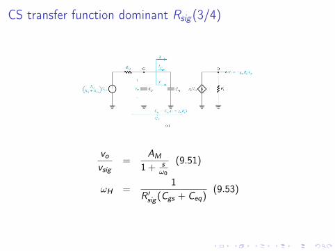
CS transfer function dominant Rsig(3/4)
vo
vsig=
AM
1+ sω0
(9.51)
ωH =1
R ′sig (Cgs + Ceq)(9.53)

CS transfer function dominant Rsig(4/4)

Interrupt: Transfer Function and Bode Plot

Transfer Function
The transfer function H(s) of a linear filter isI the Laplace transform of its impulse reponse h(t).I the Laplace transform of the differential equation describing
the I/O realtionship that is then solved for Vout(s)Vin(s)
I (this lecture!!!) the circuit diagram solved quite normally forVout(s)Vin(s)
by putting in impedances Z (s) for all linear elementsaccording to some simple rules.

Impedances of Linear Circuit Elements
resistor: Rcapacitor: 1
sCinductor: sL
Ideal sources (e.g. the id = gmvgs sources in small signal models ofFETs) are left as they are.

Transfer Function in Root Form
Transfer functions H(s) for linear electronic circuits can be writtenas dividing two polynomials of s.
H(s) =a0 + a1s + ...+ amsm
1+ b1s + ...+ bnsn
H(s) is often written as products of first order terms in bothnominator and denominator in the following root form, which isconveniently showing some properties of the Bode-plots. More ofthat later.
H(s) = a0(1+ s
z1)(1+ s
z2)...(1+ s
zm)
(1+ sω1)(1+ s
ω2)...(1+ s
ωn)

Bode Plots
Plots of magnitude (e.g. |H(s)|) in dB and phase e.g. ∠H(s) or φ)vs. log(ω).
In general for transfer functions with only realpoles and no zeros (pure low-pass): a) ω → 0+|H(s)| is constant at the low frequency gainand ∠H(s) = 0o b) for each pole as ωincreases the slope of |H(s)| increses by− 20dB
decade c) each pole contributes -90o to thephase, but in a smooth transistion so that at afrequency exactly at the pole it is exactly -45o

General rules of thumb to use real zeros and poles for Bodeplots (1/3)
a) find a frequency ωmid with equal number kof zeros and poles wherez1, ..., zk , ω1, ..., ωk < ωmid ⇒
|H(s)| ≈ K|z(k+1)...|zm||ω(k+1)|...|ωn|
∠H(s) ≈ 0o
and the gradient of both |H(s)| and ∠H(s) iszero

General rules of thumb to use real zeros and poles for Bodeplots (2/3)
b) moving from ωmid in the magnitude plot ateach |ωi | add -20dB/decade to the magnitudegradient and for each |zi | add +20dB/decadec) moving from ωmid in the phase plot tohigher frequencies at each ωi add -90o to thephase in a smooth transition (respectively−45o right at the poles) and vice versa towardslower frequencies.

General rules of thumb to use real zeros and poles for Bodeplots (3/3)
d) For the zeros towards higher frequencies ifthe nominater is of the form (1+ s
zi) add +90o
and if its of the form (1− szi) (refered to as
right half plain zero as the solution for s of0 = (1− s
zi) is positive) add -90o to the phase
in a smooth transition (i.e. respectively ±45o
right at the zeros) and vice versa towards lowerfrequencies.
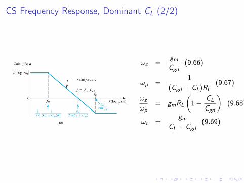
CS Frequency Response, Dominant CL (1/2)
vo(s(Cgd + CL) + GL) + gmvgs = vgssCgd
vo
vgs=
sCgd − gm
s(Cgd + CL) + GL
= −gmRL1− s Cgd
gm
s(Cgd + CL)RL + 1(9.65)
CS Frequency Response, Dominant CL (2/2)
ωz =gm
Cgd(9.66)
ωp =1
(Cgd + CL)RL(9.67)
ωz
ωp= gmRL
(1+
CL
Cgd
)(9.68)
ωt =gm
CL + Cgd(9.69)

Content
High Frequency Small Signal Model of MOSFETs (book 9.2)
High Frequency Response of CS and CE Amplifiers (book 9.3)
Toolset for Frequency Analysis and Complete CS Analysis (9.4)
CG and Cascode HF response (Book 9.5)
Source follower HF response (Book 9.6)
Differential Amp HF Analysis (book 9.7)

Notation in this Book
A(s) = AMFHs
FH(s) =(1+ s
ωz1)...(1+ s
ωzn)
(1+ sωp1
)...(1+ sωpm
)

Dominant Pole Approximation
If ωp1 < 4ωp2 and ωp1 < 4ωz1 then
A(S) ≈ 11+ s
ωp1
ωH ≈ ωp1

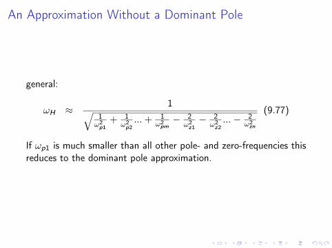
An Approximation Without a Dominant Pole
2nd order example
|FH(ωH)|2 =12
=(1+ ω2
Hω2
z1)(1+ ω2
Hω2
z2)
(1+ ω2H
ω2p1)(1+ ω2
Hω2
p2)
=1+ ω2
H
(1
ω2z1
+ 1ω2
z2
)+ ω4
H
(1
ω2z1ω
2z2
)1+ ω2
H
(1
ω2p1
+ 1ω2
p2
)+ ω4
H
(1
ω2p1ω
2p2
)⇒ ωH ≈ 1√
1ω2
p1+ 1
ω2p2− 2
ω2z1− 2
ω2z2
(9.76)
An Approximation Without a Dominant Pole
general:
ωH ≈ 1√1
ω2p1
+ 1ω2
p2...+ 1
ω2pm− 2
ω2z1− 2
ω2z2...− 2
ω2zn
(9.77)
If ωp1 is much smaller than all other pole- and zero-frequencies thisreduces to the dominant pole approximation.

Open-Circuit Time Constants Method
ωH ≈1∑
i CiRi
Where Ci are all capacitors in the circuit and Ri is the resistanceseen by Ci when the input signal source is zeroed and all othercapacitors are open circuited.

Open-Circuit Time Constants Method Example CS Amp

The Difficult One is Rgd
ix = − vgs
Rsig
=vgs + vx
RL+ vgsgm
=vx
RL− ixRsig
(1RL
+ gm
)Rgd =
vx
ix= [RL + Rsig (1+ gmRL)]

Open Circuit Time Constant
τH = RsigCgs + RLCL + [RL + Rsig (1+ gmRL)]Cgd
= Rsig[Cgs + (1+ gmRL)Cgd
]+ RL
[Cgd + CL
](9.88)
Previously:
ωH =1
R ′sig (Cgs + (1+ gmRL)Cgd )(9.53)
ωH =1
(Cgd + CL)RL(9.67)

Comparing Approximations
If you combine the prviously transfer functions for vgsvsig
derived from(9.46) and vo
vgsfrom (9.65) as A(s) = vgs
vsig
vovgs
you get both of theseprevious ωH as poles and can compute the combined ωH accordingto (9.77):
τH =1ωH≈√
[R ′sig (Cgs + Ceq)]2 + [(Cgd + CL)RL]2 (9.77)
So the geometric mean rather than the sum ...

Content
High Frequency Small Signal Model of MOSFETs (book 9.2)
High Frequency Response of CS and CE Amplifiers (book 9.3)
Toolset for Frequency Analysis and Complete CS Analysis (9.4)
CG and Cascode HF response (Book 9.5)
Source follower HF response (Book 9.6)
Differential Amp HF Analysis (book 9.7)

CG Amplifier HF Response
NOTE: no Miller effect!

CG Amplifier HF Response T-model

CG Amplifier HF Response without ro
τp1 = Cgs
(Rsig ||
1gm
)τp2 = (Cgd + CL)RL

CG Amplifier open circuit time-constant with ro for Cgs
τgs = Cgs
(Rsig ||
ro + RL
gmro
)

CG Amplifier open circuit time-constant with ro for Cgd +CL
τgd = (Cgd + CL) (Rsig ||(ro + Rsig + gmroRsig ))

CG Amplifier HF Response Conclusion
No Miller effect that would cause low impedance at highfrequencies, but due to low input resistance the impedance isalready low at DC ⇒ low AM for Rsig > 0

Cascode Amplifier HF Response
τgs1 = Cgs1Rsig
τgd1 = Cgd1 [(1+ gm1Rd1)Rsig + Rd1]
where Rd1 = ro1||ro2 + RL
gm2ro2
τgs2 = (Cgs2 + Cdb1)Rd1
τgd2 = (CL + Cgd2)(RL||(ro2 + ro1 + gm2ro2ro1))
τh ≈ τgs1 + τgd1 + τgs2 + τgd2

Cascode Amplifier HF Response
Rearranging τh grouping by the three nodes’resistors:
τh ≈ Rsig[Cgs1 + Cgd1(1+ gm1Rd1)
]+Rd1(Cgd1 + Cgs2 + Cdb1)
+(RL||Ro)(CL + Cgd2)
Thus, if Rsig > 0 and terms with Rsig are dominantone can either get larger bandwidth at the sameDC gain than a CS amplifier when RL ≈ ro or getmore DC gain at the same bandwith than a CSamplifier when RL ≈ gmr2
o or increase bothbandwith and DC gain to less than their maximumby tuning RL somewhere inbetween.

Cascode Amplifier HF Response
Rearranging τh grouping by the three nodes’resistors:
τh ≈ Rsig[Cgs1 + Cgd1(1+ gm1Rd1)
]+Rd1(Cgd1 + Cgs2 + Cdb1)
+(RL||Ro)(CL + Cgd2)
With Rsig ≈ 0 one can trade higher BW forreduced ADC or higher ADC for reduced BWcompared to a CS amp, keeping the unity gainfrequency (i.e. the GB) constant.

Cascode vs CSCS:
ADC = −gm(ro ||RL)
τH = Rsig[Cgs + (1+ gm(ro ||RL))Cgd
]+ (ro ||RL)
[Cgd + CL
]Cascode:
ADC = (−gm1(RO ||RL)
where RO = gm2ro2ro1
τH = Rsig[Cgs1 + Cgd1(1+ gm1Rd1)
]+Rd1(Cgd1 + Cgs2 + Cdb1)
+(RL||Ro)(CL + Cgd2)
where Rd1 = ro1||ro2 + RL
gm2ro2

Content
High Frequency Small Signal Model of MOSFETs (book 9.2)
High Frequency Response of CS and CE Amplifiers (book 9.3)
Toolset for Frequency Analysis and Complete CS Analysis (9.4)
CG and Cascode HF response (Book 9.5)
Source follower HF response (Book 9.6)
Differential Amp HF Analysis (book 9.7)

Source Follower HF Response
A(s) = AM
1+(
sωz
)1+ b1s + b2s2 = AM
1+(
sωz
)1+ 1
Qsω0
+ s2
ω20

Source Follower Frequency Response Possibilities
ωp1,p2 =− 1
Qω0±√
1ω2
0Q2 − 4 1ω2
0
2

Intuition for Resonance/Instability

Dependence on Q-factor (1/2)
-2 -1.5 -1 -0.5 0 0.5 1 1.5 2Re(A)
-2
-1.5
-1
-0.5
0
0.5
1
1.5
2
Im(A)
One Real Pole ωp1
=1/1000
1/A(j ω)A(j* ω)|j*[10 0 ,10 5 ]
A(j* ω)|j* ω=j*10 0
A(j* ω)|j* ω=j*10 3
j*ω=j*10 5
-2 -1.5 -1 -0.5 0 0.5 1 1.5 2Re(A)
-2
-1.5
-1
-0.5
0
0.5
1
1.5
2
Im(A)
Two Identical Real Poles: ω0
=1/1000 and Q=0.5
1/A(j ω)A(j* ω)|j*[10 0 ,10 5 ]
A(j* ω)|j* ω=j*10 0
A(j* ω)|j* ω=j*10 3
j*ω=j*10 5

Dependence on Q-factor (2/2)
-2 -1.5 -1 -0.5 0 0.5 1 1.5 2Re(A)
-2
-1.5
-1
-0.5
0
0.5
1
1.5
2
Im(A)
Two Complex Poles: ω0
=1/1000 and Q=0.707
1/A(j ω)A(j* ω)|j*[10 0 ,10 5 ]
A(j* ω)|j* ω=j*10 0
A(j* ω)|j* ω=j*10 3
j*ω=j*10 5
-2 -1.5 -1 -0.5 0 0.5 1 1.5 2Re(A)
-2
-1.5
-1
-0.5
0
0.5
1
1.5
2
Im(A)
Two Complex Poles: ω0
=1/1000 and Q=1.0
1/A(j ω)A(j* ω)|j*[10 0 ,10 5 ]
A(j* ω)|j* ω=j*10 0
A(j* ω)|j* ω=j*10 3
j*ω=j*10 5

Content
High Frequency Small Signal Model of MOSFETs (book 9.2)
High Frequency Response of CS and CE Amplifiers (book 9.3)
Toolset for Frequency Analysis and Complete CS Analysis (9.4)
CG and Cascode HF response (Book 9.5)
Source follower HF response (Book 9.6)
Differential Amp HF Analysis (book 9.7)

HF Analysis of Current-Mirror-Loaded CMOS Amp (1/2)
Neglecting ro in current mirror:
GM = gm1+ s Cm
2gm3
1+ s Cmgm3
ωp2 =gm3
Cm
ωz =2gm3
Cm

HF Analysis of Current-Mirror-Loaded CMOS Amp (2/2)
vo = vidGMZo
vo
vid= gm3Ro
(1+ s Cm
2gm3
1+ s Cmgm3
)(1
Ro + 1sCLRo
)
ωp1 =1
CLRo
And ωp1 is usually clearlydominant.