![Inertial Navigation Systems - Indico [Home]indico.ictp.it/event/a12180/session/23/contribution/14/material/0/... · Inertial Navigation Systems. Inertial Navigation Systems ... •](https://static.fdocuments.us/doc/165x107/5a94bdc87f8b9a451b8c1652/inertial-navigation-systems-indico-home-navigation-systems-inertial-navigation.jpg)
Inertial displacement of a domain wall excited by ultra...
45
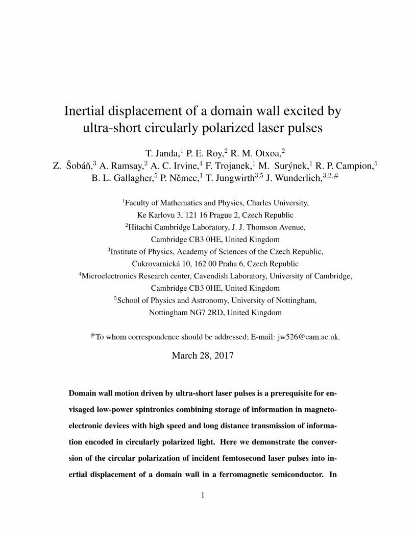
Inertial displacement of a domain wall excited by ultra-short circularly polarized laser pulses T. Janda, 1 P. E. Roy, 2 R. M. Otxoa, 2 Z. ˇ Sob´ aˇ n, 3 A. Ramsay, 2 A. C. Irvine, 4 F. Trojanek, 1 M. Sur´ ynek, 1 R. P. Campion, 5 B. L. Gallagher, 5 P. Nˇ emec, 1 T. Jungwirth 3,5 J. Wunderlich, 3,2,# 1 Faculty of Mathematics and Physics, Charles University, Ke Karlovu 3, 121 16 Prague 2, Czech Republic 2 Hitachi Cambridge Laboratory, J. J. Thomson Avenue, Cambridge CB3 0HE, United Kingdom 3 Institute of Physics, Academy of Sciences of the Czech Republic, Cukrovarnick´ a 10, 162 00 Praha 6, Czech Republic 4 Microelectronics Research center, Cavendish Laboratory, University of Cambridge, Cambridge CB3 0HE, United Kingdom 5 School of Physics and Astronomy, University of Nottingham, Nottingham NG7 2RD, United Kingdom # To whom correspondence should be addressed; E-mail: [email protected]. March 28, 2017 Domain wall motion driven by ultra-short laser pulses is a prerequisite for en- visaged low-power spintronics combining storage of information in magneto- electronic devices with high speed and long distance transmission of informa- tion encoded in circularly polarized light. Here we demonstrate the conver- sion of the circular polarization of incident femtosecond laser pulses into in- ertial displacement of a domain wall in a ferromagnetic semiconductor. In 1
-
Upload
hoangtuong -
Category
Documents
-
view
221 -
download
0
Transcript of Inertial displacement of a domain wall excited by ultra...
Inertial displacement of a domain wall excited byultra-short circularly polarized laser pulses
T. Janda,1 P. E. Roy,2 R. M. Otxoa,2
Z. Soban,3 A. Ramsay,2 A. C. Irvine,4 F. Trojanek,1 M. Surynek,1 R. P. Campion,5
B. L. Gallagher,5 P. Nemec,1 T. Jungwirth3,5 J. Wunderlich,3,2,#
1Faculty of Mathematics and Physics, Charles University,Ke Karlovu 3, 121 16 Prague 2, Czech Republic
2Hitachi Cambridge Laboratory, J. J. Thomson Avenue,Cambridge CB3 0HE, United Kingdom
3Institute of Physics, Academy of Sciences of the Czech Republic,Cukrovarnicka 10, 162 00 Praha 6, Czech Republic
4Microelectronics Research center, Cavendish Laboratory, University of Cambridge,Cambridge CB3 0HE, United Kingdom
5School of Physics and Astronomy, University of Nottingham,Nottingham NG7 2RD, United Kingdom
#To whom correspondence should be addressed; E-mail: [email protected].
March 28, 2017
Domain wall motion driven by ultra-short laser pulses is a prerequisite for en-
visaged low-power spintronics combining storage of information in magneto-
electronic devices with high speed and long distance transmission of informa-
tion encoded in circularly polarized light. Here we demonstrate the conver-
sion of the circular polarization of incident femtosecond laser pulses into in-
ertial displacement of a domain wall in a ferromagnetic semiconductor. In
1
our study we combine electrical measurements and magneto-optical imaging
of the domain wall displacement with micromagnetic simulations. The optical
spin transfer torque acts over a picosecond recombination time of the spin-
polarized photo-carriers which only leads to a deformation of the internal do-
main wall structure. We show that subsequent depinning and micro-meter
distance displacement without an applied magnetic field or any other external
stimuli can only occur due to the inertia of the domain wall.
DWs driven by short field (1) or current (2, 3) pulses of length 1 10 ns and moving
at characteristic velocities reaching 0.1 1 µm/ns (4) are displaced over the duration of the
pulse by distances at least comparable but typically safely exceeding the domain wall width. In
this regime inertia, causing a delayed response to the driving field and a transient displacement
after the pulse, is not the necessary prerequisite for the device operation and is rather viewed
as negative factor. It can set the operation frequency limit of the DW device and potentially
affect precise positioning of the DW by the driving pulse. Realizing massless DW dynamics is
therefore one of the goals in the research of field-driven and current-driven DWs (5).
The aim of our study is the demonstration of a micrometer-scale DW displacement by
circularly-polarized, ultra-short laser pulses (LPs). Our experiments are in the regime where
the external force generated by the LP acts on the picosecond time-scale over which the ex-
pected sub-nanometer DW displacement would be orders of magnitude smaller than the DW
width and insufficient for any practical DW device implementation. Inertia allowing for a free
transient DW motion is the key here that enables the operation of the DW devices in the regime
of the ultra-short optical excitations, rather than being a factor limiting the operation of the
opto-spintronic DW devices.
Our study links the physics of inertial DW motion with the field of optical recording of
magnetic media. The manipulation of magnetism by circularly polarized light, demonstrated
2
already in ferrimagnets (6), transition metal ferromagnets (7), and ferromagnetic semiconduc-
tors (8), has become an extensively explored alternative to magnetic field or current induced
magnetization switching. Our work demonstrates that optical recording can in principle be fea-
sible at low power when realized via an energy-efficient DW displacement driven by ultra-short
LPs and without the need to heat the system close to the Curie temperature.
The III-V based ferromagnetic semiconductor used in our study is an ideal model system
for the proof of concept demonstration, as well as, for the detailed theoretical analysis of the
DW dynamics in this new regime. DWs in out-of-plane magnetized (Ga,Mn)(As,P) have a sim-
ple Bloch wall structure with low extrinsic pinning (9). The non-thermal optical spin transfer
torque (oSTT) mechanism which couples the circular polarization of the incident light to the
magnetization via spin-polarized photo-carriers is microscopically well understood in this fer-
romagnetic semiconductor material (10). In our experiments, individual circularly polarised
100 fs short LPs at normal incidence and separated by 10 ns expose an area with a single
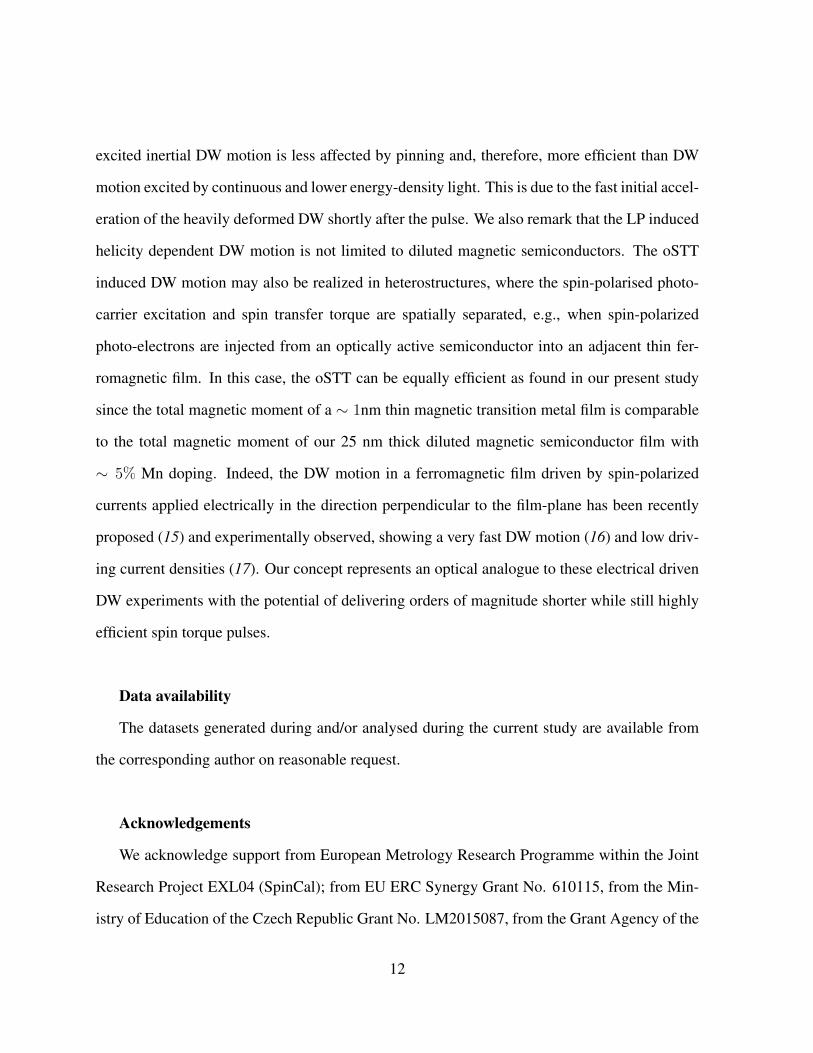
DW. As illustrated in figure 1A, the generated perpendicular-to-plane spin-polarised photoelec-
trons exert the oSTT only in the region with an in-plane component of the magnetization, i.e. in
the DW. The action of the oSTT is limited by the photoelectron recombination time 10 ps.
To probe the inertial DW motion, we make use of elastic properties of a uniformly propa-
gating DW. In this case, the DW propagates continuously and remains connected so that local
DW pinning affects the entire wall over its whole extension. First, the Oersted field generated
in a stripe line above the magnetic bar nucleates a reversed magnetic domain. Then, a single
DW is driven towards a cross structure by a small external magnetic field of a slightly larger
magnitude than the propagation field BPR. The low BPR of 0.1 mT found in our bar devices
patterned from an epitaxially grown Ga0.94Mn0.06As0.91P0.09 25 nm thick film implies a very
small DW pinning on structural defects and inhomogeneities. In this case, DW propagation is
3
uniform and a straight DW becomes pinned at the entrance of the cross structure as shown in
figure 1B. To continue the DW propagation through the cross, the DW must increase its length
which is accompanied by an increase in its magnetic energy. This results in a restoring force
which can be expressed in terms of a virtual restoring field BR(x) that depends on the position
x of the DW. Here, BR(x) acts as to always drive the DW back to the cross entrance. The mag-
netic field driven expansion of a DW pinned at the cross entrance is analogous to the inflation of
a two-dimensional soap-bubble (see figure 2A). The DW depins when the applied field exceeds
the maximum restoring field B
maxR (11). Within this model, BR(x) reaches its maximum value
|BmaxR | = /(MS · w) at the cross center at x = 0 (figure 3A) and the DW can only depin once
it passes the cross center. Here, = 4pAKE is the DW energy per unit area, KE the effective
perpendicular anisotropy coefficient, A the exchange stiffness, MS the saturation magnetization
and w is the width of the bar. The DW can be depinned from the cross by either an applied
magnetic field BA > |BmaxR | or by the oSTT. We can therefore use |BA| |Bmax
R | to calibrate
the strength of the oSTT.First, however, we have to confirm the elastic nature of DWs in our
devices, and verify the applicability of the bubble-like DW model of figure 2A.
Results
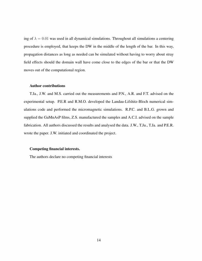
Elastic domain wall pinning. We performed magnetic field driven DW motion experiments
without optical excitation. Depinning fields for three different devices with bar widths of 2,
4 and 6 µm are shown in figure 3C as a function of the inverse bar width. The slope of the
linear fit agrees with that obtained from the measured effective perpendicular anisotropy, KE =
1200 J/m3, the saturation magnetization, MS = 18 kA/m, and assuming the exchange stiffness,
A = 50 fJ/m, which is a reasonable estimate for our GaMnAsP film (9). The elastic behaviour
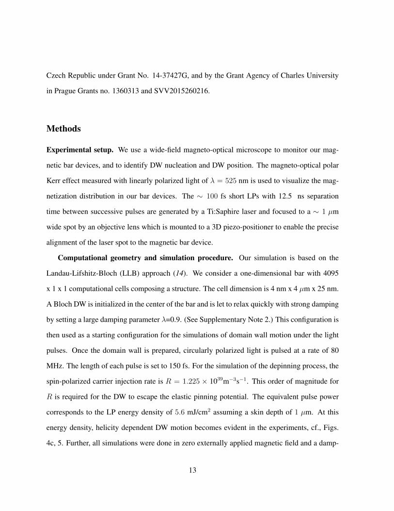
of the
pA/KE 20 nm wide DW is also confirmed by MOKE images of the 6 µm wide bar
device shown in figure 2B-D . In figure 2B, the DW bends into a bubble-like shape under the
4
influence of an applied field BA = 0.25 mT. Figure 2C shows that the restoring field drives the
DW back to the cross-entrance after BA is turned-off. Figure 2D displays the difference between
the two MOKE images in figure 2B and figure 2C, confirming the bubble like shape of the DW.
In addition, anomalous Hall effect (AHE) measurements performed on the 4 µm device under
an alternating field excitationBA = B0|sin(! · t)| also confirm the elastic DW behaviour (figure
3B). If B0 does not exceed |BmaxR |, e.g., for B0 = 0.2 mT (green), and B0 = 0.3 mT (blue), the
periodic variation of the AHE signal indicates that the DW is at the position x where BR(x) and
BA(t) compensate. The residual AHE signal at BA = 0 of about 10 % of the maximum AHE
signal at reversed saturation (DW depinned from the cross) corresponds to the AHE-response
for the magnetization distribution with a straight DW located at the cross entrance. (For more
details see Supplementary Note 1.)
Helicity dependent domain wall excitation by 100 fs laser pulses. We now combine the
elastic pinning properties of the DW at the cross with the light induced excitation experiments
in order to proof the inertial character of the oSTT-induced DW motion. The basic idea of
our experiment is to exploit the elastic restoring force which acts continuously throughout the
entire cross (of a width up to 6 µm in our study) against the expansion of the DW which is
driven by individual 100 fs LPs. The photo-generated electrons can transfer their spin to
the magnetization only during their 10 ps lifetime which is 3 orders of magnitude shorter
than the pulse separation time of 10 ns. The measurements shown in figure 3 are performed
at a 90 K sample temperature. We obtain similar results when performing the measurements
also at higher (95 K) and at lower (75 K) sample temperatures, as shown in Supplementary
Note 1. At these temperatures, LPs with a wavelength = 750 nm excite photo-electrons
slightly above the bottom of the GaAs conduction band so that for a circularly polarized incident
light, photo-electrons become spin-polarized with the degree of polarization approaching the
maximum theoretical value of 50% (12). To avoid the difficulty with aligning our 1 µm
5
Gaussian spot on top of a 20 nm wide DW, we employ the experimental procedure sketched
in figure 4A. First, a straight DW is positioned at the cross entrance. Then, the LP spot is
placed 10 µm away from the DW on the reversed domain side and a magnetic field BA with
B
0DP( +0.4 mT ) > BA > BPR( 0.1mT ) is applied. (B0
DP is the DW depinning field
without LP irradiation.) In this field range and without LP irradiation, the DW remains pinned
at the cross entrance. The LP spot is then swept at a rate of 2 µm/ms for 20 µm along the bar
so that the initial DW position is crossed by the spot and approximately 100000 ultra-short
LPs time-separated by 10 ns expose the DW. The lowest applied magnetic field at which the
DW depins from the cross in the presence of LPs is labeled BDP. The dependencies of BDP on
the LP energy density for circularly polarized
+, and linearly polarized
0 LPs are shown
in figure 4B. First, we recognize a reduction of BDP with increasing energy density for all three
LP polarizations. In case of the linear polarization, i.e., without the oSTT contribution, we
attribute the reduction of BDP(0) only to the LP induced sample heating. Importantly, we do
not observe DW depinning without applying BA > 0 up to the highest LP energy densities
used in our experiments of more than 30 mJ/cm2. At large LP energy densities above
20 mJ/cm2 we observe a saturation of BDP(0) with increasing LP energy density implying that
LP heating does not increase anymore. We assign this behaviour to the saturation of photo-
carriers generated at very high LP energy densities.
For circularly polarized LPs, an additional contribution from the oSTT is present. We ob-
serve for all measured LP energy densities that BDP(+) < BDP(0) < BDP() for the posi-
tive magnetization orientation of the nucleated domain. In case of + polarised LPs and at high
enough LP energy densities (above 12 mJ/cm2) the DW depins without an applied magnetic
field (and even at small negative applied magnetic field which opposes DW expansion).
For
polarized LPs and the same initial domain configuration, we do not observe the
zero-field DW depinning up to the highest LP energy density used in our experiments. Instead,
6
we again observe saturation of BDP() above 20 mJ/cm2. We attribute the difference in the
saturation values of BDP() and BDP(0) to the effect of the oSTT acting against depinning
for polarized LPs.
We estimate the LP heating related temperature increase by comparing BDP(0, LP energy
density, T = 90 K) measured at constant 90 K base temperature with the temperature de-
pendence of B0DP(T ) without LP irradiation. We found that for LP energy densities of up to
35 mJ/cm2, the temperature increase does not exceed the Curie temperature of 115 K of the
GaMnAsP film.
The differential MOKE image in figure 4C shows an example of the domain configuration
after the DW has depinned from the cross entrance by optical excitation in conjunction with
a constant applied magnetic field BA which is larger than the DW propagation field of the bar
outside the cross. After depinning from the cross irradiated by polarized LPs, the DW becomes
pinned again at a second cross which was not irradiated during the experiment. Figure 4D
shows the final domain configuration after DW depinning by
+ polarised LPs at zero applied
magnetic field. In this case, the
+ polarized LPs depin and drive the DW forward to the final
irradiated spot position.
Inertial domain wall propagation. From the measurements shown in figure 4 we can con-
clude that for the given initial domain configuration, the oSTT generated by
+ () polarised
LPs assists (opposes) DW depinning. The measurements confirm that only
+ polarised LPs
can move the DW beyond the maximum of the pinning barrier at the cross center. Consid-
ering the 100 fs short and 10 ns time-seperated LPs, depinning of the DW by the oSTT
becomes only possible if the elastically pinned DW propagates forward in between successive
LPs. Depinning by a DW motion without inertia would require DW velocities of more than
1 km/s which are unrealistically high for the DW motion in GaMnAsP films where the max-
imum magnon velocity is of similar magnitude and where we have observed and calculated
7
Walker break down velocities 10 m/s for the oSTT, current and field driven DW motion (9).
(See also Supplementary Note 2.)
To verify our interpretation, we repeated our measurements at the inverted magnetization
configuration in which the reversed magnetization of the nucleated domain points in the negative
(m
Rz
) direction. In this case, the oSTT should act in the opposite direction. Indeed, we observe
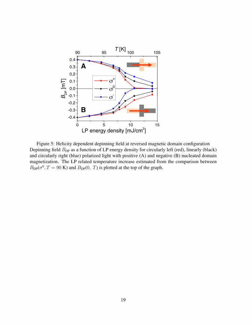
the opposite helicity dependency in our experiments. Figure 5 shows measurements on a 4 µm
wide device comparing the two magnetisation configurations. The consistency found between
BDP(+(),+m
Rz
) BDP((+),m
Rz
) and BDP(0,+m
Rz
) BDP(0,m
Rz
) confirms the
oSTT mechanism and the high reproducibility of our measurements.
Note, that a heat-gradient can in principle also drive the DW motion (13). The heat-gradient
driven motion can become helicity dependent if the light absorption in the two adjacent mag-
netic domains is helicity-dependent due to the magnetic circular dichroism (MCD). In our ex-
periments, such a scenario is unlikely because about 98% of the LP light penetrates through
the 25nm thick magnetic GaMnAsP film and is absorbed and transformed into the heat in the
GaAs substrate with no dependence on the helicity.
An indication that the MCD is not the origin of the observed helicity dependent DW de-
pinning is given by helicity-dependent DW experiments shown in the Supplementary Note 3.
The experiments are performed at photon-energies ranging from below the band-gap up to high
energies where the net spin-polarization of photo-electrons is reduced due to the excitation
from the spin-orbit split-off band. We do not observe the helicity-dependent DW depinning at
photon-energies where MCD of GaMnAsP is still present while simultaneously the photoelec-
tron polarisation is strongly reduced.
To investigate the effect of the MCD on the helicity dependent DW motion in more detail,
we present additional experiments in the Supplementary Note 3 which allow us to identify the
sign and estimate the magnitude of the temperature gradient generated by the MCD between
8

two opposite magnetized domains. We found that the MCD-generated heat-gradient is smaller
than the helicity independent heat-gradient generated by the Gaussian LP spot, and more im-
portantly, that the DW motion induced by the MCD is in the opposite direction to the observed
helicity dependent DW motion. This excludes unambiguously the MCD as the origin of our
experimental observations.
To further analyze heat-gradient related DW drag effects due to the non-uniform heating by
the Gaussian-shaped LP spot, we have performed measurements with opposite laser spot sweep
directions. In this case, the heat-gradient with respect to the initial DW position is inverted. As
shown in the Supplementary Note 3, sweeping the LP spot along the bar from an initial position
outside of the nucleated domain to the final position in the nucleated domain does not change
the helicity dependency of the depinning field. Additional measurements on devices with 2
and 6 µm wide bars have, apart from the stronger (weaker) DW pinning strength and larger
(smaller) temperature increase from LP heating in the 2 µm (6 µm) device, also confirmed that
BDP(+()) < BDP(0) < BDP((+)) for +()mRz
.
We now support our interpretation of the experiments by 1-dimensional Landau-Lifshitz-
Bloch (LLB) numerical simulations of the magnetization m (14), coupled to the precessional
dynamics of the spin-polarized photo-carrier density, s (10):
@m
@t
= mHeff ↵?
m
2m (mHeff) +
↵||
m
2(m ·Heff)m (1)
@s@t
=Jex
~meqs m +R(t)n s
rec(2)
In Eq. (1), m=M(T )/M0, with M0 denoting the saturation magnetization at zero tempera-
ture and is the gyromagnetic ratio. The first, second and third terms describe the preces-
sion, transverse relaxation and longitudinal relaxtion of m, respectively. The effective field
9
Heff = Hd+Hex+Hmf+Hk+HOSTT+Hr comprises demagnetizing field, exchange field, inter-
nal material field related to longitudinal magnetization relaxation, uniaxial magnetocrystalline
anisotropy field, oSTT field and a geometrical pinning field, respectively. The two parameters
↵?(T ) and ↵||(T ) represent the transverse and longitudinal damping, respectively. The oSTT
from s on m is taken into account by HOSTT = Jeff(T )µ0meqM0
s (with Jeff(T ) = Jexm2eq). For more
details see Supplementary Information.
Eq. (2) describes the time-evolution of the spin polarized photo-electron density s. The first
term is the precession of s around the exchange-field of m with the coupling strength Jex; meq
is the equilibrium magnetization normalized by the zero temperature saturation magnetization
M0. The second term describes the spin-polarised photo-electron injection rate R(t), which
is non-zero only during the 100 fs LP, and n is the helicity dependent spin-polarization of
the injected electrons. Depending on the light-helicity, n is [0 0 ± 1]. The last term describes
the decay of the spin density, determined primarily by the recombination time of the photo-
electrons, rec.
In the simulations, we consider a Bloch DW subjected to LPs and the restoring field BR(x)
as in figure 3A. BmaxR was set to a reduced value of 0.1 mT due to heat (deduced from figure
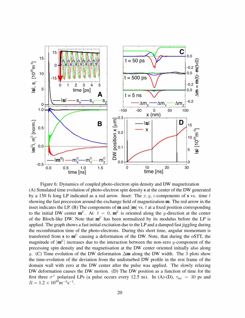
4B and described in the Supplementary Information). Figures 6 A,B show the simulated time
evolution of m and s at the initial DW center during and after the application of a single 150 fs
pulse with
+ ( n=[0 0 1]) polarization.
In figure 6A, the fast precession of s around the exchange field of m takes place until the
photo-electrons recombine. Only during this short time, angular momentum is transfered to m.
The precession of s is much faster than the dynamics of m so that a significant change of m due
to the precession around Heff happens after the photo-electrons recombined. Figure 6B shows
the time evolution of m at the center of the initial DW (m is initially directed along +y for the
Bloch DW). During the short oSTT, m is only weakly disturbed from its equilibrium direction.
10
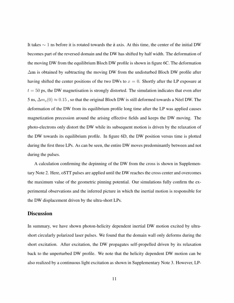
It takes 1 ns before it is rotated towards the z axis. At this time, the center of the initial DW
becomes part of the reversed domain and the DW has shifted by half width. The deformation of
the moving DW from the equilibrium Bloch DW profile is shown in figure 6C. The deformation
m is obtained by subtracting the moving DW from the undisturbed Bloch DW profile after
having shifted the center positions of the two DWs to x = 0. Shortly after the LP exposure at
t = 50 ps, the DW magnetisation is strongly distorted. The simulation indicates that even after
5 ns, m
x
(0) 0.15 , so that the original Bloch DW is still deformed towards a Neel DW. The
deformation of the DW from its equilibrium profile long time after the LP was applied causes
magnetization precession around the arising effective fields and keeps the DW moving. The
photo-electrons only distort the DW while its subsequent motion is driven by the relaxation of
the DW towards its equilibrium profile. In figure 6D, the DW position versus time is plotted
during the first three LPs. As can be seen, the entire DW moves predominantly between and not
during the pulses.
A calculation confirming the depinning of the DW from the cross is shown in Supplemen-
tary Note 2. Here, oSTT pulses are applied until the DW reaches the cross center and overcomes
the maximum value of the geometric pinning potential. Our simulations fully confirm the ex-
perimental observations and the inferred picture in which the inertial motion is responsible for
the DW displacement driven by the ultra-short LPs.
Discussion
In summary, we have shown photon-helicity dependent inertial DW motion excited by ultra-
short circularly polarized laser pulses. We found that the domain wall only deforms during the
short excitation. After excitation, the DW propagates self-propelled driven by its relaxation
back to the unperturbed DW profile. We note that the helicity dependent DW motion can be
also realized by a continuous light excitation as shown in Supplementary Note 3. However, LP-
11
excited inertial DW motion is less affected by pinning and, therefore, more efficient than DW
motion excited by continuous and lower energy-density light. This is due to the fast initial accel-
eration of the heavily deformed DW shortly after the pulse. We also remark that the LP induced
helicity dependent DW motion is not limited to diluted magnetic semiconductors. The oSTT
induced DW motion may also be realized in heterostructures, where the spin-polarised photo-
carrier excitation and spin transfer torque are spatially separated, e.g., when spin-polarized
photo-electrons are injected from an optically active semiconductor into an adjacent thin fer-
romagnetic film. In this case, the oSTT can be equally efficient as found in our present study
since the total magnetic moment of a 1nm thin magnetic transition metal film is comparable
to the total magnetic moment of our 25 nm thick diluted magnetic semiconductor film with
5% Mn doping. Indeed, the DW motion in a ferromagnetic film driven by spin-polarized
currents applied electrically in the direction perpendicular to the film-plane has been recently
proposed (15) and experimentally observed, showing a very fast DW motion (16) and low driv-
ing current densities (17). Our concept represents an optical analogue to these electrical driven
DW experiments with the potential of delivering orders of magnitude shorter while still highly
efficient spin torque pulses.
Data availability
The datasets generated during and/or analysed during the current study are available from
the corresponding author on reasonable request.
Acknowledgements
We acknowledge support from European Metrology Research Programme within the Joint
Research Project EXL04 (SpinCal); from EU ERC Synergy Grant No. 610115, from the Min-
istry of Education of the Czech Republic Grant No. LM2015087, from the Grant Agency of the
12
Czech Republic under Grant No. 14-37427G, and by the Grant Agency of Charles University
in Prague Grants no. 1360313 and SVV2015260216.
Methods
Experimental setup. We use a wide-field magneto-optical microscope to monitor our mag-
netic bar devices, and to identify DW nucleation and DW position. The magneto-optical polar
Kerr effect measured with linearly polarized light of = 525 nm is used to visualize the mag-
netization distribution in our bar devices. The 100 fs short LPs with 12.5 ns separation
time between successive pulses are generated by a Ti:Saphire laser and focused to a 1 µm
wide spot by an objective lens which is mounted to a 3D piezo-positioner to enable the precise
alignment of the laser spot to the magnetic bar device.
Computational geometry and simulation procedure. Our simulation is based on the
Landau-Lifshitz-Bloch (LLB) approach (14). We consider a one-dimensional bar with 4095
x 1 x 1 computational cells composing a structure. The cell dimension is 4 nm x 4 µm x 25 nm.
A Bloch DW is initialized in the center of the bar and is let to relax quickly with strong damping
by setting a large damping parameter =0.9. (See Supplementary Note 2.) This configuration is
then used as a starting configuration for the simulations of domain wall motion under the light
pulses. Once the domain wall is prepared, circularly polarized light is pulsed at a rate of 80
MHz. The length of each pulse is set to 150 fs. For the simulation of the depinning process, the
spin-polarized carrier injection rate is R = 1.225 1039m3s1. This order of magnitude for
R is required for the DW to escape the elastic pinning potential. The equivalent pulse power
corresponds to the LP energy density of 5.6 mJ/cm2 assuming a skin depth of 1 µm. At this
energy density, helicity dependent DW motion becomes evident in the experiments, cf., Figs.
4c, 5. Further, all simulations were done in zero externally applied magnetic field and a damp-
13
ing of = 0.01 was used in all dynamical simulations. Throughout all simulations a centering
procedure is employed, that keeps the DW in the middle of the length of the bar. In this way,
propagation distances as long as needed can be simulated without having to worry about stray
field effects should the domain wall have come close to the edges of the bar or that the DW
moves out of the computational region.
Author contributions
T.Ja., J.W. and M.S. carried out the measurements and P.N., A.R. and F.T. advised on the
experimental setup. P.E.R and R.M.O. developed the Landau-Lifshitz-Bloch numerical sim-
ulations code and performed the micromagnetic simulations. R.P.C. and B.L.G. grown and
supplied the GaMnAsP films, Z.S. manufactured the samples and A.C.I. advised on the sample
fabrication. All authors discussed the results and analysed the data. J.W., T.Ju., T.Ja. and P.E.R.
wrote the paper. J.W. initiated and coordinated the project.
Competing financial interests.
The authors declare no competing financial interests
14
sZ(σ+)
-sZ(σ-)y
z
σ+/σ-A B
DWBA
VHIN
ID
Z
Z
x
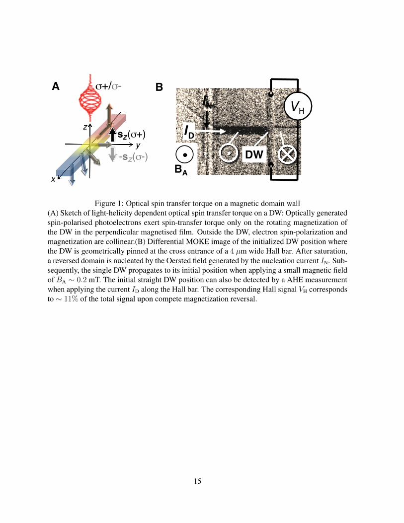
Figure 1: Optical spin transfer torque on a magnetic domain wall(A) Sketch of light-helicity dependent optical spin transfer torque on a DW: Optically generatedspin-polarised photoelectrons exert spin-transfer torque only on the rotating magnetization ofthe DW in the perpendicular magnetised film. Outside the DW, electron spin-polarization andmagnetization are collinear.(B) Differential MOKE image of the initialized DW position wherethe DW is geometrically pinned at the cross entrance of a 4 µm wide Hall bar. After saturation,a reversed domain is nucleated by the Oersted field generated by the nucleation current IN. Sub-sequently, the single DW propagates to its initial position when applying a small magnetic fieldof BA 0.2 mT. The initial straight DW position can also be detected by a AHE measurementwhen applying the current ID along the Hall bar. The corresponding Hall signal VH correspondsto 11% of the total signal upon compete magnetization reversal.
15
A
RBR
B
C
-w/2 0 w/2
BA D
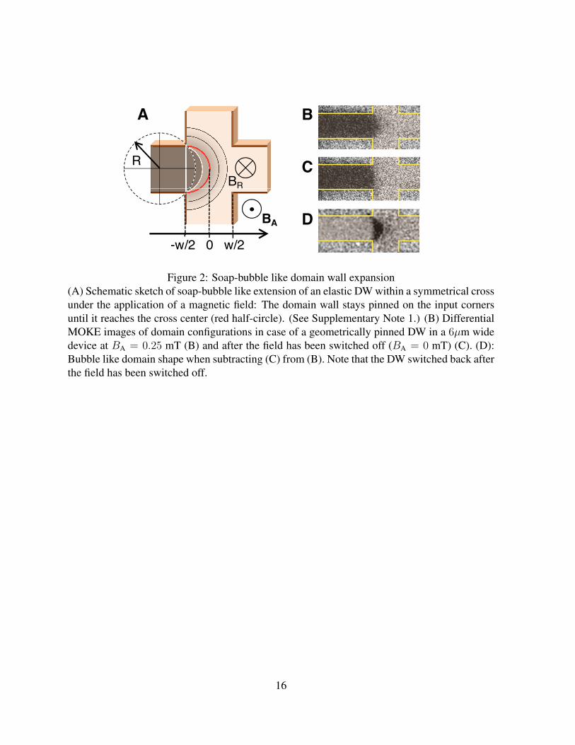
Figure 2: Soap-bubble like domain wall expansion(A) Schematic sketch of soap-bubble like extension of an elastic DW within a symmetrical crossunder the application of a magnetic field: The domain wall stays pinned on the input cornersuntil it reaches the cross center (red half-circle). (See Supplementary Note 1.) (B) DifferentialMOKE images of domain configurations in case of a geometrically pinned DW in a 6µm widedevice at BA = 0.25 mT (B) and after the field has been switched off (BA = 0 mT) (C). (D):Bubble like domain shape when subtracting (C) from (B). Note that the DW switched back afterthe field has been switched off.
16
0.4
0.5
0.6
0.7
P [m
T]
B
C
-1.0 -0.5 0.0 0.5 1.00.0
-0.1
-0.2
-0.3
-0.4BA [mT]
0.30.2
0.1
B R [m
T]
wall position x [w/2]
0.0
A
0.0 0.2 0.4 0.60.0
0.1
0.2
0.3
1/w [1/µm]
B 0 DP
0 20 40 60 800.00.20.40.60.81.0
∆R
AHE
[nor
m.]
time [s]
1.3mT 0.3mT 0.2mT B
BP = 0.11mT
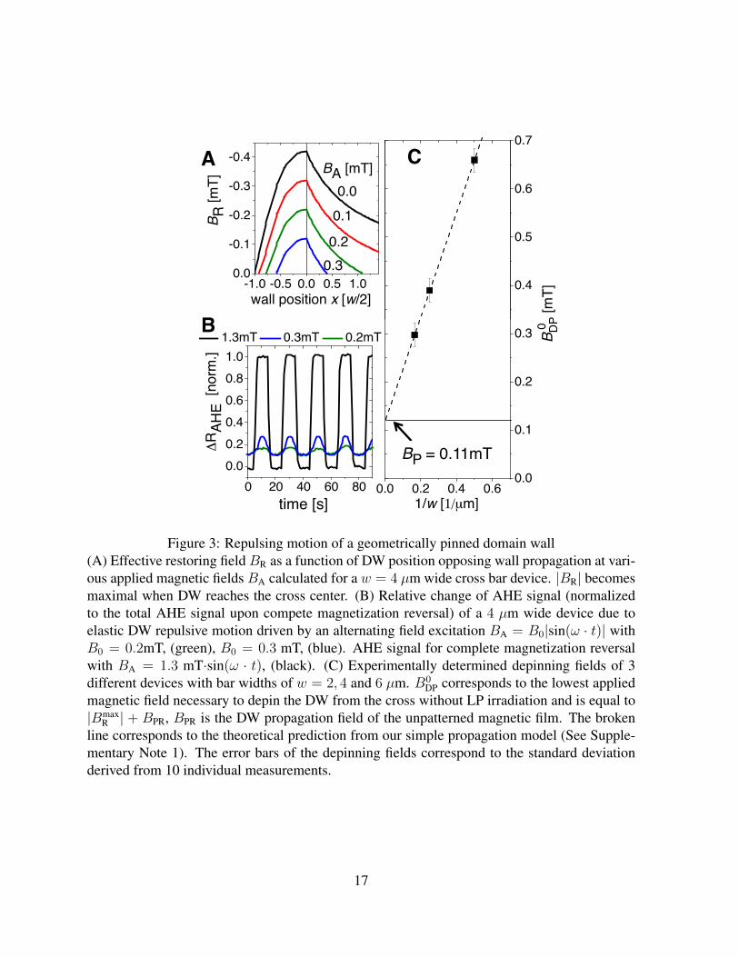
Figure 3: Repulsing motion of a geometrically pinned domain wall(A) Effective restoring field BR as a function of DW position opposing wall propagation at vari-ous applied magnetic fields BA calculated for a w = 4 µm wide cross bar device. |BR| becomesmaximal when DW reaches the cross center. (B) Relative change of AHE signal (normalizedto the total AHE signal upon compete magnetization reversal) of a 4 µm wide device due toelastic DW repulsive motion driven by an alternating field excitation BA = B0|sin(! · t)| withB0 = 0.2mT, (green), B0 = 0.3 mT, (blue). AHE signal for complete magnetization reversalwith BA = 1.3 mT·sin(! · t), (black). (C) Experimentally determined depinning fields of 3different devices with bar widths of w = 2, 4 and 6 µm. B0
DP corresponds to the lowest appliedmagnetic field necessary to depin the DW from the cross without LP irradiation and is equal to|Bmax
R | + BPR, BPR is the DW propagation field of the unpatterned magnetic film. The brokenline corresponds to the theoretical prediction from our simple propagation model (See Supple-mentary Note 1). The error bars of the depinning fields correspond to the standard deviationderived from 10 individual measurements.
17
Laser spotshift-trajectory
initially pinned DW
start stop
A
2nd cross entrance
C σ+, σ0, σ-0.2
0.3
0.4
T]
σ+ σ- σ0
B
D
PRA0DP BBB >>
0 10 20 30-0.1
0.0
0.1 B dp
[m
LP energy density [mJ/cm2]
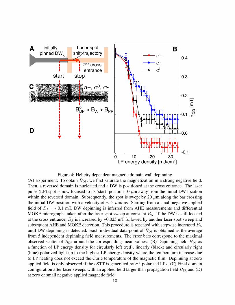
Figure 4: Helicity dependent magnetic domain wall depinning(A) Experiment: To obtain BDP, we first saturate the magnetization in a strong negative field.Then, a reversed domain is nucleated and a DW is positioned at the cross entrance. The laserpulse (LP) spot is now focused to its ’start’ position 10 µm away from the initial DW locationwithin the reversed domain. Subsequently, the spot is swept by 20 µm along the bar crossingthe initial DW position with a velocity of 2 µm/ms. Starting from a small negative appliedfield of BA = - 0.1 mT, DW depinning is inferred from AHE measurements and differentialMOKE micrographs taken after the laser spot sweep at constant BA. If the DW is still locatedat the cross entrance, BA is increased by +0.025 mT followed by another laser spot sweep andsubsequent AHE and MOKE detection. This procedure is repeated with stepwise increased BA
until DW depinning is detected. Each individual data-point of BDP is obtained as the averagefrom 5 independent depinning field measurements. The error bars correspond to the maximalobserved scatter of BDP around the corresponding mean values. (B) Depinning field BDP asa function of LP energy density for circularly left (red), linearly (black) and circularly right(blue) polarized light up to the highest LP energy density where the temperature increase dueto LP heating does not exceed the Curie temperature of the magnetic film. Depinning at zeroapplied field is only observed if the oSTT is generated by
+ polarised LPs. (C) Final domainconfiguration after laser sweeps with an applied field larger than propagation field BPR and (D)at zero or small negative applied magnetic field.
18
-0 1
0.0
0.1
0.2
0.3
0.4B D
P [m
T] σ+
σ0
-
90 95 100 105T [K]
A
0 5 10 15
-0.4
-0.3
-0.2
-0.1
LP energy density [mJ/cm2]
B σ
B
Figure 5: Helicity dependent depinning field at reversed magnetic domain configurationDepinning field BDP as a function of LP energy density for circularly left (red), linearly (black)and circularly right (blue) polarized light with positive (A) and negative (B) nucleated domainmagnetization. The LP related temperature increase estimated from the comparison betweenBDP(0
, T = 90 K) and BDP(0, T ) is plotted at the top of the graph.
19
1 00
5
10
15
|s| sX sY sZ
|s|,
s i [10
25m
-3]
0 1 2 3 4 5-15
0
15
time [ps]
A
-0.2
0.0t = 50 ps
-0.2
0.0
∆m
= m
(t)- m
(t<0)
t = 500 ps
100 50 0 50 100
-0.2
0.0
∆mX ∆mY ∆mZ
t = 5 ns
C
0.0 0.5 1.0 1.5-0.5
0.0
0.5
1.0
|mC| mCX mC
Y mCZ
|mC|,
mC i [n
orm
.]
time [ns]
B
0 10 20 300.0
0.1
0.2
0.3|s| x
time [ns]
D
W p
ositi
on x
[µm
]
0
5
10
15
|s| [
1025
m-3]
D
-100 -50 0 50 100 x (nm)
Figure 6: Dynamics of coupled photo-electron spin density and DW magnetization(A) Simulated time evolution of photo-electron spin density s at the center of the DW generatedby a 150 fs long LP indicated as a red arrow. Inset: The x, y, z-components of s vs. time t
showing the fast precession around the exchange field of magnetization m. The red arrow in theinset indicates the LP. (B) The components of m and |m| vs. t at a fixed position correspondingto the initial DW center mC. At t = 0, mC is oriented along the y-direction at the centerof the Bloch-like DW. Note that mC has been normalized by its modulus before the LP isapplied. The graph shows a fast initial excitation due to the LP and a damped fast jiggling duringthe recombination time of the photo-electrons. During this short time, angular momentum istransferred from s to mC causing a deformation of the DW. Note, that during the oSTT, themagnitude of |mC| increases due to the interaction between the non-zero y-component of theprecessing spin density and the magnetisation at the DW center oriented initially also alongy. (C) Time evolution of the DW deformation m along the DW width. The 3 plots showthe time-evolution of the deviation from the undisturbed DW profile in the rest frame of thedomain wall with zero at the DW center after the pulse was applied. The slowly relaxingDW deformation causes the DW motion. (D) The DW position as a function of time for thefirst three
+ polarized LPs (a pulse occurs every 12.5 ns). In (A)-(D), rec = 30 ps andR = 1.2 1039m3s1.
20
References and Notes
1. J. Rhensius, et al., Imaging of Domain Wall Inertia in Permalloy Half-Ring Nanowires by
Time-Resolved Photoemission Electron Microscopy, Phys. Rev. Lett. 104, 067201 (2010).
2. L. Thomas, R. Moriya, C. Rettner, S. S. P. Parkin, Dynamics of Magnetic Domain Walls
Under Their Own Inertia, Science 330, 1810 -1813 (2010).
3. J.-Y. Chauleau et al., Automotion versus spin-transfer torque, Phys. Rev. B. 82, 214414
(2010).
4. S.-H. Yang, K.-S. Ryu, S. Parkin, Domain-wall velocities of up to 750ms1 driven by
exchange-coupling torque in synthetic antiferromagnets, Nat. Nanotechnol. 10, 221 - 226
(2015).
5. J. Vogel, et al., Direct Observation of Massless Domain Wall Dynamics in Nanostripes with
Perpendicular Magnetic Anisotropy, Phys. Rev. Lett. 108, 247202 (2012).
6. C. D. Stanciu, et al., All-Optical Magnetic Recording with Circularly Polarized Light, Phys.
Rev. Lett. 99, 047601 (2007).
7. C.-H. Lambert, et al., All-optical control of ferromagnetic thin films and nanostructures,
Science 345, 1337 - 1340 (2014).
8. A. J. Ramsay, et al., Optical Spin-Transfer-Torque-Driven Domain-Wall Motion in a Fer-
romagnetic Semiconductor, Phys. Rev. Lett. 114, 067202 (2015).
9. E. De Ranieri, et al., Piezoelectric control of the mobility of a domain wall driven by
adiabatic and non-adiabatic torques, Nat. Mater. 12, 808 - 814 (2013).
21
10. P. Nemec, Experimental observation of the optical spin transfer torque, et al., Nat. Phys. 8,
411 - 415 (2012).
11. J. Wunderlich, et al., Influence of Geometry on Domain Wall Propagation in a Mesoscopic
Wire, IEEE Trans. Mag. 37, 2104 (2001).
12. G. E. Pikus, A. N. Titkov, in Optical Orientation, F. Meier, B. P. Zakharchenya, Eds.
(North-Holland, Amsterdam, 1984), p. 73.
13. J.-P. Tetienne, et al., Nanoscale imaging and control of domain-wall hopping with a
nitrogen-vacancy center microscope, Science 344, 1366 - 1369 (2014).
14. C. Schieback, D. Hinzke, M. Klaui, U. Nowak and P. Nielaba, Temperature dependence of
the current-induced domain wall motion from a modified Landau-Lifshitz-Bloch equation,
Phys. Rev. B. 80, 214403 (2009).
15. A.V. Khvalkovskiy, K. A. Zvezdin, Ya.V. Gorbunov, V. Cros, J. Grollier, A. Fert, and A.
K. Zvezdin, High Domain Wall Velocities due to Spin Currents Perpendicular to the Plane,
Phys. Rev. Lett. 102, 067206 (2009).
16. AC. T. Boone, J. A. Katine, M. Carey, J. R. Childress, X. Cheng, and I. N. Krivorotov,
Rapid Domain Wall Motion in Permalloy Nanowires Excited by a Spin-Polarized Current
Applied Perpendicular to the Nanowire, Phys. Rev. Lett. 104, 097203 (2010).
17. A. Chanthbouala, R. Matsumoto, J. Grollier, V. Cros, A. Anane, A. Fert, A. V.
Khvalkovskiy, K. A. Zvezdin, K. Nishimura, Y. Nagamine, H. Maehara, K. Tsunekawa,
A. Fukushima and S. Yuasa, Vertical-current-induced domain-wall motion in MgO-based
magnetic tunnel junctions with low current densities, Nature Phys. 7, 626 - 630 (2011).
22
Supplementary Information:Inertial displacement of a domain wall excited by
ultra-short circularly polarized laser pulses
February 24, 2017
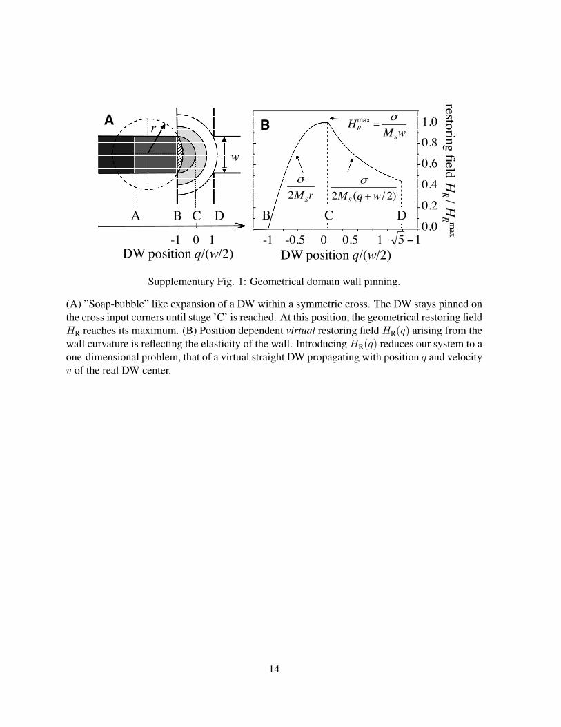
Supplementary Note 1:Elastic bubble expansion and geometrical pinning
To describe the geometrical DW pinning exploited in our experiment we employ a simple DW
propagation model where the motion of a DW of negligible width is determined by the competi-
tion between DW energy E = ·t · l and Zeeman energy EZ = 2MS ·HA ·t ·S. = 4pAK?
is the DW energy per unit area, MS, A, and K? are saturation magnetisation, exchange stiffness
and effective out-of-plane uniaxial anisotropy constants, respectively, l is the DW length, S is
the area of the reversed domain and t is the thickness of the magnetic layer. The ’friction’ of
DW motion generated by DW pinning on defects in the magnetic film is described in our model
by a coercive intrinsic propagation field HP which is considered to be everywhere the same. We
also neglect the effect of magnetic pseudo-charges generated by DW deformation, since the ra-
dius of curvature is much larger than the width of the DW in our micrometer wide Hall-crossbar
structures. We therefore consider magnetic field driven DW propagation to be governed only
by the competition between DW energy and Zeeman energy.
We first consider a circular-shaped domain of radius r expanding around a nucleation center
1
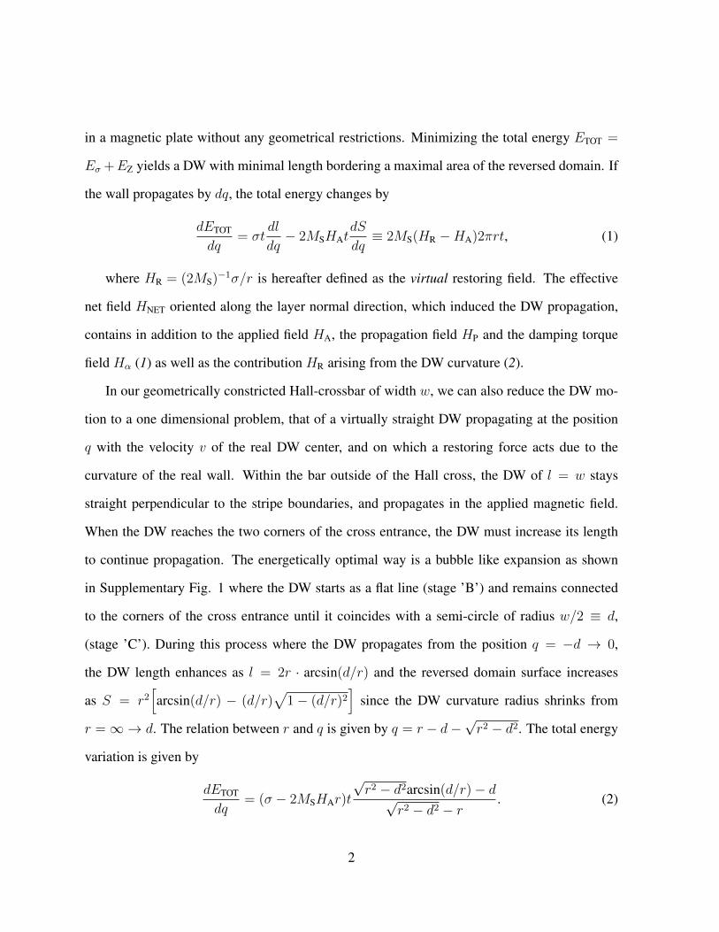
in a magnetic plate without any geometrical restrictions. Minimizing the total energy ETOT =
E +EZ yields a DW with minimal length bordering a maximal area of the reversed domain. If
the wall propagates by dq, the total energy changes by
dETOT
dq= t
dl
dq 2MSHAt
dS
dq 2MS(HR HA)2rt, (1)
where HR = (2MS)1/r is hereafter defined as the virtual restoring field. The effective
net field HNET oriented along the layer normal direction, which induced the DW propagation,
contains in addition to the applied field HA, the propagation field HP and the damping torque
field H↵ (1) as well as the contribution HR arising from the DW curvature (2).
In our geometrically constricted Hall-crossbar of width w, we can also reduce the DW mo-
tion to a one dimensional problem, that of a virtually straight DW propagating at the position
q with the velocity v of the real DW center, and on which a restoring force acts due to the
curvature of the real wall. Within the bar outside of the Hall cross, the DW of l = w stays
straight perpendicular to the stripe boundaries, and propagates in the applied magnetic field.
When the DW reaches the two corners of the cross entrance, the DW must increase its length
to continue propagation. The energetically optimal way is a bubble like expansion as shown
in Supplementary Fig. 1 where the DW starts as a flat line (stage ’B’) and remains connected
to the corners of the cross entrance until it coincides with a semi-circle of radius w/2 d,
(stage ’C’). During this process where the DW propagates from the position q = d ! 0,
the DW length enhances as l = 2r · arcsin(d/r) and the reversed domain surface increases
as S = r2harcsin(d/r) (d/r)
p1 (d/r)2
isince the DW curvature radius shrinks from
r = 1 ! d. The relation between r and q is given by q = r dpr2 d2. The total energy
variation is given by
dETOT
dq= ( 2MSHAr)t
pr2 d2arcsin(d/r) dp
r2 d2 r. (2)
2
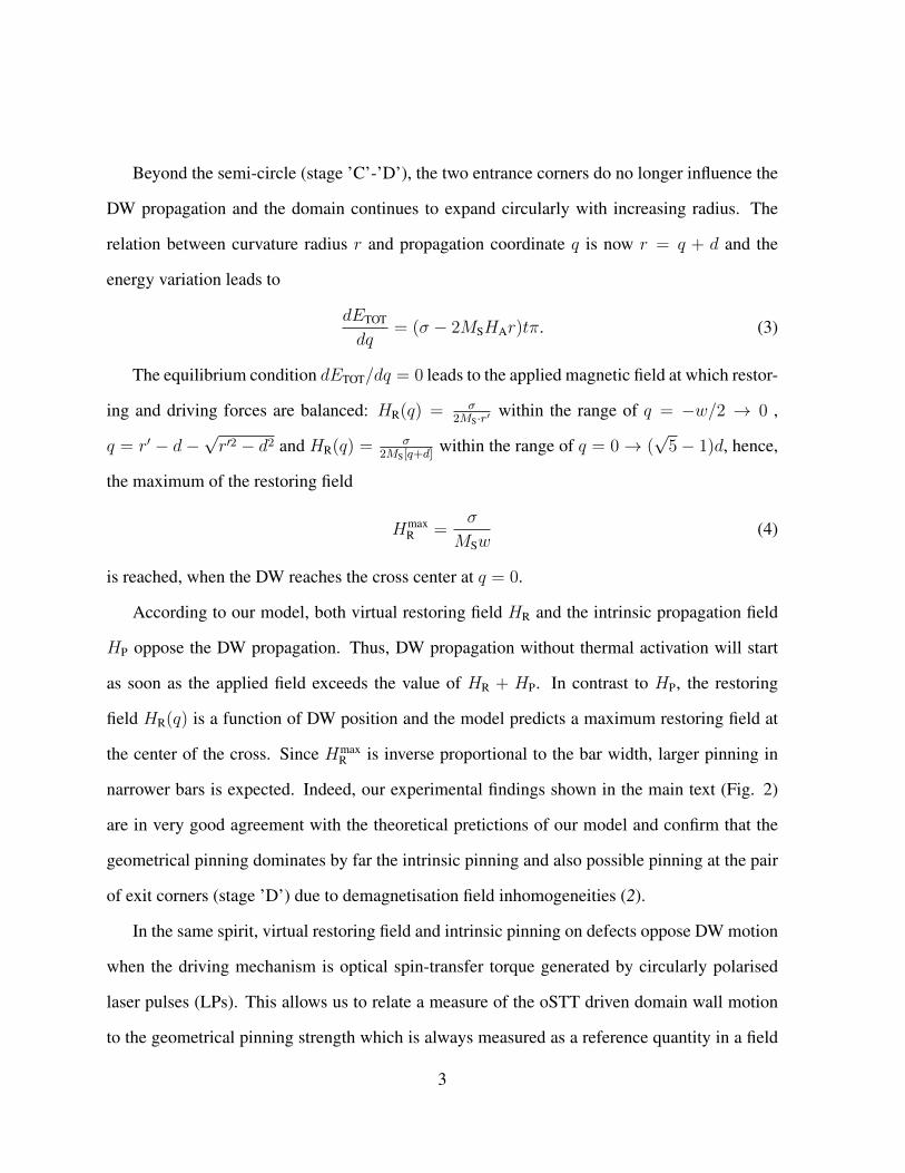
Beyond the semi-circle (stage ’C’-’D’), the two entrance corners do no longer influence the
DW propagation and the domain continues to expand circularly with increasing radius. The
relation between curvature radius r and propagation coordinate q is now r = q + d and the
energy variation leads to
dETOT
dq= ( 2MSHAr)t. (3)
The equilibrium condition dETOT/dq = 0 leads to the applied magnetic field at which restor-
ing and driving forces are balanced: HR(q) = 2MS·r0 within the range of q = w/2 ! 0 ,
q = r0 dpr02 d2 and HR(q) =
2MS[q+d] within the range of q = 0 ! (
p5 1)d, hence,
the maximum of the restoring field
HmaxR =
MSw(4)
is reached, when the DW reaches the cross center at q = 0.
According to our model, both virtual restoring field HR and the intrinsic propagation field
HP oppose the DW propagation. Thus, DW propagation without thermal activation will start
as soon as the applied field exceeds the value of HR + HP. In contrast to HP, the restoring
field HR(q) is a function of DW position and the model predicts a maximum restoring field at
the center of the cross. Since HmaxR is inverse proportional to the bar width, larger pinning in
narrower bars is expected. Indeed, our experimental findings shown in the main text (Fig. 2)
are in very good agreement with the theoretical pretictions of our model and confirm that the
geometrical pinning dominates by far the intrinsic pinning and also possible pinning at the pair
of exit corners (stage ’D’) due to demagnetisation field inhomogeneities (2).
In the same spirit, virtual restoring field and intrinsic pinning on defects oppose DW motion
when the driving mechanism is optical spin-transfer torque generated by circularly polarised
laser pulses (LPs). This allows us to relate a measure of the oSTT driven domain wall motion
to the geometrical pinning strength which is always measured as a reference quantity in a field
3

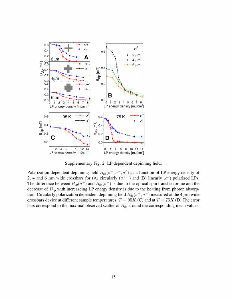
assisted depinning experiment without irradiation. In Supplementary Fig. 2, we present data
of polarisation dependent depinning fields Bdp of 2, 4 and 6 µm wide crossbar devices as a
function of LP energy density. Without laser irradiation, Bdp is largest for the narrowest bar.
Thermal heating by the LP irradiation, however, is more efficient for the narrower device so
that the reduction of Bdp is faster with increasing LP energy density for the narrower bars. We
performed experiments also at a higher and lower temperature, Supplementary Fig. 2 C,D. The
comparison of the 75K and 95K measurements, shown below, indeed confirms that oSTT is
present independently of the sample temperature. At lower temperatures, depinning without
additional applied magnetic field is realised at even lower laser powers.
Supplementary Note 2: Micromagnetic method
2.1: Landau-Lifshitz-Bloch approach (LLB)
We state again here firstly the governing equations as the forthcoming description is centered
around them: The time evolution of the magnetization m in the LLB approach (3) and the
spin-density s (4) read :
@m@t
= m Heff + tr + lt (5)
@s@t
=Jex
~meq
s m +R(t)n srec
(6)
We start by describing Eq.(5): There, m is the magnetization at temperature T , normalized
by the zero temperature saturation magnetization M0 , is the gyromagnetic ratio and Heff is
the effective field (as described later on). M0 was determined by extrapolation of SQUID-data
and is here 35.5 kA/m. The first term on the right hand-side of Eq. (1) describes the precession
of m around Heff while the second term tr=↵?m2 m (m Heff) is the transverse torque with
an associated damping ↵?(T )=1 T
3TC
, resulting in relaxation of m into the direction of
Heff. Here, is the microscopic damping parameter at T=0.
4
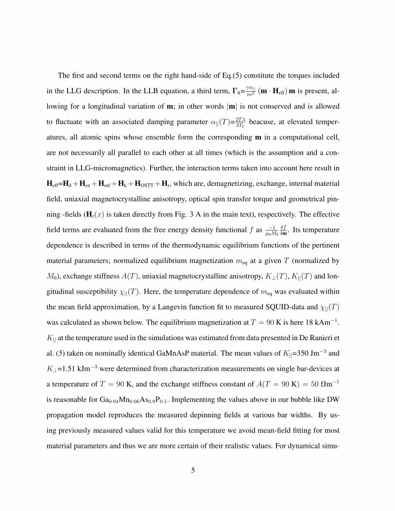
The first and second terms on the right hand-side of Eq.(5) constitute the torques included
in the LLG description. In the LLB equation, a third term, lt=↵||m2 (m · Heff)m is present, al-
lowing for a longitudinal variation of m; in other words |m| is not conserved and is allowed
to fluctuate with an associated damping parameter ↵||(T )=2T3TC
beacuse, at elevated temper-
atures, all atomic spins whose ensemble form the corresponding m in a computational cell,
are not necessarily all parallel to each other at all times (which is the assumption and a con-
straint in LLG-micromagnetics). Further, the interaction terms taken into account here result in
Heff=Hd+Hex+Hmf+Hk+HOSTT+Hr, which are, demagnetizing, exchange, internal material
field, uniaxial magnetocrystalline anisotropy, optical spin transfer torque and geometrical pin-
ning -fields (Hr(x) is taken directly from Fig. 3 A in the main text), respectively. The effective
field terms are evaluated from the free energy density functional f as 1µ0M0
fm . Its temperature
dependence is described in terms of the thermodynamic equilibrium functions of the pertinent
material parameters; normalized equilibrium magnetization meq at a given T (normalized by
M0), exchange stiffness A(T ), uniaxial magnetocrystalline anisotropy, K?(T ), K||(T ) and lon-
gitudinal susceptibility ||(T ). Here, the temperature dependence of meq was evaluated within
the mean field approximation, by a Langevin function fit to measured SQUID-data and ||(T )
was calculated as shown below. The equilibrium magnetization at T = 90 K is here 18 kAm1.
K|| at the temperature used in the simulations was estimated from data presented in De Ranieri et
al. (5) taken on nominally identical GaMnAsP material. The mean values of K||=350 Jm3 and
K?=1.51 kJm3 were determined from characterization measurements on single bar-devices at
a temperature of T = 90 K, and the exchange stiffness constant of A(T = 90 K) = 50 fJm1
is reasonable for Ga0.94Mn0.06As0.9P0.1. Implementing the values above in our bubble like DW
propagation model reproduces the measured depinning fields at various bar widths. By us-
ing previously measured values valid for this temperature we avoid mean-field fitting for most
material parameters and thus we are more certain of their realistic values. For dynamical simu-
5
lations we choose the damping parameter =0.01. All simulations are performed considering a
base temperature of T = 90 K (in accordance to most of the experimental measurements). The
demagnetizing field is divided into near-field and the far-field contributions and is described in
terms of the demagnetizing tensor, N in the standard manner; the dipole field at point ri from
all dipoles at points rj is Hid(T )=meqM0
Pj N(ri rj,x,y,z)mj, where x,y,z are the
dimensions of the discretization cells used along x, y and z, respectively. For the near-field, N
is evaluated by the analytical formulae for interactions between tetragonal cells as derived by
Newell, Williams and Dunlop (6). For the far-field (here, for inter-cell distances 40 cells ),
the kernel elements of N correspond to those for point dipoles. N need only to be computed
once and stored in memory. The form of Hid(T ) is that of a spatial convolution. This convo-
lution is then evaluated by standard FFT-techniques. The exchange field Hex(T )= 2A(T )µ0m2
eqM0@2
r m,
where the second derivative is computed by a finite difference three-point stencil in each spa-
tial direction. Hmf, responsible for stabilizing |m| is determined by the parallel susceptibility
||(T ) as Hmf(T )= 12||(T )
1 m2
m2eq
m with || = (@meq/@H)H!0 and H being the magnitude
of an applied field. In this work, the global easy axis u||z and the in-plane uniaxial anisotropy
axis u||y. Each anisotropy term contributes to Hk(T ) as Hk(T )= 2K(T )µ0m2
eq(T )M0(m · u)u. The last
effective field term, Hr(T ) is based on the considered pinning field profile for a bubble domain
pinned at a cross, while the effect of temperature is taken into account by considering the re-
duction of |Bdp| for 0-light at the laser fluency corresponding to DW depinning for +-light.
Therefore, the maximum |Hr(T )| used in the simulation corresponds to 0.1 mT. As it acts as
to pull the DW in the opposite direction of its excited motion, then in the simulations, the di-
rection of the virtual restoring field Hr(x) is along the z-direction if the DW moves along the
±x-direction. Finally, the boundary condition used for m on all free surfaces is @m@rn
= 0, where
rn is the outward unit normal.
We now turn to Eq.(6) and its coupling to Eq.(5). Here, Jex is the exchange coupling between
6
photo-induced electrons and the local magnetization m. We use Jex=JSMncMn, where J=10
meVnm3, SMn=5/2 is the local Mn-moment and cMn 1 nm3 is the typical moment density
(?). When coupling to the LLB-equation we assume a temperature variation of the effective
exchange coupling to the macro-vector m at increased T and for simplicity assume Jex !
Jexm2eq. The first term on the right hand-side of Eq.(6) describes the precession of s around the
exchange field produced by m (in this step the effect of m on s is established) while the second
term gives the injection of spin-polarized electrons with R being the rate per unit volume and n
the initial spin polarization direction defined by the helicity of the light with n=[00±1]. Finally,
the third term represents the decay of the photo-carrier spin with a life-time of rec, limited in
our case by the carrier-recombination time. Based on previous measurements in literature, we
set rec=30 ps. Gradient terms in s are neglected. During precession, s transfer its angular
momentum to m. The precession time of s is very fast as compared to the natural precession of
m ( 100 fs versus 1 ns). The absorption of angular momentum from s results in a torque on
m. This torque is then entered into Eq.(5) by an augmentation to the rest of the effective field by
HOSTT (thus the effect of s on m is established); The interaction energy density between s and m
is fex=Jeff(T )meq
s · m. The corresponding effective field term is then according to the definition in
the preceeding paragraph, HOSTT(T )= Jeff(T )µ0meqM0
s. Equations (1) and (2) are solved together using
a 5th order Runge-Kutta integration scheme.
2.2: Computational geometry and simulation procedure
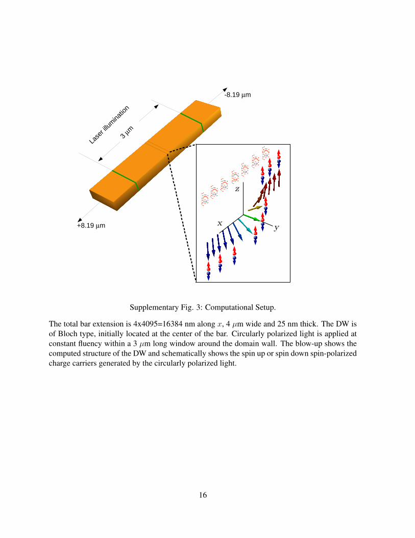
We consider a one-dimensional bar with 4095 x 1 x 1 computational cells composing a structure
as shown in Supplementary Fig. 3. The cell dimension is 4 nm x 4 µm x 25 nm. A Bloch DW is
initialized in the center of the bar and let to relax quickly with strong damping by setting =0.9.
This configuration is then used as a starting configuration for the simulations of domain wall
motion under the light pulses.
7
Once the domain wall is prepared, circularly polarized light is pulsed at a rate of 80 MHz.
The length of each pulse is set to 150 fs. For the simulation of the depinning process, the
spin-polarized carrier injection rate is R = 1.225 1039m3s1. This order of magnitude for
R is required for the DW to escape the elastic pinning potential. The equivalent pulse power
corresponds to the time-averaged laser power used in the experiments of the order of 20 mW
assuming a skin depth of 1 µm. Further, all simulations were done in zero externally applied
magnetic field and a damping of = 0.01 was used in all dynamical simulations.
Throughout all simulations a centering procedure is employed, that keeps the DW in the
middle of the length of the bar. In this way, propagation distances as long as needed can be
simulated without having to worry about stray field effects should the domain wall have come
close to the edges of the bar or that the DW moves out of the computational region.
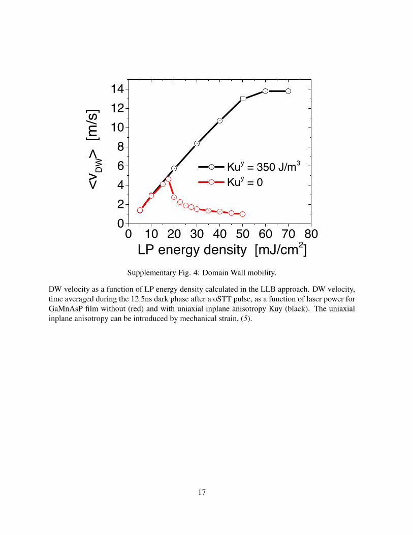
Supplementary Fig. 4 shows the calculated time-averaged DW velocity vDW as a function
of LP energy density. We identify the Walker breakdown peak velocity of about 5 m/s at about
18 mJ/cm2 for the DW with only out-of-plane magnetic anisotropy. Stabilising the DW struc-
ture, e.g., by DMI or by introducing additional anisotropy via mechanical strain, can shift the
WB to higher values and allow for achieving higher DW velocities, (5). We show in Supple-
mentary Fig. 4 that indeed higher velocities can be achieved when the static structure of the
DW is stabilised by introducing additional uniaxial in-plane anisotropy. We finally note that the
limiting speed for any texture to propagate in a given magnetic material is the magnon group
velocity vm. We estimate vm = 4 · J · SMn · a/~ using the parameter of our GaMnAsP film at
T = 90 K, a is the spin separation length and J is the next neighbour exchange constant. With
Jex = A · a/(2S2Mn) and a = (2 · g · µB · SMn/MS)1/3 (g is the Lande factor and µB is the Bohr
magneton) we obtain vm 1 km/s.
8
Supplementary Note 3:Additional experimental evidences for optical spin transfer torquedriven DW motion
3.1: Wavelength dependency of helicity dependent DW motion
We have performed wavelength dependent experiments to support the optical spin transfer
torque origin of the helicity dependent LP induced DW motion. In experiments described in
the main text we use LP excitation with a wavelength = 750 nm that excites photo-electrons
slightly above the bottom of the GaAs conduction band so that for a circularly polarized inci-
dent light, photo-electrons become spin-polarized with the degree of polarization approaching
the maximum theoretical value of 50% (7). At energies above and below band gap energy (Sup-
plementary Fig. 5), the spin polarisation of the photo-electrons is reduced. Photons excitation
at higher energies results in the reduction of net-photoelectron spin-polarisation mainly because
carrier excitation from the split-off valence band can take place. The photocarrier generation
from low-energy photons with sub-band gap energies comes mainly from excitation of impurity
states within the band gap.
3.2: Dependency of helicity dependent DW motion on the sweep directionof the focused laser spot
We now investigate the effect of the thermal gradients generated by the laser spot on the helicity
dependent DW depinning. By inverting the sweep direction of the focused LP spot with respect
to the geometrically pinned DW, we invert also the thermal gradient affecting the DW. In case
that the LP spot approaches from the reversed domain along the patterned bar, Supplementary
Fig. 6A, both Bdp(+) and Bdp() decrease faster compared to the situation where the laser
spot approaches from the unreversed domain (Supplementary Fig. 6B). This observation is
explained by the stronger temperature increase from LP heating in the narrow bar compared to
9
the lower temperature rise in the wider cross area. On the other hand, the helicity dependence
of Bdp, which is of oSTT origin, remains unaffected by the LP sweep direction.
3.3: Continuous wave excitation vs. laser pulse excitation
We now show that the DW can be also moved by a focused laser spot of continuous wave (cw)
excitation. To compare the efficiency of the cw-excitation with our ultrashort LP-excitation ap-
proach we have deduced Bdp(+) and Bdp() for LP- and cw-excitation at the same averaged
laser power Pav. Based on our LLB approach, we also have calculated DW propagation driven
by oSTT from LP- and cw- excitations. From the simulations, we have derived the averaged
DW velocity vs. Pav at the position of maximal restoring field (Supplementary Fig. 7A). Posi-
tive averaged velocities correspond therefore to the depinning of the DW. For zero or negative
velocities, the DW remains pinned. Both calculation and experimental results presented in Sup-
plementary Fig. 7 confirm that a DW can be depinned via oSTT generated by ultrashort LP
and by cw-excitation. However, cw-driven DW propagation requires always higher averaged
laser power (Supplementary Fig. 7A). Comparing Bdp(, +) (Supplementary Fig. 7B, C)
for the two excitation schemes at equal averaged laser power shows a stronger efficiency of
the pulsed oSTT. Moreover, the effect of laser heating on DW depinning is stronger in case
of cw-excitation compared to ultrashort LP-excitation. Therefore, helicity dependent inertial
DW motion induced by ultrashort LP is more efficient than DW motion induced by constant
excitation.
3.4: Temperature dependent depinning field
The temperature dependence of the resistance of the magnetic bar is used to monitor and control
the actual sample temperature (Supplementary Fig. 8A). In order to obtain the accurate resistiv-
ity dependence of our devices we performed a reference measurement in a bath cryostat, where
10
the (Ga,Mn)(As,P) sample is thermally anchored to a calibrated temperature sensor and where
the temperature dependent resistivity R(T ) of (Ga,Mn)(As,P) is monitored during heating-up
from 4 K to room temperature. The Curie temperature Tc = 115 K is obtained by identify-
ing the cusp in dR/dT (8), (Supplementary Fig. 8A). We have determined Bdp without laser
irradiation at a 4 µm wide device as a function of temperature in a temperature range below
T = 90 K until close to Curie-temperture (Supplementary Fig. 8B). This allows us to estimate
an effective sample temperature deduced from the comparison between temperature dependent
measurements of Bdp without irradiation and measurements of Bdp(0) vs. Pav laser power and
at fixed base temperature (9).
3.5: MCD induced temperature gradients
In this section, we identify the sign and estimate the magnitude of the temperature gradient gen-
erated by MCD between two opposite magnetized domains. We use a 6 µm wide, 18 µm long
(contact-to-contact) bar-device patterned from our GaMnAsP/GaAs film. LPs are focused at
the center of our bar as shown in Supplementary Fig. 9. We evaluate the temperature variation
at opposite saturation magnetisations from the resistance variation detected in our sample at
fixed LP polarisation. We employ a sensitive double Lock-in technique and compare magneti-
sation dependent resistance variation with the temperature dependence of the GaMnAsP film
resistivity.
To estimate the temperature variation at the irradiated spot position from the resistance
variation measured in 4-point geometry over the whole bar device, we employ a simple re-
sistor network model described in Supplementary Fig. 10. The 18 µm long and 6 µm wide
bar is divided into 27 (2 µm 2 µm) squares. Only the central square is irradiated hav-
ing the resistance RLsq . All other squares remain in darkness having the equal resistances,
RDsq. Within this simple resistor network model, we can estimate the temperature variations
11
generated by the MCD at the irradiated square of the device by detecting the total device re-
sistance variation at opposite saturation magnetisations when comparing the measured data to
a reference measurement of the temperature dependency of = R(T )/R(90 K), Supple-
mentary Fig. 10, right. Since only the irradiated spot can be compared with this reference
measurement, we need to relate the sample temperature variation of the spot to the measur-
able resistance variation of the total device as shown in Supplementary Fig. 10 (left). In the
frame of this approximation, the ratio of irradiated and non-irradiated square resistances is
estimated to = RLsq/R
Dsq = 27RL
T/RDT 26; (RL
T , and RDT are the measurable total bar
device resistances with and without spot irradiation). To avoid any small alternations of our
focused LP spot in intensity, spot position, etc., we measure the resistance variation due to
the MCD by changing periodically the sample saturation magnetisation (at a frequency of 0.2
Hz) and keeping simultaneously the LP polarisation fixed. A first Lock-in amplifier measures
the 4-point resistance as the response to an alternating probe current (f = 123 Hz). After the
subtraction of an offset, the output of the first Lock-in is amplified by a factor x100. The re-
sulting signal feeds into a second Lock-in, which amplifies the signal with reference to the
alternating saturation magnetisation. As a result, we obtain Rm = RLT,+Mz
RLT,Mz
. We
evaluate dT = T (RLsq,+Mz
) T (RLsq,Mz
) = ↵(+Mz Mz), with T = ↵ and ↵ is ob-
tained from the linear slope of the temperature dependence of the sample resistance around
T = 90 K. Since +Mz Mz = 27(RLT,+Mz
RLT,Mz
)/RDT = 27Rm/R
DT , we can estimate
dT = 27↵Rm/RDT with RD
T = 1.244 k.
In Supplementary Fig. 11(a,b) we show the LP polarisation dependent temperature variation
at the irradiated spot between positive and negative saturation magnetisations. At T = 90 K
substrate temperature, the temperature variation is of the order of +()200 mK for circularly
polarised +() LPs. Hence, the +() LPs irradiated film with positive (negative) magneti-
sation becomes hotter than the film with negative (positive) magnetisation orientation.
12
In our oSTT experiments shown in Fig. 3 of the main text, we saturate the magnetic bar in
a strong negative magnetic field and nucleate a reversed domain at the left side of the bar with
positive magnetisation orientation . When irradiated with +() polarised LPs, MCD heats up
the nucleated magnetic domain more (less) than the rest of the magnetic film with negative mag-
netization orientation. In the experiment, we observe DW depinning and motion towards the
area with negative magnetisation only when the DW is irradiated with + polarised LPs. If we
repeat the experiment with inverted magnetisation (positive saturation, nucleated domain with
negative magnetisation orientation) the DW moves towards the positive magnetisation orienta-
tion only when irradiated with polarised LPs. Hence, we always observe that the circularly
polarised LP exposed DW moves towards the colder region, which excludes the MCD origin
of the observed DW motion. Considering a DW width of 50 nm (Supplementary Fig. 11C),
we estimate a MCD generated heat gradient of 6 106 K/m. This value is smaller than the
heat-gradient generated by the focused light spot independent of polarisation.
13
w
σ σ
wMH
SR
σ=max
r 1.0
0.8
0.6
restoring fieldA B
A B C D
-1 0 1 -1 -0.5 0 0.5 1 15 −
rMS2σ
)2/(2 wqMS +σ
B C D
DW position q/(w/2) DW position q/(w/2)
0.4
0.2
0.0
HR / H
R max
Supplementary Fig. 1: Geometrical domain wall pinning.
(A) ”Soap-bubble” like expansion of a DW within a symmetric cross. The DW stays pinned onthe cross input corners until stage ’C’ is reached. At this position, the geometrical restoring fieldHR reaches its maximum. (B) Position dependent virtual restoring field HR(q) arising from thewall curvature is reflecting the elasticity of the wall. Introducing HR(q) reduces our system to aone-dimensional problem, that of a virtual straight DW propagating with position q and velocityv of the real DW center.
14
2µm
4µm
6µm
0.0
0.2
0.4
0.6 σ+ σ-
B dp
[mT]
0.2
0.4
0.6 σ+ σ-
0.0
0.2
0.4
0.6
σ+ σ-
0.2
0.4
0.6σ0
B dp
[mT]
2 µm 4 µm 6 µm
A
B6µm0 1 2 3 4 5 6 7 8
0.0
LP energy density [mJ/cm2]0 1 2 3 4 5 6 7 8
0.0
LP energy density [mJ/cm2]
0 2 4 6 8 10 12 14
0.0
0.2
0.4
0.6
B dp
[mT]
LP energy density [mJ/cm2]
σ+
σ-
0 2 4 6 8 10 12 14
0.0
0.2
0.4
0.6
B dp
[mT]
LP energy density [mJ/cm2]
σ+
σ-95 K 75 K
C D
Supplementary Fig. 2: LP dependent depinning field.
Polarization dependent depinning field Bdp(+, , 0) as a function of LP energy density of2, 4 and 6 µm wide crossbars for (A) circularly (+,) and (B) linearly (0) polarized LPs.The difference between Bdp(+) and Bdp() is due to the optical spin transfer torque and thedecrease of Bdp with increaseing LP energy density is due to the heating from photon absorp-tion. Circularly polarization dependent depinning field Bdp(+, ) measured at the 4 µm widecrossbars device at different sample temperatures, T = 95K (C) and at T = 75K (D) The errorbars correspond to the maximal observed scatter of Bdp around the corresponding mean values.
15
+8.19 µm
-8.19 µm
yx
z
Lase
r illum
inatio
n
3 µm
Supplementary Fig. 3: Computational Setup.
The total bar extension is 4x4095=16384 nm along x, 4 µm wide and 25 nm thick. The DW isof Bloch type, initially located at the center of the bar. Circularly polarized light is applied atconstant fluency within a 3 µm long window around the domain wall. The blow-up shows thecomputed structure of the DW and schematically shows the spin up or spin down spin-polarizedcharge carriers generated by the circularly polarized light.
16
68
101214
Kuy = 350 J/m3
K y 0v DW
> [m
/s]
0 10 20 30 40 50 60 70 80024 Kuy = 0
LP energy density [mJ/cm2]
<v
Supplementary Fig. 4: Domain Wall mobility.
DW velocity as a function of LP energy density calculated in the LLB approach. DW velocity,time averaged during the 12.5ns dark phase after a oSTT pulse, as a function of laser power forGaMnAsP film without (red) and with uniaxial inplane anisotropy Kuy (black). The uniaxialinplane anisotropy can be introduced by mechanical strain, (5).
17
750 nm 700 nm 600 nm
0.0
0.1
0.2
0.3
0.4
0.5
0.6 880 nm
0.0
0.1
0.2
0.3
A
900 850 800 750 700 650 600
0.0
0.1
0.2
wavelength (nm)
0 5 10 15-0.1
0 5 10 15 0 5 10 15 0 5 10 15laser pulse energy density (mJ/cm2)
900 850 800 750 700 650 6000.0
0.1
0.2
0.3
0.4
wavelength (nm)
Wavelength dependency @ 7 mJ/cm2 B
Supplementary Fig. 5: Wavelength dependent domain wall depinning.
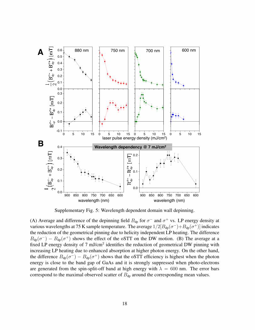
(A) Average and difference of the depinning field Bdp for and + vs. LP energy density atvarious wavelengths at 75 K sample temperature. The average 1/2[Bdp()+Bdp(+)] indicatesthe reduction of the geometrical pinning due to helicity independent LP heating. The differenceBdp() Bdp(+) shows the effect of the oSTT on the DW motion. (B) The average at afixed LP energy density of 7 mJ/cm2 identifies the reduction of geometrical DW pinning withincreasing LP heating due to enhanced absorption at higher photon energy. On the other hand,the difference Bdp() Bdp(+) shows that the oSTT efficiency is highest when the photonenergy is close to the band gap of GaAs and it is strongly suppressed when photo-electronsare generated from the spin-split-off band at high energy with = 600 nm. The error barscorrespond to the maximal observed scatter of Bdp around the corresponding mean values.
18
Laser spotshift-trajectory
initially pinned DW
Laser spotshift-trajectory
initially pinned DW
0.4
T]
σ+ σ-
σ+ σ-
A B
0 2 4 6 8 100.0
0.2
B dp
[mT
LP energy density [mJ/cm2]
0 2 4 6 8 10
LP energy density [mJ/cm2]
Supplementary Fig. 6: Sweep direction dependent domain wall depinning.
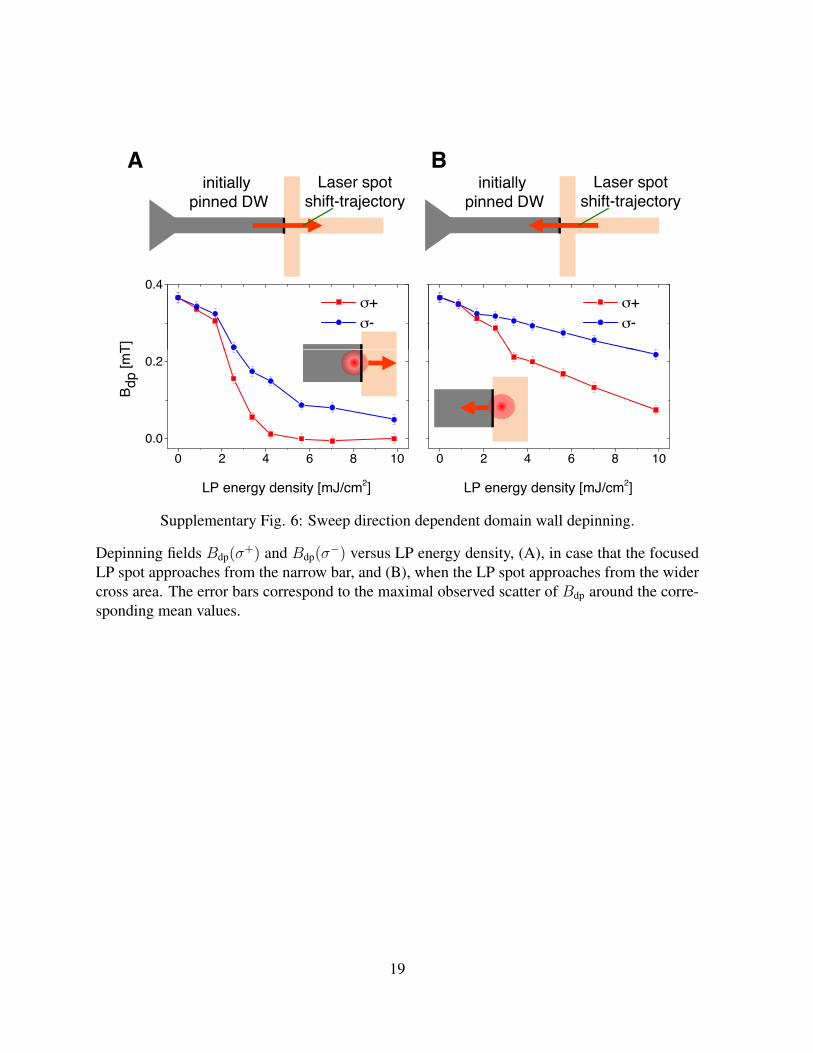
Depinning fields Bdp(+) and Bdp() versus LP energy density, (A), in case that the focusedLP spot approaches from the narrow bar, and (B), when the LP spot approaches from the widercross area. The error bars correspond to the maximal observed scatter of Bdp around the corre-sponding mean values.
19
0 5 10 15 20 250.0
0.1
0.2
0.3
0.4
B d (m
T)
Pav (mW)
σ+
σ0
σ-
LASER PULSES
90 95 100 105T (K)
15 20 25 30 35 40 45-4
-2
0
2
4
6LLB SIMULATION
Pav (mW)
<v> D
W (m
/s) continuous
pulses
0 5 10 15 20 250.0
0.1
0.2
0.3
0.4
σ+
σ0
σ-
CONTINUOUS
Pav (mW)
B d (m
T)
90 95 100 105 110 115 120T (K)
A B C
Supplementary Fig. 7: Ultrashort pulse excitation vs. continuous cw laser excitation
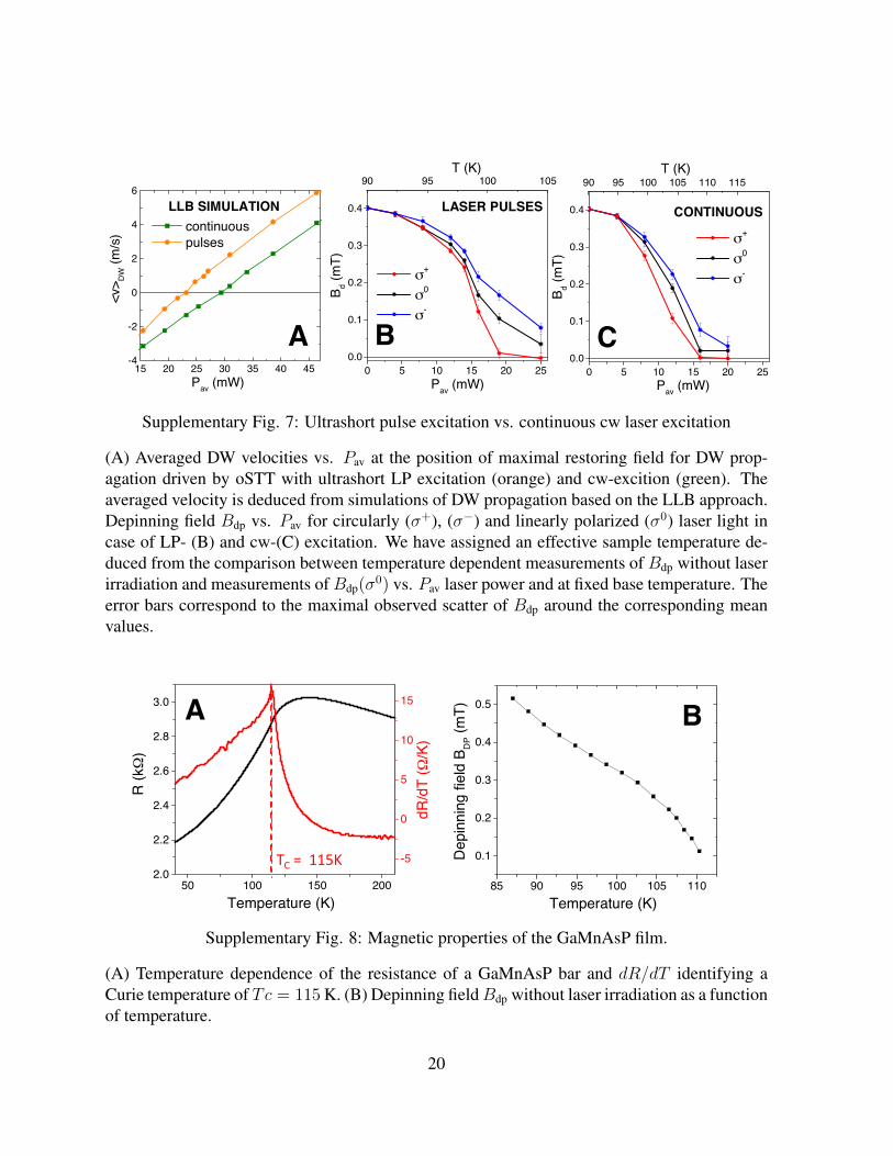
(A) Averaged DW velocities vs. Pav at the position of maximal restoring field for DW prop-agation driven by oSTT with ultrashort LP excitation (orange) and cw-excition (green). Theaveraged velocity is deduced from simulations of DW propagation based on the LLB approach.Depinning field Bdp vs. Pav for circularly (+), () and linearly polarized (0) laser light incase of LP- (B) and cw-(C) excitation. We have assigned an effective sample temperature de-duced from the comparison between temperature dependent measurements of Bdp without laserirradiation and measurements of Bdp(0) vs. Pav laser power and at fixed base temperature. Theerror bars correspond to the maximal observed scatter of Bdp around the corresponding meanvalues.
85 90 95 100 105 110
0.1
0.2
0.3
0.4
0.5
Temperature (K)
Dep
inni
ng fi
eld
B DP (
mT)
50 100 150 2002.0
2.2
2.4
2.6
2.8
3.0
R (k
Ω)
Temperature (K)
-5
0
5
10
15
dR/d
T (Ω
/K)
TC = 115K
A B
Supplementary Fig. 8: Magnetic properties of the GaMnAsP film.
(A) Temperature dependence of the resistance of a GaMnAsP bar and dR/dT identifying aCurie temperature of Tc = 115 K. (B) Depinning field Bdp without laser irradiation as a functionof temperature.
20
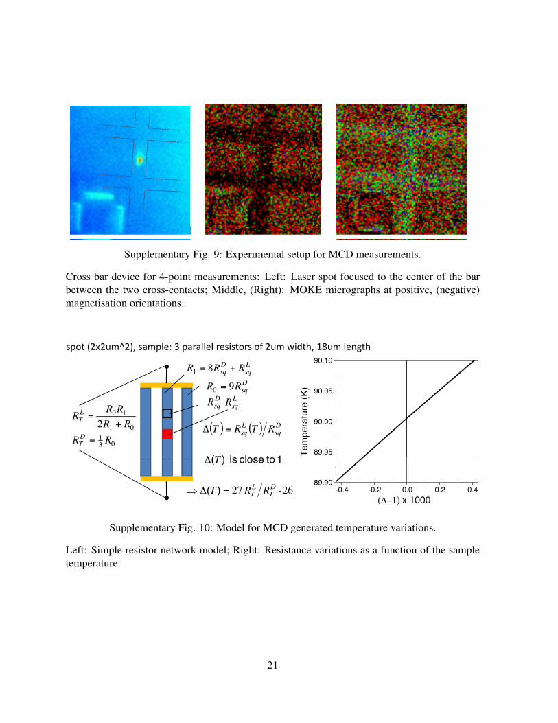
Supplementary Fig. 9: Experimental setup for MCD measurements.
Cross bar device for 4-point measurements: Left: Laser spot focused to the center of the barbetween the two cross-contacts; Middle, (Right): MOKE micrographs at positive, (negative)magnetisation orientations.
DsqRR 90 =
Lsq
Dsq RRR += 81
LsqRD
sqR
01
10
2 RRRRRL
T +=
( ) ( ) Dsq
Lsq RTRT ≡∆
1tli)(T∆
031 RRD
T =89.95
90.00
90.05
90.10
Tem
pera
ture
(K)
spot (2x2um^2), sample: 3 parallel resistors of 2um width, 18um length
1 to close is )( T∆
)( 2627 -RRT DT
LT=∆⇒
89.90-0.4 -0.2 0.0 0.2 0.4
(∆−1) x 1000
Supplementary Fig. 10: Model for MCD generated temperature variations.
Left: Simple resistor network model; Right: Resistance variations as a function of the sampletemperature.
21
0 90 180 270 360
-0.15
0.00
0.15
∆T
[K]
φ (λ/4-waveplate rotation angle) [deg]
σ+ σ-(a)
300
450
(σ+ − σ−)
[mK
]
75K 90K 117K
(b)
φ (λ/4-waveplate rotation angle) [deg]
(c)
0.0 5.0 10.0 15.0
0
150
LP energy density [mJ/cm2]
∆T
(
Supplementary Fig. 10: MCD induced temperature variations.
(a): Temperature variation measured at T = 90 K substrate temperature and for a laser powerof 10 mJ/cm2 as a function of LP polarisation. The polarisation is varied by a /4-waveplate.A constant offset is subtracted from all data points. Before taking a data point, we alwaysrealigned the focused laser spot to the bar center. The discrepancy between the measured an-gular dependence of the temperature variation from the expected cos(2) behaviour is due tounintentional polarisation effects in some of the optical components in our setup. + and
polarised LPs correspond to = 135 deg and = 195 deg, respectively. As expected for MCDrelated heating, we find largest temperature variations for + (red line) and for (blue line)polarisations. (b) MCD induced differences in temperature variation between + and as afunction of LP energy density for 3 different substrate temperatures, 75 K (blue), 90 K (green),and 117 K (red). Note that the MCD induced heating disappears above the Curie tempera-ture TC =115 K. The error bars correspond to the standard deviation of the detected resistancevariation. (c) Static DW profiles obtained by micromagnetic simulation with 0.5 nm (2 nm)discretisation length along (perp. to) a 4 µm wide bar. The simulation is based on the exper-imentally obtained values at T =90 K for out-of-plane uniaxial anisotropy K? =1500 Jm3,saturation magnetization MS =18.2 kA/m and we use A =50 fJ/m for the exchange stiffnessparameter.
22
Supplementary References
1. A. P. Malozemoff, J. C. Slonczewski: Magnetic Domain Walls in Bubble Materials, Aca-
demic Press, New York (1979).
2. J. Wunderlich: Extraordinary Hall Effect in Multi-layered Magnetic Films: Application to
the Study of Magnetization Reversal Dynamics, ISBN-13: 978-3826591105, Shaker Verlag,
Germany (2001).
3. C. Schieback, et al., Temperature dependence of the current-induced domain wall motion
from a modified Landau-Lifshitz-Bloch equation, Phys. Rev. B. 80, 214403 (2009).
4. P. Nemec, et al., Experimental observation of the optical spin transfer torque, Nat. Phys. 8,
411 - 415 (2012).
5. E. De Ranieri, et al., Piezoelectric control of the mobility of a domain wall driven by adia-
batic and non-adiabatic torques, Nat. Mater. 12, 808 - 814 (2013).
6. A. J. Newell, W. Williams, D. J., Dunlop, A generalization of the demagnetizing tensor for
nonuniform magnetization, J. Geophys. Res., 98 9551-9555 (1993).
7. G. E. Pikus, A. N. Titkov, in Optical Orientation, F. Meier, B. P. Zakharchenya, Eds.
(North-Holland, Amsterdam, 1984), p. 73.
8. V. Novak, et al., Curie Point Singularity in the Temperature Derivative of Resistivity in
(Ga,Mn)As, Phys. Rev. Lett. 101, 077201 (2008).
9. S. Shihab, et al., Steady-state thermal gradient induced by pulsed laser excitation in a ferro-
magnetic layer, J. Appl. Phys. 119, 153904 (2016).
23