Industrial Voltage and Current Output Driver, Isolated ... · PDF fileimmunity to the...
24
An IMPORTANT NOTICE at the end of this TI reference design addresses authorized use, intellectual property matters and other important disclaimers and information. TINA-TI is a trademark of Texas Instruments WEBENCH is a registered trademark of Texas Instruments TIDU011-December 2013-Revised December 2013 Industrial Voltage and Current Output Driver, Isolated, EMC/EMI Tested 1 Copyright © 2013, Texas Instruments Incorporated Kevin Duke, Collin Wells TI Precision Designs: CerTIfied Design Single-Channel Industrial Voltage and Current Output Driver, Isolated, EMC/EMI Tested TI Precision Designs Circuit Description TI Precision Designs are analog solutions created by TI’s analog experts. CerTIfied Designs offer the theory, component selection, simulation, complete PCB schematic & layout, bill of materials, measured performance, and certification testing results of useful circuits. Circuit modifications that help to meet alternate design goals are also discussed. This single-channel analog output module delivers voltage and current outputs using the fully integrated DAC8760 analog front-end. The analog output module is galvanically isolated from the host controller with the ISO7641 digital isolator. Additionally, an external protection circuit is implemented to provide immunity to the IEC61000-4 suite of tests. Design Resources Design Archive All Design files TINA-TI™ SPICE Simulator DAC8760 Product Folder ISO7641 Product Folder Ask The Analog Experts WEBENCH® Design Center TI Precision Designs Library Isolation Barrier Field Connections DVDD DVDD-EN AVDD LATCH SCLK SDIN SDO GND HART IN DAC8760 AVSS REFIN REFOUT +VSENSE VOUT -VSENSE CMP IOUT GND VDD SCLK MOSI MISO /CS Digital Controller ISO7641 OUTA OUTB OUTC GND2 VCC2 INA INB INC GND1 VCC1 OUTD IND +15V -15V 100nF 15Ω Current Output 0-20mA, 4-20mA, 0-24mA 0-5V, 0-10V, ±5V, ±10V Voltage Output +15V -15V Ferrite Bead 15Ω 15Ω 1nF 0.1mF 22nF +15V -15V 0.1mF 100pF 0.1mF 100pF 0.1mF 0.1mF 0.1mF 0.1mF 15V Bidirectional TVS 15V Bidirectional TVS 100nF
Transcript of Industrial Voltage and Current Output Driver, Isolated ... · PDF fileimmunity to the...
An IMPORTANT NOTICE at the end of this TI reference design addresses authorized use, intellectual property matters and other important disclaimers and information.
TINA-TI is a trademark of Texas Instruments WEBENCH is a registered trademark of Texas Instruments
TIDU011-December 2013-Revised December 2013 Industrial Voltage and Current Output Driver, Isolated, EMC/EMI Tested 1 Copyright © 2013, Texas Instruments Incorporated
Kevin Duke, Collin Wells
TI Precision Designs: CerTIfied Design
Single-Channel Industrial Voltage and Current Output Driver, Isolated, EMC/EMI Tested
TI Precision Designs Circuit Description
TI Precision Designs are analog solutions created by TI’s analog experts. CerTIfied Designs offer the theory, component selection, simulation, complete PCB schematic & layout, bill of materials, measured performance, and certification testing results of useful circuits. Circuit modifications that help to meet alternate design goals are also discussed.
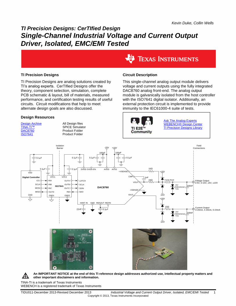
This single-channel analog output module delivers voltage and current outputs using the fully integrated DAC8760 analog front-end. The analog output module is galvanically isolated from the host controller with the ISO7641 digital isolator. Additionally, an external protection circuit is implemented to provide immunity to the IEC61000-4 suite of tests.
Design Resources
Design Archive All Design files TINA-TI™ SPICE Simulator DAC8760 Product Folder ISO7641 Product Folder
Ask The Analog Experts WEBENCH® Design Center TI Precision Designs Library
Isolation
Barrier
Field
Connections
DVDD DVDD-EN AVDD
LATCH
SCLK
SDIN
SDO
GNDHART IN
DAC8760
AVSS
REFINREFOUT
+VSENSE
VOUT
-VSENSE
CMP
IOUTGND
VDD
SCLK
MOSI
MISO
/CS
Digital Controller
ISO7641
OUTA
OUTB
OUTC
GND2
VCC2
INA
INB
INC
GND1
VCC1
OUTD IND
+15V
-15V
100nF
15Ω Current Output0-20mA, 4-20mA, 0-24mA
0-5V, 0-10V, ±5V, ±10V Voltage Output
+15V
-15V
Ferrite Bead15Ω
15Ω
1nF
0.1mF22nF
+15V-15V
0.1mF
100pF
0.1mF
100pF
0.1mF
0.1mF0.1mF
0.1mF
15V
Bidirectional
TVS
15V
Bidirectional
TVS
100nF

www.ti.com
2 Industrial Voltage and Current Output Driver, Isolated, EMC/EMI Tested TIDU011-December 2013-Revised December 2013 Copyright © 2013, Texas Instruments Incorporated
1 Design Summary
The design requirements are as follows:
Supply Voltage: ±15 V
Input: 4-wire SPI
Voltage Output: ±10 V
Current Output: 0 mA – 24 mA
The goals for this design are to provide immunity to the IEC-61000-4 suite of tests with minimum impact on the performance of the DAC8760 in an analog output module application. The specific design goals and performance are summarized in Table 1. Figure 1 depicts the measured transfer function of the design.
Table 1. Comparison of Design Goals, Simulation, and Measured Performance
Goal Calculated Measured
Voltage Output Total Unadjusted Error (%FSR)
0.1% 0.03 0.014
Current Output Total Unadjusted Error (%FSR)
0.1% 0.08 0.042
IEC61000-4 Immunity Pass n/a Pass
Figure 1: Measured Transfer Function
0
4
8
12
16
20
24
0 20000 40000 60000
Ou
tput C
urr
en
t (m
A)
Input Code
0-24 mA
C004
Warning! Do not move, alter, violate, or delete red bounding box or this warning!
Warning! Do not move, alter, violate, or delete red bounding box or this warning!
-10
-8
-6
-4
-2
0
2
4
6
8
10
0 20000 40000 60000
Ou
tpu
t V
olta
ge
(V
)
Input Code
+/-10 V
C004
Warning! Do not move, alter, violate, or delete red bounding box or this warning!
Warning! Do not move, alter, violate, or delete red bounding box or this warning!
65535 65535
www.ti.com
TIDU011-December 2013-Revised December 2013 Industrial Voltage and Current Output Driver, Isolated, EMC/EMI Tested 3 Copyright © 2013, Texas Instruments Incorporated
2 Theory of Operation
2.1 Analog Front End
Figure 2 depicts a simplified version of the circuitry inside the DAC8760 used to deliver the voltage and current outputs common for analog output modules. A similar scheme could be used to implement a discrete solution. A 5 V digital-to-analog converter (DAC) drives the inputs for both the voltage (VOUT) and current (IOUT) output stages. The DAC uses an accurate, low-drift reference voltage (VREF) for strong dc performance. A 5 V regulator is included internally to generate the digital supply voltage, DVDD, for the isolated side of the system.
Simplified DAC8760 Output Block Diagram
VOUT
Range
Scaling
RF
DAC
AVDD
RSET
Q1
Q2
+
+
VREF
+
A3
RS2 RS3
RG1
RG2
AVDD
AVSS
AVDD
AVSSAVDD
AVSS
VOUT
IOUT
+VSENSE
-VSENSE
+5 V
VREG
AVDD
DAC
VREF
+5 V
+5 V
A2
A1
Figure 2: DAC8760 Block Diagram
2.1.1 IOUT Circuitry
The IOUT circuit is composed of amplifiers A1 and A2, MOSFETs Q1 and Q2, and the three resistors RSET, RS2, and RS3. This two-stage current source enables the ground-referenced DAC output to drive the high-side amplifier required for the current-source. For detailed information on the design of a high-side voltage-to-current output stage refer to TIPD502.
2.1.2 VOUT Circuitry
The VOUT circuit is composed of amplifier A3 and the resistor network consisting of RF, RG1, and RG2. A3 operates as a modified summing amplifier, where the DAC controls the non-inverting input and the inverting input has one path to GND and a second to VREF. This configuration allows the single-ended DAC to create both the unipolar 0-5 V and 0-10 V outputs and the bipolar ±5 V and ±10 V outputs. A resistor switching network is used to change the values of RG1 and RG2 depending on the selected voltage output range.

www.ti.com
4 Industrial Voltage and Current Output Driver, Isolated, EMC/EMI Tested TIDU011-December 2013-Revised December 2013 Copyright © 2013, Texas Instruments Incorporated
2.2 Digital Isolation
Most AO modules require isolation from the backplane and other AO modules. This is typically accomplished by isolating the digital signals between the host processor/controller and the DAC in the AO circuit. There are many topologies available to achieve the isolation but galvanic (capacitive) isolation has many advantages over other topologies and will be selected for this design.
2.3 IEC61000-4 Immunity
Many transient signals or radiated emissions common in industrial applications can cause electrical over-stress (EOS) damage or other disruptions to unprotected systems. IEC61000-4 is a test suite that simulates these transient and emission signals and awards a certification to systems that prove to be immune.
During each of the IEC61000-4 tests, the output of the equipment under test (EUT) is monitored for deviations or total failure. Results are assigned one of four class ratings for each test. The classes are listed and described in Table 2.
Table 2. IEC61000-4 Classes
Grade Description
Class A Normal performance within an error band specified by the manufacturer.
Class B Temporary loss of function or degradation of performance which ceases after the disturbance is removed. The equipment under test recovers its normal performance without operator interference.
Class C Temporary loss of function or degradation of performance, correction of performance requires operator intervention.
Class D Loss of function or degradation of performance which is not recoverable, permanent damage to hardware or software, or loss of data.
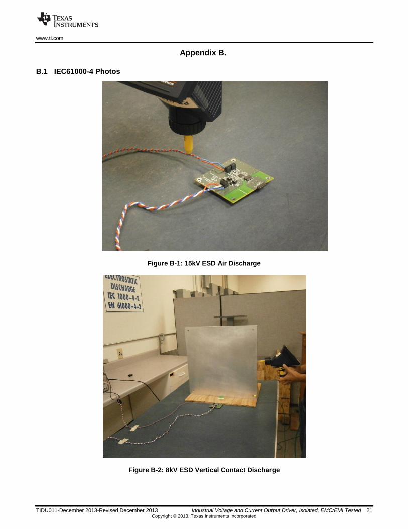
See Appendix B for photos of conventional test setups for each of the tests mentioned in this section. Full details of each of the IEC61000-4 tests are licensed by the IEC and must be purchased.
2.3.1 IEC61000-4-2
IEC61000-4-2 is the electrostatic discharge (ESD) immunity test. This test simulates the electrostatic discharge of an operator directly onto an electrical component. To simulate this event, an ESD generator applies ESD pulses to the EUT either through air discharge or through vertical and horizontal coupling planes. Air discharge tests are conducted near any exposed I/O terminal.
I OU
T/I
OU
T-P
EA
K
Time - ns
0 10 20 30 40 50 60 70 80
0.2
0.4
0.6
0.8
1.0
Figure 3: IEC61000-4 ESD Test Pulse

www.ti.com
TIDU011-December 2013-Revised December 2013 Industrial Voltage and Current Output Driver, Isolated, EMC/EMI Tested 5 Copyright © 2013, Texas Instruments Incorporated
The ESD test pulse is pictured in Figure 3. The ESD test pulse is a high frequency transient with a pulse period of less than 100ns. The pulse is a high-voltage signal, ranging from 4 kV to 15 kV depending on the threat level appropriate for the EUT. The complete ESD test requires 10 sequential discharges of each positive and negative polarity for each test configuration.
2.3.2 IEC61000-4-3
IEC61000-4-3 is the radiated immunity (RI) test. This test simulates exposure to high frequency radiated emissions, such as radio devices or other emissions common in industrial processes. The frequency range and field strength of the radiated signals vary in this test based on the type of EUT. For this design the tested frequency range was 80 MHz – 1 GHz and the field strength was 20 V/m.
2.3.3 IEC61000-4-4
IEC61000-4-4 is the burst immunity, or electrically fast transient (EFT) test. This test simulates day to day switching transients from various sources in a typical industrial application space. The test is performed on power, signal, and earth wires – or a subset depending on what is appropriate for the EUT.
VO
UT/V
OU
T-P
EA
K
Time - ns
0 10 20 30 40 50 60 70 80
0.2
0.4
0.6
0.8
1.0
200µs
400µs
300µs
15µs
1 2 3
10s 10s
t
t
t
V
V
V
Figure 4: IEC61000-4 EFT Test Pulses
In this test a burst generator produces a series of EFT bursts, each lasting 15ms with 300ms in between bursts. The pulse rate of each burst is approximately 5 kHz. A typical test will expose the EUT to 1 – 3 minutes of EFT bursts. Similar to the ESD test pulse, the EFT pulses are a high frequency signal but the magnitude of the EFT test pulse only ranges from 0.25 kV to 4 kV. Bursts of both positive and negative polarity are applied.
2.3.4 IEC61000-4-6
IEC61000-4-6 is the conducted immunity (CI) test. This test simulates exposure to radio frequency transmitters in the range of 15 kHz to 80 MHz. Like the RI test, the field strength of the CI transmitter can vary, ranging from 3 V/m to 10 V/m.
2.4 Protection Circuitry
The IEC61000-4 transients have two main components: a high frequency component and a high energy component. These two properties can be leveraged with a strategy of attenuation and diversion by the protection circuitry to deliver robust immunity.
Attenuation uses passive components, primarily resistors and capacitors to attenuate high-frequency transients and to limit series current. Ferrite beads can also be used and are useful to maintain dc accuracy while still delivering the ability to limit current from high frequency transients. This circuit utilizes capacitors placed at each of the voltage and current output terminals. A resistor is placed on the current output to limit current flowing into the IOUT terminal of the DAC8760 during exposure to high voltage transients. The voltage output stage uses a similar strategy with two resistors in the voltage output feedback loop in addition to a ferrite bead outside of the loop.
www.ti.com
6 Industrial Voltage and Current Output Driver, Isolated, EMC/EMI Tested TIDU011-December 2013-Revised December 2013 Copyright © 2013, Texas Instruments Incorporated
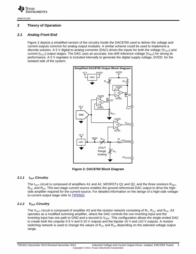
Diversion capitalizes on the high voltage properties of the transient signals by using diodes to clamp the transient within supply voltages or to divert the energy to ground. Transient voltage suppressor (TVS) diodes are helpful to protect against the IEC transients because they break down very quickly and often feature high power ratings which are critical to survive multiple transient strikes. Schottky diodes feature very low forward voltage drop and are used to clamp the voltage on the I/O lines to within the absolute maximum ratings of the DAC8760.
3 Component Selection
A detailed schematic for the design with all component values is shown in Figure 5.
Figure 5: Complete Schematic for DAC8760 with EMC/EMI Protection
3.1 DAC
DAC8760 was chosen for this design for its high level of integration which is helpful to simplify the design of an EMC/EMI protection solution.
The DAC8760 includes the DAC, amplifiers A1, A2, and A3, VREG, VREF, and all of the switches, transistors, and resistors required to create a configurable integrated solution for industrial voltage and current output drivers. The DAC8760 features a max 0.1% full-scale range (FSR) total-unadjusted-error (TUE) specification, which includes offset error, gain error, and integral non-linearity (INL) errors at 25°C. The 0.1% FSR TUE is valid for all of the voltage and current output stages providing a baseline for the final system accuracy. The max differential non-linearity (DNL) specification of +/-1 least significant bit (LSB) provides fully monotonic operation for both VOUT and IOUT.
The integral non-linearity (INL) specifications of 0.022% FSR for VOUT and 0.024% FSR for IOUT demonstrate high linearity and accuracy. The integrated VREF circuit provides a low temperature drift reference for the DAC, specified at 10 ppm/°C. The 4-wire SPI communication bus features a daisy-chain option that allows multiple DAC8760 devices to be controlled through a single 4-channel digital isolator, enabling a group-isolated multiple output system.
3.2 TVS Diode
A bidirectional TVS diode can be used to divert high voltage transients to ground for systems that utilize symmetrical supply voltages, such as ±15 V. For non-symmetrical supply voltages two unidirectional TVS diodes must be used. In both cases, diode selection is based on working voltage, breakdown voltage, and power rating.
Isolation
Barrier
Field
Connections
DVDD DVDD-EN AVDD
LATCH
SCLK
SDIN
SDO
GNDHART IN
DAC8760
AVSS
REFINREFOUT
+VSENSE
VOUT
-VSENSE
CMP
IOUTGND
VDD
SCLK
MOSI
MISO
/CS
Digital Controller
ISO7641
OUTA
OUTB
OUTC
GND2
VCC2
INA
INB
INC
GND1
VCC1
OUTD IND
+15V
-15V
100nF
15Ω Current Output0-20mA, 4-20mA, 0-24mA
0-5V, 0-10V, ±5V, ±10V Voltage Output
+15V
-15V
Ferrite Bead15Ω
15Ω
1nF
0.1mF22nF
+15V-15V
0.1mF
100pF
0.1mF
100pF
0.1mF
0.1mF0.1mF
0.1mF
15V
Bidirectional
TVS
15V
Bidirectional
TVS
100nF
www.ti.com
TIDU011-December 2013-Revised December 2013 Industrial Voltage and Current Output Driver, Isolated, EMC/EMI Tested 7 Copyright © 2013, Texas Instruments Incorporated
The working voltage specification of a diode defines the largest reverse voltage that the diode is meant to be operated at continuously without it conducting. This is the voltage at the “knee” of the reverse breakdown curve where the diode begins to break down and exhibits some small leakage current. As the voltage increases above the working voltage, more current will begin to flow through the diode. The breakdown voltage defines the reverse voltage at which the diode is fully allowing current to flow. It is important to keep in mind that if excessive current flows through a diode, the breakdown voltage will rise.
The diode breakdown voltage should be low enough to protect all components connected to the output terminals and to provide headroom for the breakdown voltage to rise with reasonably large currents. The DAC8760 absolute maximum supply ratings are specified as 40V between AVDD and AVSS, 40V for AVDD to ground, and -20V for AVSS to ground. To match the power-supply voltages, a bidirectional TVS diode with a working voltage of 15 V, a breakdown voltage of 16.7 V, and power rating of 400 W was chosen.
An additional parameter to consider for TVS diode selection is leakage current. At the working voltage, when the diode is not operating in its breakdown region, some current will flow through the diode and can affect system accuracy. The diode selected for this design features 1 µA maximum leakage current at the working voltage.
3.3 Schottky Diode
All Schottky diodes feature low forward voltage drop for reasonable currents but the forward voltage drop may increase beyond being useful in the circuit when exposed to excessive current. The Schottky diode used in this design must maintain low enough forward voltage drop to keep the voltage at the input terminals within the absolute maximum ratings for all components connected to the output terminals. The diode used in this design features forward voltage drop of 1.5 V when 1 A is flowing through the diode, which means the diodes will clamp at 16.5 V for transients with 1 A of current.
Like the TVS diodes, Schottky diodes can contribute some leakage current on the voltage and current outputs based on the reverse leakage current specification. Reverse leakage current is usually specified at a specific reverse voltage. The diode used in this design has a reverse leakage current specification of 1 µA at 70V reverse voltage.
3.4 Passive Components
The capacitors placed on the output terminals of the voltage and current outputs are used in combination with the transient generator’s source impedance to attenuate and slow down signals before they are clamped by the TVS diodes or Schottky diodes. The size of the capacitor plays an important role for delivering class A performance in the IEC61000-4 tests at the cost of system bandwidth.
For the current output a resistor is placed between the TVS diodes and Schottky diodes to provide a pass element between the TVS clamp voltage and the Schottky as well as to limit current flowing into the DAC8760 output terminals. This resistor should be sized appropriately to provide some series current limit without causing compliance voltage at the current output.
The voltage output uses a ferrite bead between the TVS diodes and Schottky diodes for the same purpose as the resistor on the current output. Since the component location is not included in the voltage output feedback loop, a ferrite bead was used instead of a resistor to maintain dc accuracy. The selected ferrite has a dc impedance of 40 mΩ and an impedance of 500 Ω at 100 MHz. Two additional resistors are included in the voltage output feedback loop to provide additional current limiting to the DAC8760 output terminals.
3.5 Digital Isolator
The four serial data signals required to communicate bi-directionally with the DAC8760 are SCLK, DIN, SDO, and LATCH. In order to maintain isolation from the host controller, these signals must be isolated through a digital isolator. The ISO7641 is a 25 MBPS digital isolator that features >4 kV galvanic isolation.
www.ti.com
8 Industrial Voltage and Current Output Driver, Isolated, EMC/EMI Tested TIDU011-December 2013-Revised December 2013 Copyright © 2013, Texas Instruments Incorporated
4 Calculation
During normal operation of the DAC8760, when no transient signals are applied to the output terminals, it is important that the protection elements do not contribute substantial error to the system. This section explores the impact of the protection circuitry on the voltage and current outputs of the DAC8760.
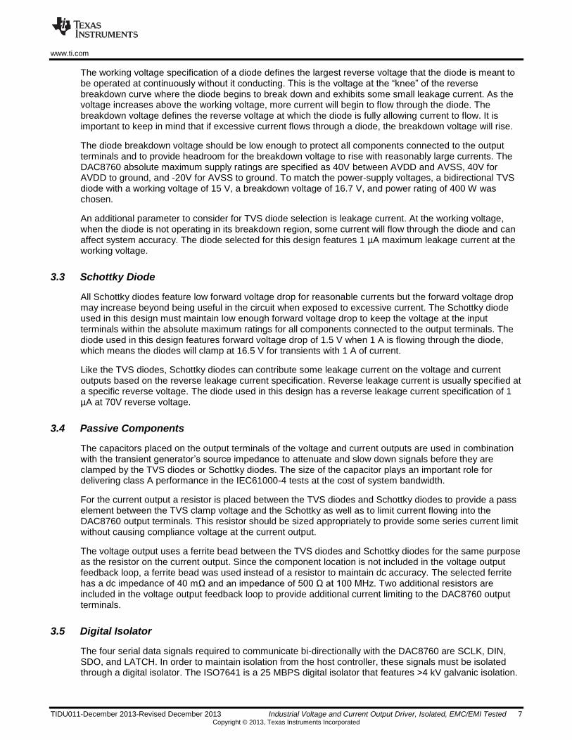
4.1 IOUT Accuracy
The resistors and capacitors used in the protection circuit have no impact on the dc accuracy of the current output.
A typical TVS diode provides a maximum leakage current specification, specified at the working voltage. The diode used in this design has a working voltage of 15 V and 1 µA of leakage at this voltage, but the voltage at the current output should never approach 15 V during normal operation since it will approach its compliance voltage first, which is 13V for a DAC8760 with ±15 V analog supplies and no load. Equation 1 can be used to calculate compliance voltage for the DAC8760.
V2AVDDVCompliance ( 1 )
Schottky diode leakage is also provided under a specific set of conditions. For a Schottky diode reverse leakage current is specified at a specific reverse voltage. The diodes used in this design will have 1 µA of leakage current at 70 V reverse voltage. However, the diodes will only have 15 V of reverse voltage as used in this design.
Since both the TVS diodes and the Schottky diodes stay away from operating corners that would create substantial error for the system current output, the current output performance is defined by the
performance of the DAC8760, shown in
Figure 6 and Table 3.
Figure 6: DAC8760 DC IOUT Specifications
Table 3. Calculated IOUT Circuit Performance
Goals Calculated
Current (0-24 mA) Offset (%FSR) N/A +/-0.01
Gain Error (%FSR) N/A +/-0.01
INL (%FSR) N/A +/-0.024
www.ti.com
TIDU011-December 2013-Revised December 2013 Industrial Voltage and Current Output Driver, Isolated, EMC/EMI Tested 9 Copyright © 2013, Texas Instruments Incorporated
TUE (%FSR) 0.1% +/-0.08
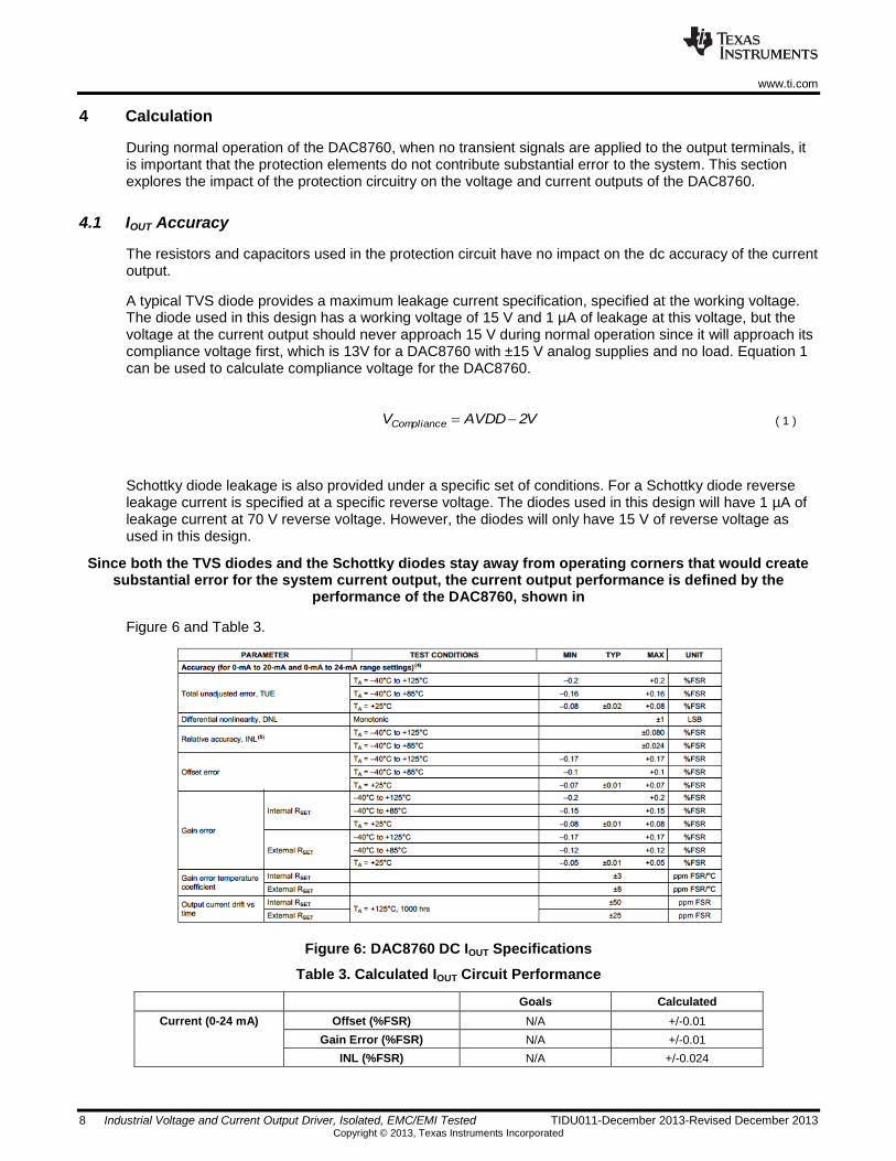
4.2 VOUT Accuracy
Leakage currents of the diodes used in the protection scheme will have negligible effect, less than 1 mV, on the voltage output of the DAC8760 as the internal amplifiers will easily compensate for the small change in source or sink current. This is shown by the voltage output load regulation curve from the DAC8760 datasheet in Figure 7.
Figure 7: DAC8760 VOUT Load Regulation
The series pass element used for the voltage output stage is a ferrite bead whose maximum impedance at dc is specified as 40 mΩ. If the DAC8760 was sourcing nearly its maximum current, this would only create an offset error of 1 mV – typical operation will avoid this region.
The protection circuit contributes negligible error to the system voltage output, therefore the voltage output performance is defined by the performance of the DAC8760, shown in Figure 8 and Table 4.
Figure 8: DAC8760 VOUT Specifications
Table 4. Calculated VOUT Circuit Performance
Goals Calculated
Voltage (±10 V) Offset (mV) N/A +/-1
Gain Error (%FSR) N/A +/-0.01
INL (%FSR) N/A +/-0.022
TUE (%FSR) 0.1% +/-0.03

www.ti.com
10 Industrial Voltage and Current Output Driver, Isolated, EMC/EMI Tested TIDU011-December 2013-Revised December 2013 Copyright © 2013, Texas Instruments Incorporated
5 PCB Design
The PCB schematic and bill of materials can be found in Appendix A.20
5.1 PCB Layout
For optimal performance of this design follow standard PCB layout guidelines, including proper decoupling close to all integrated circuits and adequate power and ground connections with large copper pours.
Additional considerations must be made for providing robust EMC/EMI immunity. All protection elements should be placed as close to the output connectors as possible to provide a controlled return path for transient currents that does not cross sensitive components. To allow optimum current flow wide, low-impedance, low-inductance traces should be used along the output signal path and protection elements. When possible copper pours are used in place of traces. Stitching the pours provides an effective return path around the PCB and helps reduce the impact of radiated emissions
Figure 9: Altium PCB Layout

www.ti.com
TIDU011-December 2013-Revised December 2013 Industrial Voltage and Current Output Driver, Isolated, EMC/EMI Tested 11 Copyright © 2013, Texas Instruments Incorporated
6 Verification & Measured Performance
6.1 0-24 mA Current Output
DC transfer function data for the IOUT circuit in 0-24 mA mode was collected using an 8.5 digit multi-meter to measure the output of the circuit while driving a 300 Ω load. The measurement results are shown in Table 5 and Figure 10Error! Reference source not found..
Table 5. Measured IOUT Circuit Performance
Goals Calculated Measured
Current (0-24 mA) Offset (%FSR) N/A +/-0.01 0.007
Gain Error (%FSR) N/A +/-0.01 0.034
INL (%FSR) N/A +/-0.024 0.007
TUE (%FSR) 0.1% +/-0.08 0.042
Figure 10. IOUT Circuit 0-24 mA Output Transfer Function
0
4
8
12
16
20
24
0 10000 20000 30000 40000 50000 60000
Outp
ut C
urr
ent (m
A)
Input Code
0-24 mA
C003
Warning! Do not move, alter, violate, or delete red bounding box or this warning!
Warning! Do not move, alter, violate, or delete red bounding box or this warning!
65535

www.ti.com
12 Industrial Voltage and Current Output Driver, Isolated, EMC/EMI Tested TIDU011-December 2013-Revised December 2013 Copyright © 2013, Texas Instruments Incorporated
6.2 VOUT Circuit
DC transfer function data for the VOUT circuit in +/-10V mode was collected using an 8.5 digit multi-meter to measure the output of the circuit while driving a 1 kΩ load. The measurement results are shown in Table 6 and Figure 11.
Table 6. Measured VOUT Circuit Performance
Goals Calculated Measured
Voltage (+/-10 V) Offset (mV) N/A +/-1 0.54
Gain Error (%FSR) N/A +/-0.01 0.022
INL (%FSR) N/A +/-0.022 0.007
TUE (%FSR) 0.1% +/-0.03 0.014
Figure 11. VOUT +/-10 V Output Transfer Function
-10
-8
-6
-4
-2
0
2
4
6
8
10
0 10000 20000 30000 40000 50000 60000
Outp
ut V
oltage (
V)
Input Code
+/-10 V
C003
Warning! Do not move, alter, violate, or delete red bounding box or this warning!
Warning! Do not move, alter, violate, or delete red bounding box or this warning!
65535
www.ti.com
TIDU011-December 2013-Revised December 2013 Industrial Voltage and Current Output Driver, Isolated, EMC/EMI Tested 13 Copyright © 2013, Texas Instruments Incorporated
7 Certification Testing Results
The IEC61000-4 certifications clearly define conditions for class B, C, and D performance but do not provide an explicit definition for class A. Class A conditions are defined by the manufacturer. For this EUT class A performance will be assigned for outputs that stay within 0.1% FSR of their intended value, corrected for dc errors intrinsic to the DAC, during exposure to each disturbance. The DAC8760 is set to the 0-24 mA range for current outputs and the ±10 V range for voltage outputs.
The IEC61000-4 certifications do not specify what supporting equipment is used to monitor the output of the EUT. For this design, an Agilent 34401A 6 ½ digit digital multi-meter with its resolution set to fast 5 ½ digit mode was selected to monitor the output.
Raw waveforms of each output during exposure to the IEC61000-4 tests are available in the design archive associated with this document.
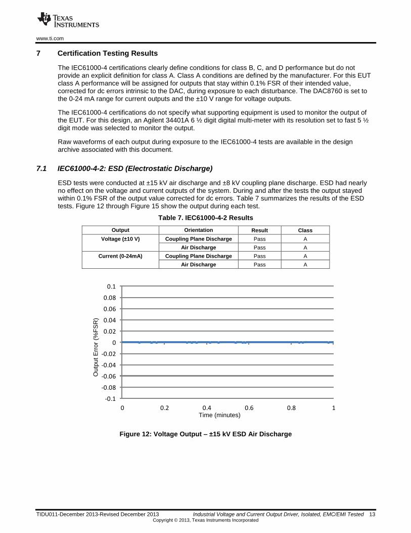
7.1 IEC61000-4-2: ESD (Electrostatic Discharge)
ESD tests were conducted at ±15 kV air discharge and ±8 kV coupling plane discharge. ESD had nearly no effect on the voltage and current outputs of the system. During and after the tests the output stayed within 0.1% FSR of the output value corrected for dc errors. Table 7 summarizes the results of the ESD tests. Figure 12 through Figure 15 show the output during each test.
Table 7. IEC61000-4-2 Results
Output Orientation Result Class
Voltage (±10 V) Coupling Plane Discharge Pass A
Air Discharge Pass A
Current (0-24mA) Coupling Plane Discharge Pass A
Air Discharge Pass A
-0.1
-0.08
-0.06
-0.04
-0.02
0
0.02
0.04
0.06
0.08
0.1
0 0.2 0.4 0.6 0.8 1Time (minutes)
Ou
tpu
t E
rro
r (%
FS
R)
Figure 12: Voltage Output – ±15 kV ESD Air Discharge

www.ti.com
14 Industrial Voltage and Current Output Driver, Isolated, EMC/EMI Tested TIDU011-December 2013-Revised December 2013 Copyright © 2013, Texas Instruments Incorporated
-0.1
-0.08
-0.06
-0.04
-0.02
0
0.02
0.04
0.06
0.08
0.1
0 0.2 0.4 0.6 0.8 1Time (minutes)
Ou
tpu
t E
rro
r (%
FS
R)
Figure 13: Voltage Output – ±8 kV ESD Vertical and Horizontal Coupling Plane Discharge
-0.1
-0.08
-0.06
-0.04
-0.02
0
0.02
0.04
0.06
0.08
0.1
0 0.1 0.2 0.3 0.4 0.5 0.6 0.7Time (minutes)
Ou
tpu
t E
rro
r (%
FS
R)
Figure 14: Current Output – ±15 kV ESD Air Discharge

www.ti.com
TIDU011-December 2013-Revised December 2013 Industrial Voltage and Current Output Driver, Isolated, EMC/EMI Tested 15 Copyright © 2013, Texas Instruments Incorporated
-0.1
-0.08
-0.06
-0.04
-0.02
0
0.02
0.04
0.06
0.08
0.1
0 0.1 0.2 0.3 0.4 0.5 0.6 0.7Time (minutes)
Ou
tpu
t E
rro
r (%
FS
R)
Figure 15: Current Output – ±8 kV ESD Vertical and Horizontal Coupling Plane Discharge
7.2 IEC61000-4-3: RI (Radiated Immunity)
Exposure to radiated emissions with field strength of 20 V/m caused the current output to deviate slightly and caused almost no deviations on the voltage output. The current output remained within 0.1% FSR of the output value corrected for dc errors. After the test was completed both the voltage and current outputs returned to normal operation without deviation. Table 8 summarizes the results of each test. Figure 16 and Figure 17 show the outputs during each test.
Table 8. IEC61000-4-3 Results
Output Orientation Result Class
Voltage (±10 V) Vertical Pass A
Horizontal Pass A
Current (0-24mA) Vertical Pass A
Horizontal Pass A

www.ti.com
16 Industrial Voltage and Current Output Driver, Isolated, EMC/EMI Tested TIDU011-December 2013-Revised December 2013 Copyright © 2013, Texas Instruments Incorporated
-0.1
-0.08
-0.06
-0.04
-0.02
0
0.02
0.04
0.06
0.08
0.1
0 5 10 15 20 25
Horizontal
Vertical
Time (minutes)
Ou
tpu
t E
rro
r (%
FS
R)
Figure 16: Voltage Output – 20 V/m Radiated Immunity
-0.1
-0.08
-0.06
-0.04
-0.02
0
0.02
0.04
0.06
0.08
0.1
0 5 10 15 20 25
Horizontal
Vertical
Time (minutes)
Ou
tpu
t E
rro
r (%
FS
R)
Figure 17: Current Output – 20 V/m Radiated Immunity
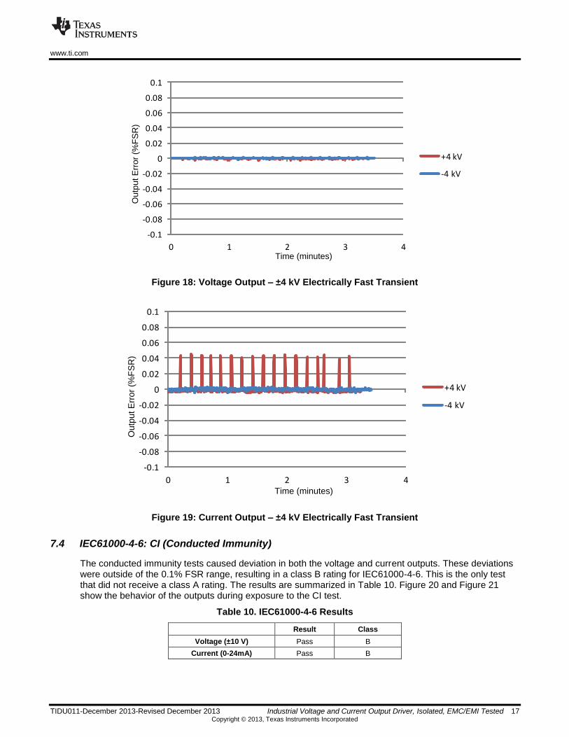
7.3 IEC61000-4-4: EFT (Electrically Fast Transient)
The electrical fast transient bursts had almost no effect on the voltage output. The current output was not disturbed by the negative polarity EFT bursts, but slight deviations were seen with positive polarity EFT bursts. After testing was complete normal functionality was restored. Table 9 summarizes the results of each test. Figure 20 and Figure 21 show the voltage and current outputs during each test.
Table 9. IEC61000-4-4 Results
Output Orientation Result Class
Voltage (±10 V) Vertical Pass A
Horizontal Pass A
Current (0-24mA) Vertical Pass A
Horizontal Pass A
www.ti.com
TIDU011-December 2013-Revised December 2013 Industrial Voltage and Current Output Driver, Isolated, EMC/EMI Tested 17 Copyright © 2013, Texas Instruments Incorporated
-0.1
-0.08
-0.06
-0.04
-0.02
0
0.02
0.04
0.06
0.08
0.1
0 1 2 3 4
+4 kV
-4 kV
Time (minutes)
Ou
tpu
t E
rro
r (%
FS
R)
Figure 18: Voltage Output – ±4 kV Electrically Fast Transient
-0.1
-0.08
-0.06
-0.04
-0.02
0
0.02
0.04
0.06
0.08
0.1
0 1 2 3 4
+4 kV
-4 kV
Time (minutes)
Ou
tpu
t E
rro
r (%
FS
R)
Figure 19: Current Output – ±4 kV Electrically Fast Transient
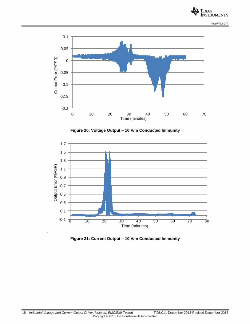
7.4 IEC61000-4-6: CI (Conducted Immunity)
The conducted immunity tests caused deviation in both the voltage and current outputs. These deviations were outside of the 0.1% FSR range, resulting in a class B rating for IEC61000-4-6. This is the only test that did not receive a class A rating. The results are summarized in Table 10. Figure 20 and Figure 21 show the behavior of the outputs during exposure to the CI test.
Table 10. IEC61000-4-6 Results
Result Class
Voltage (±10 V) Pass B
Current (0-24mA) Pass B
www.ti.com
18 Industrial Voltage and Current Output Driver, Isolated, EMC/EMI Tested TIDU011-December 2013-Revised December 2013 Copyright © 2013, Texas Instruments Incorporated
-0.2
-0.15
-0.1
-0.05
0
0.05
0.1
0 10 20 30 40 50 60 70Time (minutes)
Ou
tpu
t E
rro
r (%
FS
R)
Figure 20: Voltage Output – 10 V/m Conducted Immunity
.
-0.1
0.1
0.3
0.5
0.7
0.9
1.1
1.3
1.5
1.7
0 10 20 30 40 50 60 70 80Time (minutes)
Ou
tpu
t E
rro
r (%
FS
R)
Figure 21: Current Output – 10 V/m Conducted Immunity

www.ti.com
TIDU011-December 2013-Revised December 2013 Industrial Voltage and Current Output Driver, Isolated, EMC/EMI Tested 19 Copyright © 2013, Texas Instruments Incorporated
8 Modifications
The DAC7760 is the 12-bit equivalent to the DAC8760 and can be directly substituted for applications where 16-bit resolution is not required. Designs that only require a current output can replace the DAC8760 with the DAC8750 (16-bit) or DAC7750 (12-bit) with minimal changes.
The circuitry inside of the DAC8760 family of products can be replicated with several discrete DACs, op-amps, transistors, and passive components. Alternatively, the XTR family of products from Texas Instruments, such as the XTR300, provide the complete analog front-end for 4-20 mA applications and can simply be paired with a DA to deliver a complete system.
The output protection circuit described in this design is specifically tailored to the DAC8760 and associated family of devices with bipolar 15 V supplies. Modifying the power supply voltages used in this design may require the selection of different components, such as higher or lower breakdown voltage TVS diodes. Discrete solutions that use multiple integrated circuits may also need to choose different protection components for appropriate protection.
Furthermore, the protection circuit in this design is only intended to be applied to IEC61000-4-2, IEC61000-4-3, IEC61000-4-4, and IEC61000-4-6. Other immunity tests, like surge immunity (IEC61000-4-5), are not considered for this design and may require additional components such as transient blocking units or fusing elements to handle the power levels associated with them.
9 About the Authors
Kevin Duke is an applications engineer in the precision digital to analog converters group at Texas Instruments where he supports industrial and catalog products and applications. Kevin received his BSEE from Texas Tech University in 2010.
Collin Wells is an applications engineer in the Precision Linear group at Texas Instruments where he supports industrial products and applications. Collin received his BSEE from the University of Texas, Dallas.
10 Acknowledgements & References
The authors wish to acknowledge NTS (National Technical Systems) in Plano, TX for their assistance performing the electromagnetic compatibility tests.
1. IEC Publication 61000-4-2 “Electromagnetic Compatibility (EMC) – Part 4-2: Testing and Measurement Techniques – Electrostatic Discharge Immunity Test,” International Electrotechnical Commission, 2008.
2. IEC Publication 61000-4-3 “Electromagnetic Compatibility (EMC) – Part 4-3: Testing and Measurement Techniques – Radiated, Radio-Frequency, Electromagnetic Field Immunity Test,” International Electrotechnical Commission, 2006.
3. IEC Publication 61000-4-4 “Electromagnetic Compatibility (EMC) – Part 4-4: Testing and Measurement Techniques – Electrical Fast Transient/Burst Immunity Test,” International Electrotechnical Commission, 2012.
4. IEC Publication 61000-4-6 “Electromagnetic Compatibility (EMC) – Part 4-6: Testing and Measurement Techniques – Immunity to Conducted Disturbances, Induced by Radio-Frequency Fields,” International Electrotechnical Commission, 2008.
5. H. Ott, Electromagnetic Compatibility. John Wiley & Sons Inc., 2009.

www.ti.com
20 Industrial Voltage and Current Output Driver, Isolated, EMC/EMI Tested TIDU011-December 2013-Revised December 2013 Copyright © 2013, Texas Instruments Incorporated
Appendix A.
A.1 Electrical Schematic
Figure A-1: Electrical Schematic
A.2 Bill of Materials
Figure A-2: Bill of Materials
www.ti.com
TIDU011-December 2013-Revised December 2013 Industrial Voltage and Current Output Driver, Isolated, EMC/EMI Tested 21 Copyright © 2013, Texas Instruments Incorporated
Appendix B.
B.1 IEC61000-4 Photos
Figure B-1: 15kV ESD Air Discharge
Figure B-2: 8kV ESD Vertical Contact Discharge

www.ti.com
22 Industrial Voltage and Current Output Driver, Isolated, EMC/EMI Tested TIDU011-December 2013-Revised December 2013 Copyright © 2013, Texas Instruments Incorporated
Figure B-3: 8kV ESD Horizontal Contact Discharge
Figure B-4: EFT Test Setup

www.ti.com
TIDU011-December 2013-Revised December 2013 Industrial Voltage and Current Output Driver, Isolated, EMC/EMI Tested 23 Copyright © 2013, Texas Instruments Incorporated
Figure B-5: Horizontal Radiated Immunity
Figure B-5: Vertical Radiated Immunity
IMPORTANT NOTICE FOR TI REFERENCE DESIGNSTexas Instruments Incorporated ("TI") reference designs are solely intended to assist designers (“Buyers”) who are developing systems thatincorporate TI semiconductor products (also referred to herein as “components”). Buyer understands and agrees that Buyer remainsresponsible for using its independent analysis, evaluation and judgment in designing Buyer’s systems and products.TI reference designs have been created using standard laboratory conditions and engineering practices. TI has not conducted anytesting other than that specifically described in the published documentation for a particular reference design. TI may makecorrections, enhancements, improvements and other changes to its reference designs.Buyers are authorized to use TI reference designs with the TI component(s) identified in each particular reference design and to modify thereference design in the development of their end products. HOWEVER, NO OTHER LICENSE, EXPRESS OR IMPLIED, BY ESTOPPELOR OTHERWISE TO ANY OTHER TI INTELLECTUAL PROPERTY RIGHT, AND NO LICENSE TO ANY THIRD PARTY TECHNOLOGYOR INTELLECTUAL PROPERTY RIGHT, IS GRANTED HEREIN, including but not limited to any patent right, copyright, mask work right,or other intellectual property right relating to any combination, machine, or process in which TI components or services are used.Information published by TI regarding third-party products or services does not constitute a license to use such products or services, or awarranty or endorsement thereof. Use of such information may require a license from a third party under the patents or other intellectualproperty of the third party, or a license from TI under the patents or other intellectual property of TI.TI REFERENCE DESIGNS ARE PROVIDED "AS IS". TI MAKES NO WARRANTIES OR REPRESENTATIONS WITH REGARD TO THEREFERENCE DESIGNS OR USE OF THE REFERENCE DESIGNS, EXPRESS, IMPLIED OR STATUTORY, INCLUDING ACCURACY ORCOMPLETENESS. TI DISCLAIMS ANY WARRANTY OF TITLE AND ANY IMPLIED WARRANTIES OF MERCHANTABILITY, FITNESSFOR A PARTICULAR PURPOSE, QUIET ENJOYMENT, QUIET POSSESSION, AND NON-INFRINGEMENT OF ANY THIRD PARTYINTELLECTUAL PROPERTY RIGHTS WITH REGARD TO TI REFERENCE DESIGNS OR USE THEREOF. TI SHALL NOT BE LIABLEFOR AND SHALL NOT DEFEND OR INDEMNIFY BUYERS AGAINST ANY THIRD PARTY INFRINGEMENT CLAIM THAT RELATES TOOR IS BASED ON A COMBINATION OF COMPONENTS PROVIDED IN A TI REFERENCE DESIGN. IN NO EVENT SHALL TI BELIABLE FOR ANY ACTUAL, SPECIAL, INCIDENTAL, CONSEQUENTIAL OR INDIRECT DAMAGES, HOWEVER CAUSED, ON ANYTHEORY OF LIABILITY AND WHETHER OR NOT TI HAS BEEN ADVISED OF THE POSSIBILITY OF SUCH DAMAGES, ARISING INANY WAY OUT OF TI REFERENCE DESIGNS OR BUYER’S USE OF TI REFERENCE DESIGNS.TI reserves the right to make corrections, enhancements, improvements and other changes to its semiconductor products and services perJESD46, latest issue, and to discontinue any product or service per JESD48, latest issue. Buyers should obtain the latest relevantinformation before placing orders and should verify that such information is current and complete. All semiconductor products are soldsubject to TI’s terms and conditions of sale supplied at the time of order acknowledgment.TI warrants performance of its components to the specifications applicable at the time of sale, in accordance with the warranty in TI’s termsand conditions of sale of semiconductor products. Testing and other quality control techniques for TI components are used to the extent TIdeems necessary to support this warranty. Except where mandated by applicable law, testing of all parameters of each component is notnecessarily performed.TI assumes no liability for applications assistance or the design of Buyers’ products. Buyers are responsible for their products andapplications using TI components. To minimize the risks associated with Buyers’ products and applications, Buyers should provideadequate design and operating safeguards.Reproduction of significant portions of TI information in TI data books, data sheets or reference designs is permissible only if reproduction iswithout alteration and is accompanied by all associated warranties, conditions, limitations, and notices. TI is not responsible or liable forsuch altered documentation. Information of third parties may be subject to additional restrictions.Buyer acknowledges and agrees that it is solely responsible for compliance with all legal, regulatory and safety-related requirementsconcerning its products, and any use of TI components in its applications, notwithstanding any applications-related information or supportthat may be provided by TI. Buyer represents and agrees that it has all the necessary expertise to create and implement safeguards thatanticipate dangerous failures, monitor failures and their consequences, lessen the likelihood of dangerous failures and take appropriateremedial actions. Buyer will fully indemnify TI and its representatives against any damages arising out of the use of any TI components inBuyer’s safety-critical applications.In some cases, TI components may be promoted specifically to facilitate safety-related applications. With such components, TI’s goal is tohelp enable customers to design and create their own end-product solutions that meet applicable functional safety standards andrequirements. Nonetheless, such components are subject to these terms.No TI components are authorized for use in FDA Class III (or similar life-critical medical equipment) unless authorized officers of the partieshave executed an agreement specifically governing such use.Only those TI components that TI has specifically designated as military grade or “enhanced plastic” are designed and intended for use inmilitary/aerospace applications or environments. Buyer acknowledges and agrees that any military or aerospace use of TI components thathave not been so designated is solely at Buyer's risk, and Buyer is solely responsible for compliance with all legal and regulatoryrequirements in connection with such use.TI has specifically designated certain components as meeting ISO/TS16949 requirements, mainly for automotive use. In any case of use ofnon-designated products, TI will not be responsible for any failure to meet ISO/TS16949.
Mailing Address: Texas Instruments, Post Office Box 655303, Dallas, Texas 75265Copyright © 2014, Texas Instruments Incorporated