
Printing control in any industrial sector - Screen printing Machine
Upload
steve-duccilliCategory
view
224download
0description
MAY
/JUN
E 20
11w
ww
.indu
stria
l-pr
intin
g.ne
t
Membrane Switches and Touchscreens
Specialty SubstratesRoll-to-Roll Printing
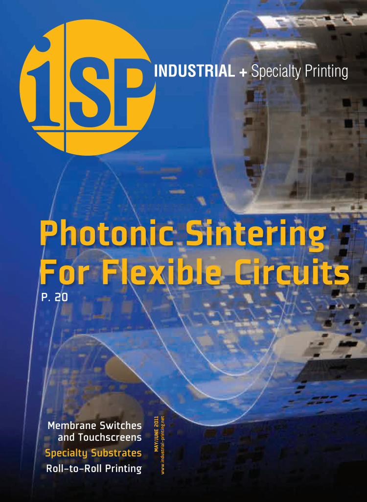
Photonic Sintering For Flexible CircuitsP. 20

Get the free mobile app athttp:/ /gettag.mobi
When you need fine line conductive traces, or the highest quality graphics to be printed with the utmost precision and consistency, MacDermid Autotype is in the forefront of developing screen printing stencil materials, substrates and scientifically proven software tools to achieve your ultimate goals. Improve consistency of your printed images with our unique capillary films, Capillex CP or CX and validate your prints using the "Acuity Index" from our QA software.
Specialty substrates are manufactured and converted in clean room environments to the most exacting standards to meet your highest quality needs for precision printing. Gain control of your web process by using Autostat heat stabilized polyesters for critical flexible circuitry. Hard coated, specialty finish film coatings are provided on polycarbonate and polyester for film insert molding, membrane touch switches, displays and touch screens.
For more information on our capabilities to support your printed electronic needs , visit: www.macdermidautotype.com or callToll free: 800-323-0632
The Right Partnerfor your printed electronic needs
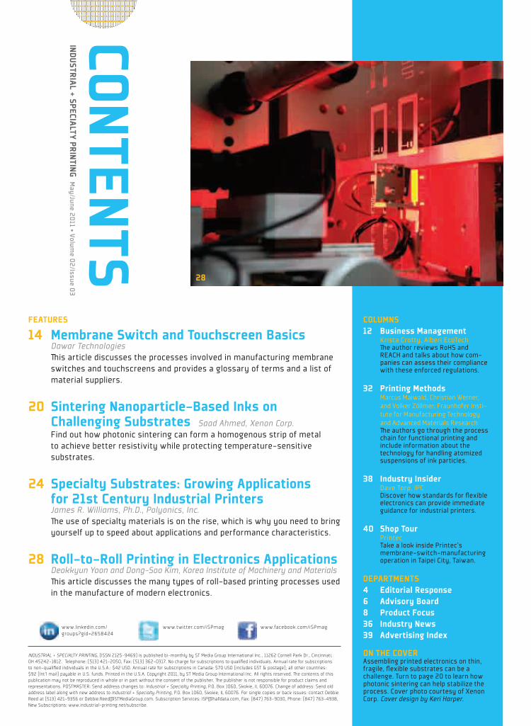
CONTENTSINDUSTRIAL + SPECIALTY PRINTING M
ay/June 2011 • Volume 02/Issue 03
28
FEATURES
14 Membrane Switch and Touchscreen BasicsDawar Technologies is article discusses the processes involved in manufacturing membrane switches and touchscreens and provides a glossary of terms and a list of material suppliers.
20 Sintering Nanoparticle-Based Inks on Challenging Substrates Saad Ahmed, Xenon Corp.Find out how photonic sintering can form a homogenous strip of metal to achieve better resistivity while protecting temperature-sensitive substrates.
24 Specialty Substrates: Growing Applications for 21st Century Industrial Printers James R. Williams, Ph.D., Polyonics, Inc. e use of specialty materials is on the rise, which is why you need to bring yourself up to speed about applications and performance characteristics.
28 Roll-to-Roll Printing in Electronics Applications Deokkyun Yoon and Dong-Soo Kim, Korea Institute of Machinery and Materials is article discusses the many types of roll-based printing processes used in the manufacture of modern electronics.
COLUMNS12 Business Management
Krista Crotty, Alberi EcoTech e author reviews RoHS and REACH and talks about how com-panies can assess their compliance with these enforced regulations.
32 Printing Methods Marcus Maiwald, Christian Werner, and Volker Zöllmer; Fraunhofer Insti-tute for Manufacturing Technology and Advanced Materials Research e authors go through the process chain for functional printing and include information about the technology for handling atomized suspensions of ink particles.
38 Industry InsiderDave Torp, IPCDiscover how standards for fl exible electronics can provide immediate guidance for industrial printers.
40 Shop TourPrintecTake a look inside Printec’s membrane-switch-manufacturing operation in Taipei City, Taiwan.
DEPARTMENTS4 Editorial Response6 Advisory Board8 Product Focus36 Industry News39 Advertising Index
ON THE COVERAssembling printed electronics on thin, fragile, fl exible substrates can be a challenge. Turn to page 20 to learn how photonic sintering can help stabilize the process. Cover photo courtesy of Xenon Corp. Cover design by Keri Harper.
www.linkedin.com/groups?gid=2658424
www.twitter.com/iSPmag www.facebook.com/iSPmag
INDUSTRIAL + SPECIALTY PRINTING, (ISSN 2125-9469) is published bi-monthly by ST Media Group International Inc., 11262 Cornell Park Dr., Cincinnati, OH 45242-1812. Telephone: (513) 421-2050, Fax: (513) 362-0317. No charge for subscriptions to qualifi ed individuals. Annual rate for subscriptions to non-qualifi ed individuals in the U.S.A.: $42 USD. Annual rate for subscriptions in Canada: $70 USD (includes GST & postage); all other countries: $92 (Int’l mail) payable in U.S. funds. Printed in the U.S.A. Copyright 2011, by ST Media Group International Inc. All rights reserved. e contents of this publication may not be reproduced in whole or in part without the consent of the publisher. e publisher is not responsible for product claims and representations. POSTMASTER: Send address changes to: Industrial + Specialty Printing, P.O. Box 1060, Skokie, IL 60076. Change of address: Send old address label along with new address to Industrial + Specialty Printing, P.O. Box 1060, Skokie, IL 60076. For single copies or back issues: contact Debbie Reed at (513) 421-9356 or [email protected]. Subscription Services: [email protected], Fax: (847) 763-9030, Phone: (847) 763-4938, New Subscriptions: www.industrial-printing.net/subscribe.
DOUTHITT
Contact us for more information on Douthitt’s complete line of Exposure Units, Vacuum Frames, CTS Imagers, Dryers, Inspection Tables, High Wattage UV Printing Lamps, Integrators and Blankets for any vacuum frame.
Visit us at www.douthittcorp.com
CONVENTIONAL OR CTS - DOUTHITT HAS THE OPTIMAL SOLUTION!
Contact us for a free catalog!
Complete Drying of Screens
The World’s Best Metal Halide Lamps
Olec Olite & Theimer Violux Lamps & Parts in Stock!
THE DOUTHITT CORPORATION
and solid ink technology enables imaging
image quality without compromising on throughput or consumable cost. Call us to see if CTS is right for you.
Douthitt’s self contained screen exposure systems provide the best vacuum contact and the best registration. Combined with our
sharpest resolution, guaranteed coverage, shorter exposures and completely hardened emulsion.
4 | INDUSTRIAL + SPECIALTY PRINTING www.industrial-printing.net
elastomeric and incompressible, the lm contracts in thickness and expands in area. The technology works like an elastomeric capacitor that is capable of changing ca-pacitance by applying a voltage or by an external mechanical force.
EPAM lm turns into an actuator by at-taching frames or materials that direct the motion to the desired axis. EPAM achieves motion (strain) from this electrostatic pres-sure as compared to other technologies. The displacement is a function of the area of EPAM, and the force exerted is a func-tion of the number of layers of EPAM. The electrode layer of the EPAM can be pat-terned to achieve speci c regions and di-rections of motions. The architecture along with con gurations were developed and patented by SRI Int’l and are now licensed exclusively to Arti cial Muscle, Inc.
In March 2010, Bayer MaterialScience LLC acquired Arti cial Muscle, Inc. Bayer recognized the need for tactile, or haptic, feedback in consumer electronic products that use touchscreens—products such as portable gaming controllers, industrial con-trols, and casino games. The rumble packs common to hand-held game controllers are only able to produce simple, one-dimen-sional effects from a single frequency. The time lag felt as the motor spins up or down disassociates the feel from the event. With Bayfol Re ex, a printed, customized actua-tor technology, it is said that the results are real-time effects with high- delity feel.
Let’s take it out of the game venue. Could a blind person be able to use an adapted smart phone when given touch responses? Could people who had speci c fears ( ying, falling, etc.) be able to face simulated situations through haptic re-sponses? What other applications can t? It will be interesting to see how many areas this will affect in the developing world of technology.
They say that when you lose one sense, the others take over. Recently I came down with the u, which ended up blocking my senses of smell, hearing, and taste. After a while, even my eyes didn’t see as clearly as they usually do. It wasn’t the best of times, but it taught me to isolate my activities to those that did work and make my brain ignore the other negative responses—like Spock in Star Trek, who was really great at turning off feelings.
What does this have to with the current issue of iSP? Consider the article about membrane switches and touchscreens from Dawar. When it comes to making touchscreens, even on a at glass, a button should look like a button, click like a but-ton, and feel like a button to give the user a sensory awareness that everything works properly. Touchscreens and intermediate user interfaces with immediate tactile feedback should improve the usability and appeal of consumer electronic devices.
By combining the sense of touch with sound and sight, the user of touchscreens gets a much more natural experience. Ar-ti cial Muscle Inc. (AMI) is one company that focuses on haptic (touch) applications through the manufacture of actuator and sensing components and application of a proprietary technology platform called Electroactive Polymer Arti cial Muscle (EPAM).
How does EPAM work? EPAM com-prises a thin layer of dielectric polymer lm between two conductive, compliant electrodes. When a voltage potential is ap-plied across the electrodes, the Maxwellian pressure of the positive charge attracting the negative charge causes the electrodes to attract each other, and since the lm is
Industrial + Specialty Printingwww.industrial-printing.net
STEVE DUCCILLI Group [email protected]
GREGORY SHARPLESS Associate [email protected]
GAIL FLOWER [email protected]
BEN P. ROSENFIELD Managing [email protected]
KERI HARPER Art [email protected]
LINDA VOLZ Production [email protected]
BUSINESS DEVELOPMENT MANAGERSLou Arneberg – MidwestLisa Zurick – East US, East Canada, EuropeBen Stauss – West US, West Canada, Asia
EDITORIAL ADVISORY BOARDJoe Fjelstad, Dolf Kahle, Bruce Kahn, Ph.D., Rita Mohanty, Ph.D., Randall Sherman, Mike Young, Wim Zoomer
JERRY SWORMSTEDTChairman of the Board
TEDD SWORMSTEDTPresident
JOHN TYMOSKIAssociate Director/Online
CUSTOMER SERVICEIndustral + Specialty Printing MagazineCustomer ServiceP.O. Box 1060Skokie, IL 60076
[email protected]: 847-763-9040
Flex ose Artifi cial Muscles
GAIL FLOWEREditor
EDITORIAL RESPONSE

Don’t compromise
image quality
for speeD
The EFI Rastek H652 UV printer delivers best-in-class image quality, speed and white ink capability.
The EFI™ Rastek™ H652 UV hybrid printer is the perfect choice for stunning four-color and grayscale image quality that meets stringent customer demands fast. Direct-to-rigid, roll-to-roll and white ink capability let you offer more applications to get more business and profits. Get it all with the EFI Rastek H562. Call 800-875-7117 or visit efi.com/GetItAll6.
IMAGE QUALITY oR SPEED? EFI RASTEk GIVES YoU BoTH.
©2011 EFI. All rights reserved.
EFI 970 Rastek Ad I&SP.indd 1 4/13/11 8:37:34 AM

| IndustrIal + specIalty prIntIng www.industrial-printing.net
Joseph Fjelstad ([email protected]) is a 34-year veteran of the electronics-interconnection industry and is an international authority, author, columnist, lecturer,
and innovator who holds more than 150 issued and pending US patents in the field. He is the founder and president of Verdant Electronics, a firm dedicated to environmentally friendly electronics assembly. He is co-founder and CEO of SiliconPipe, a specialist in high-
speed interconnection-architecture design, much of which is based on flexible-circuit technology. Prior to founding SiliconPipe, he worked with IC-package-technology developer Tessera Technologies, where he was appointed the company’s first fellow. Fjelstad and his innovations have received many industry awards and accolades.
Joe FJelstadVerdant electronics
adVIsory board
Dolf Kahle ([email protected]) is the CEO of Twinsburg, OH-based Visual Marking Systems, Inc., (VMS), a company that specializes in the OEM durable-
product-identification market and manufactures overlays, decals, and decorative trim for Fortune 1000 companies. Beyond the OEM market, VMS also produces fleet graphics, P-O-P products, and durable signage for the public-transportation market. VMS is an
ISO 9000- certified company that enjoys statewide recognition as a Lean Enterprise. Kahle is an active member of SGIA, SPIRE, and GPI. He served on the SGIA board for more than 10 years and was its chairman in 1999. He is currently the chairman of SPIRE. He holds a bachelor’s degree in mechanical engineering from the University of Michigan and an MBA from Arizona State University.
dolF KahleVisual Marking systems, Inc.
Bruce Kahn ([email protected]) is a consultant who specializes in the multidisciplinary fields of printable electronics, nanotechnology, RFID, and smart
packaging. Kahn holds a Ph.D. in chemistry from the University of Nebraska and is the author of more than 75 publications, including the recently published “Developments in Printable Organic Transistors,” “Printed and Thin Film Photovoltaics and Batteries,” and
“Displays and Lighting: OLED, e-paper, electroluminescent and beyond.” He is a frequent lecturer and author, and he regularly teaches workshops in the U.S. and abroad.
bruce Kahn, ph.d.printed electronics consulting
Rita Mohanty ([email protected]) is the director of advanced development at Speedline Technology and a certified Six Sigma Master Black Belt instructor. She
has more than 15 years of experience in industries and academics relating to engineering and electronic polymers, electronic packaging, and board assembly. She is a patent holder and has authored and edited books on electronics and numerous technical papers. Mohanty
is active in and holds various leadership positions with IMAPS, SMTA, IPC, iNEME, and SGIA. She received her Ph.D. in chemical engineering from the University of Rhode Island.
rIta Mohanty, ph.d.speedline technology
Mike Young ([email protected]) has spent 40 years as a specialist in high-definition graphic and industrial screen printing. He is an SGIA Fellow, a member of the Academy
of Screen Printing Technology, and a recipient of the prestigious Swormstedt Award for technical writing. He frequently writes for industry trade publications and speaks at international industry events. Young has published several technical books on advanced
screen-printing techniques and frequently conducts seminars for high-profile screen-printing companies worldwide. Young is a consultant with Imagetek Consulting Int’l.
MIKe youngImagetek consulting Int’l.
Wim Zoomer ([email protected]) is owner of Nijmegen, Netherlands-based Technical Language, a consulting and communication business that focuses
on flatbed and reel-to-reel rotary screen printing and other printing processes. He has written numerous articles for international screen-printing, art, and glass-processing magazines and is frequently called on to translate technical documents, manuals, books,
advertisements, and other materials in English, French, German, Spanish, and Dutch. He is also the author of the book, “Printing Flat Glass,” as well as several case studies that appear online. He holds a degree in chemical engineering. You can visit his Website at www.technicallanguage.eu.
wIM zooMertechnical language
Randall Sherman ([email protected]) is the president and CEO of New Venture Research, a technology market research firm. He holds a B.S. in
astrophysics, an M.S. in electrical engineering from the University of Colorado, and an M.B.A. from Edinburgh School of Business. Visit www.newventureresearch.com for more information.
randall sherMannew Venture research

S e m i c o n d u c to r
P h otovo lta i c
l e d
m e m S
P r i n t e d / F l e x i b l e e l e c t r o n i c S
e m e r g i n g m a r k e t S
t h e P r e m i e r i n t e r n at i o n a l e v e n t S F o r m i c r o – a n d n a n o – S c a l e m a n u Fa c t u r i n g
SEMIExpositions
U P C O M I N G E V E N T S
JulY 12-14Moscone Center
San Francisco, Californiawww.semiconwest.org
SePtember 7-9 taipei World trade center
Taipei, Taiwanwww.semicontaiwan.org
october 11-13messe dresden
Dresden, Germany www.semiconeuropa.org
For the complete schedule of 2011 SEMI Expositions, visit
www.semi.org/events
S e m i c o n W e S t 2 0 1 1
S e m i c o n t a i W a n 2 0 1 1
S e m i c o n e u r o P a 2 0 1 1
north America’s largest microelectronics manufacturing event
More than 100 hours of technical conferences, sessions, anpresentations covering the microelectronics supply chain from design/EDA to advanced packaging and test
new—techZonE exhibit pavilions covering high-brightnessLEDs, MEMs, printed/flexible electronics, design, manufacturing services, materials, and secondary equipment and services
at the innovation technol
semiconductor cluster in Europe
and technology
where plastic, organic and printed technology meets manufacturing
| IndustrIal + specIalty prIntIng www.industrial-printing.net
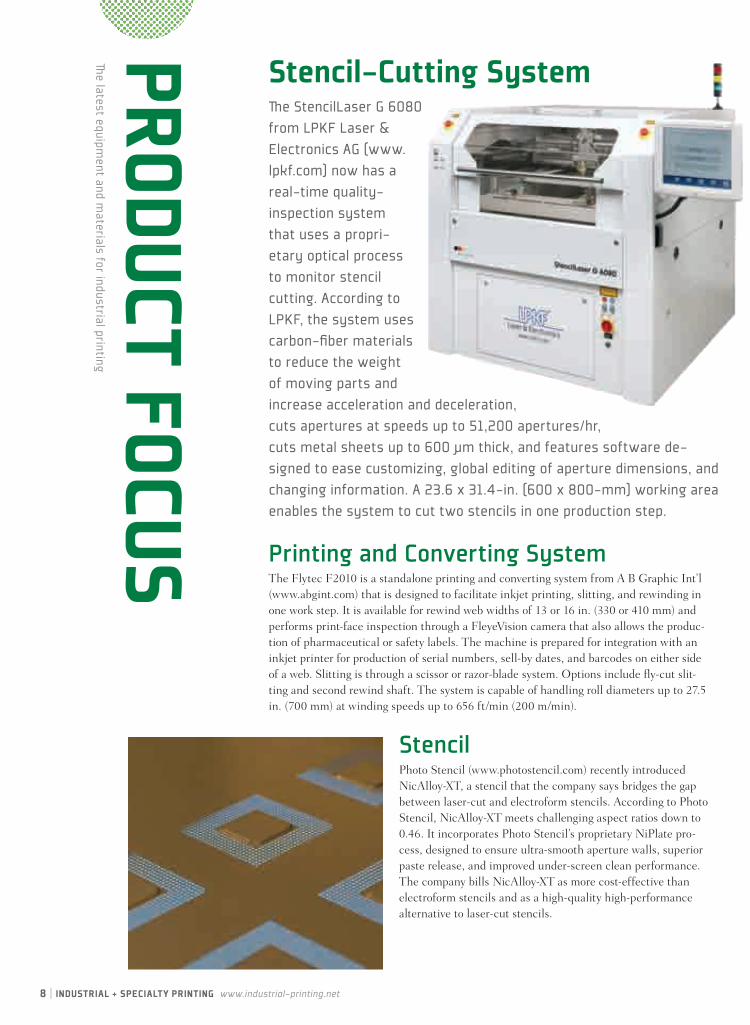
stencil-cutting systemThe StencilLaser G 6080 from LPKF Laser & Electronics AG (www.lpkf.com) now has a real-time quality- inspection system that uses a propri-etary optical process to monitor stencil cutting. According to LPKF, the system uses carbon-fiber materials to reduce the weight of moving parts and increase acceleration and deceleration, cuts apertures at speeds up to 51,200 apertures/hr, cuts metal sheets up to 600 μm thick, and features software de-signed to ease customizing, global editing of aperture dimensions, and changing information. A 23.6 x 31.4-in. (600 x 800-mm) working area enables the system to cut two stencils in one production step.
product focusTh
e latest equipment and m
aterials for industrial printing
Printing and Converting SystemThe Flytec F2010 is a standalone printing and converting system from A B Graphic Int’l (www.abgint.com) that is designed to facilitate inkjet printing, slitting, and rewinding in one work step. It is available for rewind web widths of 13 or 16 in. (330 or 410 mm) and performs print-face inspection through a FleyeVision camera that also allows the produc-tion of pharmaceutical or safety labels. The machine is prepared for integration with an inkjet printer for production of serial numbers, sell-by dates, and barcodes on either side of a web. Slitting is through a scissor or razor-blade system. Options include fly-cut slit-ting and second rewind shaft. The system is capable of handling roll diameters up to 27.5 in. (700 mm) at winding speeds up to 656 ft/min (200 m/min).
StencilPhoto Stencil (www.photostencil.com) recently introduced NicAlloy-XT, a stencil that the company says bridges the gap between laser-cut and electroform stencils. According to Photo Stencil, NicAlloy-XT meets challenging aspect ratios down to 0.46. It incorporates Photo Stencil’s proprietary NiPlate pro-cess, designed to ensure ultra-smooth aperture walls, superior paste release, and improved under-screen clean performance. The company bills NicAlloy-XT as more cost-effective than electroform stencils and as a high-quality high-performance alternative to laser-cut stencils.

may/june 2011 |
Metallization Paste
Solamet PV701 photovoltaic metallization paste from DuPont Microcircuit Materials (www.dupont.com) is the company’s new-est generation of Metal Wrap Through (MWT) technology for back-side-interconnected silicon-solar-cell designs. According to DuPont, advanced product composition enables the manufacture of back-contact-cell designs that deliver up to 0.4% greater conver-sion efficiency for solar cells. DuPont explains that MWT is a specialized cell structure that transfers the bus bars on the front side to the backside, reducing shading on the front side of the cell. The connections are made through holes in the silicon with the same composition as the bus bars. Solamet PV701 is formulated for excellent electrical contact to front-side silver grid structures, high-mechanical strength, low shunting, high-line conductivity, and outstanding solderability as a p-contact metallization.
Overlaminate3M Commercial Graphics (www.3m.com) introduces Scotchcal Gloss Overlaminate 8528. It is designed to withstand harsh envi-ronmental conditions, including extreme temperatures, UV rays, and acid dew. The company has a published warranty of two years for horizontal surfaces and up to seven years for vertical surfaces. The 2-mil cast vinyl is engineered for conformability and dimen-sional stability and is compatible with solvent, latex, and UV inks. Sample rolls are available.
Stencil
FCT Assembly (www.fctassembly.com) recently debuted Ultra-Slic Stencil with Nano-Coating. The company says the addition of nano-coating to UltraSlic further increases the performance gap between it and any other stencil technology available today. According to FCT, the addition of a permanent, hydrophobic nano-coating to the UltraSlic stencil foil minimizes the ability of solder paste to stick to the stencil apertures and the bottom side of the foil. The nano-coating is engineered to facilitate up to a 10X increase in the number of prints before cleaning the stencil, as well as successful printing at surface-area ratios below 0.45. The company notes that UltraSlic FG stencils have lower standard deviations, higher repeatability, and cleaner release of solder paste compared to other stencil technologies.
Upgraded Cylinder Screen PressSakurai (www.sakurai.com) has updated its Maestro MS-80SD Cylinder Screen Press with an optical camera-registration system with monitor, laser-positioning assist for screen-frame changes, and a numerical-indication system designed to improve registra-tion and performance. The Maestro MS-80SD supports media up to 31.625 x 21.75 (800 x 550 mm) and 0.001-0.031 in. (0.05-0.8 mm) thick, a maximum print size of 28.375 x 19.75 in. (720 x 500 mm), and print speeds of 100-2000 impressions/hr.
Flexo PressK2 Int’l (www.k2flexo.com) offers its FA Fast Action flexo press in seven con-figurations. Models range from six to 12 colors, 10- to 25-in. (255- to 635-mm) maximum cutting-die widths, 10.25- to 32-in. (260- to 820-mm) maximum printing widths, one or two product rewinders, and maximum print speeds of 495 ft/min (150 m/min). Standard equipment includes PLC touch-screen controls, automatic web tension, print and die stations of equal height, ceramic anilox rolls, and more. Options include rotary cold-foil stamping, UV laminating, sheeting, fan folding, and video web inspection.
Optical Registration SystemSystematic Automation Inc. (www.systauto.com) has introduced a mod-ular optical registration system for screen printing on glass, plastic, or stainless-steel bottles. The first color is printed randomly or in relation to a bottle seam. Subsequent colors are printed in relation to the first color. The sensor uses servo technology to find the leading edge of the first image, and Systematic Automation reports sensor accuracy of ±0.002 in.
(±0.05 mm). This device is designed for use on any semiautomatic screen press, including Systematic Automation’s Model F-1 DC.
10 | IndustrIal + specIalty prIntIng www.industrial-printing.net
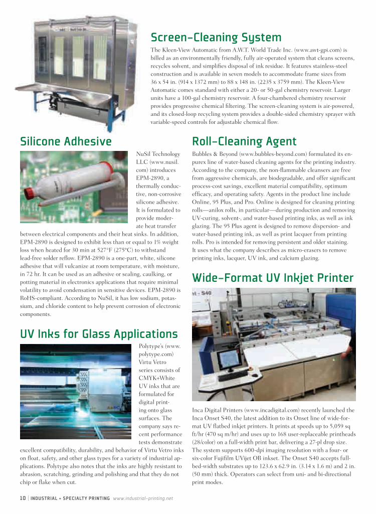
Screen-Cleaning SystemThe Kleen-View Automatic from A.W.T. World Trade Inc. (www.awt-gpi.com) is billed as an environmentally friendly, fully air-operated system that cleans screens, recycles solvent, and simplifies disposal of ink residue. It features stainless-steel construction and is available in seven models to accommodate frame sizes from 36 x 54 in. (914 x 1372 mm) to 88 x 148 in. (2235 x 3759 mm). The Kleen-View Automatic comes standard with either a 20- or 50-gal chemistry reservoir. Larger units have a 100-gal chemistry reservoir. A four-chambered chemistry reservoir provides progressive chemical filtering. The screen-cleaning system is air-powered, and its closed-loop recycling system provides a double-sided chemistry sprayer with variable-speed controls for adjustable chemical flow.
Silicone AdhesiveNuSil Technology LLC (www.nusil.com) introduces EPM-2890, a thermally conduc-tive, non-corrosive silicone adhesive. It is formulated to provide moder-ate heat transfer
between electrical components and their heat sinks. In addition, EPM-2890 is designed to exhibit less than or equal to 1% weight loss when heated for 30 min at 527°F (275ºC) to withstand lead-free solder reflow. EPM-2890 is a one-part, white, silicone adhesive that will vulcanize at room temperature, with moisture, in 72 hr. It can be used as an adhesive or sealing, caulking, or potting material in electronics applications that require minimal volatility to avoid condensation in sensitive devices. EPM-2890 is RoHS-compliant. According to NuSil, it has low sodium, potas-sium, and chloride content to help prevent corrosion of electronic components.
Roll-Cleaning AgentBubbles & Beyond (www.bubbles-beyond.com) formulated its en-purex line of water-based cleaning agents for the printing industry. According to the company, the non-flammable cleansers are free from aggressive chemicals, are biodegradable, and offer significant process-cost savings, excellent material compatibility, optimum efficacy, and operating safety. Agents in the product line include Online, 95 Plus, and Pro. Online is designed for cleaning printing rolls—anilox rolls, in particular—during production and removing UV-curing, solvent-, and water-based printing inks, as well as ink glazing. The 95 Plus agent is designed to remove dispersion- and water-based printing ink, as well as print lacquer from printing rolls. Pro is intended for removing persistent and older staining. It uses what the company describes as micro-erasers to remove printing inks, lacquer, UV ink, and calcium glazing.
Wide-Format UV Inkjet Printer
Inca Digital Printers (www.incadigital.com) recently launched the Inca Onset S40, the latest addition to its Onset line of wide-for-mat UV flatbed inkjet printers. It prints at speeds up to 5,059 sq ft/hr (470 sq m/hr) and uses up to 168 user-replaceable printheads (28/color) on a full-width print bar, delivering a 27-pl drop size. The system supports 600-dpi imaging resolution with a four- or six-color Fujifilm UVijet OB inkset. The Onset S40 accepts full-bed-width substrates up to 123.6 x 62.9 in. (3.14 x 1.6 m) and 2 in. (50 mm) thick. Operators can select from uni- and bi-directional print modes.
UV Inks for Glass ApplicationsPolytype’s (www.polytype.com) Virtu Vetro series consists of CMYK+White UV inks that are formulated for digital print-ing onto glass surfaces. The company says re-cent performance tests demonstrate
excellent compatibility, durability, and behavior of Virtu Vetro inks on float, safety, and other glass types for a variety of industrial ap-plications. Polytype also notes that the inks are highly resistant to abrasion, scratching, grinding and polishing and that they do not chip or flake when cut.
may/june 2011 | 11
Analysis Solution for Flexo Printing
The Betaflex Pro from Beta Industries (www.betascreen.com) is an analysis solution for flexo printing that includes software and hardware designed to assess small highlight dots and advanced surface treatments. According to the company, Betaflex Pro’s 3D Dot Structure Imaging, operating at 22,000 pixels/in., delivers numerical analysis and visual confirmation of these small halftone dots in such a way that operators are no longer left guess-ing or making subjective judgments. Beta Industries explains that 2D imaging of the full tonal range occurs at 14,000 pixels/in., yielding precise and repeatable measure-ments from 50- to 200-line/in. convention-al and FM screens. Production samples are imaged with a topographical visualization and comparison function, in addition to a numerical readout. The system gener-ates pass, warning, or fail indicators to guide the operator in accepting or rejecting plates.
UV CoaterTEC Lighting (www.teclighting.com) recently unveiled the XB18, a system the company bills as the industry’s first double-sided UV coater. The XB18 offers on-the-fly shifting between single- and double sided coating, and the coatings can be varied. For example, a production manager can choose a satin coating on one side of the sheet and gloss on the other. The XB18 also can be arranged inline with a digital press. Standard configurations for the ini-tial offering include 18-in.-wide (457-mm) handfed, auto-feeder, and inline presses. According to TEC Lighting, 40-in.-wide (1016-mm) models are scheduled for future release.
Send uS your product newS! email [email protected]

12 | IndustrIal + specIalty prIntIng www.industrial-printing.net
busIness m
anagement
making product eco-compliance easy
In today’s global market, equipment companies need not only know about safety, performance, and quality, but they also need to keep an eye on the amount of hazardous substances contained within the final product. Many industrialized countries and areas have restricted the use of certain hazardous substances in equipment.
In 2006, product environmental com-pliance in the electronics industry began with the EU’s Restriction on the use of certain Hazardous Substances in electri-cal and electronic equipment Directive (commonly referred to as RoHS). RoHS is in a state of change, as documented in Table 1. Companies were busy gathering documents and data-information sheets on whether or not a part contained the restricted six substances: lead, mercury, hexavalent chromium, cadmium, poly-bro-minated biphenyls (PBBs), and poly-bromi-nated biphenyl ethers (PBDEs). Compa-nies did not focus on this task as a process, but as a once-and-done project. In 2007, when China released its version of RoHS for electronics, the requirements were dif-ferent, as were the products covered; and companies scrambled to make changed to their projects to meet the new require-ments. In addition to the RoHS–type requirements, companies also need to know about the reporting requirements for regulations such as EU REACH.
In 2008, with the introduction of EU’s Registration, Evaluation, Authorization and registration of CHemicals regulation (REACH), the list of substances increased
Krista CrottyAlberi EcoTech
to more than double the number of sub-stances in the RoHS Directive; with the potential to exceed thousands of reportable substances. Nowadays, with every country looking at its own list, where do you start? Companies must look at the big picture now and treat product environmental compliance as a process, not a project. Companies should focus on how all the countries and various legislations paint a total picture, not just focus on each indi-vidual country and its legislation. An audit of the product-environmental-compliance program does just this. The company saves money by taking the insight and direction from an audit.
Understanding, tracking, and meeting the multiple environmental requirements around the world, without driving yourself crazy, is a daunting task. Companies typi-cally focus too much on the details and not the overall picture. Additionally, com-
panies focus on the individual countries as individual projects, when they should be looking at the matrix of countries and requirements—finding the lowest common denominator and creating a process for compliance.
the audIt processIn today’s market, companies not only need to concern themselves with govern-ment enforcement, but also customer requirements. Customers are now looking for information on the products they are purchasing. A customer audit or inquiry can be more tasking than a government enforcement audit. Why? Because a customer looks at a matrix of parts and legislation, not one product or one legisla-tive requirement.
So where does one start with determin-ing compliance? Perform an audit. Audit the entire product-environmental-compli-
Action / Event Date / TimelineApproval by EC of RoHS Recast Directive translated into all languages March 2011
Publication into EC Official Journal April/May 2011
Directive Entry into Force +20 days
Member State deadline for transposition into National Law +18 months
Estimated enforcement date by Member States November 2012
* Dates may change, dates as of information March 2011
Table 1 Estimated timetable for the RoHS recast. Dates are subject to change.

may/june 2011 | 13
ance process. Focus on three things initial-ly: awareness, preparation, and execution. Review how you are approaching compli-ance instead of taking stock and reviewing every data sheet for every component that makes up a product. When assessing a program, consider:
• Listing of products, distribution regions, and type of distribution in each region
• Listing of legislation in those areas, which eases the process of determining where a program falls short and in cross-referencing requirements so project tasks are not duplicated
• How the company or a company repre-sentative keeps abreast of legislation and changes in the legislation (tracking news and happenings through industry groups or standards organizations allows for cross-pollination of best practices from others in the industry)
• Whether there is a company lead respon-sible for answering questions about the program and whether there is a listing of
team members supporting this lead• Where the program information is
stored and how program information is organized
• Whether the program gives a sense of progressive understanding and adjust-ment or a sense of panic and fire fighting
If you are facing a government audit or customer inquiry, be responsive, anticipate questions, and assume nothing. Product-environmental-compliance legislation and customer requirements change continu-ously. Having an eco-compliance program for products that does the same is critical to continued success. Sharing your plan, execution of that plan, and a general knowledge of the requirements will lessen the corrective actions from an audit or inquiry.
Are you sure you have implemented your eco-compliance program success-fully? If not, consider a mock audit to get an outside opinion. A mock audit is simple. Someone unfamiliar with the program
looks under the hood to see whether they can understand the basic information about the program. The mock auditor re-views your program and attempts to answer the questions listed above and determine whether you’ve executed a describable, detailed plan that showing the program meets stated requirements.
Krista Crotty holds a B.S. in mechanical engi-neering and an M.S. in production and operations management. She is the chief eco-geek and managing partner of Alberi EcoTech located in Las Vegas, NV, USA. Krista’s experience crosses aerospace, semiconductor-manufacturing equipment, electrical-component technology and reliability, and motorsports preparation and competition.
krista crottyAlberi EcoTech
The right price.
From the benchtop to ourlargest unit, Xenon Sinteronsystems cost a fraction ofcompetitive solutions, whileoffering the features youneed.
The right company.
Xenon has pioneered the useof photonic curing in numerousindustries. Now we’re using ourexperience to revolutionizesintering for heat-sensitiveflexible circuits.
The right systems.
Need to sinter copper or silverink on flexible substrates?Choose from our family ofSinteron systems to matchyour research and develop-ment needs.
SINTERON 500
Linear Stage Unit
Scan this QR codewith your smart phoneto see the video.
See our videoThe Future of Flexible Printed Circuits Learn more about our low-
temperature sintering solutions atwww.xenoncorp.com/sinter
For the lab and beyond.
SINTERON 2000
Membrane Switch and Touchscreen Basics
The design, prototype, and production processes for a user interface occur at several distinct stages of product development for original equipment manufacturers (OEMs). Typically, the in-house engineer-ing and marketing team of the OEM coordinate the functional and aesthetic requirements for the user interface. These design require-ments are then coordinated with the OEM’s contract manufacturer if that is how their assembly normally proceeds. It is very important to allow suf cient time for this process to include changes and prototype stages. Design consultations and a review of material choices and assembly options can reduce costs and assist in compliance with any special requirements, such as environmentally friendly materials.
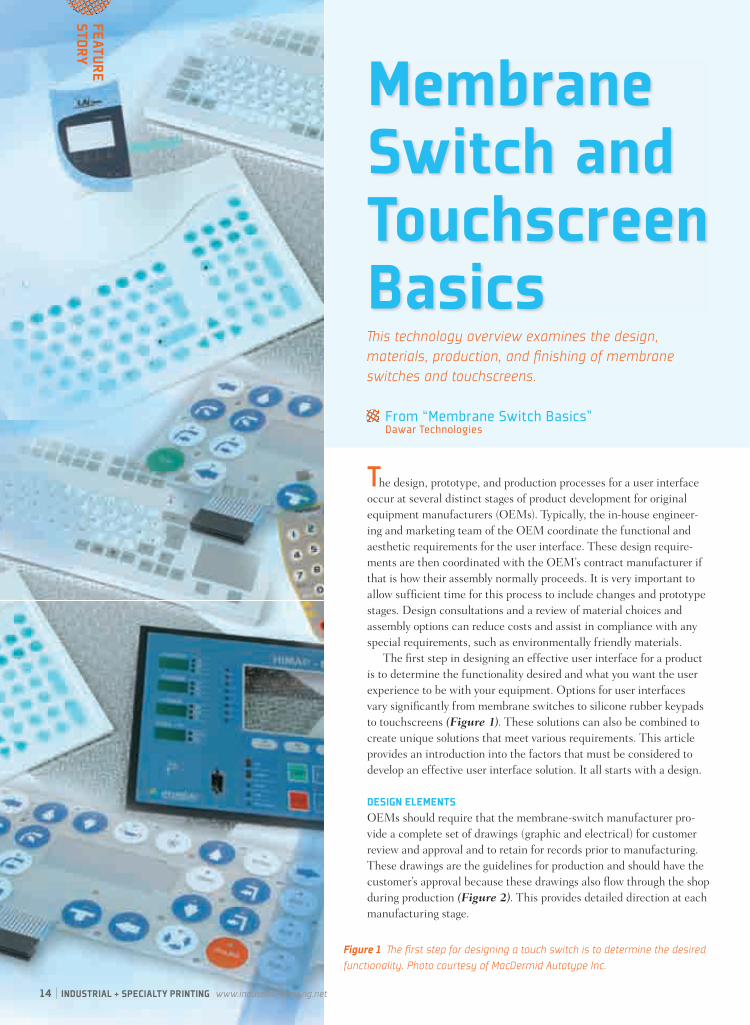
The rst step in designing an effective user interface for a product is to determine the functionality desired and what you want the user experience to be with your equipment. Options for user interfaces vary signi cantly from membrane switches to silicone rubber keypads to touchscreens (Figure 1). These solutions can also be combined to create unique solutions that meet various requirements. This article provides an introduction into the factors that must be considered to develop an effective user interface solution. It all starts with a design.
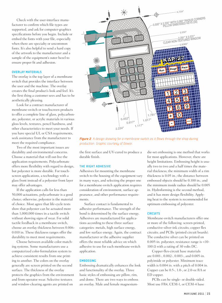
DESIGN ELEMENTSOEMs should require that the membrane-switch manufacturer pro-vide a complete set of drawings (graphic and electrical) for customer review and approval and to retain for records prior to manufacturing. These drawings are the guidelines for production and should have the customer’s approval because these drawings also ow through the shop during production (Figure 2). This provides detailed direction at each manufacturing stage.
is technology overview examines the design, materials, production, and fi nishing of membrane switches and touchscreens.
From “Membrane Switch Basics”Dawar Technologies
14 | INDUSTRIAL + SPECIALTY PRINTING www.industrial-printing.net
FEATURE STORY
Figure 1 e fi rst step for designing a touch switch is to determine the desired functionality. Photo courtesy of MacDermid Autotype Inc.
MAY/JUNE 2011 | 15
Membrane Switch and Touchscreen Basics
Check with the user-interface manu-facturer to con rm which le types are supported, and ask for computer-graphics speci cations before you begin. Include or embed the fonts with your le, especially when there are specialty or uncommon fonts. It’s also helpful to send a hard copy of the artwork to the manufacturer and a sample of the equipment’s outer bezel to ensure proper t and adhesion.
OVERLAY MATERIALSThe overlay is the top layer of a membrane switch that provides the interface between the user and the machine. The overlay creates the nal product’s look and feel. It’s the rst thing a customer sees and has to be aesthetically pleasing.
Look for a contract manufacturer of membrane-switch or touchscreen products to offer a complete line of glass, polycarbon-ate, polyester, or acrylic materials in various gloss levels, textures, pencil hardness, and other characteristics to meet your needs. If you have special UL or CSA requirements, seek assistance from the manufacturer to meet the required compliance.
Two of the most important issues are durability and environmental concerns. Choose a material that will out-live the application requirements. Polycarbonate offers more exibility with regard to design, but polyester is more durable. For touch-screen applications, a technology with a glass front instead of a polyester front layer may offer advantages.
If the application calls for less than 50,000 actuations, polycarbonate is a good choice; otherwise, polyester is the material of choice. Most agree that life-cycle tests show that polyester can be actuated more than 1,000,000 times in a tactile switch without showing signs of wear. For solid tactile feedback in a membrane switch, choose an overlay thickness between 0.006-0.010 in. These thickness ranges offer the durability to meet most requirements.
Choose between available color-match-ing systems. Some manufacturers use a computerized color-formulation system to achieve consistent results from one print-ing to another. The colors on the overlay generally are screen printed on the second surface. The thickness of the overlay protects the graphics from the environment and from operator wear. Selective textures and window-clearing agents are printed on
the rst surface and UV-cured to produce a durable nish.
THE RIGHT ADHESIVEAdhesives for mounting the membrane switch to the housing of the equipment vary in many ways, and selecting the proper one for a membrane-switch application requires consideration of environment, surface ap-pearance, and other performance require-ments.
Surface contact is fundamental to adhesive performance. The strength of the bond is determined by the surface energy. Adhesives are manufactured for applica-tions according to these three surface categories: metals, high surface energy, and low surface energy. Again, the contract manufacturer or the adhesive supplier offers the most reliable advice on which adhesive to use for each membrane-switch application.
EMBOSSINGEmbossing dramatically enhances the look and functionality of the overlay. Three basic styles of embossing are pillow, rim, and dome. There are two ways to emboss an overlay. Male and female magnesium-
die-set embossing is one method that works for most applications. However, there are height limitations. Embossing height is usu-ally two to two and a half times the mate-rial thickness; the minimum width of a rim thickness is 0.05 in.; the distance between embossed objects should be 0.100 in.; and the minimum inside radius should be 0.005 in. Hydroforming is the second method, and it has more design exibility. Apply-ing heat to the system is recommended for optimum embossing of polyester.
CIRCUITSMembrane-switch manufacturers offer one or more of the following: screen-printed, conductive-silver-ink circuits; copper ex circuits; and PCBs (printed circuit boards). The conductive silver can be printed on 0.005-in. polyester, resistance range is <10-100 Ω with a rating of 30 volts DC.
Copper- ex-circuit base materials are 0.001-, 0.002-, 0.003-, and 0.005-in. polyimide or polyester. Minimum trace width is 0.004 in. with a pitch of 0.004 in. Copper can be 0.5-, 1.0-, or 2.0-oz RA or ED copper.
PCBs can be single- or double-sided. Most use FR4, CEM-1, or CEM-4 base
Figure 2 A design drawing for a membrane switch as it fl ows through the shop during production. Graphic courtesy of Dawar.
0.500" X 0.335" WITH 0.060" RADIUS CORNERS
PILLOW EMBOSSED KEYS (3X)
0
2.234"
4.724"
.433"
.868"
1.303"
1.738"
3.532"
2.8385"
0.617"1.117"
1.617"0.452"1.781"
2.291" X 0.531"
CLEAR NON-TEXTURED WINDOW

16 | IndustrIal + specIalty prIntIng www.industrial-printing.net
material. The minimum trace width for gold is 0.003 in. for hot-air leveling of 0.006 in. Plating thickness can be 1-25 µm. Plating options include copper, carbon, nickel, or gold.
Embedded electronics, such as LEDs and resistors, are placed using surface-mount technology, either via in-house pick-and-place machines or outside purchased. The surface-mounted device (SMD) adheres to the circuit layer with conductive epoxy and is typically encapsulated with a UV-cured polyurethane.
shIeldIngSeek the advice of the manufacturer on the proper shielding to meet the ESD, EMI, or RFI requirements. There are two common methods of shielding. The first is by using copper or aluminum foil with or without laminated polyester to the second surface. The second method uses screen-printed conductive silver ink in a grid or complete coating of the first surface. The shield can be terminated by three methods: tab, which can be attached to a stud or standoff on the metal backer or the metal enclosure;
connector, which allows the shield to terminate into the pins of the mem-brane-switch tail; and wraparound, where the shield layer wraps around the membrane switch and grounds to the enclosure.
tactIle and non-tactIle membrane swItchesNon-tactile membrane switches can be designed with a wide range of actua-tion forces. The actuation force is determined by circuit spacer thickness. If required, a non-tactile membrane switch can be designed as thin as 0.21 in.
Tactile mem-brane switches (Figure 3) incorporate a metal dome or a polydome to achieve the desired tactile response. Using different sizes of metal domes or polydomes varies actuation force. Metal domes come in a large variety of shapes and sizes with actua-tion forces between 180-700 g. Different polydome actuation forces can be achieved by changing the diameter and height of the polydome to meet requirements.
touchscreen basIcsMany products that may traditionally have been operated with membrane switches now have those capabilities provided with touchscreen products to provide a complete front-panel assembly. The touchscreen has several advantages over other computer devices. Unlike moving a mouse, swiveling a joystick, or pushing a key in a membrane switch to perform a desired function indi-rectly, users can simply touch an object on a screen. Touchscreens have no moving parts and, therefore, are durable and appropriate
for frequent use in unlimited applications. A touchscreen can also be operated with a countless menu of screens for which each touch point on the screen can cause the equipment to respond in different ways, un-like the defined position and functionality of a membrane-switch key (Figure 4).
The main components of a touchscreen that allow users to operate a device simply by touching an optically clear sensor directly in front of the display screen include the touchscreen sensor, controller, and software driver. The sensor typically is a glass panel with a touch-responsive surface. The controller is a PCB acting as an interface between the sensor and the display. The controller takes information from the touchscreen and translates it into information a computer can understand. The software driver is a computer program that allows the operating system and the controller to communicate and helps the computer recognize input.
There are many types of touchscreens. One of the oldest and most common tech-nologies is the four-wire resistive touch-screen. The four-wire resistive touchscreen comprises a conductive bottom layer of either glass or film and a conductive top film layer, separated by small, transparent spacer dots. Voltage is applied across the conductive surface. Any type of probe, fin-ger, gloved finger, credit card, pen, or stylus can be used to apply pressure against the top film to activate the screen. When ample touch pressure is applied to the top layer, the film flexes inward and makes contact with the bottom layer, resulting in a voltage drop. This change in voltage is detected by the controller. By alternating the voltage signal between the top and bottom layer, the X and Y coordinates of the user’s touch are computed.
In a film-on-glass (FG) construction, the bottom layer is an ITO-coated glass. In a polyester laminated (PL) or film-film-glass construction, the bottom conductive layer is also polyester. An additional layer of optically clear adhesive (OCA) bonds the bottom polyester layer to a backer typically made of glass or poly material.
editor’s note: This article was created from information excerpted from Dawar Technologies, “Membrane Switch Basics” and in “Touchscreen Basics.” For more information about the source, visit www.dawar.com.
Figure 3 (above) Examples of custom tactile membrane switches. Photo courtesy of MacDermid Autotype Inc. Figure 4 (right) Touchscreens come in many formats from desktop computer screens to handheld smart phones.
HOW MEMBRANE-SWITCH FILMS ARE USED
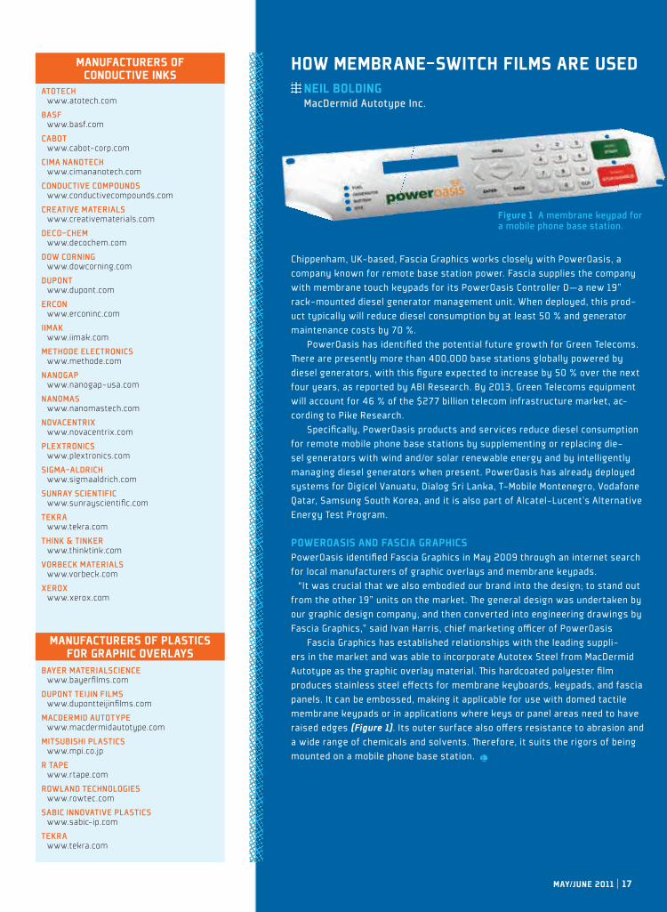
Chippenham, UK-based, Fascia Graphics works closely with PowerOasis, a company known for remote base station power. Fascia supplies the company with membrane touch keypads for its PowerOasis Controller D—a new 19” rack-mounted diesel generator management unit. When deployed, this prod-uct typically will reduce diesel consumption by at least 50 % and generator maintenance costs by 70 %.
PowerOasis has identifi ed the potential future growth for Green Telecoms. ere are presently more than 400,000 base stations globally powered by diesel generators, with this fi gure expected to increase by 50 % over the next four years, as reported by ABI Research. By 2013, Green Telecoms equipment will account for 46 % of the $277 billion telecom infrastructure market, ac-cording to Pike Research.
Specifi cally, PowerOasis products and services reduce diesel consumption for remote mobile phone base stations by supplementing or replacing die-sel generators with wind and/or solar renewable energy and by intelligently managing diesel generators when present. PowerOasis has already deployed systems for Digicel Vanuatu, Dialog Sri Lanka, T-Mobile Montenegro, Vodafone Qatar, Samsung South Korea, and it is also part of Alcatel-Lucent’s Alternative Energy Test Program.
POWEROASIS AND FASCIA GRAPHICSPowerOasis identifi ed Fascia Graphics in May 2009 through an internet search for local manufacturers of graphic overlays and membrane keypads.
“It was crucial that we also embodied our brand into the design; to stand out from the other 19” units on the market. e general design was undertaken by our graphic design company, and then converted into engineering drawings by Fascia Graphics,” said Ivan Harris, chief marketing offi cer of PowerOasis
Fascia Graphics has established relationships with the leading suppli-ers in the market and was able to incorporate Autotex Steel from MacDermid Autotype as the graphic overlay material. is hardcoated polyester fi lm produces stainless steel eff ects for membrane keyboards, keypads, and fascia panels. It can be embossed, making it applicable for use with domed tactile membrane keypads or in applications where keys or panel areas need to have raised edges (Figure 1). Its outer surface also off ers resistance to abrasion and a wide range of chemicals and solvents. erefore, it suits the rigors of being mounted on a mobile phone base station.
ATOTECHwww.atotech.com
BASFwww.basf.com
CABOTwww.cabot-corp.com
CIMA NANOTECHwww.cimananotech.com
CONDUCTIVE COMPOUNDSwww.conductivecompounds.com
CREATIVE MATERIALSwww.creativematerials.com
DECO-CHEMwww.decochem.com
DOW CORNINGwww.dowcorning.com
DUPONTwww.dupont.com
ERCONwww.erconinc.com
IIMAKwww.iimak.com
METHODE ELECTRONICSwww.methode.com
NANOGAPwww.nanogap-usa.com
NANOMASwww.nanomastech.com
NOVACENTRIXwww.novacentrix.com
PLEXTRONICSwww.plextronics.com
SIGMA-ALDRICHwww.sigmaaldrich.com
SUNRAY SCIENTIFICwww.sunrayscientifi c.com
TEKRAwww.tekra.com
THINK & TINKERwww.thinktink.com
VORBECK MATERIALSwww.vorbeck.com
XEROXwww.xerox.com
BAYER MATERIALSCIENCEwww.bayerfi lms.com
DUPONT TEIJIN FILMSwww.dupontteijinfi lms.com
MACDERMID AUTOTYPEwww.macdermidautotype.com
MITSUBISHI PLASTICSwww.mpi.co.jp
R TAPEwww.rtape.com
ROWLAND TECHNOLOGIESwww.rowtec.com
SABIC INNOVATIVE PLASTICSwww.sabic-ip.com
TEKRAwww.tekra.com
MANUFACTURERS OF PLASTICS FOR GRAPHIC OVERLAYS
MANUFACTURERS OF CONDUCTIVE INKS
Figure 1 A membrane keypad for a mobile phone base station.
MAY/JUNE 2011 | 17
NEIL BOLDINGMacDermid Autotype Inc.
18 | IndustrIal + specIalty prIntIng www.industrial-printing.net
ABRASION RESISTANCEAbility to resist surface wear.
ACCELERATED AGING A test method that simulates long-term environmental effects.
ADHESION The molecular force of attraction between unlike materials. The strength of attraction is determined by the surface energy of the material. The higher the surface energy, the greater the molecular attraction. The lower the surface energy, the weaker the attractive force.
AMPERE (AMP) A standard unit of current. Defined as the amount of current that flows when one volt of EMF is applied across one ohm of resistance. An ampere of current is produced by one coulomb of charge passing a point in one second.
AQLAcceptable quality level.
ASTM American Society for Testing and Materials International.
AUTOTEX Trademark for textured polyester graphic overlay film from MacDermid Autotype Ltd.
BOND STRENGTHAmount of adhesion between two surfaces.
BREAKDOWN VOLTAGE The voltage at which the insulation between two conductors is destroyed.
CAD/CAM Computer-aided design/computer-aided manufacturing.
CAPACITANCE The property of conductors and dielectrics that allows the storage of an electrical charge when voltage is applied. See ASTM F1663-95.
CARBON/GRAPHITE INKS Specially prepared suspensions of carbon black. These systems are used for lowering cost when the conductivity of a metal base system is not required. Often printed over silver circuitry to reduce the potential for silver migration. Also used for printed resistors.
CERTIFICATE OF COMPLIANCE (C OF C) A certificate generated by a quality control department confirming that the product being shipped meets the manufacturing document.
CONDUCTIVITY The ability of a material to allow electrons to flow measured by the current per unit of voltage applied.
CONTACT BOUNCE Intermittent contact opening and closure that may occur after switch operation. See ASTM F161-95.
CSACanadian Standards Association.
CURRENT, ALTERNATING (AC) An electric current that periodically reverses direction of the electron flow. The rate at which a full cycle occurs in a given unit of time (usually a second) is called the frequency of the current.
CURRENT, DIRECT (DC) Electrical current whose electrons flow in one direction only. It may be constant or pulsating as long as its movement is in the same direction.
MeMbrane swItch and touchscreen basIcs glossary of terMs
DEAD FRONT Cosmetic feature of a graphic overlay allowing for a display feature to be visible only when backlit.
DIE CUTTING Process for blanking or cutting sheet or roll materials to predetermined shapes for membrane switch components, graphic overlays, and labels.
DIELECTRICAn insulating (non-conducting) medium.
DOME RETAINER An adhesive layer designed to hold metal domes in keys.
EL LAMPS A thin (0.010- to 0.025-in.) illuminating devices used to light large areas, commonly used in LCD, control panel, and membrane switch backlighting.
EMBEDDED LEDThe practice of encapsulating a surface-mount LED into a membrane switch construction.
EMBOSSMechanical and thermoforming of graphic features, providing a raised feature for accenting key surfaces, logos and to allow for embedding of surface-mount LEDs within the switch.
EMBOSS, RAILCreates a raised ridge around the perimeter of the key area.
EMBOSS, PILLOWCreates a raised surface in the graphic overlay over the entire key area.
EMI/RFI/ESD SHIELDPrinted conductor pattern or separate aluminum or copper film employed in membrane switch designs to reduce the effects of electromagnetic and radio frequency interference.
FIBEROPTIC BACKLIGHTINGIlluminating device used to light large areas. Strands of clear fiber are woven and bundled, after polishing the fiber ends are illuminated by an LED or halogen lamp.
FLAT FLEX CONNECTOR (FFC)Connector type commonly used to terminate membrane switch circuitry.
FONT A set of characters having a unified design.
GLOSS LEVELThe degree of shininess of a substrate, usual specified in percentages, for example, 75% gloss, 90% gloss.
HB-94HBUnderwriters Laboratories flame-retardant specification (horizontal burn).
HSEHigh surface energy.
INSERT LEGEND (INSERT GRAPHICS)A design feature allowing for changes to nomenclature and symbols by the client or end user. The feature is accomplished by creating a pocket in the membrane switch assembly to allow for an insert card.
INTERNALLY VENTEDSwitch openings are connected to each other but not to the outside atmosphere. This design approach is used to seal the switch from moisture and contaminants.
ISOInternational Organization for Standardization. Known for the development of a series of standards called ISO 9000 for developing Total Quality Management, and creating a continuous Quality Improvement Process.
ITOIndium tin oxide, a thin-film conductive material vacuum deposited on the surface of a film substrate. Material is often the base material for resistive touchscreens.
KEY HEIGHTThe measured distance from the bottom (base) of the keypad to the top surface of the key.
KEY TRAVELThe distance a switch moves to close an electrical contact, expressed in inches or MM.
LEDLight-emitting diode.
LEXANSabic, formerly General Electric registered trademark for polycarbonate film.
LSELow surface energy.
MEMBRANE SWITCHA momentary switching device in which at least one contact is on or made of a flexible substrate.
METAL DOMEStainless-steel disc or element. One of several approaches used to produce tactile response.
MOISTURE RESISTANCEThe ability of a material to resist absorbing moisture from the air or after immersion in water.
MP Modified performance. An adhesive classification of 3M products.
MUNSELLColor-matching system that defines color by three attributes: hue, value, chroma. Fifteen hundred color samples are available as opaque pigmented films.
MYLARDuPont trademark for polyethylene terephthalate (polyester) film.
NEMANational Electrical Manufacturers Association.
NON-TACTILEMembrane switch constructed without snap action.
OHMThe electrical unit of resistance. The value of resistance through which a potential difference of one volt will maintain a current of one ampere.
OVERLAYDecorative front layer of a membrane switch or control panel.
OVER-TRAVELThe additional travel of a rubber keypad or metal dome after making contact with the circuit.
PANTONE MATCHING SYSTEM (PMS)Color-matching system originally developed for the offset printing industry, commonly used in the membrane switch industry for its broad acceptance, range of colors, and ease of use.
PCBPrinted circuit board.

may/june 2011 | 19
PINOUTThe schematic describing the circuit-output requirements for a membrane switch or another electronic device.
POLYCARBONATEGraphic-overlay film wide used for control panels.
POLYESTER DOMEA spherically formed element in polyester circuit material to provide tactile response in membrane switches. Usually the domes are formed in arrays or sets to match the key configuration of the keypad.
POLYESTERBi-axially oriented polyethylene terephthalate film (PET).
PRESSURE SENSITIVEAdhesive materials that bond with the application of pressure alone and do not require activation by heat or solvents.
RESISTANCEIn DC circuits, the opposition a material offers to current flow, measured in Ohms.
RFI Radio-frequency interference
SCREEN PRINTINGPrint process using mesh stretched over a frame, allowing ink to selectively pass through by using a stencil. The process commonly used for producing graphic overlays and membrane-switch circuits.
SECOND-SURFACE PRINTEDInks are applied to the non-exposed side of the film to allow for the film to protect the inks from scratches or other damage.
SELECTIVE TEXTURINGThe creation of surface effects on matte or gloss films normally applied using the screen-printing process.
SILICONE RUBBERRubber made from silicone elastomers and noted for its retention of flexibility, resilience, and tensile strength over a wide temperature range.
SILVER INKSSpecially prepared suspensions of finely milled silver particles in a variety of resin systems used to produce conductive patterns on flexible substrates.
SPACER An adhesive layer of a membrane switch used to separate circuit layers and to provide key openings allowing for conductors to contact each other when depressed.
STATIC SHIELDPrinted conductor pattern or separate aluminum or copper film used in membrane-switch designs to reduce the effects of static discharges.
STEEL RULE DIEConsists of a 0.750- to 0.875-in.-thick die-board of plywood construction with 0.37-in.-high knives inserted into laser-cut grooves.
TACTILE SWITCHA switch or switch assembly providing a positive snap-action response. The response can be achieved through the use of stainless-steel domes embedded in the membrane switch or polyester domes formed in either the circuit or graphic-overlay layers.
THIXOTROPHYThe property of becoming fluid when disturbed, as by shaking.
VISIBLE LIGHT TRANSMISSIONThe ratio of the amount of total visible solar energy (370-780 nm) that is allowed to pass through a filter, to the amount of total solar energy falling on that filter.
WATTA unit of electrical power that is equivalent to the power represented by 1 amp of current with a pressure of 1 volt in a DC circuit.
ZIFZero insertion force.
membrane switCh and touChsCreen basiCs Glossary of terms
ATLANTA: 888-530-3988BOSTON: 888-530-3986
CHICAGO: 888-530-3985LOS ANGELES: 888-530-3987www.m imak iusa . comFor inquiries outside the USA: Mimaki Engineering Co., Ltd. • 2182-3 Shigeno-otsu, Tomi-city, Nagano 389-0512 Japan • Ph: +81-268-64-2281 Fx:+81-268-64-2285 www.mimaki.co.jp
© 2010, Mimaki USA, Inc. • 150 Satellite Blvd., NE, Suwanee, GA 30024-7128, USA Fx: 678-730-0200
Giving you more options per square inch...
...because more is what we do.
The UJF-706 is a newly developed, higher speed UV curingflatbed printer for industrial applications.
u Prints on substrates up to 5.9” thick including non-coated.u Vivid prints on transparent materials with white ink
underprint function.u Uses hard or flexible inks.u Four point optical positioning recognition system;
1200x1200 dpi resolution.u Satellite drop-free printing with Spray Suppressor System.u Optional roll media printing.
Industrial UV Flatbed
INDUSTRIALPRODUCTS
ULTRA-HIGHRESOLUTION
LOW VOCUV INKS
FLATBEDAPPLICATION
more performance, more resolution, more vibrant color, more versatility,more choices, more speed,
APPLICATIONS: • POP & POS Displays• Promotional Products• Packaging Proofs &
Prototypes• Industrial Applications
& Signage • Membrane Switches• Nameplates &
Plastic Cards
Mimaki_UJF706_H_ISP10.qxd:Layout 1 4/14/10 3:52 PM Page 1
20 | IndustrIal + specIalty prIntIng www.industrial-printing.net
coverstory
sintering nanoparticle-Based Inks on challenging substrates
Saad AhmedXenon Corp.
Exposure to extreme processing environments is a major roadblock that stands in the way of using thin, temperature-sensitive materials in the production of printed electronics. Discover the ways in which photonic sintering can clear a path to success.
may/june 2011 | 21
We live in a world surrounded by electronics. Even though the technology for manufacturing devices and components has advanced in leaps and bounds, the basic printed circuit board (PCB) has not changed significantly. The process of applying photo resist to a sheet of copper that is fixed on a rigid board and using a photo-lithograph-ic process with a chemical-etch process to create tracks and pads to form interconnects between components is still the most common way of building PCBs.
Conventional PCB creation is a subtractive, multistep process that requires chemicals, is wasteful of copper, and does not lend itself to a high-speed, low-cost solution. In some special cases, flexible or rigid-flex PCBs are used, but they are based on the same principles of standard PCB manufacture but use flexible plastic substrates instead of rigid materials.
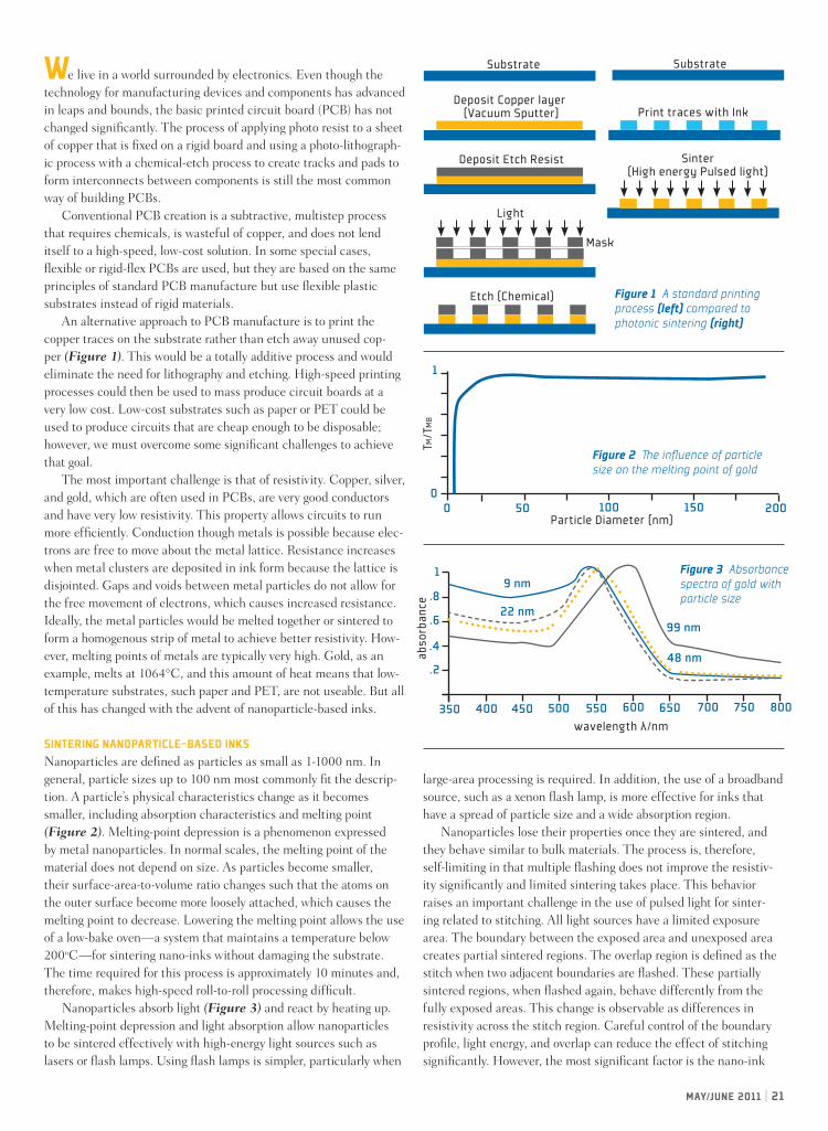
An alternative approach to PCB manufacture is to print the copper traces on the substrate rather than etch away unused cop-per (Figure 1). This would be a totally additive process and would eliminate the need for lithography and etching. High-speed printing processes could then be used to mass produce circuit boards at a very low cost. Low-cost substrates such as paper or PET could be used to produce circuits that are cheap enough to be disposable; however, we must overcome some significant challenges to achieve that goal.
The most important challenge is that of resistivity. Copper, silver, and gold, which are often used in PCBs, are very good conductors and have very low resistivity. This property allows circuits to run more efficiently. Conduction though metals is possible because elec-trons are free to move about the metal lattice. Resistance increases when metal clusters are deposited in ink form because the lattice is disjointed. Gaps and voids between metal particles do not allow for the free movement of electrons, which causes increased resistance. Ideally, the metal particles would be melted together or sintered to form a homogenous strip of metal to achieve better resistivity. How-ever, melting points of metals are typically very high. Gold, as an example, melts at 1064°C, and this amount of heat means that low-temperature substrates, such paper and PET, are not useable. But all of this has changed with the advent of nanoparticle-based inks.
Sintering nanoparticle-baSed inkSNanoparticles are defined as particles as small as 1-1000 nm. In general, particle sizes up to 100 nm most commonly fit the descrip-tion. A particle’s physical characteristics change as it becomes smaller, including absorption characteristics and melting point (Figure 2). Melting-point depression is a phenomenon expressed by metal nanoparticles. In normal scales, the melting point of the material does not depend on size. As particles become smaller, their surface-area-to-volume ratio changes such that the atoms on the outer surface become more loosely attached, which causes the melting point to decrease. Lowering the melting point allows the use of a low-bake oven—a system that maintains a temperature below 200oC—for sintering nano-inks without damaging the substrate. The time required for this process is approximately 10 minutes and, therefore, makes high-speed roll-to-roll processing difficult.
Nanoparticles absorb light (Figure 3) and react by heating up. Melting-point depression and light absorption allow nanoparticles to be sintered effectively with high-energy light sources such as lasers or flash lamps. Using flash lamps is simpler, particularly when
large-area processing is required. In addition, the use of a broadband source, such as a xenon flash lamp, is more effective for inks that have a spread of particle size and a wide absorption region.
Nanoparticles lose their properties once they are sintered, and they behave similar to bulk materials. The process is, therefore, self-limiting in that multiple flashing does not improve the resistiv-ity significantly and limited sintering takes place. This behavior raises an important challenge in the use of pulsed light for sinter-ing related to stitching. All light sources have a limited exposure area. The boundary between the exposed area and unexposed area creates partial sintered regions. The overlap region is defined as the stitch when two adjacent boundaries are flashed. These partially sintered regions, when flashed again, behave differently from the fully exposed areas. This change is observable as differences in resistivity across the stitch region. Careful control of the boundary profile, light energy, and overlap can reduce the effect of stitching significantly. However, the most significant factor is the nano-ink
Substrate Substrate
Deposit Copper layer (Vacuum Sputter)
Deposit Etch Resist
Print traces with Ink
Etch (Chemical)
Light
Mask
Sinter (High energy Pulsed light)
Figure 1 A standard printing process (left) compared to photonic sintering (right)
1
00 50 100 150 200
Particle Diameter (nm)
TM/T
MB
Figure 2 The influence of particle size on the melting point of gold
350 400 450 500 550 600 650 700 750 800
.2
.4
.6
.8
1 Figure 3 Absorbance spectra of gold with particle size
9 nm
22 nm
48 nm
99 nm
wavelength λ/nm
abso
rban
ce

22 | IndustrIal + specIalty prIntIng www.industrial-printing.net
formulation used. Inks designed for multiple flashing generally mitigate the effects of stitching.
Resistivity of sintered inks is generally higher than that of bulk material because of the final material’s remaining poros-ity after sintering. Resistivity values of four to five times that of bulk is considered a good result. Some self-drying inks can achieve resistances of six times bulk. Photonic sintering to date has achieved results ranging between three and five times bulk for certain inks.
Ink formulation plays a major role in photonic sintering. The ink-deposition method must be suited to the ink in terms of viscosity and surface tension. The formulation also determines the drying time for the inks and the adhesion of the ink to the substrate. Photonic sintering performs better with dry ink because pockets of solvent that are trapped in the ink are likely to expand and erupt when exposed to a high-energy light pulse. This causes inks to blow off of the surface, which leads to a reduction in resistivity.
substratesSubstrate selection is another important factor. Interestingly, pa-per and specially coated paper are very good substrates because they can absorb the ink and wick away the carrier agents in the ink. This allows the ink to dry effectively and improves ink adhe-sion. PET and Teflon are also good substrates to use because they are good insulators and, therefore, allow more photonic en-ergy to be absorbed by the ink rather than the substrate. These substrates are often transparent, which means they absorb less light and, in doing so, allow for greater amounts of pulsed-light energy in the sintering process.
Print-related anomalies are less tolerable when dealing with functional inks. Errors in printing can lead to short and open cir-cuits and, if critically located, can render the printed electronic circuit unusable. Ink-layer thickness, which affects resistivity, also becomes more critical.
Most PCBs are based on two or more layers of conduc-tive traces with vias between them. As circuits become more complex, the trace width, gap between traces, and via sizes are made smaller. High-precision printing is required to overcome the challenge. However, multilayer printing on flexible substrates brings an additional problem to the forefront: substrate expan-sion. When PET is used in a roll-to-roll application and is drawn through the printing process, the material is under tension, which causes elastic deformation. Heating the material can increase this single-axis deformation. Failure to account for this deformation leads to mismatched layers and a loss of connectivity.
Placement of ICs and other components is another consid-eration when working with low-temperature, flexible surfaces. Soldering, which is the traditional method of connecting devices to PCBs, is less suited to the application because it would dam-age the low-temperature substrate. Special conductive pastes are used to overcome this issue; however, the challenge of achieving solder’s low resistivity remains.
semI-conductIve InksThe use of conductive inks has allowed development of simple components such as switches, resistors, capacitors, inductors, and antennae. One challenge that still exists is the develop-
ment of semi-conductive inks for the fabrication of components such as transistors, LEDs, sensors and ICs. Bonding conventional, silicon-wa-fer-based devices to low-temperature substrates is a challenge because these devices typically are rigid. One way to overcome this is to make a silicon wafer sufficiently thin so it too becomes flexible. Wafer thinning can create silicon wafers that are around 50 μm thick, allowing them flexibility and enabling direct bonding to the substrate using conductive adhesives.
Organic semi-conductive inks exist, but their use in development of ICs is limited not only by the issues of registration mentioned above, but also by the feature size achievable by the printing process. The simplest functional IC can have hundreds—if not thousands—of
UVC UVB UVA
200wavelength (nm)
Rela
tive
Irra
dian
ce
300 400 500 600 700 800
1
.75
.50
.25
0
Figure 4 Spectra of a xenon-arc flash lamp
20 60 100 140 180 220 260 2800
400,000
100,000
0
Time (seconds)
Amplitude (Watts)
Single pulse, 1200 Watt-seconds, .003 seconds duration
Multiple pulse train, 100 Watt-seconds/Pulse, .001 second duration
28,000 Watt-seconds continuous radiation
150 200 250 300 350 400 450 500 550 600 650
20%
40%
60%
80%
100%UV Energy Visible Spectrum
Wavelength (nm)
Rela
tive
Tran
smis
sion
Lamp Spectral Cut-off
A 370nm
B 240nm
C 190nm
Figure 5 Pulsed vs. continuous light
Figure 6 Envelope cut of spectra
may/june 2011 | 23
transistors, and a silicon wafer can have a footprint a few nanome-ters. Conventionally printed transistors carry a footprint size in the range of tens of microns at best. Even the simplest IC can take up a few centimeters of real estate in circuits where even a single print defect can produce non-functional results. Therefore, it does not seem feasible to make fully functional circuits on flexible substrates at this time, but rather more practical to address the issues of bond-ing silicon wafers and other active components directly onto the substrate that has traces formed by regular printing.
Flash-lamp technologyFlash lamps have the ability to generate light with wide bandwidth spectra, from deep UV to infrared (Figure 4). High-energy xenon-arc flash lamps can generate high-peak power pulses and are capable of delivering significantly greater peak energies compared to contin-uous sources like mercury, fluorescent, or halogen lamps by storing energy over time and delivering it as a short-duration, high-intensity pulse. This high-peak pulse energy is sufficient to cause sintering to take place. Xenon-arc lamps generate light by using high voltage to break down the inert gas within the lamp envelope, thereby creating a conductive discharge path where the flash exists.
Very short on times enable flash lamps to deliver high peak photonic power effectively without a dramatic increase in substrate surface temperature (Figure 5). Typical on times can be in the order of a few microseconds to milliseconds with duty cycles ranging from tens of hertz to a few hertz. Peak powers of a few megawatts can be generated in these very short durations. Flash lamps can be tailored for specific applications and deliver repeatable and uniform intensities over a broad spectrum by adjusting voltage and current delivery through the lamp. These are ideal characteristics for sinter-ing applications where adjustment of peak and total energy must be made for different samples. High peak power means greater penetra-tion depth and sufficient energy for useful work—particularly in the case of sintering.
Lamps are manufactured with a low-pressure xenon gas inside a transparent envelope. There are two electrodes, typically made of different materials. The cathode is typically barium doped and designed to have a low work function for the generation of electrons, whereas the anode is usually made of tungsten to sustain the bom-bardment of electrons during a flash. These lamps do have a polar-ity, and improper connection of the lamp can cause lamp damage and early lamp failure. Metal particles are deposited on the lamp’s glass as electrodes age or are damaged during normal use. This, as well as other forms of lamp aging, results in a fall-off in intensity.
Lamp life is usually reported in millions of pulses in typical use and is approximately the number of pulses for the lamp to remain within 20% of its initial intensity. This value changes based on the energy of the pulse and cooling. Lamp life can be extended signifi-cantly by driving the lamps with lower energy.
The lamp envelope defines the physical lamp profile. The materi-al used for the envelope can define the output spectra from the lamp (Figure 6). Clear fused quartz (CFQ) is used when deep UV is required, but high-energy flashes from this source can generate sig-nificant amounts of possibly undesirable ozone. Alternatives include doped quartz tubes that block UVC and, therefore, do not generate ozone. Envelope thickness, bore diameter, length, and gas pressure are important parameters in defining the optical power that can be generated safely by the lamp. A theoretical limit called the explosion
energy for the lamp is a function of some of these parameters and is the energy that can destroy a lamp catastrophically. Typical opera-tion of the lamp is set at 10% of this explosion energy.
Electronics used to drive flash lamps can be quite simple: a high-voltage supply, a storage capacitor, a pulse-forming inductor, and a trigger circuit. However, the system’s high power require-ments require special designs to account for safety, noise, and power management.
As mentioned earlier, lamp cooling is a very significant com-ponent of the optical system and sets the operational limits of the lamp and affects lamp life. Forced air for cooling offers the simplest solution for most applications. Water-cooled flash lamps offer higher power solutions, but they tend to be more costly and complex. Maintenance of a water-cooled system is also more complicated and required operators to manage the risks associated with the close proximity of water and high voltage.
photonic sintering in roll-to-roll printingSimplicity is the key to successful deployment of photonic sintering in roll-to-roll printing. The solution offered by photonic sintering from this perspective looks very attractive. First, we have an ink-deposition phase that lends itself to standard printing processes, followed by a standard ink-drying phase. The only additional step is the photonic-sintering phase, which can be as easy as a retro fit of a flash-lamp system over the printing web. There are no additional process requirements like pressure, special gas, or chemicals.
Dwell time in photonic sintering is not an issue because the reaction is instantaneous as opposed to thermal sintering, which can take minutes. Pulse rate, however, is critical to controlling the overlap of photo-sintered regions and avoiding overexposure or band-ing when a gap exists between the two adjacent regions. Scalability becomes an important factor from the standpoint of versatility, espe-cially when considering different roll-to-roll speeds and ink formula-tions. Photonic sintering systems can be scaled easily by increasing the number of lamps required for a given process speed.
a Flexible solution For numerous applicationsLow-temperature photonic sintering is compatible with a variety of substrates and functional inks, including silver flakes, ITO, and copper, silver, and gold nanoparticle-based inks. The development of new, flexible tools that can help process developers, ink formula-tors, printing-equipment manufacturers, and end users evaluate the technology rapidly and find solutions for their specific needs is the ultimate key to successful deployment of photonic sintering in the production arena. It is clear that photonic sintering will play a major role in the production of flexible electronics and will have far-reaching consequences in the production of electronics and in our everyday lives in the near future.
Saad Ahmed is engineering manager at Wilmington, MA-based Xenon Corp., a developer of pulsed-light solutions for a variety of industries. His exper-tise includes R&D, product conceptualization and design, and more. Ahmed earned a Ph.D. in electrical engineering from the University of Liverpool, UK.
saad ahmed, ph.d.Xenon Corp.
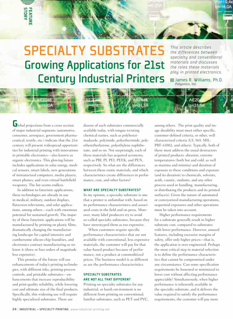
24 | INDUSTRIAL + SPECIALTY PRINTING www.industrial-printing.net
FEATURE STORY
Global projections from a cross section of major industrial segments (automotive, consumer, aerospace, government pharma-ceutical, textile, etc.) indicate that the 21st century will present widespread opportuni-ties for industrial printing with innovations in printable electronics—also known as organic electronics. This glowing future includes applications in solar energy, medi-cal sensors, smart labels, new generations of miniaturized computers, media players, smart phones, and even virtual battle eld weaponry. The list seems endless.
In addition to futuristic applications, these technologies are already in use in medical, military, outdoor displays, atscreen televisions, and solar applica-tions, among others—each with enormous potential for sustained growth. The major-ity of these futuristic applications will be manufactured by printing on plastic lms, dramatically changing the manufactur-ing landscape for capital intensive and cumbersome silicon-chip foundries, and electronics contract manufacturing as we know it (three or four orders of magnitude less expensive).
This promise of the future will use enhancements of today’s printing technolo-gies, with different inks, printing-process controls, and printable substrates—en-hancements that increase reproducibility and print-quality reliability, while lowering cost and ultimate size of the nal products. Speci cally, this widening use will require highly specialized substrates. There are
dozens of such substrates commercially available today, with tongue-twisting chemical names, such as polybenzi-madazole, polyimide, polyetherimide, poly-etheretherketone, polyethylene naphthe-nate, and so on. Not surprisingly, each of these materials has acquired acronyms, such as PBI, PI, PEI, PEEK, and PEN, respectively. So what are the differences between these exotic materials, and which characteristics create differences in perfor-mance, cost, and other factors?
WHAT ARE SPECIALTY SUBSTRATES?In my opinion, a specialty substrate is one that a printer is unfamiliar with, based on its performance characteristics and associ-ated costs in the eld and on press. More-over, many label producers try to avoid so-called specialty substrates, because they have stereotyped them as too expensive.
When customers require speci c performance characteristics that are not available with conventional, less expensive materials, the customer will pay for that value-based product because of perfor-mance, not a product at commoditized prices. The business model is as different as are the performance characteristics.
SPECIALTY SUBSTRATES ARE NOT ALL THAT DIFFERENT Printing on specialty substrates for any industrial, or harsh environment is no different from printing on conventional, familiar substrates, such as PET and PVC,
among others. The print quality and im-age durability must meet either speci c, customer-de ned criteria, or other, well characterized criteria (UL 969, MIL-PRF-61002, and others). Typically, both of these must address the usual destructors of printed products: abrasion, extreme temperatures (both hot and cold, as well as maxima and minima) and duration of exposure to these conditions and exposure (and its duration) to chemicals, solvents, acids, caustic, oxidants, and any other process used in handling, manufacturing, or distributing the products and its printed surface(s). Given the nature of automated or conveyorized manufacturing operations, sequential exposures and other operations must be taken into account.
Higher performance requirements for a substrate generally result in higher substrate cost, compared to substrates with lower performance. However, unused features, including excessive margins of safety, offer only higher prices—that is, the application is over-engineered. Perhaps the most critical step in material selection is to de ne the performance characteris-tics that cannot be compromised under any circumstance. Can some speci cation requirements be loosened or minimized to lower cost without affecting performance appreciably? Simultaneously, when higher performance is inherently available in the specialty substrate, and it delivers the value required to satisfy the performance requirements, the customer will pay more
SPECIALTY SUBSTRATESGrowing Applications for 21st
Century Industrial Printers
This article describes the differences between specialty and conventional materials and discusses the roles these materials play in printed electronics.
James R. Williams, Ph.D.Polyonics, Inc.
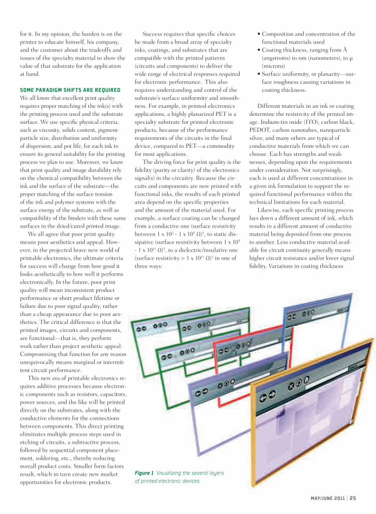
for it. In my opinion, the burden is on the printer to educate himself, his company, and the customer about the tradeoffs and issues of the specialty material to show the value of that substrate for the application at hand.
Some paradigm ShiftS are requiredWe all know that excellent print quality requires proper matching of the ink(s) with the printing process used and the substrate surface. We use specific physical criteria, such as viscosity, solids content, pigment-particle size, distribution and uniformity of dispersion, and pot life, for each ink to ensure its general suitability for the printing process we plan to use. Moreover, we know that print quality and image durability rely on the chemical compatibility between the ink and the surface of the substrate—the proper matching of the surface tension of the ink and polymer systems with the surface energy of the substrate, as well as compatibility of the binders with these same surfaces in the dried/cured printed image.
We all agree that poor print quality means poor aesthetics and appeal. How-ever, in the projected brave new world of printable electronics, the ultimate criteria for success will change from how good it looks aesthetically to how well it performs electronically. In the future, poor print quality will mean inconsistent product performance or short product lifetime or failure due to poor signal quality, rather than a cheap appearance due to poor aes-thetics. The critical difference is that the printed images, circuits and components, are functional—that is, they perform work rather than project aesthetic appeal. Compromising that function for any reason unequivocally means marginal or intermit-tent circuit performance.
This new era of printable electronics re-quires additive processes because electron-ic components such as resistors, capacitors, power sources, and the like will be printed directly on the substrates, along with the conductive elements for the connections between components. This direct printing eliminates multiple process steps used in etching of circuits, a subtractive process, followed by sequential component place-ment, soldering, etc., thereby reducing overall product costs. Smaller form factors result, which in turn create new market opportunities for electronic products.
Success requires that specific choices be made from a broad array of specialty inks, coatings, and substrates that are compatible with the printed patterns (circuits and components) to deliver the wide range of electrical responses required for electronic performance. This also requires understanding and control of the substrate’s surface uniformity and smooth-ness. For example, in printed-electronics applications, a highly planarized PET is a specialty substrate for printed electronic products, because of the performance requirements of the circuits in the final device, compared to PET—a commodity for most applications.
The driving force for print quality is the fidelity (purity or clarity) of the electronics signal(s) in the circuitry. Because the cir-cuits and components are now printed with functional inks, the results of each printed area depend on the specific properties and the amount of the material used. For example, a surface coating can be changed from a conductive one (surface resistivity between 1 x 10² - 1 x 10⁵ Ω)3, to static dis-sipative (surface resistivity between 1 x 10⁵ - 1 x 10¹¹ Ω)3, to a dielectric/insulative one (surface resistivity > 1 x 10¹¹ Ω)3 in one of three ways:
• Composition and concentration of the functional materials used
• Coating thickness, ranging from Å (angstroms) to nm (nanometers), to µ (microns)
• Surface uniformity, or planarity—sur-face roughness causing variations in coating thickness.
Different materials in an ink or coating determine the resistivity of the printed im-age. Indium-tin oxide (ITO), carbon black, PEDOT, carbon nanotubes, nanoparticle silver, and many others are typical of conductive materials from which we can choose. Each has strengths and weak-nesses, depending upon the requirements under consideration. Not surprisingly, each is used at different concentrations in a given ink formulation to support the re-quired functional performance within the technical limitations for each material.
Likewise, each specific printing process lays down a different amount of ink, which results in a different amount of conductive material being deposited from one process to another. Less conductive material avail-able for circuit continuity generally means higher circuit resistance and/or lower signal fidelity. Variations in coating thickness
Figure 1 Visualizing the several layers of printed electronic devices
James R. Williams, Ph.D.Polyonics, Inc.
may/june 2011 | 25
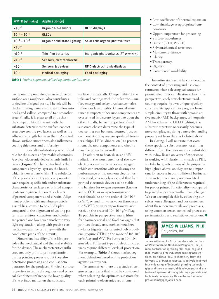
26 | IndustrIal + specIalty prIntIng www.industrial-printing.net
from point to point along a circuit, due to surface-area roughness, also contributes to decline of signal purity. The ink will be thicker in rough areas as it tries to flow into peaks and valleys, compared to a smoother area. Finally, it is clear to all of us that the compatibility of the ink with the substrate determines the surface-contact area between the two layers, as well as the adhesion strength between them. As noted above, surface smoothness also influences coating thickness and uniformity.
Specialty substrates play a critical role for the success of printable electronics. A typical electronic device is truly built in layers (Figure 1). The printer builds the components layer by layer on the board, which is now a plastic film. The subtleties of the printed circuitry and components each require specific ink and/or substrate characteristics, as layers of printed compo-nents are registered upon other layers of printed components and circuits. Align-ment problems with membrane-switch assemblies promise to be child’s play compared to the alignment of coating pat-terns as resistors, capacitors, and diodes are printed one layer over another in very tight registration, along with precise con-nection—again, by printing—with the conductive paths of the circuits.
Dimensional stability of the film pro-vides the mechanical and thermal stability for the device. These characteristics influ-ence not only print-to-print registration during printing processes, but they also determine processing and end-use tem-peratures for the products. Physical surface properties in terms of roughness and physi-cal cleanliness influence the layer quality of the printed matter on the substrate
surface dramatically. Compatibility of the inks and coatings with the substrate—sur-face energy and solvent resistance—also influences layer quality. Chemical resis-tance is important because components are overprinted in discrete layers one upon the other. Finally, barrier properties of each substrate chosen determine the type of device that can be manufactured. Just as components today are encapsulated (resis-tors, chips, LEDs, diodes, etc.) to protect them, the new components and circuits must be protected as well.
In addition to heat, dust, and UV radiation, the worst enemies of the new electronics are water vapor and oxygen, which can interfere with or destroy the performance of the new-era electronics. In general, it is widely accepted that for printed electronic devices to be viable, the barriers for oxygen exposure (known as the OTR, or oxygen transmission rate) should be on the order of 10-3-10-5 cc/m2/day, and for water vapor (known as the WVTR or water vapor transmission rate), on the order of 10-3-10-6 g/m2/day. To put this in perspective, many films forpharmaceutical and food packages that printers already use, such as metalized mylar or high-tensity-oriented polypropyl-ene, require OTRs in the range of 100-10-2 cc/m/day and WVTRs between 10-1-10-3 g/m2/day. Different types of electronic de-vices require different levels of protection. For example, Table 1 shows market-seg-ment definition based on the protection against water vapor.
To summarize, there are a stack of en-gineering criteria that must be considered when selecting the optimum substrate for each printable-electronics requirement:
WVTR (g/m2/day) Application(s)
<10-6 Organic bio-sensors OLED displays
10-5 – 10-6 OLEDs
10-4 – 10-5 Organic solid state lighting Solar cells organic photovoltaics
<10-4
<10-3 Thin-film batteries Inorganic photovoltaics (2nd generation)
<10-2 Sensors, electrophoretic
<10-1 Sensors & devices RFID electrochromic displays
10-1 Medical packaging Food packaging
Table 1 Market segments defined by barrier performance
• Low coefficient of thermal expansion• Low shrinkage at appropriate tem-
peratures• Upper temperature for processing• Surface smoothness• Barrier (OTR, WVTR)• Solvent/chemical resistance• Moisture resistance• Clarity• Transparency• Rigidity• Commercial availability
The entire stack must be considered in the context of processing and use envi-ronments when selecting substrates for printed-electronics applications. From this perspective, each new electronic prod-uct may require its own unique specialty substrate. As applications progress from simple circuitry to those with organic ac-tive matrix (AM) backplanes, to inorganic AM backplanes, to OLED lighting, the substrate structure necessarily becomes more complex, requiring a more demanding property set from the stacks listed above.
In closing, I will reiterate that even these specialty substrates are not all that different from the ones we are comfortable with today. Based on years of experience in working with plastic films, such as PET, we take for granted many of the properties highlighted above; or, they are not impor-tant for success in our traditional business. It is our technical and process-related understanding of the differences required for proper printed functionality—compared to printed appearance—that must change. We can accomplish this by educating our-selves, our colleagues, and our customers about these new materials and processes, using common sense, controlled process ex-perimentation, and realistic expectations.
James Williams, Ph.D, is founder and chairman of Westmoreland, NH-based Polyonics, Inc., a manufacturer of specialty film, tape, tag, and label materials for industrial printing applica-tions. He holds a Ph.D. in chemistry from the University of Massachusetts, is actively involved in a wide range of industrial printing technolo-gies and their commercial development, and is a featured speaker at many printing symposia and technical conferences. He can be contacted at [email protected].
James WIllIams, ph.dPolyonics, Inc.

ANNOUNCING...A new Website that speaks to the unique needs of industrial printing facilities
Late-breaking news Features Editorials New products Calendar Classifi eds Free posted user forums
www.linkedin.com/groups?gid=2658424
www.twitter.com/iSPmag
www.facebook.com/iSPmag
News & Trends Products Message Boards
INDUSTRY UPDATE PRODUCTS & TECHNOLOGY
TECHNIQUES, TIPS & APPLICATIONS
Top Stories • Printing Photovoltaics Screen printing photovoltaic cells
is the most reliable method and fastest growing application in industrial printing.
• Automating Your Pad-Printing Operation
Automation is an important part of effi cient, consistent pad printing. Find out about some of the options designed to enhance speed and precision for industrial applications.
• Membrane Switch: Screen Printing 101
The membrane-switch market has experienced dramatic growth and soared to an unprecedented level.
• Industry InsiderThe Importance of Printed Electronics to P&G
Textured Polyester Film >>
Conductive inks Decals / nameplates Finishing and QC Hot stamping In-mold decorating Inkjet printing
username password Log in
March/april 2010
www.industrial-printing.net
printingphotovoltaicsP. 22
SubscribeToday
Printing equipment used in manufacturing
Advertising OpportunitiesContactSteve Duccilli800.925.1110 [email protected]
28 | INDUSTRIAL + SPECIALTY PRINTING www.industrial-printing.net
FEATURE STORY
Roll-to-Roll Printing in Electronics Applications
The printed-electronics eld is garnering attention from entrepreneurs, investors, and researchers around the world. This eld of industry is multidisciplinary; as such, combined knowledge in machinery, materials, manufacturing process, and business is necessary to deliver the right product to the right market.
As the name suggests, printed electron-ics involves using a printing process in the manufacture of electronic devices and products. These processes include gravure, offset, exography, inkjet, screen printing, and many more. Some technical challenges arise from the use of printing in producing electronics. We discuss them further on in this article.
At this stage of technological develop-ment, printing on either rigid or exible substrates is considered a supplement to or replacement for traditional electronic-device-manufacturing processes. Table 1 summarizes the comparison between printed media—newspapers and maga-zines, for example—and printed electron-ics. The difference stems from the fact
Deokkyun Yoon and Dong-Soo KimKorea Institute of Machinery and Materials
that printed media are used to convey information for people to process using their eyes, while printed electronic devices require machines to process electronic in-formation; the level of required resolution and functionality make the difference.
Some of the widely used functional materials for printed electronics include nano/micro-size metal particles, semicon-ductive polymers, and dielectric materials. Due to the available and required readout resolution, feature sizes smaller than 20 μm need to be printed. Layer thick-ness and registration accuracy of printed products are closely related to quality control of electronic devices, and ink materials require a high level of quality. Overall, printing tolerance is much tighter in printed electronics.
ROLL-TO-ROLL PRINTINGRoll-to-roll printing is considered the holy grail of manufacturing processes for production of exible and large-area electronics. Substrate materials used in roll-to-roll printing are typically paper and
is article describes the current state of roll-fed electronics printing and discusses what we may expect to see in the near future.
plastic lms. Metal foil is also widely used in solar-cell and energy-storage applica-tions. Plastic lms such as PET, PEN, and PC are commonly used for their low cost; however, the use of plastic lm has involves some technical challenges that must be addressed.
Electronic devices, such as TFTs, solar cells, supercapacitors, thin- lm batteries, RFID circuits and OLEDs, are produced continuously by various additive processes, such as exography, gravure, offset, inkjet, and slot-die coating, in the order of square meters per second. This type of manufac-turing process increases productivity by orders of magnitude when compared to the processes used in semiconductor fabrica-tion, such as lithography for silicon wafers.
Gravure, offset, and exography are most commonly used in roll-to-roll printed electronics. Figure 1 summarizes and compares some of the manufacturing processes used for printed electronics in throughput and feature-size areas. You will see that gravure, offset, and exography have an advantage in high-speed processing
MAY/JUNE 2011 | 29
and throughput while achieving medium resolution. Researchers around the world are actively seeking ways to achieve smaller feature size while maintaining high pro-ductivity.
PRINTING PROCESSESLet’s discuss the aforementioned three printing processes in greater detail. Gra-vure, exography, and offset printing were developed in the 19th century. Originally used in printed media, these processes are now used to print functional inks on ex-ible substrates.
In gravure printing, patterns to be transferred to the substrate are engraved on a cylinder (Figure 2). Engraving methods include chemical etching, laser machin-ing, and direct mechanical machining. The entire patterned cylinder—also called the plate cylinder—is covered with ink (viscos-ity 50-200 cP). Then, the excess ink is doctored off, leaving ink in the cup-shaped engraved pattern. The plate cylinder is brought in contact with the impression cylinder to transfer what is in the ink cup to the substrate. Controlling impression pressure changes the surface energy, giving room for ink transfer control.
In exography, only the raised area in the pattern cylinder is inked, and the pat-tern is transferred to the substrate (Figure 3). A soft, raised pattern is often used instead of a hard pattern, and due to this common usage, the achievable feature size tends to be bigger than gravure. Flexo ink is similar in viscosity to formulations used in gravure.
Offset is slightly different from the two methods shown above. First, it requires an ink with a much higher viscosity (20,000-100,000 cP). Second, it uses a blanket cyl-inder that bridges the plate cylinder and the substrate. The pattern is transferred to the blanket, typically made of rubber, and then the transferred pattern is re-transferred to the substrate. The former process is called off and the latter is called set.
One of the advantages of the offset method is that it can use low impres-sion pressure. Where layers of functional materials are deposited on top of each other, high impression pressure commonly seen in the gravure method may damage other functional layers underneath. On the other hand, the print quality depends on the nature of the blanket rubber. The
Printed Media Printed ElectronicsInk requirement Color (visuals) Electronic performance
(conductivity, semiconductivity, dielectric, etc.)
Ink material Color pigment Functional materialResolution > 20 μm < 20 μmLayer thickness ~ 1 μm 0.1 - 0.3 μmRegistration ± 50 μm ± 1 – 10 μmInk homogeneity Somewhat important Very importantInk formulation Cost driven Function drivenInk chemistry purity Somewhat important Very importantInk transfer Small issue Big issue
Rotary screen
Laser ablation
R2R photolitho
Ink-jet
Flat screen
Off set Gravure
Flexo
ro
roug
hput
(m2/s
)
Low
(<0.
01)
Med
ium
(0
.01-
1)Hi
gh (>
1)
100
1
10-2
10-4
Minimum feature size (µm)
High Resolution (<10 µm)
Medium Resolution (10-50 µm)
Low Resolution (>50 µm)
1 10 100 500
Table 1 Printed media vs. printed electronics
Figure 1 roughput vs. feature size for typical production processes
Ink
Gravure cylinderBlade
Impression cylinder
Image elements are equally spaced but variable in depth and area
Figure 2 Gravure printing
30 | INDUSTRIAL + SPECIALTY PRINTING www.industrial-printing.net
blanket rubber absorbs solvent and gets swollen over time, which leads to a change in absorption rate. Solving this issue is one of the most important technical challenges in system reliability.
The method of delivering a pattern to the blanket cylinder is up to the user. Pat-tern transfer in offset printing relies on the properties of two different inking solutions (Figure 4). Because the nal product in printed electronics requires not only the visuals, but also the functionality, this traditional method used in printed media is not readily applicable. To addressing this issue, a gravure plate cylinder can be used to transfer a pattern to the blanket cylinder in lieu of direct transfer to the substrate.
This speci c method is called gravure-off-set. Recent research results suggest that it is possible to produce feature sizes smaller than 10 μm in a continuous roll-to-roll fashion using this gravure-offset method.
WEB-TRANSPORT CONTROLPrecise web-transport control is necessary to guarantee sound functionality of the n-ished product. Having uniform tension on the substrate web throughout the process is important. Abrupt changes compromise the stability of deposited materials. The mate-rial web expands in response to force load-ing, and change in strain may cause cracks, short circuiting, and delamination of layers. Tension disturbance, which is caused by either an outside source or equipment design itself, should be minimized and affected materials should be rejected upon detection.
Another important aspect of web-trans-port control is velocity control. Precise syn-chronization of various cylinders in printing equipment is needed to ensure the printing quality and reliability of functional materi-als. Under precise angular velocity control, axles on feeder, plate cylinders, blanket cylinders, and impression cylinders are all in perfect harmony to achieve ne printing lines and uniform print thickness. Take this simple calculation for example: 10 arc-sec (that is 1/360 of a degree, and this state of precision is expensive to achieve) difference on a shaft with 300-mm-radius roll equates to a difference of 15 µm, which in some printed-electronics applications crosses the line between overall success and failure.
DRYING AND CURING TECHNOLOGYPrinted ink is typically dried and cured us-ing hot air and/or ultraviolet (UV) rays. Hot air blown toward the substrate is the most commonly used implementation of the drying system; the air temperature is set, and a blower sends the hot air toward the substrate where needed. These methods mainly have two shortcomings: long curing times and thermal strain on exible sub-strates. These shortcomings are somewhat interrelated.
Because most printed-electronics devices are made on plastic lm, high temperature drying and curing are not easy to implement. The glass-transition temperature for plastics is as low as 80°C. Higher curing temperatures are possible when glass or metal substrates are used, but these materials are not common in roll-to-roll applications; glass is rigid, and metal foil is expensive. Because drying and curing are done at relatively low temperatures, it takes several minutes or more—in some cases, hours—of drying and curing time for proper performance of functional materials. When everything is processed continu-ously inline, this means a very long dryer. Increasing the curing temperature is not a feasible option because the substrate’s stiff-ness decreases as temperature increases and the substrate itself starts melting when its melting point is exceeded.
Another shortcoming discussed above is the thermal strain on exible substrates. Substrate material length can be extended up to a couple of percentage points under thermal stress inside the hot-air dryer.
Elastic printing plate with inked image elements
Cells of the anilox roller ink-fi lled
Elastic printing platePrinting substrate
Hard impression cylinder
Ink supply
Anilox roller
Figure 3 e fl exographic printing process
Inking system
Plate cylinder
Impression cylinder
Blanket cylinder
Dampening system
Figure 4 e off set printing process
Inking
Printing plate
Oleophilic ink-accepting area
Hydrophilic ink-repellent area
Residual ink layer
Dampening

may/june 2011 | 31
Thermal expansion complicates the ten-sion and velocity control algorithm. Thor-ough knowledge of how they influence each other is needed to address this issue. Knowing how much the substrate’s length would increase is essential in maintaining the desired web tension and shaft synchro-nization. Thermal strain coupled with a long hot-air dryer makes registration control a difficult problem to solve.
Some novel methods are being pro-posed and studied to address problems associated with drying and curing. They include laser curing and pulsed, high-intensity light curing. The commonality between the two is that they both use high-energy discharge and selective cur-ing of ink material. In laser curing, the wavelength of the laser is chosen strate-gically to target solvent and functional materials to deliver the right amount of energy, which shortens processing time and reduces the possibility of substrate damage. Similarly, the pulsed, high-inten-sity light source can be discharged with a large amount of energy—in the order of tens of MJ—during a short period of time (microseconds or milliseconds) to evaporate the solvents instantly and cure the functional materials. Because of the very short process time, there is no time for heat transfer to take place, leaving the substrate undamaged from high heat energy. Some of these types of equipment are available on the market today for selec-tive ink materials.
RegistRation accuRacyRegistration accuracy, the hottest research topic of late in roll-to-roll printing, is the ability to print multiple layers on top of each other precisely as requested by the device designer. Registration technologies were devel-oped in printed media to apply four-color inksets (CMYK) ac-curately to create a vast array of colors. Printed electronics involves the deposition of layers of different functional materials. For example,
several layers of functional materials need to be printed to create an RFID tag, and desired feature size approaches 20-30 μm.
Registration accuracy is more important in printed electronics than it is in printed media because human eyes can only detect defects that are approximately 50 µm or larger. Printing equipment designed for media product was developed to meet the requirements of the human eye. This level of accuracy cannot be applied to many printed-electronics applications, such as printed TFTs for display backplanes, where electric circuitry must be printed with registration tighter than 10 μm.
Many printing presses now implement optical measurement systems that use high-speed, high-resolution cameras (Figure 5). The cameras are used to measure the regis-tration accuracy in the printed product, and this information is fed back to the control system. The control system modulates the angular velocity of successive printing cylinders to compensate for errors. The key to controlling registration accuracy is thorough knowledge of how web tension, transport velocity, and registration accuracy are interconnected; these three measurable attributes are joined together. You must make strategic decisions about how to con-trol these attributes in advance and during the design stage.
mateRialsThe printed electronics we know to-day—and hope for tomorrow—wouldn’t be
possible without functional, roll-to-roll ma-terials. Having the right material with right functional properties—mobility, dielectric constant, conductivity, and more—is essential to produce electronic devices that operate as product designers intend. Note that the printed-electronics business revolves around printed products that have functional performance and visual require-ments to meet.
Functional materials must be durable, repeatable, and—most importantly—print-able. Materials suppliers are working hard to deliver mass-produced substrates for the printed-electronics industry. Last, but not the least, printable materials must dry or cure quickly. Considering all these require-ments, many materials are still in the development stage, and more work must be done in functional-materials research and development.
FutuRe outlookIt has been about a decade since the term printed electronics gained profound mean-ing in the business of electronics manufac-turing. Researchers and companies around the world are dedicating their resources to investigate and develop solutions to achieve the key technical attributes in the web control, drying and curing technology, and printable materials. Starting from rudimen-tary product groups that require low-resolu-tion printing and simple structures, printed electronics—especially roll-to-roll applica-tions—will be in our daily lives soon.
Figure 5 High-resolution cameras are central to the optical measurement systems used to ensure optimum print quality and functionality in printed-electronics applications.
Deokkyun Yoon is a researcher at Korea Institute of Machinery and Materials. His research interest includes machine design and control in printing applications. He holds B.S. and M.S. degrees in mechanical engineering from the University of Michigan.
Deokkyun yoonKorea Institute of Machinery and Materials
Dong-Soo Kim is the vice president of Korea Institute of Machinery and Materials and the principal investigator of numerous government-funded research projects in printed electronics. He holds B.S., M.S., and Ph.D. degrees in me-chanical engineering from Yeongnam University.
Dong-soo kimKorea Institute of Machinery and Materials
32 | IndustrIal + specIalty prIntIng www.industrial-printing.net
prIntIng M
etHOds
Functional printing: Maskless deposition of sensorsThere are many application areas for sensors, and market studies forecast future growth in the sensor market within the next few years. In addition to conventional sensors made by using microsys-tems technology, functional printing allows for the direct deposi-tion of sensors and other functional structures—conductive paths on different planar and non-planar surfaces and components by means of maskless printing technologies, for example.
FunctIOnal prIntIngFunctional printing (Figure 1) starts with a structural layout that usually comes in a CAD (computer-aided design) file adapted to the desired function, process, and used surface. It follows the material selection and development step. Typical materials for functional printing are nanoscale suspensions or so-called functional inks. These inks consist of nanoparticles dispersed in a fluid. Additionally, stabilizing agents are used to avoid agglom-eration and particle sedimentation. Here, a wide range of differ-ent materials can be used, such as commercially available metal and ceramic inks. Polymer inks are also available, and different metal-alloy suspensions can be produced by using sputtering and other processes.
The next steps include maskless printing and, finally, thermal activation of the printed structures for densification. Typical print-ing technologies include high-resolution processes such as inkjet and Aerosol Jet, the latter of which was developed by Optomec Inc. to handle suspensions with a viscosity range from 0.7-1000 mPa∙s and a particle size up to 1000 nm for metals. The so-called atomizer produces an aerosol from the suspension, which is car-
Marcus Maiwald, Christian Werner, and Volker ZöllmerFraunhofer Institute for Manufacturing Technology and Advanced Materials Research
ried to the printhead. A sheath gas (nitrogen) is used inside the printhead to focus the aerosol beam and prevent nozzle clogging. The aerosol droplets have a diameter of 1-5 µm, which corre-sponds to volumes calculated in femtoliters. The use of sheath gas and the focused aerosol beam enable Aerosol Jet to print on non-planar surfaces.
There are different solutions for the thermal activation that depend on the printed material and the surface or component. Polymer inks typically are cured using a furnace or UV curing. Metal inks are mostly sintered using a furnace or a laser. The final structure is characterized in terms of physical, electrical, and other properties.
FunctIOnal prInted sensOrs and straIn gaugesNon-destructive testing is very important—especially with aerospace and automotive products. Here, functional printing offers the possibility of depositing metal strain gauges directly on surfaces and components for continuous measurements. The piezoresistive effect enables strain gauges to measure stress and strain. A change in length of the strain gauge is proportional to a change in electrical resistance. Commercially available strain gauges are mostly fabricated on foil substrates and consist of a metal-alloy meander. Metal-alloy materials are used because of the small temperature coefficient of resistance, which means that temperature will not influence the strain signal.
Foil strain gauges are glued onto substrates or components. Functional, printed strain gauges have the advantages that the strain gauge is placed automatically via the printing process, and
LayoutMaterial Development/Ink formulation
Printing process Thermal activation Characterization
Figure 1 The functional printing process steps
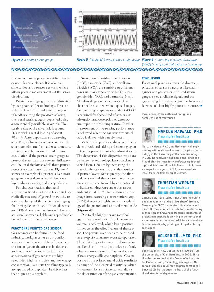
may/june 2011 | 33
the sensor can be placed on either planar or non-planar surfaces. It is also pos-sible to deposit a sensor network, which allows precise measurements of the strain distribution.
Printed strain gauges can be fabricated by using Aerosol Jet technology. First, an isolation layer is printed using a polymer ink. After curing the polymer isolation, the metal strain gauge is deposited using a commercially available silver ink. The particle size of the silver ink is around 20 nm with a metal loading of about 50 wt %. After deposition and sintering at 350°C, diffusion processes connect the silver particles and form a dense structure. At last, the polymer ink is used for en-capsulation of the printed strain gauge to protect the sensor from external influenc-es. The total thickness of all three printed layers is approximately 20 µm. Figure 2 shows an example of a printed silver strain gauge on a metal surface with isolation layer, silver meander, and encapsulation.
For characterization, the metal substrate is fixed in a tensile tester and pe-riodically stressed. Figure 3 shows the re-sistance change of the printed strain gauge for 7675 cycles with 1000-N tensile stress and 500-N compressive stresses. The sen-sor signal shows a reliable and reproducible behavior within the tested range.
Functional printed gas sensor Gas sensors can be found in the food industry, workplaces, or as air-quality sensors in automobiles. Harmful concen-trations of gas in the air can be detected and counteraction initialized. Typical specifications of gas sensors are high selectivity, high sensitivity, and low energy consumption. Gas-sensitive films typically are sputtered or deposited by thick-film techniques on a hotplate.
Several metal oxides, like tin oxide (SnO2), zinc oxide (ZnO), and wolfram trioxide (WO3), are sensitive to different gases such as carbon oxide (CO), nitro-gen dioxide (NO2), and ammonia (NH3). Metal-oxide gas sensors change their electrical resistance when exposed to gas. An operating temperature of about 400°C is required for these kind of sensors, as adsorption and desorption of gases oc-curs rapidly at this temperature. Further improvement of the sensing performance is achieved when the gas-sensitive metal oxide is doped with a noble metal.
Metal-oxide powder is dispersed in eth-ylene glycol, and adding a dispersing agent to the ink prevents particle sedimentation. The deposition of this dispersion was done by Aersol Jet technology. Layer thickness varied from 1-20 µm by increasing the material-deposition rate and the number of printed layers. Subsequently, the ther-mal treatment of the printed metal-oxide structure was performed by conventional radiation-conduction-convection under ambient air at 700°C for 30 minutes. An image from scanning electron microscopy (SEM) shows the highly porous morphol-ogy of the printed and sintered metal oxide (Figure 4).
Due to the highly porous morphol-ogy, an increased ratio of surface area to volume is achieved, which has a positive influence on the effectiveness of the sen-sor. The porous layer needs to be printed on a hotplate to ensure accurate operation. The ability to print areas with dimensions smaller than 1 mm and a thickness of only a few microns allows for the development of new energy-efficient hotplates. Gas ex-posure of the printed metal oxide results in a change of the electrical resistivity, which is measured by a multimeter and allows the determination of the gas concentration.
conclusionFunctional printing allows the direct ap-plication of sensor structures like strain gauges and gas sensors. Printed strain gauges show a reliable signal, and the gas-sensing films show a good performance because of their highly porous structure.
Please consult the authors directly for a complete list of references.
Figure 2 A printed strain gauge Figure 3 The signal from a printed strain gauge Figure 4 A scanning electron microscope (SEM) photo of a printed metal oxide close up
Marcus Maiwald, Ph.D., studied electrical engi-neering with main emphasis micro system tech-nology at the University of Bremen, Germany. In 2006 he received his diploma and joined the Fraunhofer-Institute for Manufacturing Technol-ogy and Advanced Materials Research in Bremen as project manager. In 2010, he received his Ph.D. from the University of Bremen.
marcus maiwald, ph.d.Fraunhofer Institute
Christian Werner studied industrial engineering and management at the University of Bremen, Germany. In 2007, he received his diploma and joined the Fraunhofer Institute for Manufacturing Technology and Advanced Materials Research as project manager. He is working in the functional structures department and with focus on surface functionalization by printing and rapid sintering techniques.
christian wernerFraunhofer Institute
Volker Zöllmer, Ph.D., obtained his degree from the University of Kiel, Germany, in 2002. Since then he has worked at the Fraunhofer Institute for Manufacturing Technology and Applied Ma-terials Research in Bremen as project manager. Since 2003, he has been the head of the func-tional structures department.
Volker Zöllmer, ph.d.Fraunhofer Institute

34 | IndustrIal + specIalty prIntIng www.industrial-printing.net
reduced solar Module shipments predicted for 2011
According to market forecaster Solar-buzz, following a strong growth of 139% in 2010, global solar photovoltaic demand is off to a weak start in 2011. Preliminary esti-mates of Q1 2011 end-market demand in Germany show it
running at less than 50% of its Q1 2010 level. The gradual price reduc-tions seen so far this year have been insufficient in energizing the market. However, in Q2 2011, global demand is still projected to reach 7.4 GW, representing 77% Y/Y growth, according to the latest Solar-buzz report.
Any changes to government PV policies as a consequence of the nuclear disaster that has followed the earthquake and tsunami in Japan are not expected to impact demand until 2012. At the same time, the disaster’s impact on the nine major plants engaged in poly-silicon wafer and cell production in Japan so far appear to be minimal.
Craig Stevens, president of Solarbuzz, says, “2011 will be a chal-lenging year for the industry as it manages a slowdown in the market. Europe will not be the growth engine it has been in recent years, and manufacturers will need to access new markets or be exposed to the risk of rising inventories or production cuts during a period of falling prices.”
Industry neWs
Market m
ovements and association updates
Polysilicon in China in Tight SupplyChina imported 5,521 tons of polysilicon in January, representing a year-on-year rise of 74.8%, according to the latest stats released by the General Administration of Customs. The figure is 40% above the 2010 average monthly import, which was approximately 3,958 tons, providing evidence that the material is in tight supply across the country.
The domestic supply shortages are attributable to a production halt as a result of rou-tine year-end audits performed by major polysilicon makers in China before the Chinese Spring Festival break. Polysilicon imports in February were high as well.
Tight supplies of polysilicon, which is used in the manufacture of solar PV modules, is experiencing rapid price hikes. The spot price for polysilicon has reached $114 per kilogram early in March—an increase of nearly 100% from the end of last year.
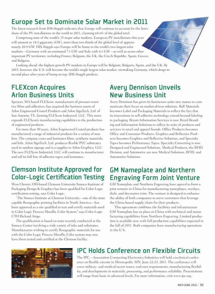
may/june 2011 | 35
Europe Set to Dominate Solar Market in 2011The latest research from IHS iSuppli indicates that Europe will continue to account for the lion’s share of the PV installations in the world in 2011, claiming 68.6% of the global total.
Comprising nine of the world’s 15 major solar markets, European PV installations this year will amount to 14.3 gigawatts (GW), more than two-thirds of the global level of approxi-mately 20.9 GW. HIS iSuppli says Europe will be home to the world’s two largest solar markets—Germany with an estimated 7.1 GW and Italy with 4.1 GW—as well as seven other important PV territories, including France, Belgium, the UK, the Czech Republic, Spain, Greece, and Bulgaria.
Looking ahead, the highest growth PV markets in Europe will be Belgium, Bulgaria, Spain, and the UK. By 2015, however, the U.S. will become the world’s single largest solar market, overtaking Germany, which drops to second place after years of being on top, IHS iSuppli predicts.
FLEXcon Acquires Arlon Business Units Spencer, MA-based FLEXcon, manufacturer of pressure-sensi-tive films and adhesives, has acquired the business assets of Arlon Engineered Coated Products and Arlon SignTech, Ltd. of San Antonio, TX, forming FLEXcon Industrial, LLC. This move expands FLEXcon’s manufacturing capabilities to the production of engineered products.
For more than 50 years, Arlon Engineered Coated products has manufactured a range of industrial products for a variety of mar-kets. The company coats and laminates films, synthetic materials, and foils. Arlon SignTech, Ltd. produces flexible PVC substrates used in outdoor signage and is a supplier to Arlon Graphics, LLC. The new FLEXcon Industrial, LLC will continue to manufacturer and sell its full line of adhesive tapes and laminates.
Clemson Institute Approved for Color-Logic Certification TestingWest Chester, OH-based Clemson University Sonoco Institute of Packaging Design & Graphics has been qualified for Color-Logic certification testing, says Color Logic.
“The Sonoco Institute at Clemson University—one of the most capable flexographic printing facilities in North America—has been approved as a site qualified to test and certify materials used in Color-Logic Process Metallic Color System,” says Color-Logic CTO Richard Ainge.
The qualification is based on tests recently conducted at the Sonoco Center involving a wide variety of inks and substrates. Manufacturers wishing to certify flexographic materials for use with the Color-Logic Process Metallic Color system may now have them tested and certified at the Clemson facility.
Avery Dennison Unveils New Business UnitAvery Dennison has given its businesses units new names to com-municate their focus on market-driven solutions. Roll Materials becomes Label and Packaging Materials to reflect the fact that its innovations in self-adhesive technology extend beyond labeling to packaging. Retain Information Services is now Retail Brand-ing and Information Solutions to reflect its suite of products and services in retail and apparel brands. Office Products becomes Office and Consumer Products. Graphics and Reflective Prod-ucts becomes Graphics and Reflective Solutions, and Specialty Tapes becomes Performance Tapes. Specialty Converting is now Designed and Engineered Solutions. Medical Products, the RFID Division, and Automotive are now Medical Solutions, RFID, and Automotive Solutions.
IPC Holds Conference on Flexible CircuitsThe IPC—Association Connecting Electronics Industries will hold a technical confer-ence on flexible circuits in Minneapolis, MN, June 22-23, 2011. The conference will cover military- and medical-sector issues, end-user requirements, manufacturing flexibil-ity, and developments in materials, processing, and performance reliability. Presentations will range from basic to advanced levels. For more information, visit www.ipc.org.
GM Nameplate and Northern Engraving Form Joint VentureGM Nameplate and Northern Engraving have agreed to form a joint venture in China for manufacturing nameplates, overlays, dials, and decorative trim. The venture is designed to enhance the ability of both companies to serve customers that leverage the China-based supply chain for their products.
This agreement combines the facilities and infrastructure GM Nameplate has in place in China with technical and manu-facturing capabilities from Northern Engraving. Limited produc-tion is available now with full production capabilities expected in the fall of 2011. Both companies have manufacturing operations in the U.S.

36 | INDUSTRIAL + SPECIALTY PRINTING www.industrial-printing.net
Polyera Names Ramachandran CFOPrakash Ramachandran is now the chief nancial of cer of Polyera. Before leading Polyera’s nancial direction, he was CFO of Nordic Windpower, prior to which he served as CFO of start-up Novariant, a company producing machine-control products for mining and farming industries.
Skokie, IL-based Polyera Corp. is a supplier in semiconductor, dielectric, and interfa-cial materials for the printed- and exible-electronics industry. Polyera’s focus has been on developing materials for its portfolio of ActivInk products.
“We’re delighted that Prakash has decided to join us at Polyera,” says CEO Phil Ina-gaki. “He brings a wealth of experience in fundraising, international nance, and team-building in high-tech industries to our organization, and we know he’ll be a tremendous asset as we continue to build our business.”
LPKF Expands HeadquartersHannover, Germany-based LPKF Laser & Electronics AG, a provider of technologies for PCB prototyping, SMT stencils, PCB processing, laser welding, and more, recently invested €5 million into purchasing a neighboring building, giving an additional 32,000 square feet for product development and production. The new building is currently under renovation and is expected to become a part of the company’s existing complex by June 2011. The company says the need for the additional space stems from the high demand for laser technology and notes that it brought on more than 100 new employees—increas-ing the total to 470—in 2011 to meet this rising demand.
UPCOMING EVENTSMAY 24-27 FESPA HAMBURG, GERMANY www.fespa.com
JUNE 14-16 SGIA Printed Electronics & Membrane Switch SymposiumSAN JOSE, CA www.sgia.org
JULY 12-14 SEMICON West IPCSAN FRANCISCO, CA www.ipc.org
SEPTEMBER 22-23International Conference on Flexible and Printed ElectronicsTOKYO, JAPANwww.icfpe2011.org
SEPTEMBER 27-28 RFID Europe IdTechExCAMBRIDGE, UKwww.idtechex.com
Email gail.fl [email protected] US YOUR NEWS!
PREVIEW Here’s w
hat to expect in the July/August issue of iSP.
FEATURE HIGHLIGHTS:• Organic Solar Cells• Printed Batteries/ Power Supplies• Finishing Processes• E-Book Technology• Automative Labels/Decals• Photovoltaic Update
BUSINESS MANAGEMENT: Matching stencil needs for a changing technologyINDUSTRY INSIDER:Underwriters Lab testing for membrane switches and touchscreens.SHOP TOUR:Photo tour of the Cubbinson Company.
An article submitted by Blue Spark Technologies telling you all about their 1.5v printed battery, and the details for this contest will be in
the July/August issue.
What can you use the battery for?
WILL YOU BE DECLARED A VISIONARY INNOVATOR?
PLUS:
DO YOU CONSIDER YOURSELF AN ORIGINAL THINKER?
IT’S COMING THIS SUMMER!
Blue Spark Technologies, NorTech, and the editors of iSP present,
“Visionary Innovator: Find a Use for is Battery Contest.”
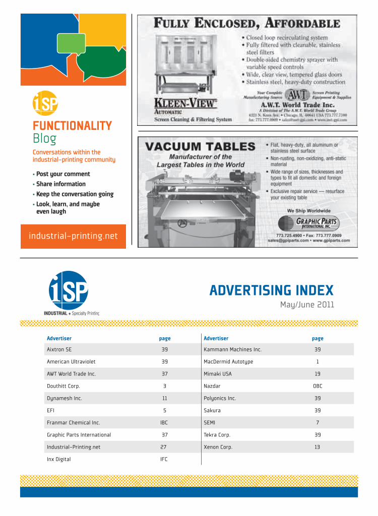
ADVERTISING INDEXMay/June 2011
Advertiser page Advertiser page
Aixtron SE 39 Kammann Machines Inc. 39
American Ultraviolet 39 MacDermid Autotype 1
AWT World Trade Inc. 37 Mimaki USA 19
Douthitt Corp. 3 Nazdar OBC
Dynamesh Inc. 11 Polyonics Inc. 39
EFI 5 Sakura 39
Franmar Chemical Inc. IBC SEMI 7
Graphic Parts International 37 Tekra Corp. 39
Industrial-Printing.net 27 Xenon Corp. 13
Inx Digital IFC
• Post your comment • Share information • Keep the conversation going • Look, learn, and maybe
even laugh
FUNCTIONALITYBlogConversations within the industrial-printing community
industrial-printing.net

38 | IndustrIal + specIalty prIntIng www.industrial-printing.net
Industry InsIder
Beyond Flexible circuits pushing the Boundary for printable electronics
Printable electronics push the outer limits of flexible material standards. For the past two decades, printed electronics have grown and found commercial applications in markets for radio-frequency identifica-tion (RFID), smart labels and displays, sensors, and lighting (OLED). Advance-ments in conductive printable inks, with a little help from nanotechnology, have overcome some of the early consistency problems in conductive additive materi-als. Improvements in printing equipment and processes, including the application of flexo-gravure printing, have made high-speed processing of printable electronics a reality. However, variations in materials and processes for printable electronics cre-ate many opportunities for improvement.
Several of the largest markets for print-able electronics involve being able to pro-cess conductive inks on flexible substrates. Adding some further complications—the substrates are often moving at high speed during ink application. The electronics in-dustry and the graphics-arts industry have met at the crossroads of printed electronics.
IPC standards have provided defini-tion and characterization for traditional flexible electronic circuits for many years. IPC-2223, Sectional Design Standard for Flexible Printed Boards, provides insight into the design requirements for flexible circuits. Drilling down further into the flexible-circuit standards is IPC-4202A, Flexible Base Dielectrics for Use in Flex-ible Printed Circuitry, which defines the flexible bare substrate (dielectric) materi-als. Some of the big issues with flexible substrates are addressed in IPC-4202A including: inspection criteria, dimensional stability, surface finish, strength, tear resistance, etc.
IPC-6013B, Qualification and Perfor-mance Specification for Flexible Printed
dave torpIpc
Boards, provides insights into qualification and performance requirements for flexible printed circuit boards. Some of the require-ments given within IPC-6013B can be directly applied to printable electronics as well. Scratches, surface voids, cover films, adhesion requirements, and accuracy re-quirements are all included in IPC-6013B. Each of the IPC standards for flexible cir-cuits reflects the best practices for design and fabrication using a traditional subtrac-tive process. There are some areas where these standards include additive plating process, as well as adhesive application; however, none of the standards addresses the use of a conductive-ink additive process on which the printable-electronics industry depends.
The printable-electronics market is beginning to mature and experience some of the growing pains that are associated with rapid advancement. For many working in the printable electronic industry, there is a realization that standardization is not too far away. IPC has taken the first steps toward standardization by sponsoring con-ferences on printable electronics. Although no formal standards development has taken place yet, eventually the materials and pro-cesses that reflect best practices within cer-tain segments of the printable-electronics industry will definitely be included in IPC’s future standards-development activities.
Those who have participated on IPC standards-development committees under-stand the power of standards development. IPC connects thousands of subject-matter experts on a global basis. The amount of knowledge that is shared among users, sup-pliers, academia, and laboratories within the electronics community is phenomenal. Problems that seem to be insurmountable to one company are within the core com-petency of another participating company.
IPC standards committees are open to all who want to contribute. There is no fee required to participate on IPC standards-development committees. IPC policies require open and balanced participation on standards-development committees. The output of IPC standards-development committees results in some of the best standards in the world for electronics and the electronics-assembly industry.
The standards-development opportu-nity that exists for printable electronics is in defining the materials and processes for high-performance applications. The uniformity of materials, combined with the process requirements, makes for some great opportunities to develop standards. Development of test methods required to define critical parameters in a reproduc-ible and repeatable way is one of IPC’s core competencies. If you are interested in joining a standards-development group for printable electronics, please contact Dave Torp, vice president standards and technol-ogy, at [email protected].
The next conference on flexible circuits sponsored by IPC will be in Minneapolis, MN, June 22-23, 2011. For more informa-tion, visit www.ipc.org.
David Torp is the VP of standards and technol-ogy for IPC—Association Connecting Electronics Industries, Bannockburn, IL. He has held that position since 2007. Prior to joining IPC, he was a senior staff engineer at Plexus. He also served as VP of marketing and business development at Kester and held various engineering positions at Rockwell Collins as well as Underwriters Laboratories. He has a B.S. degree in Chemical Engineering from Iowa State University.
dave torpIPC
PRODUCT SPOTLGHTA Paid Advertising service to iSP magazine.

40 | IndustrIal + specIalty prIntIng www.industrial-printing.net
shop tour
Screen printing for overlays and circuits
Digital printing for overlays and circuits
Die cutting
Laser cutting for quick-turn samples and prototypes
printeclocatIon Waltham, MA (headquarters in New Taipei City, Taiwan)other Info Printec is a global membrane-switch-manufacturing and technology firm that offers services for high-volume, low-volume, and prototype projects. The company uses a variety of printing, curing, and post-production finishing equipment as part of the manufacturing process. The company’s product line includes membrane switches, flex circuits, touchscreens, integrated touchscreens and LCDs, in-mold-decorated components, overlays and labels, keypads and support panels, and enclosures. Printec is a suppler to a range of markets, including medical, military, aerospace, homeland security, alternative energy, electronics, automotive, and more. For more information, visit www.printec-usa.com.
1 Assembly ranges from simple keypads to more complicated, full-body applications.
QC assesses all products in the assem- bly process.
Printec uses three Class 10,000 cleanrooms.
234
5
6
7
2
1
3
4 5
6
7