Industrial Automation, TI Industrial Packaging · Industrial Automation TI Industrial Packaging...
20
Industrial Automation TI Industrial Packaging Application Report Literature Number: SLDA019 November 2013 – Revised January 2014
Transcript of Industrial Automation, TI Industrial Packaging · Industrial Automation TI Industrial Packaging...

Industrial AutomationTI Industrial Packaging
Application Report
Literature Number: SLDA019November 2013–Revised January 2014

Application ReportSLDA019–November 2013–Revised January 2014
Industrial AutomationTI Industrial Packaging
ABSTRACTAt Texas Instruments, semiconductor packaging is an integral part of the design process and strategicdifferentiator for our Industrial products. TI’s innovative packaging technologies are designed to easilysolve our customers’ most challenging industrial needs by delivering advances in miniaturization,integration, high reliability, high performance, and low power. TI offers a broad Industrial packagingportfolio, built upon decades of packaging expertise developed from supporting thousands of diversifiedpackaging configurations and technologies. Ranging from traditional to the most advanced embeddedsilicon technologies and more, TI is committed to delivering packaging technologies that advance ourproducts today while anticipating our customers’ needs in the future.
Within TI’s broad Industrial packaging portfolio variousform factors are offered to accommodate the everchanging needs of our customers. Ranging fromtraditional monolithic silicon packaging solutions to themost advanced embedded multi-silicon technologiesand more, TI is committed to delivering robustpackaging technologies that fulfill our customers’needs today while anticipating new packaging needsfor the future.
This document offers a variety of subjects such as aconsolidated summary of the packaging familiescategorized by pin count density and form factor, TI’sdefinition of Green and ROHS compliance, Illustrationwith explanation of TI’s moisture sensitivity label,Various figures of merit such as thermal performancemetrics, and a tabulated listing of packages withvarious descriptors to quickly help our customersidentify their package of interest.TI’s diverse Industrial Product Portfolio Includes
2 Industrial Automation TI Industrial Packaging SLDA019–November 2013–Revised January 2014Submit Documentation Feedback
Copyright © 2013–2014, Texas Instruments Incorporated

QFP QFN/SON DIP
Pa
ck
ag
e T
yp
e
Encapsulant Partially Removed For Illustration
Proposes
Encapsulant Partially Removed For Illustration Proposes Encapsulant Partially Removed For Illustration Proposes
Be
ne
fits
Leaded high Pin Count
configurations with efficient
Thermal Path
Space saving from higher Area Ratio
configuration
Industry package outlines results in a large
portfolio of devices available
SOT TSSOP TO
Pa
ck
ag
e T
yp
e
Encapsulant Removed From package base side for
Illustration Proposes Encapsulant Partially Removed For Illustration Proposes Encapsulant Partially Removed For Illustration Proposes
Be
ne
fits
Small form factor for leaded low
pin count devices
Offers a condensed size in leaded
package outlineHigher Voltage & thermal applications
uBGA To the most Intergrated / Complex functions
Pa
ck
ag
e T
yp
e
Encapsulant Partially Removed For Illustration Proposes
Be
ne
fits
Ball Grid Area product lines allow maximum board
consolidation with routing ease
From simplest form / function to highest Integrated
configurations, Texas Instruments offers solutions for
the most demanding Industrial integration needs
www.ti.com
3SLDA019–November 2013–Revised January 2014 Industrial Automation TI Industrial PackagingSubmit Documentation Feedback
Copyright © 2013–2014, Texas Instruments Incorporated

www.ti.com
RoHS Compliant Solutions & Lead-Free (Pb-Free) Devices from Texas Instruments
TI’s NiPdAu (Nickel Palladium Gold) leadfree solution is perfect for the most demanding industrialenvironments. NiPdAu offers immunity to “tin whiskers” since electroplated tin is not present.
Moisture Sensitivity Level ExamplePosition Statement—For further information regarding TI's commitment, please see this page.
RoHS Material Declaration Certificate—Signed TI compliance certificate addressing RoHS (EU2002/95/EC through 2011/65/EU), the Joint Industry Guide (JIG-101) and EU Directive 2004/12/EC(Packing Materials).
Product Content & Schedule Search Tool—Signed TI compliance certificate addressing RoHS (EU2002/95/EC through 2011/65/EU), the Joint Industry Guide (JIG-101) and EU Directive 2004/12/EC(Packing Materials).
Lead-Free (PB-Free) FAQs -— Contains answers to Lead-free (Pb-free) Frequently Asked Questions.
China RoHA and Chasing Arrow Information—Contains information on China RoHS requirements andhow it affects TI IC finished products.
Chasing Arrows PCN 20070518001 Details—Chasing arrow symbol added to TI labels, effective July 21,2007.
Figure 1. Packing Material Label Information With Moisture Sensitivity Level (MSL)
4 Industrial Automation TI Industrial Packaging SLDA019–November 2013–Revised January 2014Submit Documentation Feedback
Copyright © 2013–2014, Texas Instruments Incorporated

ü
www.ti.com
Silver Dendrites - Backlit Image of silver dendrite flowers on surface of printed circuit board.
Dendrites - Backlit Image of silver dendrite flowerson surface of printed circuit board. Growthobserved on surfaces containing silver during biasand humidity. Diurnal temperature inversionscreating condensing moisture can accelerate theformation of silver dendrites therefore TI’s NiPdAufinish is highly recommended.
Whiskering of Sn (Tin) Plated Parts – SEM image of in whisker filaments from plated surface.
Matte Sn finish, 51C/85RH + Bias, 3000 hours exposure
NiPdAu Board Mount: Visual
Typical wetting NiPdAu finishedRobust industrial environment ready. Nocomponents with SnAgCu solder, NiAuwhiskering or dendrites observed onPWB finish.NiPdAu finished parts.
JEDEC/IPC Joint Publication No. 002 (JP002) – Identifies Nickel Palladium Gold as a non-whiskeringsolution.
Visual Appearance Results: The gold layer is translucent at the thicknesses plated and therefore thesurface luster is representative of the palladium layer. Post solder processing the NiPdAu exhibited a heelfillet height with evidence of wetting to the sides of the leads. This performance would be consideredacceptable for all 3 classes of products identified in IPC-A-610.
5SLDA019–November 2013–Revised January 2014 Industrial Automation TI Industrial PackagingSubmit Documentation Feedback
Copyright © 2013–2014, Texas Instruments Incorporated

www.ti.com
QFN Package Solutions
TI’s QFN Packages offer space savings benefitsfor the most challenging form factor assemblieswhere space is critical. Our QFN packagesolution can be easily integrated into a designusing recommendations published in the devicelevel datasheet. Examples of the land patternwith typical solder joint geometries are givenbelow in Figure 2 - Figure 5.
Figure 2. Typical Land Pattern Design from device Figure 3. Image of Solder Joint Formationdatasheet
Figure 4. Image of solder joint formation Figure 5. Cross section of a periphery lead with solderjoint visible.
6 Industrial Automation TI Industrial Packaging SLDA019–November 2013–Revised January 2014Submit Documentation Feedback
Copyright © 2013–2014, Texas Instruments Incorporated

TSOP/SOP/SOIC/SSOP/TSSOP/TVSOP/BGA/RectangularQFP/QFN/SON
Square QFP/TQFP/LQFP/QFN/SON
www.ti.com
Tape and ReelTape and reel − The tape-and-reel configuration is used for transport and storage from the manufacturerof the electronic components to the customer, and for use in the customer manufacturing plant. Theconfiguration is designed for feeding components to automatic-placement machines for surface mountingon board assemblies and can be used for most all SMT packages. Tape provides component leadisolation during shipping, handling, and processing. The complete configuration consists of a carrier tapewith sequential individual cavities that hold individual components, and a cover tape that seals the carriertape to retain the components in the cavities.
Figure 6. Reel With Carrier Tape Figure 7. Carrier-Tape Dimensions and PocketQuadrant Definition
• Carrier tape design is defined largely by the component length, width, and thickness. The followingcomponent dimensions are the basis for common industry dimension variables for carrier tape:Figure 7
• A0 = Dimension designed to accommodate the component width• B0 = Dimension designed to accommodate the component length• K0 = Dimension designed to accommodate the component thickness. For cavities with bottom
pedestals, a K1 dimension is specified to identify the required pedestal height.• W = Overall width of the carrier tape. This must conform to accepted industry standards• P1 = Pitch between successive cavity centers. This dimension must conform to industry standards• Packet Quadrant Definition (Figure 3) - Component orientation in the carrier-tape pocket is governed
by EIA-783, which states that the following orientation rules shall be followed, sequentially, until noother variation is possible:
1. The largest axis of the component outline shall be perpendicular to the tape length.2. The edge of the package containing termination 1 shall be oriented toward the round sprocket holes.3. For the components where rule 1 and rule 2 do not establish a unique orientation, termination 1 shall
be in quadrant 1.
Figure 8. Typical TI Component Orientations for Tape-and-Reel Packing
7SLDA019–November 2013–Revised January 2014 Industrial Automation TI Industrial PackagingSubmit Documentation Feedback
Copyright © 2013–2014, Texas Instruments Incorporated

J JBT T Power
B= + ´ Y
J C JTT T Power= + ´ Y
www.ti.com
Thermal CalculationsMeasuring parts on a PCB:
Using Case temperature →
Estimating Tj for a new design (options):Using PCB temperature →
System thermal modelingPCB calculator2R or Delphi modelApproximations based on existingdevice/systemWhere:
TJ= Junction Temp: max forperformance, reliability, etc.TC= Case Temperature (measured)Power: estimated or measured powerPsi-JT/ΨJT: Thermal delta, device tocase/top, in systemPsi-JB/ΨJB :Thermal delta, device toPCB, in system, near device
Useful Links:• www.ti.com/thermal• TI Apps note: SPRA953A• PCB Apps note: SLMA002• TI E2E Community• JEDEC JESD51 Specs
Description and Use of Common TermsTheta-JA: (Tj – Ta) / Power. Defined by JEDEC 51-2A. Unique for each device. For comparison ofdevices and/or packages in a standardized environment. Not for calculation of Tj.
Theta-JA,effective: Non-JEDEC custom environment, such as EVM or specific end application.
Theta-JC,top: (Tj – Tc) / Power. True thermal resistance to top of part. Only used with a heat sink.
Psi-JT: (Tj – Tc) / Power. Measurement parameter. Used to calculate Tj based on a measured Tc.
Theta-JB/Psi-JB: (Tj – Tb) / Power. Resistance or measurement parameter based on board temperature.Useful for early estimates of a new part in a known end application.
8 Industrial Automation TI Industrial Packaging SLDA019–November 2013–Revised January 2014Submit Documentation Feedback
Copyright © 2013–2014, Texas Instruments Incorporated
www.ti.com
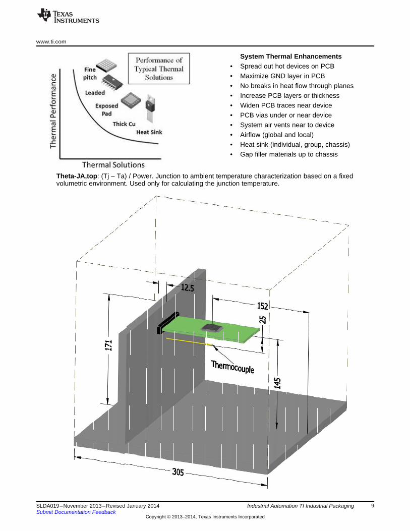
System Thermal Enhancements• Spread out hot devices on PCB• Maximize GND layer in PCB• No breaks in heat flow through planes• Increase PCB layers or thickness• Widen PCB traces near device• PCB vias under or near device• System air vents near to device• Airflow (global and local)• Heat sink (individual, group, chassis)• Gap filler materials up to chassis
Theta-JA,top: (Tj – Ta) / Power. Junction to ambient temperature characterization based on a fixedvolumetric environment. Used only for calculating the junction temperature.
9SLDA019–November 2013–Revised January 2014 Industrial Automation TI Industrial PackagingSubmit Documentation Feedback
Copyright © 2013–2014, Texas Instruments Incorporated

www.ti.com
Theta-JB,Board: (Tj – Tb) / Power. The true thermal resistance to lead of the package. Used only forcalculating the flow of heat up at the leads.
Figure 9. Thermal Measurement Method
Theta-JC,top: (Tj – Tc) / Power. The true thermal resistance to the top of a package. Used only forcalculating the flow of heat up to a heat sink.
Figure 10. Cu Cold Plate Measurement Process
10 Industrial Automation TI Industrial Packaging SLDA019–November 2013–Revised January 2014Submit Documentation Feedback
Copyright © 2013–2014, Texas Instruments Incorporated
www.ti.com
11SLDA019–November 2013–Revised January 2014 Industrial Automation TI Industrial PackagingSubmit Documentation Feedback
Copyright © 2013–2014, Texas Instruments Incorporated
www.ti.com
12 Industrial Automation TI Industrial Packaging SLDA019–November 2013–Revised January 2014Submit Documentation Feedback
Copyright © 2013–2014, Texas Instruments Incorporated

www.ti.com
13SLDA019–November 2013–Revised January 2014 Industrial Automation TI Industrial PackagingSubmit Documentation Feedback
Copyright © 2013–2014, Texas Instruments Incorporated

www.ti.com
14 Industrial Automation TI Industrial Packaging SLDA019–November 2013–Revised January 2014Submit Documentation Feedback
Copyright © 2013–2014, Texas Instruments Incorporated

www.ti.com
15SLDA019–November 2013–Revised January 2014 Industrial Automation TI Industrial PackagingSubmit Documentation Feedback
Copyright © 2013–2014, Texas Instruments Incorporated

www.ti.com
16 Industrial Automation TI Industrial Packaging SLDA019–November 2013–Revised January 2014Submit Documentation Feedback
Copyright © 2013–2014, Texas Instruments Incorporated

www.ti.com
17SLDA019–November 2013–Revised January 2014 Industrial Automation TI Industrial PackagingSubmit Documentation Feedback
Copyright © 2013–2014, Texas Instruments Incorporated

www.ti.com
18 Industrial Automation TI Industrial Packaging SLDA019–November 2013–Revised January 2014Submit Documentation Feedback
Copyright © 2013–2014, Texas Instruments Incorporated

www.ti.com
19SLDA019–November 2013–Revised January 2014 Industrial Automation TI Industrial PackagingSubmit Documentation Feedback
Copyright © 2013–2014, Texas Instruments Incorporated

IMPORTANT NOTICETexas Instruments Incorporated and its subsidiaries (TI) reserve the right to make corrections, enhancements, improvements and otherchanges to its semiconductor products and services per JESD46, latest issue, and to discontinue any product or service per JESD48, latestissue. Buyers should obtain the latest relevant information before placing orders and should verify that such information is current andcomplete. All semiconductor products (also referred to herein as “components”) are sold subject to TI’s terms and conditions of salesupplied at the time of order acknowledgment.TI warrants performance of its components to the specifications applicable at the time of sale, in accordance with the warranty in TI’s termsand conditions of sale of semiconductor products. Testing and other quality control techniques are used to the extent TI deems necessaryto support this warranty. Except where mandated by applicable law, testing of all parameters of each component is not necessarilyperformed.TI assumes no liability for applications assistance or the design of Buyers’ products. Buyers are responsible for their products andapplications using TI components. To minimize the risks associated with Buyers’ products and applications, Buyers should provideadequate design and operating safeguards.TI does not warrant or represent that any license, either express or implied, is granted under any patent right, copyright, mask work right, orother intellectual property right relating to any combination, machine, or process in which TI components or services are used. Informationpublished by TI regarding third-party products or services does not constitute a license to use such products or services or a warranty orendorsement thereof. Use of such information may require a license from a third party under the patents or other intellectual property of thethird party, or a license from TI under the patents or other intellectual property of TI.Reproduction of significant portions of TI information in TI data books or data sheets is permissible only if reproduction is without alterationand is accompanied by all associated warranties, conditions, limitations, and notices. TI is not responsible or liable for such altereddocumentation. Information of third parties may be subject to additional restrictions.Resale of TI components or services with statements different from or beyond the parameters stated by TI for that component or servicevoids all express and any implied warranties for the associated TI component or service and is an unfair and deceptive business practice.TI is not responsible or liable for any such statements.Buyer acknowledges and agrees that it is solely responsible for compliance with all legal, regulatory and safety-related requirementsconcerning its products, and any use of TI components in its applications, notwithstanding any applications-related information or supportthat may be provided by TI. Buyer represents and agrees that it has all the necessary expertise to create and implement safeguards whichanticipate dangerous consequences of failures, monitor failures and their consequences, lessen the likelihood of failures that might causeharm and take appropriate remedial actions. Buyer will fully indemnify TI and its representatives against any damages arising out of the useof any TI components in safety-critical applications.In some cases, TI components may be promoted specifically to facilitate safety-related applications. With such components, TI’s goal is tohelp enable customers to design and create their own end-product solutions that meet applicable functional safety standards andrequirements. Nonetheless, such components are subject to these terms.No TI components are authorized for use in FDA Class III (or similar life-critical medical equipment) unless authorized officers of the partieshave executed a special agreement specifically governing such use.Only those TI components which TI has specifically designated as military grade or “enhanced plastic” are designed and intended for use inmilitary/aerospace applications or environments. Buyer acknowledges and agrees that any military or aerospace use of TI componentswhich have not been so designated is solely at the Buyer's risk, and that Buyer is solely responsible for compliance with all legal andregulatory requirements in connection with such use.TI has specifically designated certain components as meeting ISO/TS16949 requirements, mainly for automotive use. In any case of use ofnon-designated products, TI will not be responsible for any failure to meet ISO/TS16949.Products ApplicationsAudio www.ti.com/audio Automotive and Transportation www.ti.com/automotiveAmplifiers amplifier.ti.com Communications and Telecom www.ti.com/communicationsData Converters dataconverter.ti.com Computers and Peripherals www.ti.com/computersDLP® Products www.dlp.com Consumer Electronics www.ti.com/consumer-appsDSP dsp.ti.com Energy and Lighting www.ti.com/energyClocks and Timers www.ti.com/clocks Industrial www.ti.com/industrialInterface interface.ti.com Medical www.ti.com/medicalLogic logic.ti.com Security www.ti.com/securityPower Mgmt power.ti.com Space, Avionics and Defense www.ti.com/space-avionics-defenseMicrocontrollers microcontroller.ti.com Video and Imaging www.ti.com/videoRFID www.ti-rfid.comOMAP Applications Processors www.ti.com/omap TI E2E Community e2e.ti.comWireless Connectivity www.ti.com/wirelessconnectivity
Mailing Address: Texas Instruments, Post Office Box 655303, Dallas, Texas 75265Copyright © 2014, Texas Instruments Incorporated