In this chapter, you will - LumiDaxChapter 7.2: Boolean Algebra Before we dive into playing with...
41
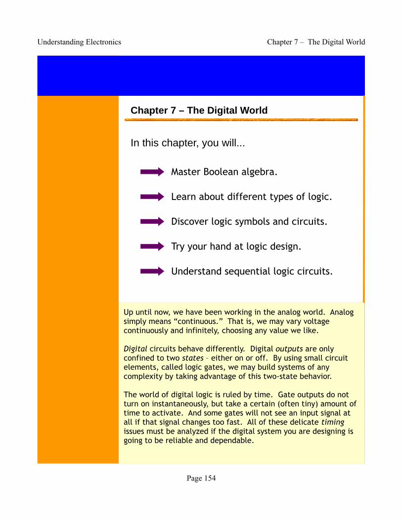
Understanding Electronics Chapter 7 – The Digital World Chapter 7 – The Digital World In this chapter, you will... Page 154 Master Boolean algebra. Discover logic symbols and circuits. Learn about different types of logic. Try your hand at logic design. Understand sequential logic circuits. Up until now, we have been working in the analog world. Analog simply means “continuous.” That is, we may vary voltage continuously and infinitely, choosing any value we like. Digital circuits behave differently. Digital outputs are only confined to two states – either on or off. By using small circuit elements, called logic gates, we may build systems of any complexity by taking advantage of this two-state behavior. The world of digital logic is ruled by time. Gate outputs do not turn on instantaneously, but take a certain (often tiny) amount of time to activate. And some gates will not see an input signal at all if that signal changes too fast. All of these delicate timing issues must be analyzed if the digital system you are designing is going to be reliable and dependable.
Transcript of In this chapter, you will - LumiDaxChapter 7.2: Boolean Algebra Before we dive into playing with...
Understanding Electronics Chapter 7 – The Digital World
Chapter 7 – The Digital World
In this chapter, you will...
Page 154
Master Boolean algebra.
Discover logic symbols and circuits.
Learn about different types of logic.
Try your hand at logic design.
Understand sequential logic circuits.
Up until now, we have been working in the analog world. Analog simply means “continuous.” That is, we may vary voltage continuously and infinitely, choosing any value we like.
Digital circuits behave differently. Digital outputs are only confined to two states – either on or off. By using small circuit elements, called logic gates, we may build systems of any complexity by taking advantage of this two-state behavior.
The world of digital logic is ruled by time. Gate outputs do not turn on instantaneously, but take a certain (often tiny) amount of time to activate. And some gates will not see an input signal at all if that signal changes too fast. All of these delicate timing issues must be analyzed if the digital system you are designing is going to be reliable and dependable.

Understanding Electronics Chapter 7 – The Digital World
Chapter 7.1: A Brief Not So Brief History of Digital Logic
The history of digital logic is not as short as you might think. The concept of solving problems using
symbols originated in Persia, with al-Khwarizmi's writings detailing how to solve algebraic problems
using algorithms, circa 800 C.E. In the 1800s, mechanical gears and switches were used to build
calculating machines. The advancements in radio technology in the 1910s led to the development of
tube devices; However, the invention of the bipolar junction transistor in 1947 changed everything.
Chapter 7.2: Boolean Algebra
Before we dive into playing with logic ICs and push-button switches, we need to go over a little theory
first. Boolean algebra gives us a list of rules for how a logic gate will behave for a set of given inputs,
and how to design digital circuits using Boolean expressions. Each type of gate has a special name,
and by combining the different types of gates together, we may construct even more complex
functions. Therefore, knowing how to solve Boolean expressions will make design much easier.
What is Boolean Algebra?
Just as with ordinary high-school algebra, we may devise a symbolic system such that we may
minimize (factor) expressions and solve for unknowns involving Boolean values. When we say the
word Boolean, we are referring to the fact that our “variables” may take on only two values in the set
{ 0, 1 }. That is, a variable can either be ON or OFF (TRUE or FALSE, respectively.) There is no in-
between state, and no “2.” We will cover number systems and binary arithmetic later in this chapter.
Positive vs. Negative Logic
As we have just stated, logic variables may have one of two states. By convention, we use ON (1) as
logic high and OFF (0) as logic low. This is referred to as positive logic. However, we may also make
the OFF state (0) represent logic high and the ON state logic low. When the roles are reversed in this
way, we are said to be using negative logic. Both systems are used in electronics. For example, the
IC you are using may have positive logic inputs and outputs for data, but negative logic inputs for
controlling the various functions of the IC. It is very common, so be sure to pay attention!
Page 155
Understanding Electronics Chapter 7 – The Digital World
Boolean Operators
A Boolean operator is just like any algebraic operator. In algebra, we have addition ( + ), subtraction
( - ), multiplication ( * or X ) and division ( / ), and these operators tell us how to calculate the result.
Not surprisingly, we may find analogs (pun intended) to these operations in Boolean algebra: we have
an operation very similar to addition, which is represented by the OR operator, represented by a plus
sign ( A + B, say “A or B.” ) And we may also “multiply” Boolean values together with the AND
operator ( A * B, say “A and B.” ) Instead of a negative sign, we may negate with bar notation or with
an exclamation point ( A, !A , say “A-bar” or “not A.” ) Finally, we have a sort of oddball function called
exclusive OR, which can be built using the other functions. Exclusive OR is represented by a circle
with a plus inside ( ), and is a specialized form of the OR function.
Properties of Boolean Expressions
In the table shown below, we outline the basic properties and laws of Boolean algebra. Notice some
of the similarities to laws you already know with regards to numeric expressions. Memorize the
contents of this table. It will be on the midterm. Just kidding.
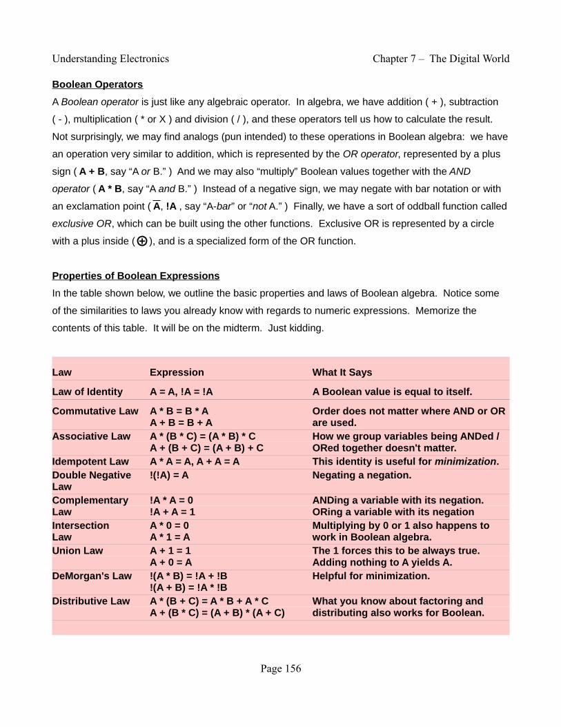
Law Expression What It Says
Law of Identity A = A, !A = !A A Boolean value is equal to itself.
Commutative Law A * B = B * A Order does not matter where AND or OR A + B = B + A are used.
Associative Law A * (B * C) = (A * B) * C How we group variables being ANDed /A + (B + C) = (A + B) + C ORed together doesn't matter.
Idempotent Law A * A = A, A + A = A This identity is useful for minimization.Double Negative !(!A) = A Negating a negation.LawComplementary !A * A = 0 ANDing a variable with its negation.Law !A + A = 1 ORing a variable with its negationIntersection A * 0 = 0 Multiplying by 0 or 1 also happens toLaw A * 1 = A work in Boolean algebra.Union Law A + 1 = 1 The 1 forces this to be always true.
A + 0 = A Adding nothing to A yields A.DeMorgan's Law !(A * B) = !A + !B Helpful for minimization.
!(A + B) = !A * !BDistributive Law A * (B + C) = A * B + A * C What you know about factoring and
A + (B * C) = (A + B) * (A + C) distributing also works for Boolean.
Page 156
+
Understanding Electronics Chapter 7 – The Digital World
Chapter 7.3: Introduction to Logic Gates
Logic gates are electronic circuits that implement Boolean operations. They are the building blocks of
combinational logic. Combinational logic tells us how to combine basic Boolean functions to obtain
more complicated behavior. Logic gates produce an output instantaneously when their inputs change.
That is, logic gates are time-independent; the output is purely a function of the present input state(s.)
The Logic Buffer Gate
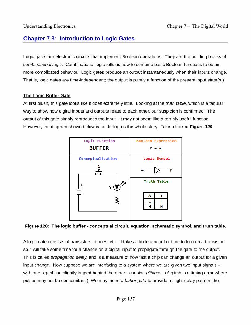
At first blush, this gate looks like it does extremely little. Looking at the truth table, which is a tabular
way to show how digital inputs and outputs relate to each other, our suspicion is confirmed. The
output of this gate simply reproduces the input. It may not seem like a terribly useful function.
However, the diagram shown below is not telling us the whole story. Take a look at Figure 120.
Figure 120: The logic buffer - conceptual circuit, equation, schematic symbol, and truth table.
A logic gate consists of transistors, diodes, etc. It takes a finite amount of time to turn on a transistor,
so it will take some time for a change on a digital input to propagate through the gate to the output.
This is called propagation delay, and is a measure of how fast a chip can change an output for a given
input change. Now suppose we are interfacing to a system where we are given two input signals –
with one signal line slightly lagged behind the other - causing glitches. (A glitch is a timing error where
pulses may not be concomitant.) We may insert a buffer gate to provide a slight delay path on the
Page 157
Understanding Electronics Chapter 7 – The Digital World
faster signal to correct the problem. Another use of logic buffers is where we must feed many logic
inputs with only one output, or as a line driver to transmit data. Logic gates really aren't designed for
driving more than a few mA of current. If there are a lot of logic gates in the system, your logic output
may have to fan out to perhaps even hundreds of other inputs. If the output cannot source (act as
Vcc) or sink (act as ground) the current required, a buffer with greater drive capability can be used for
this output to boost the fan-out capability. A TTL hex-buffer is the 74LS07 (open-collector driver.)
The Inverter Gate
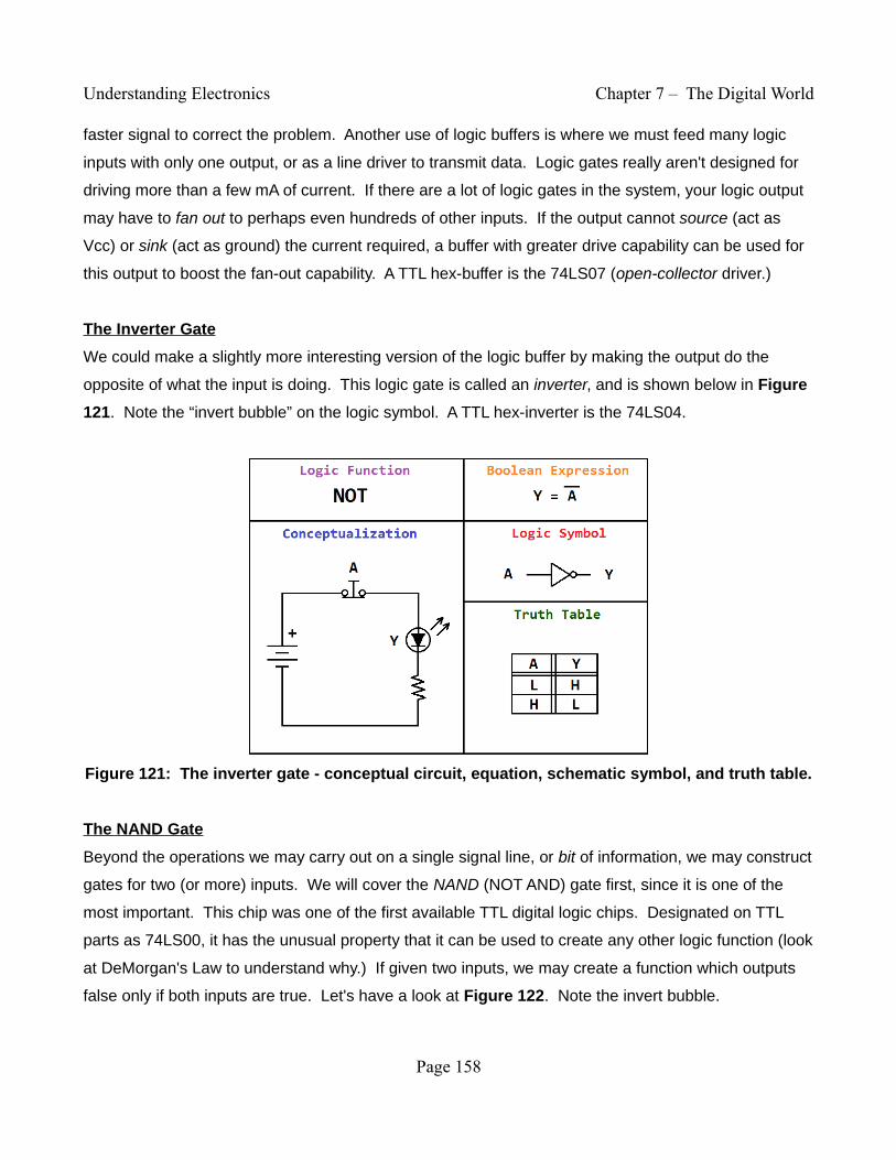
We could make a slightly more interesting version of the logic buffer by making the output do the
opposite of what the input is doing. This logic gate is called an inverter, and is shown below in Figure
121. Note the “invert bubble” on the logic symbol. A TTL hex-inverter is the 74LS04.
Figure 121: The inverter gate - conceptual circuit, equation, schematic symbol, and truth table.
The NAND Gate
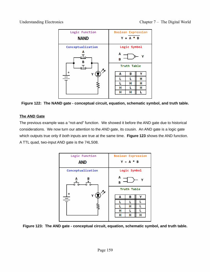
Beyond the operations we may carry out on a single signal line, or bit of information, we may construct
gates for two (or more) inputs. We will cover the NAND (NOT AND) gate first, since it is one of the
most important. This chip was one of the first available TTL digital logic chips. Designated on TTL
parts as 74LS00, it has the unusual property that it can be used to create any other logic function (look
at DeMorgan's Law to understand why.) If given two inputs, we may create a function which outputs
false only if both inputs are true. Let's have a look at Figure 122. Note the invert bubble.
Page 158
Understanding Electronics Chapter 7 – The Digital World
Figure 122: The NAND gate - conceptual circuit, equation, schematic symbol, and truth table.
The AND Gate
The previous example was a “not-and” function. We showed it before the AND gate due to historical
considerations. We now turn our attention to the AND gate, its cousin. An AND gate is a logic gate
which outputs true only if both inputs are true at the same time. Figure 123 shows the AND function.
A TTL quad, two-input AND gate is the 74LS08.
Figure 123: The AND gate - conceptual circuit, equation, schematic symbol, and truth table.
Page 159
Understanding Electronics Chapter 7 – The Digital World
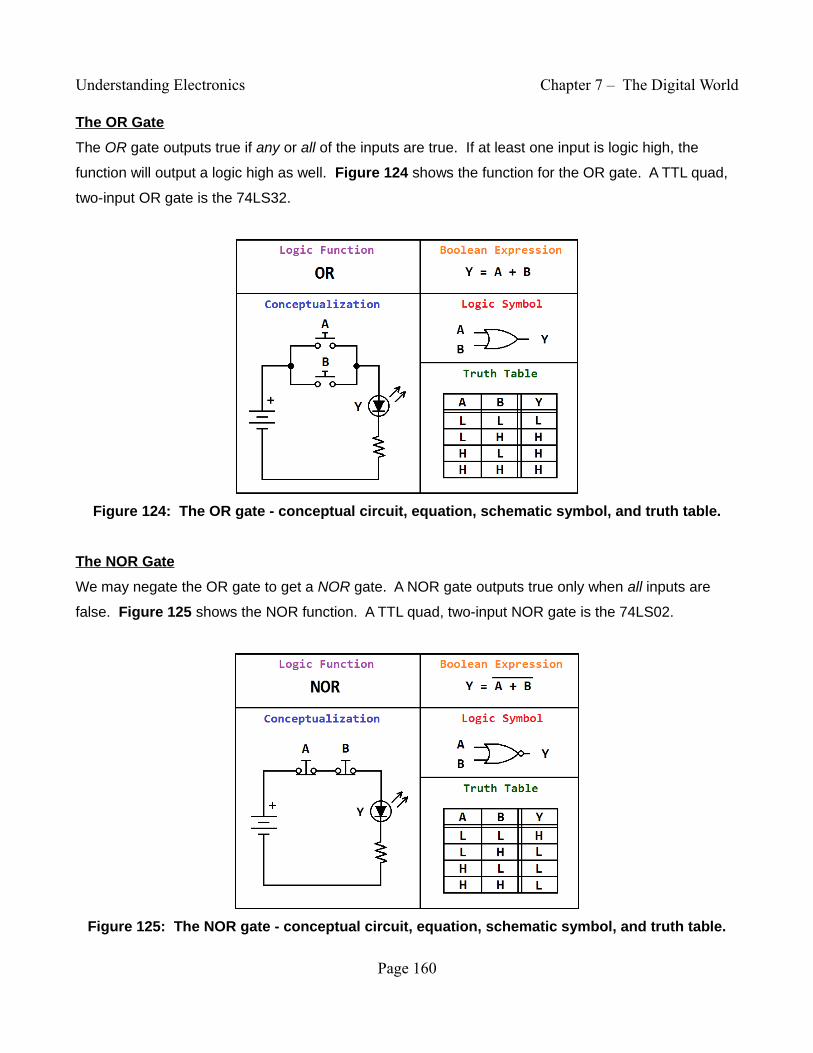
The OR Gate
The OR gate outputs true if any or all of the inputs are true. If at least one input is logic high, the
function will output a logic high as well. Figure 124 shows the function for the OR gate. A TTL quad,
two-input OR gate is the 74LS32.
Figure 124: The OR gate - conceptual circuit, equation, schematic symbol, and truth table.
The NOR Gate
We may negate the OR gate to get a NOR gate. A NOR gate outputs true only when all inputs are
false. Figure 125 shows the NOR function. A TTL quad, two-input NOR gate is the 74LS02.
Figure 125: The NOR gate - conceptual circuit, equation, schematic symbol, and truth table.
Page 160
Understanding Electronics Chapter 7 – The Digital World
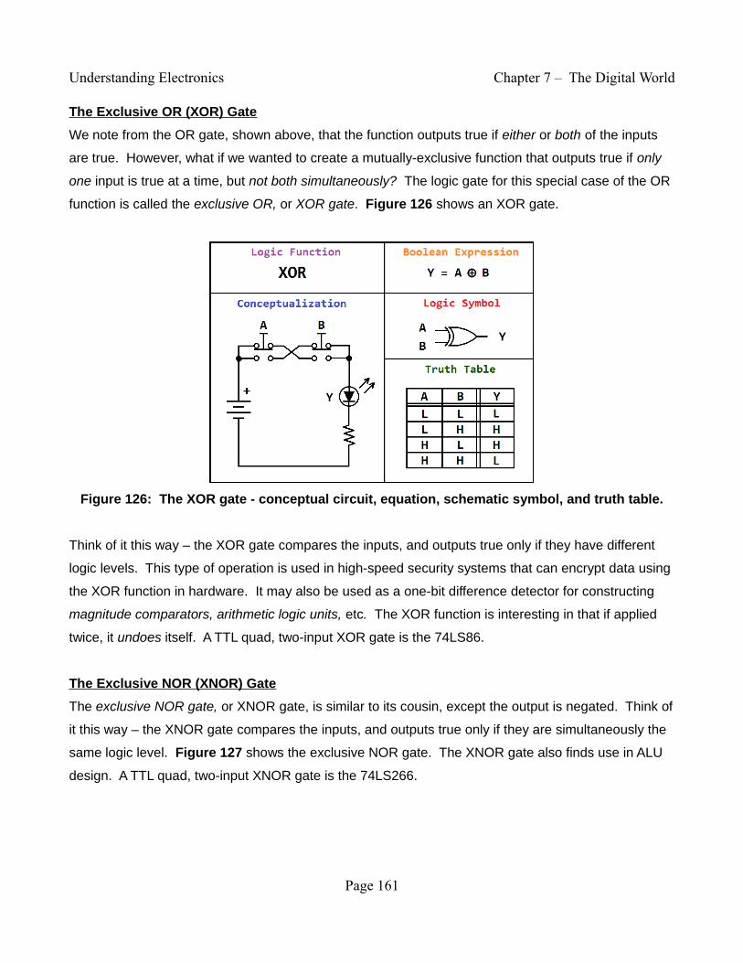
The Exclusive OR (XOR) Gate
We note from the OR gate, shown above, that the function outputs true if either or both of the inputs
are true. However, what if we wanted to create a mutually-exclusive function that outputs true if only
one input is true at a time, but not both simultaneously? The logic gate for this special case of the OR
function is called the exclusive OR, or XOR gate. Figure 126 shows an XOR gate.
Figure 126: The XOR gate - conceptual circuit, equation, schematic symbol, and truth table.
Think of it this way – the XOR gate compares the inputs, and outputs true only if they have different
logic levels. This type of operation is used in high-speed security systems that can encrypt data using
the XOR function in hardware. It may also be used as a one-bit difference detector for constructing
magnitude comparators, arithmetic logic units, etc. The XOR function is interesting in that if applied
twice, it undoes itself. A TTL quad, two-input XOR gate is the 74LS86.
The Exclusive NOR (XNOR) Gate
The exclusive NOR gate, or XNOR gate, is similar to its cousin, except the output is negated. Think of
it this way – the XNOR gate compares the inputs, and outputs true only if they are simultaneously the
same logic level. Figure 127 shows the exclusive NOR gate. The XNOR gate also finds use in ALU
design. A TTL quad, two-input XNOR gate is the 74LS266.
Page 161

Understanding Electronics Chapter 7 – The Digital World
Figure 127: The XNOR gate - conceptual circuit, equation, schematic symbol, and truth table.
Chapter 7.4: Combinational Logic Design and Minimization
We have covered the basic properties of Boolean algebra and have introduced logic gates. Now we
will begin exploring digital design concepts and minimization techniques. Minimization is an important
area of study in digital design. By using minimization techniques, the goal is always to make the
system you are designing as small as possible with the fewest number of logic gates. If the same
function can be done with fewer gates, not only do you save money, but time, board space, etc.
Designing with Truth Tables and Algebraic Minimization
Just as numeric expressions can be factored and simplified in algebra, we may employ the same
techniques to simplify Boolean algebraic expressions. We'll start with an easy design example to get
a feel for the process, and an understanding of why minimization is important.
Design Example 1
Suppose you are designing an alarm system for a house that has one door and one window. The
alarm siren sounds when the system is armed and the front door opens, or when the system is armed
and the window is open, or both cases. Write a truth table, Boolean equation, and draw the circuit.
Page 162
Understanding Electronics Chapter 7 – The Digital World
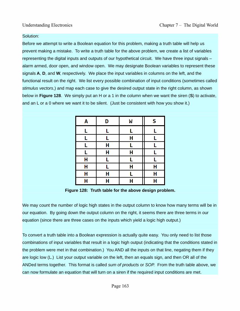
Solution:
Before we attempt to write a Boolean equation for this problem, making a truth table will help us
prevent making a mistake. To write a truth table for the above problem, we create a list of variables
representing the digital inputs and outputs of our hypothetical circuit. We have three input signals –
alarm armed, door open, and window open. We may designate Boolean variables to represent these
signals A, D, and W, respectively. We place the input variables in columns on the left, and the
functional result on the right. We list every possible combination of input conditions (sometimes called
stimulus vectors,) and map each case to give the desired output state in the right column, as shown
below in Figure 128. We simply put an H or a 1 in the column when we want the siren (S) to activate,
and an L or a 0 where we want it to be silent. (Just be consistent with how you show it.)
Figure 128: Truth table for the above design problem.
We may count the number of logic high states in the output column to know how many terms will be in
our equation. By going down the output column on the right, it seems there are three terms in our
equation (since there are three cases on the inputs which yield a logic high output.)
To convert a truth table into a Boolean expression is actually quite easy. You only need to list those
combinations of input variables that result in a logic high output (indicating that the conditions stated in
the problem were met in that combination.) You AND all the inputs on that line, negating them if they
are logic low (L.) List your output variable on the left, then an equals sign, and then OR all of the
ANDed terms together. This format is called sum of products or SOP. From the truth table above, we
can now formulate an equation that will turn on a siren if the required input conditions are met.
Page 163
Understanding Electronics Chapter 7 – The Digital World
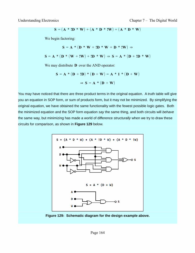
S = (A * !D * W) + (A * D * !W) + (A * D * W)
We begin factoring:
S = A * (D * W + !D * W + D * !W) ⇒
S = A * (D * (W + !W) + !D * W) ⇒ S = A * (D + !D * W)
We may distribute D over the AND operator:
S = A * (D + !D) * (D + W) = A * 1 * (D + W)
⇒ S = A * (D + W)
You may have noticed that there are three product terms in the original equation. A truth table will give
you an equation in SOP form, or sum of products form, but it may not be minimized. By simplifying the
original equation, we have obtained the same functionality with the fewest possible logic gates. Both
the minimized equation and the SOP form equation say the same thing, and both circuits will behave
the same way, but minimizing has made a world of difference structurally when we try to draw these
circuits for comparison, as shown in Figure 129 below.
Figure 129: Schematic diagram for the design example above.
Page 164

Understanding Electronics Chapter 7 – The Digital World
Further Minimization Techniques
It is unfortunate that we can end up with at most eight product terms in our equation for only three
input variables. That is a lot of factoring to do by hand to arrive at the minimized equation for so few
inputs. One may get lucky depending on the circumstances. However, dealing with more than three
input variables makes for a nasty set of factoring. Four variables means up to 16 product terms in our
resultant Boolean equation, and five variables yields a Boolean equation with up to 32 product terms.
What to say of larger systems such as a data bus?
Constructing Karnaugh Maps from Truth Tables
If we have four or more variables, we may want to consider using a Karnaugh map (say “KAR - no”).
They are a little cumbersome to set up, but produce elegant results. Furthermore, Karnaugh maps
also show us additional information, such as the existence of race conditions (structural glitches
caused by propagation delay.) We will explore three-variable and four-variable Karnaugh maps. Let's
take a look at Figure 130 to get an idea of how a Karnaugh map works. We'll start with the three
variable system we covered in Design Example 1. We will use the truth table to populate the
Karnaugh map and demonstrate that it generates minimized Boolean equations.
Figure 130: A three-variable Karnaugh map representation of Design Example 1.
We construct a truth table and begin looking for those patterns of A, D, and W, that yield a high (or
true) output. Then, we make a grid of either 4X2 or 4X4, depending on the number of input variables.
In the case of Design Example 1, we have three input variables, therefore we need a 4X2 map. We
label the variables in groups of two at most, such that all input variables are represented exactly once
Page 165
Understanding Electronics Chapter 7 – The Digital World
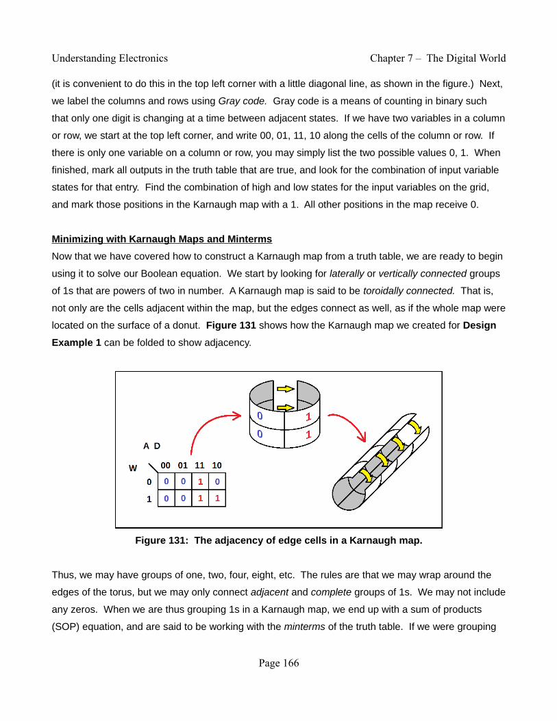
(it is convenient to do this in the top left corner with a little diagonal line, as shown in the figure.) Next,
we label the columns and rows using Gray code. Gray code is a means of counting in binary such
that only one digit is changing at a time between adjacent states. If we have two variables in a column
or row, we start at the top left corner, and write 00, 01, 11, 10 along the cells of the column or row. If
there is only one variable on a column or row, you may simply list the two possible values 0, 1. When
finished, mark all outputs in the truth table that are true, and look for the combination of input variable
states for that entry. Find the combination of high and low states for the input variables on the grid,
and mark those positions in the Karnaugh map with a 1. All other positions in the map receive 0.
Minimizing with Karnaugh Maps and Minterms
Now that we have covered how to construct a Karnaugh map from a truth table, we are ready to begin
using it to solve our Boolean equation. We start by looking for laterally or vertically connected groups
of 1s that are powers of two in number. A Karnaugh map is said to be toroidally connected. That is,
not only are the cells adjacent within the map, but the edges connect as well, as if the whole map were
located on the surface of a donut. Figure 131 shows how the Karnaugh map we created for Design
Example 1 can be folded to show adjacency.
Figure 131: The adjacency of edge cells in a Karnaugh map.
Thus, we may have groups of one, two, four, eight, etc. The rules are that we may wrap around the
edges of the torus, but we may only connect adjacent and complete groups of 1s. We may not include
any zeros. When we are thus grouping 1s in a Karnaugh map, we end up with a sum of products
(SOP) equation, and are said to be working with the minterms of the truth table. If we were grouping
Page 166
Understanding Electronics Chapter 7 – The Digital World
zeros, we would be working instead with maxterms, and have a Boolean equation of a different form
(product of sums or POS.) It should be noted that to use maxterms is a different process and is
beyond the scope of this text. We will only cover solving for the minterms of a truth table, and leave
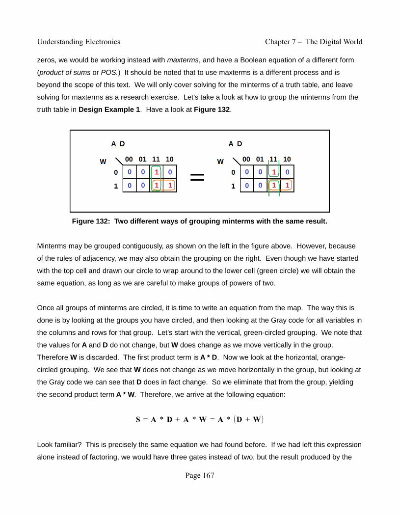
solving for maxterms as a research exercise. Let's take a look at how to group the minterms from the
truth table in Design Example 1. Have a look at Figure 132.
Figure 132: Two different ways of grouping minterms with the same result.
Minterms may be grouped contiguously, as shown on the left in the figure above. However, because
of the rules of adjacency, we may also obtain the grouping on the right. Even though we have started
with the top cell and drawn our circle to wrap around to the lower cell (green circle) we will obtain the
same equation, as long as we are careful to make groups of powers of two.
Once all groups of minterms are circled, it is time to write an equation from the map. The way this is
done is by looking at the groups you have circled, and then looking at the Gray code for all variables in
the columns and rows for that group. Let's start with the vertical, green-circled grouping. We note that
the values for A and D do not change, but W does change as we move vertically in the group.
Therefore W is discarded. The first product term is A * D. Now we look at the horizontal, orange-
circled grouping. We see that W does not change as we move horizontally in the group, but looking at
the Gray code we can see that D does in fact change. So we eliminate that from the group, yielding
the second product term A * W. Therefore, we arrive at the following equation:
S = A * D + A * W = A * (D + W)
Look familiar? This is precisely the same equation we had found before. If we had left this expression
alone instead of factoring, we would have three gates instead of two, but the result produced by the
Page 167
Understanding Electronics Chapter 7 – The Digital World
Karnaugh map is more symmetrical. Therefore, the Karnaugh map has bypassed a lot of the steps we
had to take algebraically, making the problem far more manageable. When doing Karnaugh maps for
five variables, two 4x4 grids are required. But for six variables, we obtain a 4X4X4 Karnaugh map,
which requires an additional two 4X4 maps. But even at five input variables, we must think of
grouping minterms in three-dimensional space, which is challenging. Keep it in mind.
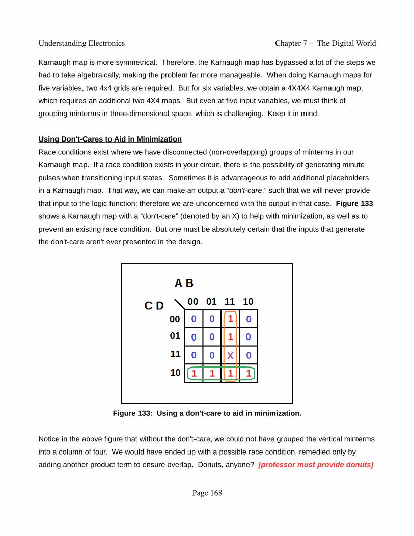
Using Don't-Cares to Aid in Minimization
Race conditions exist where we have disconnected (non-overlapping) groups of minterms in our
Karnaugh map. If a race condition exists in your circuit, there is the possibility of generating minute
pulses when transitioning input states. Sometimes it is advantageous to add additional placeholders
in a Karnaugh map. That way, we can make an output a “don't-care,” such that we will never provide
that input to the logic function; therefore we are unconcerned with the output in that case. Figure 133
shows a Karnaugh map with a “don't-care” (denoted by an X) to help with minimization, as well as to
prevent an existing race condition. But one must be absolutely certain that the inputs that generate
the don't-care aren't ever presented in the design.
Figure 133: Using a don't-care to aid in minimization.
Notice in the above figure that without the don't-care, we could not have grouped the vertical minterms
into a column of four. We would have ended up with a possible race condition, remedied only by
adding another product term to ensure overlap. Donuts, anyone? [professor must provide donuts]
Page 168
Understanding Electronics Chapter 7 – The Digital World
Chapter 7.5: Number Systems
The Decimal, Binary, and Hexadecimal Number Systems
Most people are familiar with the base 10 number system, also known as the decimal number system.
Counting in base 10 is so very human, after all. The human body typically has 10 fingers. And the
number 10 has such wonderful properties. But did you ever wonder why? It is a pattern generated by
our choice of counting with 10 symbols.
In base 10 arithmetic, we may count physical objects or symbolic tokens by using the symbols in the
Arabic set of numerals {0, 1, 2, 3, 4, 5, 6, 7, 8, 9} to represent the count. The placement of digits
progresses from right to left for each power of 10 we add, such that the placement tells us how may
1s, 10s, 100s, etc., we need to build a number. So we may think of increasing powers of ten starting
at the rightmost (least significant) digit, starting with 100, 101, 102, etc., in each position as weights or
multipliers. News to you, right?
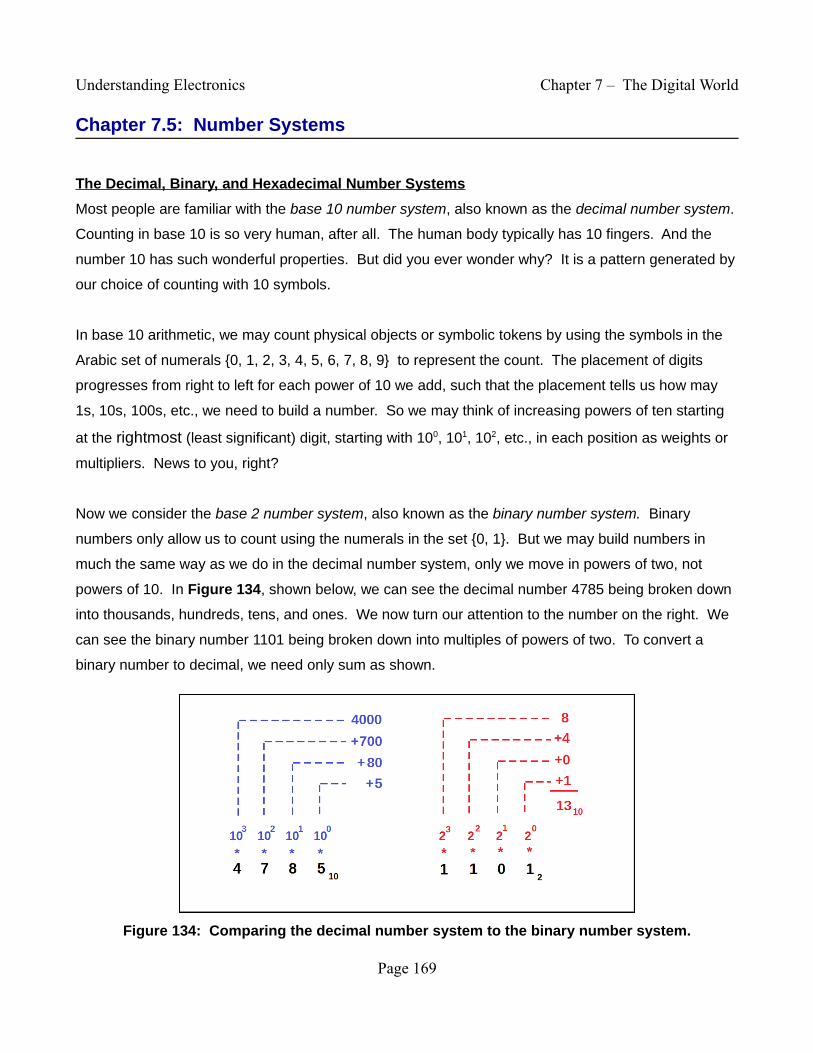
Now we consider the base 2 number system, also known as the binary number system. Binary
numbers only allow us to count using the numerals in the set {0, 1}. But we may build numbers in
much the same way as we do in the decimal number system, only we move in powers of two, not
powers of 10. In Figure 134, shown below, we can see the decimal number 4785 being broken down
into thousands, hundreds, tens, and ones. We now turn our attention to the number on the right. We
can see the binary number 1101 being broken down into multiples of powers of two. To convert a
binary number to decimal, we need only sum as shown.
Figure 134: Comparing the decimal number system to the binary number system.
Page 169
Understanding Electronics Chapter 7 – The Digital World
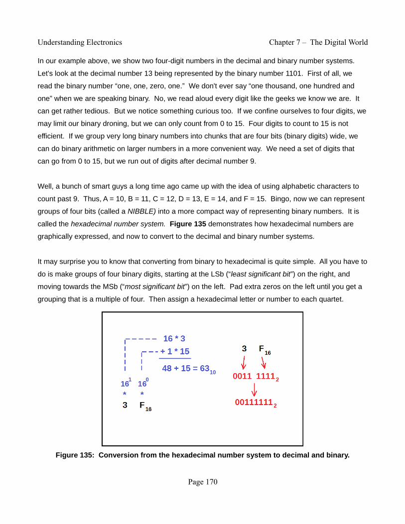
In our example above, we show two four-digit numbers in the decimal and binary number systems.
Let's look at the decimal number 13 being represented by the binary number 1101. First of all, we
read the binary number “one, one, zero, one.” We don't ever say “one thousand, one hundred and
one” when we are speaking binary. No, we read aloud every digit like the geeks we know we are. It
can get rather tedious. But we notice something curious too. If we confine ourselves to four digits, we
may limit our binary droning, but we can only count from 0 to 15. Four digits to count to 15 is not
efficient. If we group very long binary numbers into chunks that are four bits (binary digits) wide, we
can do binary arithmetic on larger numbers in a more convenient way. We need a set of digits that
can go from 0 to 15, but we run out of digits after decimal number 9.
Well, a bunch of smart guys a long time ago came up with the idea of using alphabetic characters to
count past 9. Thus, A = 10, B = 11, C = 12, D = 13, E = 14, and F = 15. Bingo, now we can represent
groups of four bits (called a NIBBLE) into a more compact way of representing binary numbers. It is
called the hexadecimal number system. Figure 135 demonstrates how hexadecimal numbers are
graphically expressed, and now to convert to the decimal and binary number systems.
It may surprise you to know that converting from binary to hexadecimal is quite simple. All you have to
do is make groups of four binary digits, starting at the LSb (“least significant bit”) on the right, and
moving towards the MSb (“most significant bit”) on the left. Pad extra zeros on the left until you get a
grouping that is a multiple of four. Then assign a hexadecimal letter or number to each quartet.
Figure 135: Conversion from the hexadecimal number system to decimal and binary.
Page 170
Understanding Electronics Chapter 7 – The Digital World
With a two digit hexadecimal number, we may count from 0 to 255. Not bad – we can not only
represent eight digits (bits) of a long binary number, but we can also count fairly high as well. This
convenient package of eight binary digits is called a BYTE. Therefore, a BYTE is simply a two-digit
hexadecimal number. A WORD consists of two bytes, equaling 16 total binary digits, and a DWORD
consists of four bytes, equaling 32 total binary digits. Those bearded fellows who are familiar with
microcontroller development will recognize these as standard bus widths.
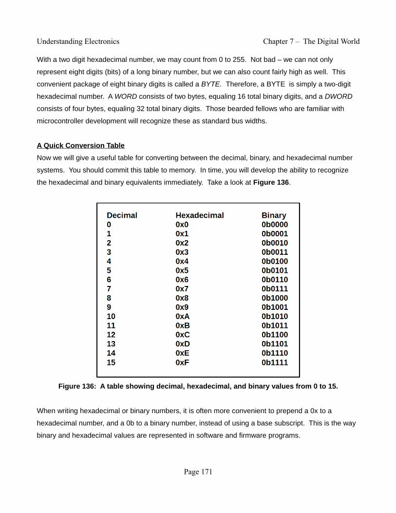
A Quick Conversion Table
Now we will give a useful table for converting between the decimal, binary, and hexadecimal number
systems. You should commit this table to memory. In time, you will develop the ability to recognize
the hexadecimal and binary equivalents immediately. Take a look at Figure 136.
Figure 136: A table showing decimal, hexadecimal, and binary values from 0 to 15.
When writing hexadecimal or binary numbers, it is often more convenient to prepend a 0x to a
hexadecimal number, and a 0b to a binary number, instead of using a base subscript. This is the way
binary and hexadecimal values are represented in software and firmware programs.
Page 171
Understanding Electronics Chapter 7 – The Digital World
Chapter 7.6: Finite State Machines
In Chapters 7.1 – 7.5, we discussed logic gates that are time-independent. Combinational logic gates
have no memory of their state. If you change the inputs, the outputs will also change instantaneously.
Sequential circuits are time-dependent, and have some form of timing mechanism (a clock,) a memory
for holding the present-state (registers or flip-flops,) a feedback network of combinational logic for the
next-state, and output logic. Such systems are generally referred to as finite state machines.
What Do Finite State Machines Do?
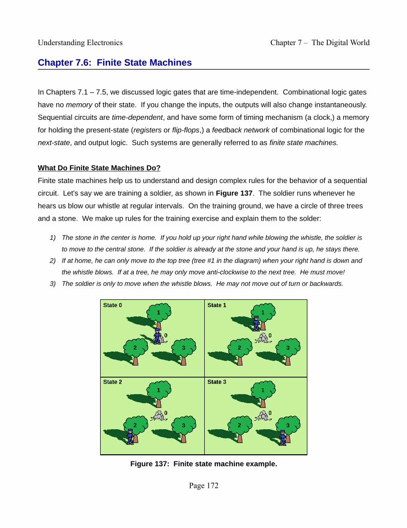
Finite state machines help us to understand and design complex rules for the behavior of a sequential
circuit. Let's say we are training a soldier, as shown in Figure 137. The soldier runs whenever he
hears us blow our whistle at regular intervals. On the training ground, we have a circle of three trees
and a stone. We make up rules for the training exercise and explain them to the solder:
1) The stone in the center is home. If you hold up your right hand while blowing the whistle, the soldier is
to move to the central stone. If the soldier is already at the stone and your hand is up, he stays there.
2) If at home, he can only move to the top tree (tree #1 in the diagram) when your right hand is down and
the whistle blows. If at a tree, he may only move anti-clockwise to the next tree. He must move!
3) The soldier is only to move when the whistle blows. He may not move out of turn or backwards.
Figure 137: Finite state machine example.
Page 172

Understanding Electronics Chapter 7 – The Digital World
The soldier in the above diagram can either be at the stone, or any of the three trees. Therefore, he
has exactly four states he can occupy. Our picture certainly helps us to understand where the soldier
may be standing, but not how he got there. We need a symbolic diagram that not only shows the
soldier's possible locations, but also how he may move from place to place.
State Transition Diagrams
We will now discuss state transition diagrams. We'll be using the solider example from Figure 137 to
draw a better representation of the rules we outlined in the previous section. We start by drawing
circles to represent our states and labeling them. Then, we connect the state bubbles with arrows
showing how we may transition from state to state. Finally, we label the arrows with the conditions
that allows for that transition. Figure 138 shows a state transition diagram for the example above.
Figure 138: A state transition diagram for the soldier problem.
From the figure, we see a more detailed picture of the rules for moving our soldier. Starting at state
S0, if we have our right hand down (H = 0,) there is only one place for the soldier to move – state S1.
From state S1, we may move to state S2 if H = 0, or we may move back to state S0 if H = 1, and so on.
Notice that state S0 is also an idle state (one of the arrows loops back on itself at state S0.) That is, we
remain at state S0 if H = 1. The example shown above is synchronous. That is, the soldier we are
training only moves when we blow our whistle. We might throw our right hand up while the soldier is
in motion, but he must finish moving to his destination along one of the transition arrows before the
next whistle. Only when he has arrived does he look at your hand for what to do next.
Page 173
Understanding Electronics Chapter 7 – The Digital World
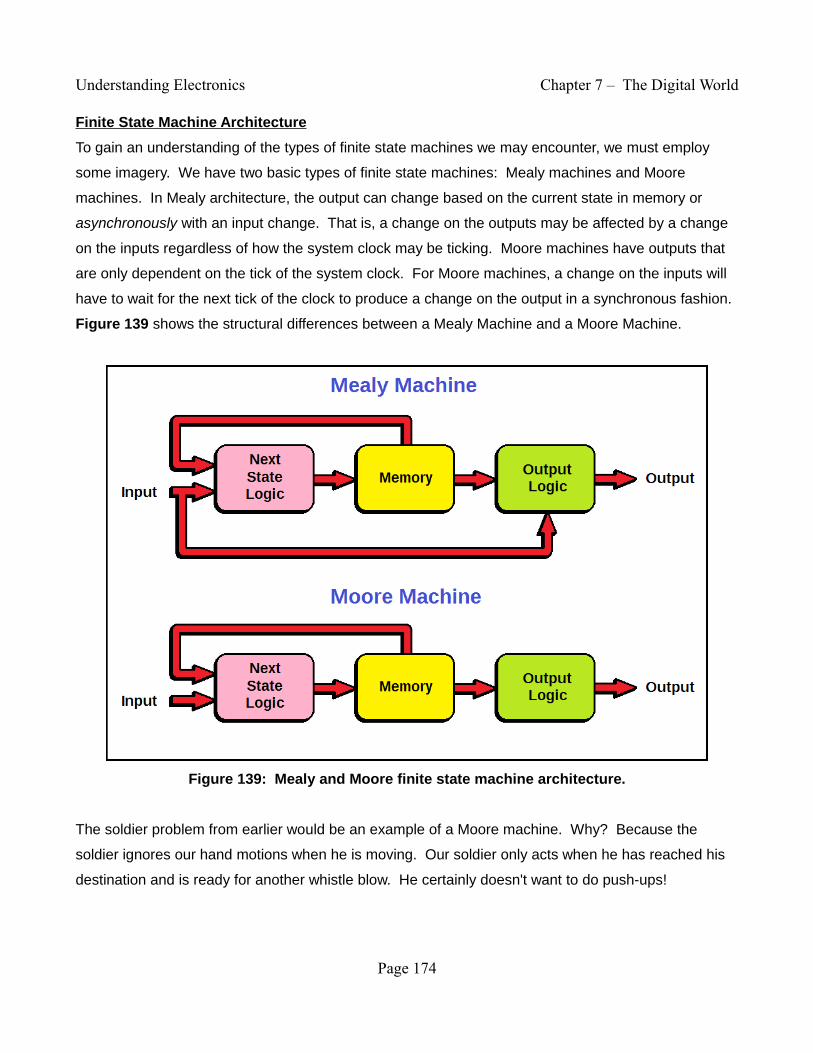
Finite State Machine Architecture
To gain an understanding of the types of finite state machines we may encounter, we must employ
some imagery. We have two basic types of finite state machines: Mealy machines and Moore
machines. In Mealy architecture, the output can change based on the current state in memory or
asynchronously with an input change. That is, a change on the outputs may be affected by a change
on the inputs regardless of how the system clock may be ticking. Moore machines have outputs that
are only dependent on the tick of the system clock. For Moore machines, a change on the inputs will
have to wait for the next tick of the clock to produce a change on the output in a synchronous fashion.
Figure 139 shows the structural differences between a Mealy Machine and a Moore Machine.
Figure 139: Mealy and Moore finite state machine architecture.
The soldier problem from earlier would be an example of a Moore machine. Why? Because the
soldier ignores our hand motions when he is moving. Our soldier only acts when he has reached his
destination and is ready for another whistle blow. He certainly doesn't want to do push-ups!
Page 174
Understanding Electronics Chapter 7 – The Digital World
Chapter 7.7: Latches and Flip-Flops
As we mentioned before, a finite state machine must have some form of memory to hold the present-
state. A flip-flop is a type of memory that can change states when given a pulse on an input, and can
store one bit of information. A register is a collection of one or more ordered bits (flip-flops) that
indicate a numeric value associated with a state in finite state machines.
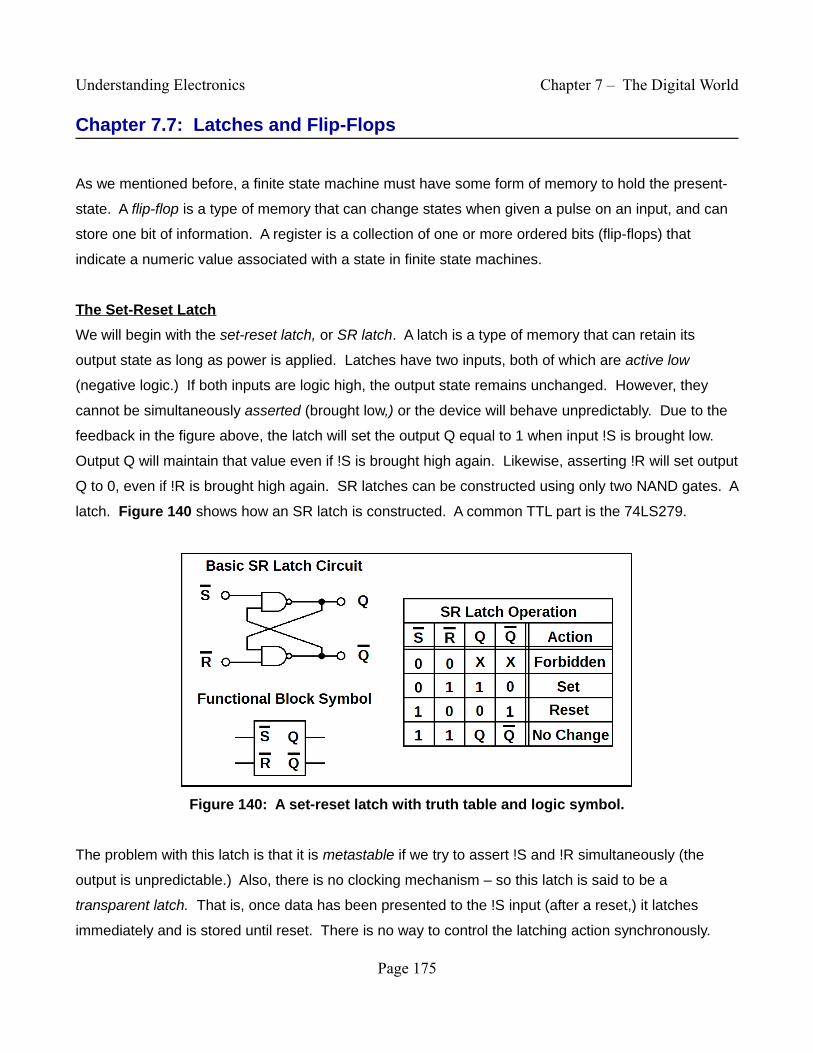
The Set-Reset Latch
We will begin with the set-reset latch, or SR latch. A latch is a type of memory that can retain its
output state as long as power is applied. Latches have two inputs, both of which are active low
(negative logic.) If both inputs are logic high, the output state remains unchanged. However, they
cannot be simultaneously asserted (brought low,) or the device will behave unpredictably. Due to the
feedback in the figure above, the latch will set the output Q equal to 1 when input !S is brought low.
Output Q will maintain that value even if !S is brought high again. Likewise, asserting !R will set output
Q to 0, even if !R is brought high again. SR latches can be constructed using only two NAND gates. A
latch. Figure 140 shows how an SR latch is constructed. A common TTL part is the 74LS279.
Figure 140: A set-reset latch with truth table and logic symbol.
The problem with this latch is that it is metastable if we try to assert !S and !R simultaneously (the
output is unpredictable.) Also, there is no clocking mechanism – so this latch is said to be a
transparent latch. That is, once data has been presented to the !S input (after a reset,) it latches
immediately and is stored until reset. There is no way to control the latching action synchronously.
Page 175

Understanding Electronics Chapter 7 – The Digital World
The Master-Slave JK Flip-Flop
The SR latch had some serious issues. The master-slave JK flip-flop is a huge improvement over the
SR latch: it uses two SR latches in tandem. A master-slave JK flip-flop requires a clock pulse to be
presented in order to latch the data. The JK flip-flop will not pass data from the master SR latch to the
slave until a rising edge occurs. On the next falling edge of the clock, the data is then latched to the
slave and all other changes are ignored until the next clock pulse. That makes the master-slave JK
flip-flop a negative edge triggered synchronous device. Like the SR latch, the JK flip-flop has both a
set function (J) and a reset function (K.) However, the inputs are active high (positive logic.)
Furthermore, it has no issues with forbidden states or requiring specialized pulse circuits. Figure 141
shows a master-slave JK flip-flop. A common master-slave JK flip-flop is the 74LS112.
Figure 141: A master-slave JK flip-flop with truth table and logic symbol.
An interesting point is that this flip-flop can toggle output states. If a logic high is presented to both J
and K when a clock pulse occurs, the master-slave JK flip-flop will invert output states. In other words,
it takes the data present at the output and negates it (flip-flop!) The master-slave JK flip-flop will be
revisited later, but we have one more type of register to learn about before we move on.
Page 176
Understanding Electronics Chapter 7 – The Digital World
The Master-Slave D Flip-Flop
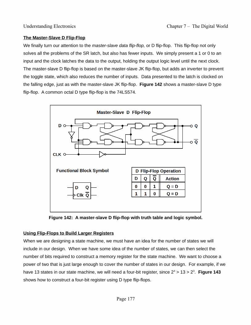
We finally turn our attention to the master-slave data flip-flop, or D flip-flop. This flip-flop not only
solves all the problems of the SR latch, but also has fewer inputs. We simply present a 1 or 0 to an
input and the clock latches the data to the output, holding the output logic level until the next clock.
The master-slave D flip-flop is based on the master-slave JK flip-flop, but adds an inverter to prevent
the toggle state, which also reduces the number of inputs. Data presented to the latch is clocked on
the falling edge, just as with the master-slave JK flip-flop. Figure 142 shows a master-slave D type
flip-flop. A common octal D type flip-flop is the 74LS574.
Figure 142: A master-slave D flip-flop with truth table and logic symbol.
Using Flip-Flops to Build Larger Registers
When we are designing a state machine, we must have an idea for the number of states we will
include in our design. When we have some idea of the number of states, we can then select the
number of bits required to construct a memory register for the state machine. We want to choose a
power of two that is just large enough to cover the number of states in our design. For example, if we
have 13 states in our state machine, we will need a four-bit register, since 24 > 13 > 23. Figure 143
shows how to construct a four-bit register using D type flip-flops.
Page 177

Understanding Electronics Chapter 7 – The Digital World
Figure 143: A four-bit register built with D flip-flops.
With the register shown above, it will be possible to latch four bits of input data simultaneously.
Complementary outputs are provided to ease the design requirements for the next-state logic.
Registers of any size may be constructed as above by ganging the clock inputs and adding flip-flops.
Chapter 7.8: Sequential Logic Design and Minimization
Now that we have shown how a set of flip-flops can be grouped to make a memory register, we can
move on to state machine implementation. The design process for sequential circuits is much like that
of combinational circuits. We must start with a specialized truth table that shows the inputs, the
present and next states, and any desired outputs. With this table, we use the present-state variables
to design feedback logic for the next state inputs.
Design Example 2
We will implement the soldier problem from earlier. The “whistle” will be a clock pulse, and our hand
up / down will be represented by a single input variable, H. Draw a state transition diagram and state-
table. Write Boolean equations for the feedback logic, and draw a schematic of your design.
Page 178
Understanding Electronics Chapter 7 – The Digital World
Solution:
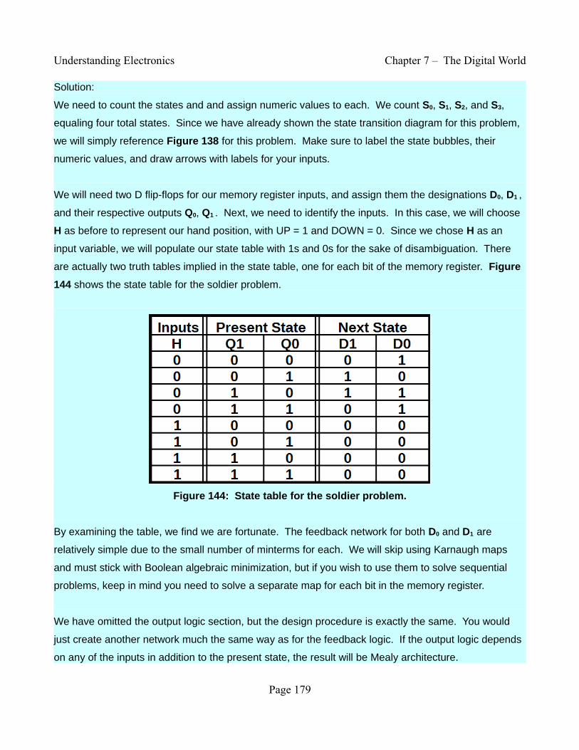
We need to count the states and and assign numeric values to each. We count S0, S1, S2, and S3,
equaling four total states. Since we have already shown the state transition diagram for this problem,
we will simply reference Figure 138 for this problem. Make sure to label the state bubbles, their
numeric values, and draw arrows with labels for your inputs.
We will need two D flip-flops for our memory register inputs, and assign them the designations D0, D1 ,
and their respective outputs Q0, Q1 . Next, we need to identify the inputs. In this case, we will choose
H as before to represent our hand position, with UP = 1 and DOWN = 0. Since we chose H as an
input variable, we will populate our state table with 1s and 0s for the sake of disambiguation. There
are actually two truth tables implied in the state table, one for each bit of the memory register. Figure
144 shows the state table for the soldier problem.
Figure 144: State table for the soldier problem.
By examining the table, we find we are fortunate. The feedback network for both D0 and D1 are
relatively simple due to the small number of minterms for each. We will skip using Karnaugh maps
and must stick with Boolean algebraic minimization, but if you wish to use them to solve sequential
problems, keep in mind you need to solve a separate map for each bit in the memory register.
We have omitted the output logic section, but the design procedure is exactly the same. You would
just create another network much the same way as for the feedback logic. If the output logic depends
on any of the inputs in addition to the present state, the result will be Mealy architecture.
Page 179
Understanding Electronics Chapter 7 – The Digital World
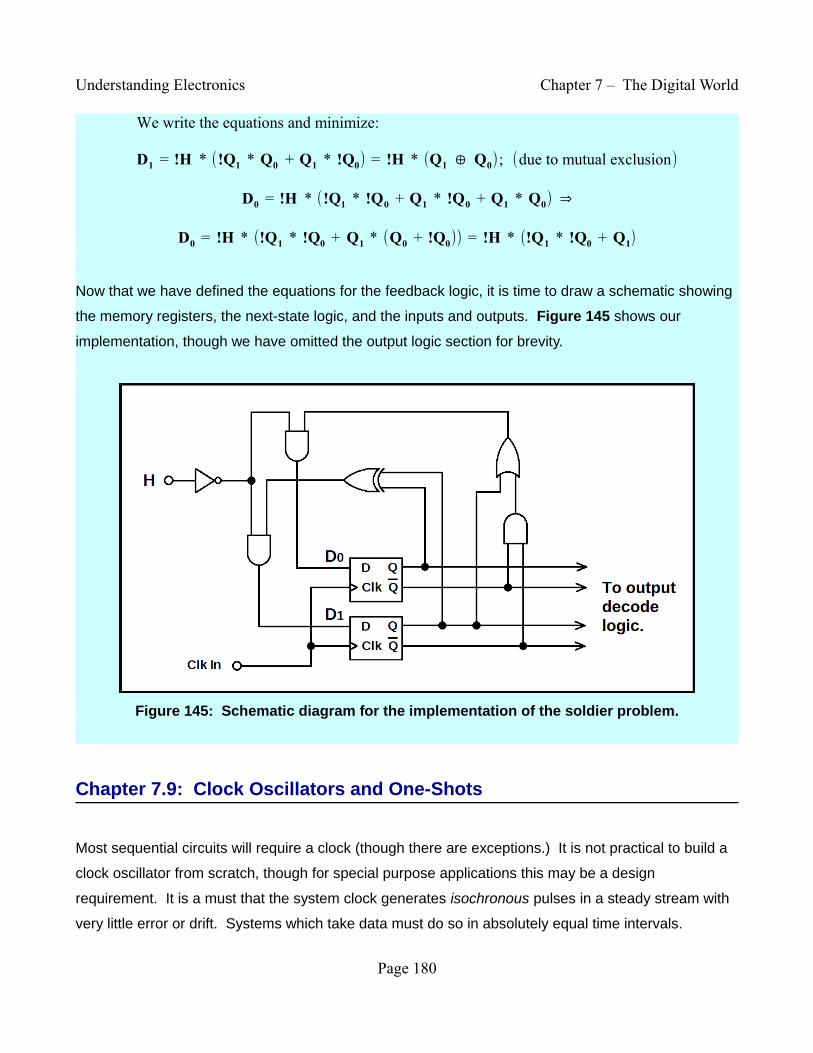
We write the equations and minimize:
D1 = !H * (!Q1 * Q0 + Q1 * !Q0) = !H * (Q1 ⊕ Q0); (due to mutual exclusion)
D0 = !H * (!Q1 * !Q0 + Q1 * !Q0 + Q1 * Q0) ⇒
D0 = !H * (!Q1 * !Q0 + Q1 * (Q0 + !Q0)) = !H * (!Q1 * !Q0 + Q1)
Now that we have defined the equations for the feedback logic, it is time to draw a schematic showing
the memory registers, the next-state logic, and the inputs and outputs. Figure 145 shows our
implementation, though we have omitted the output logic section for brevity.
Figure 145: Schematic diagram for the implementation of the soldier problem.
Chapter 7.9: Clock Oscillators and One-Shots
Most sequential circuits will require a clock (though there are exceptions.) It is not practical to build a
clock oscillator from scratch, though for special purpose applications this may be a design
requirement. It is a must that the system clock generates isochronous pulses in a steady stream with
very little error or drift. Systems which take data must do so in absolutely equal time intervals.
Page 180
Understanding Electronics Chapter 7 – The Digital World
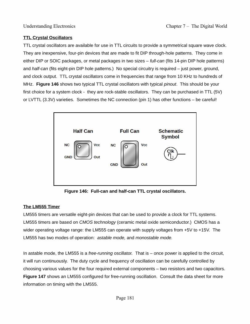
TTL Crystal Oscillators
TTL crystal oscillators are available for use in TTL circuits to provide a symmetrical square wave clock.
They are inexpensive, four-pin devices that are made to fit DIP through-hole patterns. They come in
either DIP or SOIC packages, or metal packages in two sizes – full-can (fits 14-pin DIP hole patterns)
and half-can (fits eight-pin DIP hole patterns.) No special circuitry is required – just power, ground,
and clock output. TTL crystal oscillators come in frequencies that range from 10 KHz to hundreds of
MHz. Figure 146 shows two typical TTL crystal oscillators with typical pinout. This should be your
first choice for a system clock - they are rock-stable oscillators. They can be purchased in TTL (5V)
or LVTTL (3.3V) varieties. Sometimes the NC connection (pin 1) has other functions – be careful!
Figure 146: Full-can and half-can TTL crystal oscillators.
The LM555 Timer
LM555 timers are versatile eight-pin devices that can be used to provide a clock for TTL systems.
LM555 timers are based on CMOS technology (ceramic metal oxide semiconductor.) CMOS has a
wider operating voltage range: the LM555 can operate with supply voltages from +5V to +15V. The
LM555 has two modes of operation: astable mode, and monostable mode.
In astable mode, the LM555 is a free-running oscillator. That is – once power is applied to the circuit,
it will run continuously. The duty cycle and frequency of oscillation can be carefully controlled by
choosing various values for the four required external components – two resistors and two capacitors.
Figure 147 shows an LM555 configured for free-running oscillation. Consult the data sheet for more
information on timing with the LM555.
Page 181

Understanding Electronics Chapter 7 – The Digital World
Figure 147: LM555 timer configured as a free-running oscillator.
Monostable mode differs from astable mode in that it does not run freely. The output will idle low until
the circuit is triggered. Then, the output goes high and ignores all other trigger events until the circuit
times and and the output goes low again. When the pulse times out, it is ready for another trigger.
Figure 148 shows a monostable pulse circuit with a pulse delay of 0.627 seconds.
Figure 148: LM555 one-shot (monostable) timer being used as a switch debounce.
Page 182
Understanding Electronics Chapter 7 – The Digital World
Monostable (one-shot) mode oscillator circuits have a wide variety of uses. They can be used to turn
on / off a piece of equipment or circuit for a specific amount of time. The on-time of the pulse can be
adjusted from fractions of a second to hours – making these ICs useful for auto-shutoff (“green
technology”) circuits. Alternatively, they can be used to debounce switches. (Switch bounce is caused
by mechanical vibrations as the switch mechanism closes.)
Chapter 7.10: Counters
Counters are digital devices that are composed of flip-flops that can increment or decrement a binary
value. They often feature an up / down control line to control the count direction, and also other
functions such as enable and clear. Counters are useful for keeping track of events that are too fast to
tally by hand. They are also useful for measuring time – a window counter can very accurately
measure time intervals. Let's have a look at how counters are constructed.
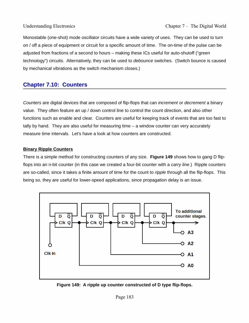
Binary Ripple Counters
There is a simple method for constructing counters of any size. Figure 149 shows how to gang D flip-
flops into an n-bit counter (in this case we created a four-bit counter with a carry line.) Ripple counters
are so-called, since it takes a finite amount of time for the count to ripple through all the flip-flops. This
being so, they are useful for lower-speed applications, since propagation delay is an issue.
Figure 149: A ripple up counter constructed of D type flip-flops.
Page 183
Understanding Electronics Chapter 7 – The Digital World
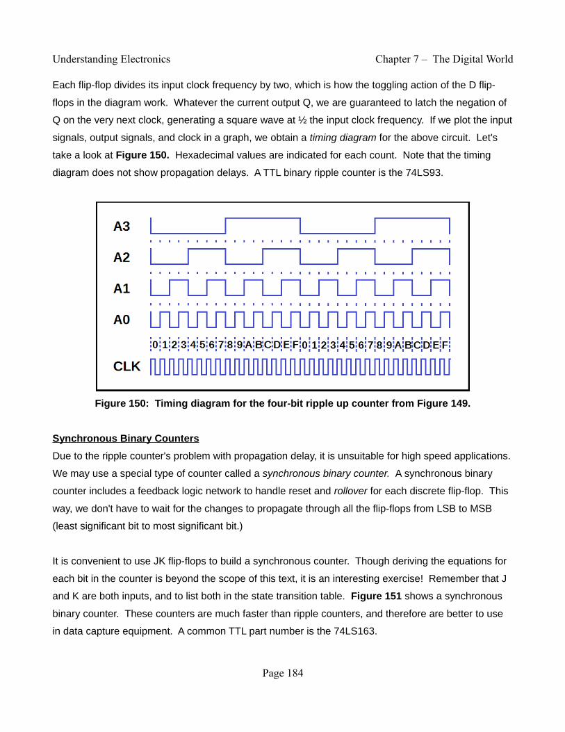
Each flip-flop divides its input clock frequency by two, which is how the toggling action of the D flip-
flops in the diagram work. Whatever the current output Q, we are guaranteed to latch the negation of
Q on the very next clock, generating a square wave at ½ the input clock frequency. If we plot the input
signals, output signals, and clock in a graph, we obtain a timing diagram for the above circuit. Let's
take a look at Figure 150. Hexadecimal values are indicated for each count. Note that the timing
diagram does not show propagation delays. A TTL binary ripple counter is the 74LS93.
Figure 150: Timing diagram for the four-bit ripple up counter from Figure 149.
Synchronous Binary Counters
Due to the ripple counter's problem with propagation delay, it is unsuitable for high speed applications.
We may use a special type of counter called a synchronous binary counter. A synchronous binary
counter includes a feedback logic network to handle reset and rollover for each discrete flip-flop. This
way, we don't have to wait for the changes to propagate through all the flip-flops from LSB to MSB
(least significant bit to most significant bit.)
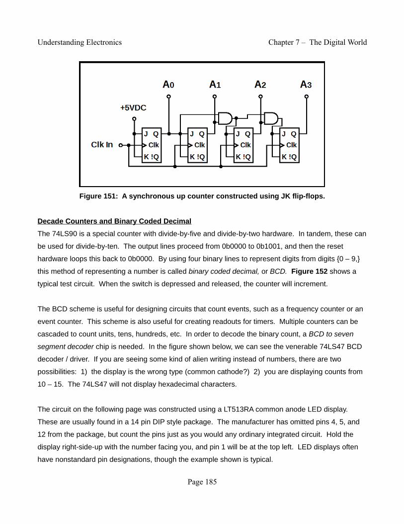
It is convenient to use JK flip-flops to build a synchronous counter. Though deriving the equations for
each bit in the counter is beyond the scope of this text, it is an interesting exercise! Remember that J
and K are both inputs, and to list both in the state transition table. Figure 151 shows a synchronous
binary counter. These counters are much faster than ripple counters, and therefore are better to use
in data capture equipment. A common TTL part number is the 74LS163.
Page 184
Understanding Electronics Chapter 7 – The Digital World
Figure 151: A synchronous up counter constructed using JK flip-flops.
Decade Counters and Binary Coded Decimal
The 74LS90 is a special counter with divide-by-five and divide-by-two hardware. In tandem, these can
be used for divide-by-ten. The output lines proceed from 0b0000 to 0b1001, and then the reset
hardware loops this back to 0b0000. By using four binary lines to represent digits from digits {0 – 9,}
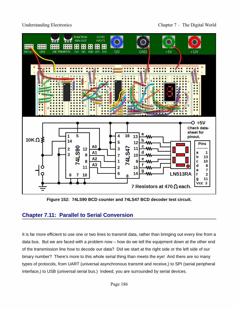
this method of representing a number is called binary coded decimal, or BCD. Figure 152 shows a
typical test circuit. When the switch is depressed and released, the counter will increment.
The BCD scheme is useful for designing circuits that count events, such as a frequency counter or an
event counter. This scheme is also useful for creating readouts for timers. Multiple counters can be
cascaded to count units, tens, hundreds, etc. In order to decode the binary count, a BCD to seven
segment decoder chip is needed. In the figure shown below, we can see the venerable 74LS47 BCD
decoder / driver. If you are seeing some kind of alien writing instead of numbers, there are two
possibilities: 1) the display is the wrong type (common cathode?) 2) you are displaying counts from
10 – 15. The 74LS47 will not display hexadecimal characters.
The circuit on the following page was constructed using a LT513RA common anode LED display.
These are usually found in a 14 pin DIP style package. The manufacturer has omitted pins 4, 5, and
12 from the package, but count the pins just as you would any ordinary integrated circuit. Hold the
display right-side-up with the number facing you, and pin 1 will be at the top left. LED displays often
have nonstandard pin designations, though the example shown is typical.
Page 185
Understanding Electronics Chapter 7 – The Digital World
Figure 152: 74LS90 BCD counter and 74LS47 BCD decoder test circuit.
Chapter 7.11: Parallel to Serial Conversion
It is far more efficient to use one or two lines to transmit data, rather than bringing out every line from a
data bus. But we are faced with a problem now – how do we tell the equipment down at the other end
of the transmission line how to decode our data? Did we start at the right side or the left side of our
binary number? There's more to this whole serial thing than meets the eye! And there are so many
types of protocols, from UART (universal asynchronous transmit and receive,) to SPI (serial peripheral
interface,) to USB (universal serial bus.) Indeed, you are surrounded by serial devices.
Page 186
Understanding Electronics Chapter 7 – The Digital World
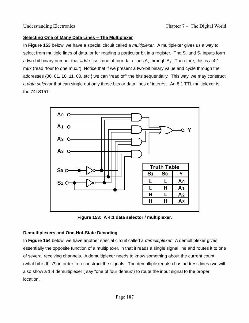
Selecting One of Many Data Lines – The Multiplexer
In Figure 153 below, we have a special circuit called a multiplexer. A multiplexer gives us a way to
select from multiple lines of data, or for reading a particular bit in a register. The S0 and S1 inputs form
a two-bit binary number that addresses one of four data lines A0 through A3. Therefore, this is a 4:1
mux (read “four to one mux.”) Notice that if we present a two-bit binary value and cycle through the
addresses {00, 01, 10, 11, 00, etc.} we can “read off” the bits sequentially. This way, we may construct
a data selector that can single out only those bits or data lines of interest. An 8:1 TTL multiplexer is
the 74LS151.
Figure 153: A 4:1 data selector / multiplexer.
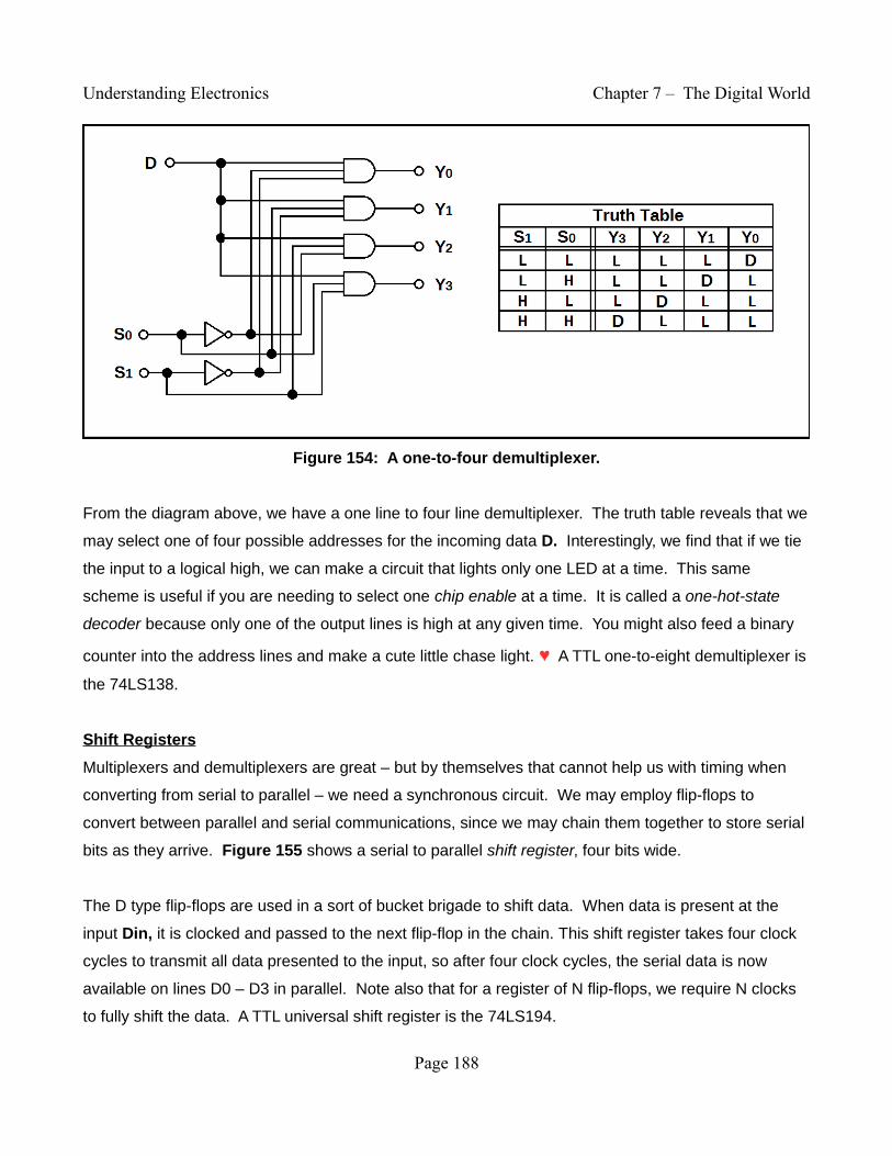
Demultiplexers and One-Hot-State Decoding
In Figure 154 below, we have another special circuit called a demultiplexer. A demultiplexer gives
essentially the opposite function of a multiplexer, in that it reads a single signal line and routes it to one
of several receiving channels. A demultiplexer needs to know something about the current count
(what bit is this?) in order to reconstruct the signals. The demultiplexer also has address lines (we will
also show a 1:4 demultiplexer ( say “one of four demux”) to route the input signal to the proper
location.
Page 187
Understanding Electronics Chapter 7 – The Digital World
Figure 154: A one-to-four demultiplexer.
From the diagram above, we have a one line to four line demultiplexer. The truth table reveals that we
may select one of four possible addresses for the incoming data D. Interestingly, we find that if we tie
the input to a logical high, we can make a circuit that lights only one LED at a time. This same
scheme is useful if you are needing to select one chip enable at a time. It is called a one-hot-state
decoder because only one of the output lines is high at any given time. You might also feed a binary
counter into the address lines and make a cute little chase light. ♥ A TTL one-to-eight demultiplexer is
the 74LS138.
Shift Registers
Multiplexers and demultiplexers are great – but by themselves that cannot help us with timing when
converting from serial to parallel – we need a synchronous circuit. We may employ flip-flops to
convert between parallel and serial communications, since we may chain them together to store serial
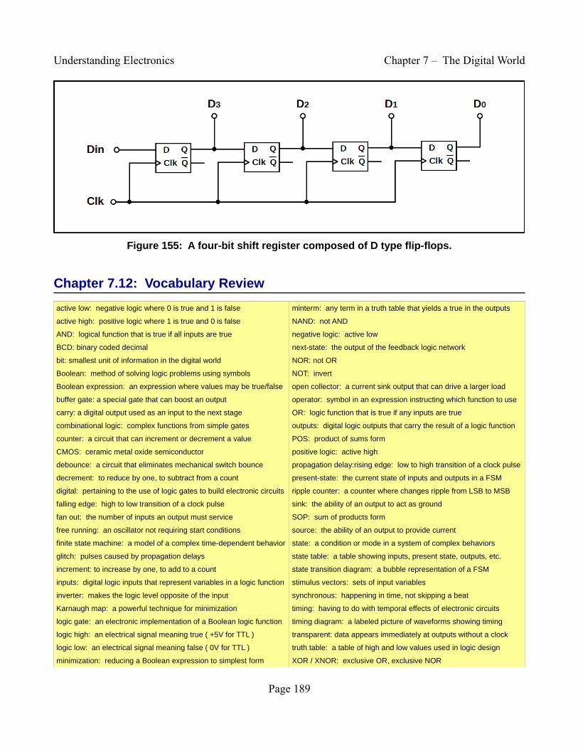
bits as they arrive. Figure 155 shows a serial to parallel shift register, four bits wide.
The D type flip-flops are used in a sort of bucket brigade to shift data. When data is present at the
input Din, it is clocked and passed to the next flip-flop in the chain. This shift register takes four clock
cycles to transmit all data presented to the input, so after four clock cycles, the serial data is now
available on lines D0 – D3 in parallel. Note also that for a register of N flip-flops, we require N clocks
to fully shift the data. A TTL universal shift register is the 74LS194.
Page 188
Understanding Electronics Chapter 7 – The Digital World
Figure 155: A four-bit shift register composed of D type flip-flops.
Chapter 7.12: Vocabulary Review
active low: negative logic where 0 is true and 1 is false
active high: positive logic where 1 is true and 0 is false
AND: logical function that is true if all inputs are true
BCD: binary coded decimal
bit: smallest unit of information in the digital world
Boolean: method of solving logic problems using symbols
Boolean expression: an expression where values may be true/false
buffer gate: a special gate that can boost an output
carry: a digital output used as an input to the next stage
combinational logic: complex functions from simple gates
counter: a circuit that can increment or decrement a value
CMOS: ceramic metal oxide semiconductor
debounce: a circuit that eliminates mechanical switch bounce
decrement: to reduce by one, to subtract from a count
digital: pertaining to the use of logic gates to build electronic circuits
falling edge: high to low transition of a clock pulse
fan out: the number of inputs an output must service
free running: an oscillator not requiring start conditions
finite state machine: a model of a complex time-dependent behavior
glitch: pulses caused by propagation delays
increment: to increase by one, to add to a count
inputs: digital logic inputs that represent variables in a logic function
inverter: makes the logic level opposite of the input
Karnaugh map: a powerful technique for minimization
logic gate: an electronic implementation of a Boolean logic function
logic high: an electrical signal meaning true ( +5V for TTL )
logic low: an electrical signal meaning false ( 0V for TTL )
minimization: reducing a Boolean expression to simplest form
minterm: any term in a truth table that yields a true in the outputs
NAND: not AND
negative logic: active low
next-state: the output of the feedback logic network
NOR: not OR
NOT: invert
open collector: a current sink output that can drive a larger load
operator: symbol in an expression instructing which function to use
OR: logic function that is true if any inputs are true
outputs: digital logic outputs that carry the result of a logic function
POS: product of sums form
positive logic: active high
propagation delay:rising edge: low to high transition of a clock pulse
present-state: the current state of inputs and outputs in a FSM
ripple counter: a counter where changes ripple from LSB to MSB
sink: the ability of an output to act as ground
SOP: sum of products form
source: the ability of an output to provide current
state: a condition or mode in a system of complex behaviors
state table: a table showing inputs, present state, outputs, etc.
state transition diagram: a bubble representation of a FSM
stimulus vectors: sets of input variables
synchronous: happening in time, not skipping a beat
timing: having to do with temporal effects of electronic circuits
timing diagram: a labeled picture of waveforms showing timing
transparent: data appears immediately at outputs without a clock
truth table: a table of high and low values used in logic design
XOR / XNOR: exclusive OR, exclusive NOR
Page 189
Understanding Electronics Chapter 7 – The Digital World
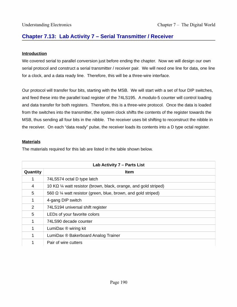
Chapter 7.13: Lab Activity 7 – Serial Transmitter / Receiver
Introduction
We covered serial to parallel conversion just before ending the chapter. Now we will design our own
serial protocol and construct a serial transmitter / receiver pair. We will need one line for data, one line
for a clock, and a data ready line. Therefore, this will be a three-wire interface.
Our protocol will transfer four bits, starting with the MSB. We will start with a set of four DIP switches,
and feed these into the parallel load register of the 74LS195. A modulo-5 counter will control loading
and data transfer for both registers. Therefore, this is a three-wire protocol. Once the data is loaded
from the switches into the transmitter, the system clock shifts the contents of the register towards the
MSB, thus sending all four bits in the nibble. The receiver uses bit shifting to reconstruct the nibble in
the receiver. On each “data ready” pulse, the receiver loads its contents into a D type octal register.
Materials
The materials required for this lab are listed in the table shown below.
Lab Activity 7 – Parts List
Quantity Item
1 74LS574 octal D type latch
4 10 KΩ ¼ watt resistor (brown, black, orange, and gold striped)
5 560 Ω ¼ watt resistor (green, blue, brown, and gold striped)
1 4-gang DIP switch
2 74LS194 universal shift register
5 LEDs of your favorite colors
1 74LS90 decade counter
1 LumiDax ® wiring kit
1 LumiDax ® Bakerboard Analog Trainer
1 Pair of wire cutters
Page 190
Understanding Electronics Chapter 7 – The Digital World
Procedure
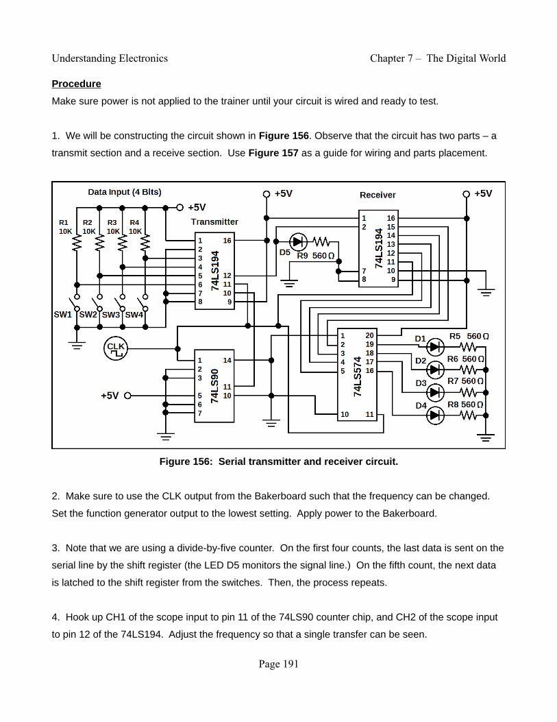
Make sure power is not applied to the trainer until your circuit is wired and ready to test.
1. We will be constructing the circuit shown in Figure 156. Observe that the circuit has two parts – a
transmit section and a receive section. Use Figure 157 as a guide for wiring and parts placement.
Figure 156: Serial transmitter and receiver circuit.
2. Make sure to use the CLK output from the Bakerboard such that the frequency can be changed.
Set the function generator output to the lowest setting. Apply power to the Bakerboard.
3. Note that we are using a divide-by-five counter. On the first four counts, the last data is sent on the
serial line by the shift register (the LED D5 monitors the signal line.) On the fifth count, the next data
is latched to the shift register from the switches. Then, the process repeats.
4. Hook up CH1 of the scope input to pin 11 of the 74LS90 counter chip, and CH2 of the scope input
to pin 12 of the 74LS194. Adjust the frequency so that a single transfer can be seen.
Page 191
Understanding Electronics Chapter 7 – The Digital World
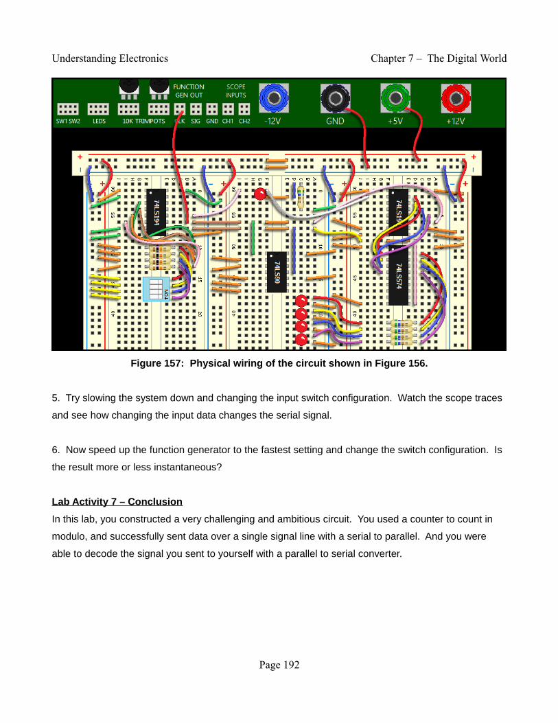
Figure 157: Physical wiring of the circuit shown in Figure 156.
5. Try slowing the system down and changing the input switch configuration. Watch the scope traces
and see how changing the input data changes the serial signal.
6. Now speed up the function generator to the fastest setting and change the switch configuration. Is
the result more or less instantaneous?
Lab Activity 7 – Conclusion
In this lab, you constructed a very challenging and ambitious circuit. You used a counter to count in
modulo, and successfully sent data over a single signal line with a serial to parallel. And you were
able to decode the signal you sent to yourself with a parallel to serial converter.
Page 192
Understanding Electronics Chapter 7 – The Digital World
Chapter 7.14: Exercises
Vocabulary Questions
1. If we use 0 as logic high and 1 as logic low, this is _________________ logic.
2. When designing digital logic, minimization is helped with _______________________ maps.
3. A ______________________ uses flip-flops to increment or decrement a value.
4. When we put many signals on one line, this is called ________________.
5. A __________________ decoder allows only one state to be logic high at a time.
6. A ___________________ is a collection of latches or flip-flops for storing data.
7. ___________________ is a branch of mathematics concerned with true or false values.
8. ___________________ logic uses simple gate logic to construct complex circuits.
9. _______________________ logic is time-dependent and involves one or more states.
10. _______________________ are used to map out complex behavior in a sequential circuit.
11. The __________________ outputs a logic high only when both inputs are high.
12. The __________________ negates the value appearing on its input.
13. An ____________________ outputs high if one and only one of its two inputs is high.
True or False
1. Both positive and negative logic are used in electronics. T F
2. A logic high is +5V. T F
3. A logic low is 0V. T F
4. A shift register is used for changing from positive to negative logic. T F
5. 10 could be 16, ten, or two, depending on the number system. ;-) T F
6. We may cascade AND and OR gates to get more inputs. (Think!) T F
7. Minimizing is an unnecessary step. (Careful...) T F
8. We may connect two outputs together without incident. T F
Page 193
Understanding Electronics Chapter 7 – The Digital World
Problems
1. Design an XOR gate using only AND, OR, and INVERT.
2. Design a feedback network that can detect the binary number 14 on a four bit register.
3. Design a simple shift register using six D-type flip-flops.
4. Convert the following binary number to decimal and hexadecimal: 0b01101001.
5. Simplify the following Boolean expression: A(!B * C + B * !C) + !A(!B * C + B * !C)
6. Draw a state transition diagram for your daily routine. Indicate any arrows or conditions.
7. In your own words, describe the process of converting from serial to parallel.
Page 194
This PDF is an excerpt from: Understanding Electronics – A Beginner's Guide with Projects, by Jonathan Baumgardner. Copyright © 2014 by LumiDax Electronics LLC. All rights reserved. No part of this book may be duplicated without permission from LumiDax Electronics LLC or the author. Educational use is permitted.

![CDM [2ex]Boolean Decision Diagrams [3ex]sutner/CDM/pdf/lect-27.pdf · Boolean Functions as Languages 16 Suppose we have some Boolean function f: 2n!2. In the spirit of disjunctive](https://static.fdocuments.us/doc/165x107/5fc4510ebd765034da4b13dd/cdm-2exboolean-decision-diagrams-3ex-sutnercdmpdflect-27pdf-boolean-functions.jpg)